WO2019221012A1 - 感光性フィルム及び永久マスクレジストの形成方法 - Google Patents
感光性フィルム及び永久マスクレジストの形成方法 Download PDFInfo
- Publication number
- WO2019221012A1 WO2019221012A1 PCT/JP2019/018615 JP2019018615W WO2019221012A1 WO 2019221012 A1 WO2019221012 A1 WO 2019221012A1 JP 2019018615 W JP2019018615 W JP 2019018615W WO 2019221012 A1 WO2019221012 A1 WO 2019221012A1
- Authority
- WO
- WIPO (PCT)
- Prior art keywords
- photosensitive
- film
- carrier film
- layer
- photosensitive layer
- Prior art date
- Legal status (The legal status is an assumption and is not a legal conclusion. Google has not performed a legal analysis and makes no representation as to the accuracy of the status listed.)
- Ceased
Links
Images

Classifications
-
- G—PHYSICS
- G03—PHOTOGRAPHY; CINEMATOGRAPHY; ANALOGOUS TECHNIQUES USING WAVES OTHER THAN OPTICAL WAVES; ELECTROGRAPHY; HOLOGRAPHY
- G03F—PHOTOMECHANICAL PRODUCTION OF TEXTURED OR PATTERNED SURFACES, e.g. FOR PRINTING, FOR PROCESSING OF SEMICONDUCTOR DEVICES; MATERIALS THEREFOR; ORIGINALS THEREFOR; APPARATUS SPECIALLY ADAPTED THEREFOR
- G03F7/00—Photomechanical, e.g. photolithographic, production of textured or patterned surfaces, e.g. printing surfaces; Materials therefor, e.g. comprising photoresists; Apparatus specially adapted therefor
- G03F7/004—Photosensitive materials
- G03F7/09—Photosensitive materials characterised by structural details, e.g. supports, auxiliary layers
- G03F7/092—Photosensitive materials characterised by structural details, e.g. supports, auxiliary layers characterised by backside coating or layers, by lubricating-slip layers or means, by oxygen barrier layers or by stripping-release layers or means
-
- G—PHYSICS
- G03—PHOTOGRAPHY; CINEMATOGRAPHY; ANALOGOUS TECHNIQUES USING WAVES OTHER THAN OPTICAL WAVES; ELECTROGRAPHY; HOLOGRAPHY
- G03F—PHOTOMECHANICAL PRODUCTION OF TEXTURED OR PATTERNED SURFACES, e.g. FOR PRINTING, FOR PROCESSING OF SEMICONDUCTOR DEVICES; MATERIALS THEREFOR; ORIGINALS THEREFOR; APPARATUS SPECIALLY ADAPTED THEREFOR
- G03F7/00—Photomechanical, e.g. photolithographic, production of textured or patterned surfaces, e.g. printing surfaces; Materials therefor, e.g. comprising photoresists; Apparatus specially adapted therefor
- G03F7/004—Photosensitive materials
- G03F7/0047—Photosensitive materials characterised by additives for obtaining a metallic or ceramic pattern, e.g. by firing
-
- G—PHYSICS
- G03—PHOTOGRAPHY; CINEMATOGRAPHY; ANALOGOUS TECHNIQUES USING WAVES OTHER THAN OPTICAL WAVES; ELECTROGRAPHY; HOLOGRAPHY
- G03F—PHOTOMECHANICAL PRODUCTION OF TEXTURED OR PATTERNED SURFACES, e.g. FOR PRINTING, FOR PROCESSING OF SEMICONDUCTOR DEVICES; MATERIALS THEREFOR; ORIGINALS THEREFOR; APPARATUS SPECIALLY ADAPTED THEREFOR
- G03F7/00—Photomechanical, e.g. photolithographic, production of textured or patterned surfaces, e.g. printing surfaces; Materials therefor, e.g. comprising photoresists; Apparatus specially adapted therefor
- G03F7/004—Photosensitive materials
-
- G—PHYSICS
- G03—PHOTOGRAPHY; CINEMATOGRAPHY; ANALOGOUS TECHNIQUES USING WAVES OTHER THAN OPTICAL WAVES; ELECTROGRAPHY; HOLOGRAPHY
- G03F—PHOTOMECHANICAL PRODUCTION OF TEXTURED OR PATTERNED SURFACES, e.g. FOR PRINTING, FOR PROCESSING OF SEMICONDUCTOR DEVICES; MATERIALS THEREFOR; ORIGINALS THEREFOR; APPARATUS SPECIALLY ADAPTED THEREFOR
- G03F7/00—Photomechanical, e.g. photolithographic, production of textured or patterned surfaces, e.g. printing surfaces; Materials therefor, e.g. comprising photoresists; Apparatus specially adapted therefor
- G03F7/004—Photosensitive materials
- G03F7/09—Photosensitive materials characterised by structural details, e.g. supports, auxiliary layers
-
- G—PHYSICS
- G03—PHOTOGRAPHY; CINEMATOGRAPHY; ANALOGOUS TECHNIQUES USING WAVES OTHER THAN OPTICAL WAVES; ELECTROGRAPHY; HOLOGRAPHY
- G03F—PHOTOMECHANICAL PRODUCTION OF TEXTURED OR PATTERNED SURFACES, e.g. FOR PRINTING, FOR PROCESSING OF SEMICONDUCTOR DEVICES; MATERIALS THEREFOR; ORIGINALS THEREFOR; APPARATUS SPECIALLY ADAPTED THEREFOR
- G03F7/00—Photomechanical, e.g. photolithographic, production of textured or patterned surfaces, e.g. printing surfaces; Materials therefor, e.g. comprising photoresists; Apparatus specially adapted therefor
- G03F7/26—Processing photosensitive materials; Apparatus therefor
- G03F7/30—Imagewise removal using liquid means
-
- H—ELECTRICITY
- H05—ELECTRIC TECHNIQUES NOT OTHERWISE PROVIDED FOR
- H05K—PRINTED CIRCUITS; CASINGS OR CONSTRUCTIONAL DETAILS OF ELECTRIC APPARATUS; MANUFACTURE OF ASSEMBLAGES OF ELECTRICAL COMPONENTS
- H05K3/00—Apparatus or processes for manufacturing printed circuits
- H05K3/0073—Masks not provided for in groups H05K3/02 - H05K3/46, e.g. for photomechanical production of patterned surfaces
- H05K3/0076—Masks not provided for in groups H05K3/02 - H05K3/46, e.g. for photomechanical production of patterned surfaces characterised by the composition of the mask
-
- H—ELECTRICITY
- H05—ELECTRIC TECHNIQUES NOT OTHERWISE PROVIDED FOR
- H05K—PRINTED CIRCUITS; CASINGS OR CONSTRUCTIONAL DETAILS OF ELECTRIC APPARATUS; MANUFACTURE OF ASSEMBLAGES OF ELECTRICAL COMPONENTS
- H05K3/00—Apparatus or processes for manufacturing printed circuits
- H05K3/0073—Masks not provided for in groups H05K3/02 - H05K3/46, e.g. for photomechanical production of patterned surfaces
- H05K3/0079—Masks not provided for in groups H05K3/02 - H05K3/46, e.g. for photomechanical production of patterned surfaces characterised by the method of application or removal of the mask
-
- H—ELECTRICITY
- H05—ELECTRIC TECHNIQUES NOT OTHERWISE PROVIDED FOR
- H05K—PRINTED CIRCUITS; CASINGS OR CONSTRUCTIONAL DETAILS OF ELECTRIC APPARATUS; MANUFACTURE OF ASSEMBLAGES OF ELECTRICAL COMPONENTS
- H05K3/00—Apparatus or processes for manufacturing printed circuits
- H05K3/22—Secondary treatment of printed circuits
- H05K3/28—Applying non-metallic protective coatings
- H05K3/281—Applying non-metallic protective coatings by means of a preformed insulating foil
-
- H—ELECTRICITY
- H05—ELECTRIC TECHNIQUES NOT OTHERWISE PROVIDED FOR
- H05K—PRINTED CIRCUITS; CASINGS OR CONSTRUCTIONAL DETAILS OF ELECTRIC APPARATUS; MANUFACTURE OF ASSEMBLAGES OF ELECTRICAL COMPONENTS
- H05K3/00—Apparatus or processes for manufacturing printed circuits
- H05K3/30—Assembling printed circuits with electric components, e.g. with resistors
- H05K3/32—Assembling printed circuits with electric components, e.g. with resistors electrically connecting electric components or wires to printed circuits
- H05K3/34—Assembling printed circuits with electric components, e.g. with resistors electrically connecting electric components or wires to printed circuits by soldering
- H05K3/3452—Solder masks
-
- G—PHYSICS
- G03—PHOTOGRAPHY; CINEMATOGRAPHY; ANALOGOUS TECHNIQUES USING WAVES OTHER THAN OPTICAL WAVES; ELECTROGRAPHY; HOLOGRAPHY
- G03F—PHOTOMECHANICAL PRODUCTION OF TEXTURED OR PATTERNED SURFACES, e.g. FOR PRINTING, FOR PROCESSING OF SEMICONDUCTOR DEVICES; MATERIALS THEREFOR; ORIGINALS THEREFOR; APPARATUS SPECIALLY ADAPTED THEREFOR
- G03F7/00—Photomechanical, e.g. photolithographic, production of textured or patterned surfaces, e.g. printing surfaces; Materials therefor, e.g. comprising photoresists; Apparatus specially adapted therefor
- G03F7/004—Photosensitive materials
- G03F7/027—Non-macromolecular photopolymerisable compounds having carbon-to-carbon double bonds, e.g. ethylenic compounds
-
- G—PHYSICS
- G03—PHOTOGRAPHY; CINEMATOGRAPHY; ANALOGOUS TECHNIQUES USING WAVES OTHER THAN OPTICAL WAVES; ELECTROGRAPHY; HOLOGRAPHY
- G03F—PHOTOMECHANICAL PRODUCTION OF TEXTURED OR PATTERNED SURFACES, e.g. FOR PRINTING, FOR PROCESSING OF SEMICONDUCTOR DEVICES; MATERIALS THEREFOR; ORIGINALS THEREFOR; APPARATUS SPECIALLY ADAPTED THEREFOR
- G03F7/00—Photomechanical, e.g. photolithographic, production of textured or patterned surfaces, e.g. printing surfaces; Materials therefor, e.g. comprising photoresists; Apparatus specially adapted therefor
- G03F7/004—Photosensitive materials
- G03F7/038—Macromolecular compounds which are rendered insoluble or differentially wettable
-
- H—ELECTRICITY
- H05—ELECTRIC TECHNIQUES NOT OTHERWISE PROVIDED FOR
- H05K—PRINTED CIRCUITS; CASINGS OR CONSTRUCTIONAL DETAILS OF ELECTRIC APPARATUS; MANUFACTURE OF ASSEMBLAGES OF ELECTRICAL COMPONENTS
- H05K2203/00—Indexing scheme relating to apparatus or processes for manufacturing printed circuits covered by H05K3/00
- H05K2203/01—Tools for processing; Objects used during processing
- H05K2203/0147—Carriers and holders
- H05K2203/0156—Temporary polymeric carrier or foil, e.g. for processing or transferring
Definitions
- the present invention relates to a method for forming a photosensitive film and a permanent mask resist.
- a photosensitive film in which a layer formed from a photosensitive resin composition (hereinafter referred to as “photosensitive layer”) is formed on a support film (carrier film) is widely used.
- photosensitive layer a layer formed from a photosensitive resin composition
- carrier film carrier film
- the permanent mask resist needs to have excellent adhesion to the laminated material.
- the surface of the resist pattern is roughened by plasma treatment or the like. Therefore, the process of forming a permanent mask resist using a photosensitive film is complicated. Therefore, it is required not only to form a resist pattern having excellent resolution, but also to form a permanent mask resist having excellent adhesion by omitting the step of roughening the surface of the resist pattern.
- An object of the present invention is to provide a photosensitive film capable of easily forming a resist pattern excellent in resolution and adhesion, and a method for forming a permanent mask resist using the photosensitive film.
- One aspect of the present invention is a photosensitive film comprising a carrier film having a first surface with a surface roughness of 0.1 to 0.4 ⁇ m, and a photosensitive layer formed on the first surface.
- the carrier film has a haze of 30 to 65%, and a transparent resin layer having a refractive index within ⁇ 0.02 of the refractive index of the photosensitive layer is provided on the first surface.
- the present invention relates to a photosensitive film having a spectral haze at a wavelength of 405 nm of 0.1 to 9.0%.
- the carrier film may have a resin layer containing inorganic particles and a binder resin on the first surface side.
- the resin layer may contain inorganic particles having an average particle size of 0.1 to 3.0 ⁇ m.
- Another aspect of the present invention comprises a step of laminating the photosensitive film on a substrate in the order of a photosensitive layer and a carrier film, and irradiating a predetermined portion of the photosensitive layer with an actinic ray through the carrier film to form a photosensitive layer. And forming a resist pattern by removing portions other than the photocured portion after the carrier film is peeled off, and the surface roughness of the resist pattern is 0.1-0.
- the present invention relates to a method for forming a permanent mask resist having a thickness of 4 ⁇ m.
- the present invention it is possible to provide a photosensitive film capable of easily forming a resist pattern excellent in resolution and adhesion, and a method for forming a permanent mask resist using the photosensitive film.
- the term “layer” includes a structure formed in a part in addition to a structure formed over the entire surface when observed as a plan view.
- the numerical range indicated by using “to” indicates a range including the numerical values described before and after “to” as the minimum value and the maximum value, respectively.
- the upper limit value or lower limit value of a numerical range of a certain step may be replaced with the upper limit value or lower limit value of the numerical range of another step.
- the upper limit value or the lower limit value of the numerical range may be replaced with the values shown in the examples.
- the photosensitive film of the present embodiment includes a carrier film having a first surface with a surface roughness of 0.1 to 0.4 ⁇ m, and a photosensitive layer formed on the first surface.
- a transparent resin layer having a refractive index within a range of ⁇ 0.02 with respect to the refractive index of the photosensitive layer having a haze of 30 to 65% and measured on the first surface is 405 nm.
- Spectral haze at a wavelength is 0.1 to 9.0%.
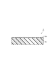
- FIG. 1 is a schematic cross-sectional view for explaining an example of a carrier film according to this embodiment.
- the carrier film 1 can have the base material layer 1b and the resin layer 1a formed in one surface of the base material layer 1b. Concavities and convexities are formed on the surface of the resin layer 1a serving as the first surface.
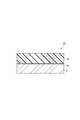
- FIG. 2 is a schematic cross-sectional view for explaining an example of the photosensitive film according to the present embodiment.
- a photosensitive film 10 shown in FIG. 2 includes a carrier film 1 including a base layer 1 b and a resin layer 1 a, and a photosensitive layer 2 provided on the resin layer 1 a of the carrier film 1.
- a polymer film having optical transparency can be used as the base material layer 1b.
- the total light transmittance of the base material layer 1b is preferably 85% or more, and more preferably 90% or more.
- the haze of the base material layer 1b is preferably 4% or less, more preferably 2% or less, and still more preferably 1% or less.
- Examples of such a polymer film include a polyester film such as a polyethylene terephthalate film, and a polyolefin film such as a polyethylene film and a polypropylene film.
- the thickness of the base material layer 1b is, for example, 5 to 250 ⁇ m.
- the thickness of the base material layer 1b is preferably from 5 to 100 ⁇ m, more preferably from 10 to 70 ⁇ m, still more preferably from 15 to 40 ⁇ m, from the viewpoints of handleability and resolution. Particularly preferred is 35 ⁇ m.
- the thickness of the base material layer 1b is 5 ⁇ m or more, the handleability is excellent, and when the thickness is 250 ⁇ m or less, the distance from the photomask to the photosensitive layer can be adjusted, and the degradation of resolution due to the influence of the diffraction phenomenon is suppressed. It becomes easy.
- the resin layer 1a can contain inorganic particles and a binder resin. From the viewpoint of adjusting the surface roughness to the target range, the inorganic particles are preferably contained in the resin layer 1a in an amount of 1 to 20% by mass, and more preferably 1 to 10% by mass.
- the resin layer 1a contains inorganic particles, it becomes easy to form irregularities having a surface roughness of 0.1 to 0.4 ⁇ m on the surface (first surface) in contact with the photosensitive layer of the carrier film. And it becomes easy to transfer the shape of the unevenness onto the surface of the photosensitive layer.
- the inorganic particles include silica particles, calcium carbonate particles, alumina particles, titanium oxide particles, and barium sulfate particles. From the viewpoint of reducing the refractive index difference between the inorganic particles and the binder resin, silica particles are preferably used as the inorganic particles.
- the resin layer 1a may include inorganic particles having an average particle diameter of 0.1 to 3.0 ⁇ m. Since the surface roughness can be easily adjusted, the average particle diameter of the inorganic particles contained in the resin layer 1a may be 0.5 to 3.0 ⁇ m or 1.0 to 2.8 ⁇ m.
- thermosetting resin for example, an acrylic resin, a urethane resin, or the like.
- the difference in the refractive index of the binder resin from the refractive index of the photosensitive layer 2 provided in optical contact with the resin layer 1a is better from the viewpoint of resolution.
- the absolute value of the difference in refractive index between the resin layer 1a and the photosensitive layer 2 is preferably 0.2 or less, more preferably 0.1 or less, still more preferably 0.05 or less, and 0.02 or less. Is particularly preferred.
- the thickness of the resin layer 1a may be, for example, 0.5 to 8 ⁇ m, 1 to 5 ⁇ m, or 2.5 to 4.5 ⁇ m.
- the thickness of the resin layer 1a is obtained by subtracting the thickness of the base material layer 1b from the total thickness of the carrier film according to JIS K5600-1-7: 2014.
- the total thickness of the carrier film can be measured by using a micrometer having a flat measurement surface or a dial gauge having a flat measuring element, and the resin layer 1a of the base material layer 1b is not formed. It is obtained as the distance between the surface and the convex top of the resin layer 1a having irregularities.
- the method for producing the carrier film according to this embodiment is not particularly limited.
- the carrier film may be produced, for example, by applying a coating liquid containing inorganic particles and a binder resin to the polymer film to be the base material layer 1b and then drying it while heating.
- a coating method for example, known methods such as roll coating, comma coating, gravure coating, air knife coating, die coating, and bar coating can be employed. Drying conditions may be, for example, 80 to 140 ° C. and 0.5 to 10 minutes.
- the surface roughness of the resin layer 1a serving as the first surface of the carrier film is 0.1 to 0.4 ⁇ m, preferably 0.1 to 0.35 ⁇ m, and preferably 0.1 to 0.3 ⁇ m. It is more preferable. If the surface roughness of the resin layer 1a exceeds 0.4 ⁇ m, the resolution of the resist pattern tends to decrease. When the surface roughness of the resin layer 1a is less than 0.1 ⁇ m, the adhesion of the formed permanent mask resist to the underfill or the like tends to be lowered. It is preferable that the 2nd surface which is a surface which is not in contact with the photosensitive layer of a carrier film is smooth. The surface roughness of the second surface is, for example, less than 0.1 ⁇ m. The second surface is the surface of the base material layer 1b on the side where the resin layer 1a is not formed.
- the surface roughness in this specification refers to the arithmetic average roughness (Ra) measured according to JIS B0601: 2013.
- the haze of the carrier film is 30 to 65%, but may be 31 to 64% or 33 to 63%. If the haze of the carrier film exceeds 65%, the resolution of the resist pattern tends to decrease. Further, if the haze of the carrier film is less than 30%, the adhesion of the formed permanent mask resist to the underfill or the like tends to be lowered. Haze can be measured according to JIS K7136: 2000.
- the total light transmittance (Tt) of the carrier film is preferably 80% or more, and more preferably 85% or more, from the viewpoint of energy efficiency during exposure.
- the total light transmittance can be measured according to JIS K7361-1: 1997.
- the photosensitive layer 2 is exposed to actinic rays transmitted through the carrier film 1.
- actinic rays In general, ultraviolet rays using a high-pressure mercury lamp, an ultrahigh-pressure mercury lamp, or the like as a light source are used as actinic rays. These ultraviolet rays are light rays having strong peaks at 365 nm (i-line), 405 nm (h-line), and 436 nm (g-line), which are mercury emission lines, due to the characteristics of the light source.
- the photosensitive layer contains a photopolymerization initiator having sensitivity to light of these wavelengths. For this reason, the scattering property with respect to light of these wavelengths has a great influence on the resolution of the photosensitive layer.
- the haze measured according to JIS K7136 is a measured value in the visible light region (380 to 780 nm), so it cannot be said that the behavior with respect to light of a specific wavelength used for exposure is described. Therefore, the present inventors have determined the spectral haze by measuring the light scattering property (haze) for each wavelength, and have studied in detail the influence of the spectral haze at the wavelength used for exposure on the resolution.
- Spectral haze at each wavelength is based on a transmission spectrum (measurement region: 350 to 800 nm) measured using a spectrophotometer (trade name “Solid Spec 3700” manufactured by Shimadzu Corporation), following JIS K7136. It can obtain
- Haze [( ⁇ 4 / ⁇ 2 ) ⁇ ( ⁇ 3 / ⁇ 1 )] ⁇ 100 (1)
- ⁇ 1 is a light beam incident on the integrating sphere without the sample
- ⁇ 2 is a light beam transmitted through the sample and incident on the integrating sphere
- ⁇ 3 is for removing parallel light without the sample.
- ⁇ 4 indicates the diffused light observed in the integrating sphere in which the trap for removing the parallel light through the sample is installed.
- the unevenness of the resin layer 1a of the carrier film 1 has light scattering (haze) as compared with the case of the carrier film 1 alone because the photosensitive layer 2 is in optical contact. to differ greatly. Therefore, in order to discuss the resolution of the photosensitive layer 2 in the photosensitive film 10, the haze (spectral haze) in the state of the photosensitive film 10 can be used.
- the photosensitive layer 2 may contain components (for example, inorganic fillers, pigments, etc.) that affect optical properties such as light scattering and light transmission in order to improve various properties. It may be difficult to directly measure 10 spectral hazes. Therefore, in this specification, spectral haze is conveniently evaluated using a laminated film in which a transparent resin layer made of a resin material not containing a component that affects optical properties is formed on the first surface of the carrier film. doing.
- a transparent resin having a refractive index within ⁇ 0.02 of the difference from the refractive index of the photosensitive resin composition forming the photosensitive layer 2 can be used.
- the refractive index in this specification can be measured using an Abbe refractometer according to JIS K7142: 2014.
- the spectral haze of the photosensitive film can be evaluated.
- the transparent resin can be appropriately selected according to the refractive index of the photosensitive resin composition forming the photosensitive layer 2.
- the thickness of the transparent resin layer is set according to the thickness of the photosensitive layer 2.
- the total light transmittance of the transparent resin layer according to the present embodiment is preferably 90% or more.
- the spectral haze at a wavelength of 405 nm of the laminated film provided with the transparent resin layer on the first surface of the carrier film is 0.1 to 9.0%, 0.1 to It is preferably 8.5%, more preferably 0.1 to 8.0%.
- the spectral haze of the laminated film at a wavelength of 365 nm may be 0.1 to 9.9%, 0.1 to 9.5%, or 0.1 to 9.1%.
- the spectral haze of the laminated film at a wavelength of 436 nm may be 0.1 to 8.5%, 0.1 to 7.5%, or 0.1 to 6.5%.
- the photosensitive layer 2 is a layer formed of a photosensitive resin composition.
- the photosensitive resin composition is not particularly limited as long as it is a material that can be used as a solder resist.
- the photosensitive resin composition may contain, for example, an acid-modified epoxy resin, a photopolymerizable compound, a photopolymerization initiator, an epoxy resin, and an inorganic filler.
- an acid-modified epoxy resin e.g., a photopolymerizable compound, a photopolymerization initiator, an epoxy resin, and an inorganic filler.
- the composition of the photosensitive resin composition is not limited to these components.
- the acid-modified epoxy resin may be, for example, a compound obtained by adding a polybasic acid anhydride to an esterified product of an epoxy resin and an ethylenically unsaturated group-containing monocarboxylic acid.
- the acid-modified epoxy resin include phenol novolac-type acid-modified epoxy acrylate, bisphenol F-type acid-modified epoxy acrylate, and urethane-modified bisphenol A-type acid-modified epoxy acrylate.
- the photopolymerizable compound is not particularly limited as long as it is a compound having a photopolymerizable functional group.
- the photopolymerizable functional group include ethylenically unsaturated groups such as vinyl group, allyl group, propargyl group, butenyl group, ethynyl group, phenylethynyl group, maleimide group, nadiimide group, and (meth) acryloyl group.
- the photopolymerizable compound preferably includes a compound having a (meth) acryloyl group.
- Examples of the photopolymerizable compound having one (meth) acryloyl group include hydroxyalkyl (meth) acrylates such as 2-hydroxyethyl (meth) acrylate and 2-hydroxypropyl (meth) acrylate.
- Examples of the photopolymerizable compound having two (meth) acryloyl groups include bisphenol A (meth) acrylate compounds, dimethylol tricyclodecane di (meth) acrylate, tricyclodecanediol di (meth) acrylate, and glycidyl groups. Examples thereof include compounds obtained by reacting the containing compound with an ⁇ , ⁇ -unsaturated carboxylic acid, and urethane di (meth) acrylate compounds.
- Examples of the photopolymerizable compound having three or more (meth) acryloyl groups include trimethylolpropane tri (meth) acrylate, tetramethylolmethanetri (meth) acrylate, tetramethylolmethanetetra (meth) acrylate, dipentaerythritol pentane.
- the photopolymerization initiator is not particularly limited as long as it matches the light wavelength of the exposure machine to be used, and a known one can be used.
- Examples of the photopolymerization initiator include alkylphenone photopolymerization initiators, acylphosphine oxide photopolymerization initiators, compounds having a thioxanthone skeleton, and titanocene photopolymerization initiators.
- epoxy resin examples include bisphenol A type epoxy resins such as bisphenol A diglycidyl ether, bisphenol F type epoxy resins such as bisphenol F diglycidyl ether, bisphenol S type epoxy resins such as bisphenol S diglycidyl ether, and biphenol diglycidyl ether.
- Biphenol type epoxy resin such as bixylenol diglycidyl ether, hydrogenated bisphenol A type epoxy resin such as hydrogenated bisphenol A glycidyl ether, phenol biphenyl aralkyl type epoxy resin and bisphenol novolac type epoxy resin It is done.
- inorganic fillers examples include silica, zirconia, barium sulfate, barium titanate, talc, clay, calcined kaolin, magnesium carbonate, calcium carbonate, calcium sulfate, zinc oxide, magnesium titanate, aluminum oxide, aluminum hydroxide, and mica powder. Is mentioned.
- the photosensitive resin composition may further contain a curing accelerator (curing catalyst).
- a curing accelerator curing accelerator
- the curing accelerator include imidazole, 2-methylimidazole, 2-ethylimidazole, 2-ethyl-4-methylimidazole, 2-phenylimidazole, 4-phenylimidazole, 1-cyanoethyl-2-phenylimidazole, 1- Imidazole compounds such as (2-cyanoethyl) -2-ethyl-4-methylimidazole; dicyandiamide, benzyldimethylamine, 4- (dimethylamino) -N, N-dimethylbenzylamine, 4-methoxy-N, N-dimethylbenzyl Examples thereof include amine compounds such as amine and 4-methyl-N, N-dimethylbenzylamine; and hydrazine compounds such as adipic hydrazide and sebacic acid hydrazide.
- the photosensitive resin composition may further contain a pigment.
- a pigment a colorant that develops a desired color when the wiring is concealed can be used.
- the pigment include known colorants or dyes such as phthalocyanine blue, phthalocyanine green, iodin green, malachite green, diazo yellow, crystal violet, titanium oxide, carbon black, and naphthalene black.
- a solvent may be used to mix the above-described components.
- the solvent include alcohol, glycol ether, ethylene glycol alkyl ether acetate, ketone, ester, and diethylene glycol.
- a curing accelerator In addition to the photosensitive resin composition, if necessary, a curing accelerator, an ultraviolet absorber, a silane coupling agent, a leveling agent, a plasticizer, an antifoaming agent, a flame retardant, an antioxidant, a polymerization inhibitor, etc. It may be added.
- the photosensitive layer 2 can be formed by applying a photosensitive resin composition onto the resin layer 1a of the carrier film and drying it.
- the application can be performed by a known method using, for example, a roll coater, comma coater, gravure coater, air knife coater, die coater, bar coater or the like.
- the drying can be performed, for example, at 70 to 150 ° C. for about 5 to 30 minutes.
- the thickness of the photosensitive layer 2 can be appropriately selected depending on the application.
- the thickness of the photosensitive layer 2 may be, for example, 5 to 200 ⁇ m, 15 to 60 ⁇ m, or 20 to 50 ⁇ m.
- the photosensitive film may have a protective film on the surface of the photosensitive layer 2 opposite to the carrier film 1.
- the protective film include polyolefin films such as polyethylene film and polypropylene film, and polyester films such as polyethylene terephthalate film.
- the thickness of the protective film is about 1 to 100 ⁇ m, and may be 5 to 50 ⁇ m or 10 to 30 ⁇ m.
- the method for forming a permanent mask resist of the present embodiment includes a step of laminating a photosensitive film on a substrate in the order of a photosensitive layer and a carrier film, and irradiating a predetermined portion of the photosensitive layer with active light through the carrier film. And a step of forming a photocured portion on the photosensitive layer and a step of removing a portion other than the photocured portion and forming a resist pattern after peeling the carrier film.
- the formation method of the resist pattern (permanent mask resist) using the photosensitive film of this embodiment is demonstrated.
- a photosensitive layer 2 and a carrier film 1 are laminated using a photosensitive film 10 on a substrate 20 on which a resist pattern is to be formed.
- the photosensitive layer 2 of the photosensitive film 10 is adhered so as to cover a conductor layer having a circuit pattern formed on the substrate 20 by laminating or the like.
- the photosensitive layer 2 may be formed by laminating under reduced pressure.
- a photomask 30 having a predetermined pattern is placed on the carrier film 1, and a predetermined portion of the photosensitive layer 2 is irradiated through the photomask 30 to irradiate the irradiated portion.
- the photosensitive layer is photocured.
- a light source of actinic light a well-known actinic light source can be used and it selects suitably according to a use. The amount of irradiation is appropriately selected depending on the light source used, the type and thickness of the photosensitive layer, and the like.
- the method of irradiating actinic rays may be a method that does not use a mask, such as a direct drawing method or a projection exposure method.
- the carrier film 1 is peeled off as shown in FIG.
- the surface shape of the resin layer 1a is transferred, and irregularities having a surface roughness of 0.1 to 0.4 ⁇ m are formed.
- a portion of the photosensitive layer that has not been photocured is removed and developed to form a resist pattern 4 shown in FIG.
- the surface roughness (Ra) of the resist pattern is 0.1 to 0.4 ⁇ m, and more preferably 0.1 to 0.3 ⁇ m.
- an alkaline aqueous solution, an aqueous developer, an organic solvent or the like that is safe and stable and has good operability is used corresponding to the type of the photosensitive resin composition.
- alkaline water is preferred from the viewpoints of environment and safety.
- a known method such as spraying, showering, rocking dipping, brushing, scrubbing or the like is appropriately employed.
- the resist pattern may be irradiated with ultraviolet rays or heated for the purpose of improving solder heat resistance, chemical resistance, and the like.
- the irradiation amount can be adjusted as necessary.
- irradiation may be performed at an irradiation amount of about 0.05 to 10 J / cm 2 .
- the resist pattern when heated, it may be performed in a range of about 130 to 200 ° C. for 15 to 90 minutes, for example.
- Both ultraviolet irradiation and heating may be performed.
- ultraviolet irradiation and heating may be performed at the same time, and after either one is performed, the other may be performed.
- the heating may be performed at 60 to 150 ° C. from the viewpoint of imparting better solder heat resistance and chemical resistance.
- the resist pattern formed in this way also serves as a protective film for the wiring after soldering to the substrate, and has various characteristics of solder resist, for printed wiring boards, for semiconductor package boards, or for flexible wiring boards It can be used as a solder resist.
- the solder resist is used as, for example, a plating resist or an etching resist when plating or etching is performed on a substrate, and is also left on the substrate as it is to protect a wiring or the like (permanent mask resist). ).
- a sealing material such as a sealing material, an underfill material, and a conductor can be formed on the substrate on which the permanent mask resist is formed.
- the permanent mask resist which concerns on this embodiment can improve adhesiveness with various members by the anchor effect based on the said surface roughness.
- Example 1 0.9 parts by mass of silica particles having an average particle diameter of 4.5 ⁇ m, 6.0 parts by mass of a thermosetting acrylic resin (solid content 50% by mass), 20.1 parts by mass of a solvent, and a curing agent (solid content 60) (Mass%) 1.5 parts by mass was mixed with a bead mill to prepare a coating solution.
- the coating solution was applied to a 25 ⁇ m thick polyethylene terephthalate (PET) film and then cured by heating at 110 ° C. to obtain a carrier film on which a 4 ⁇ m thick resin layer was formed.
- the average particle diameter of the silica particles dispersed in the coating solution was 2.7 ⁇ m.
- Example 2 A carrier film was obtained in the same manner as in Experimental Example 1 except that the coating solution was prepared by setting the mixing time in the bead mill twice as long as in Experimental Example 1. The average particle diameter of the silica particles dispersed in the coating solution was 1.2 ⁇ m.
- Example 3 1.0 part by mass of silica particles having an average particle diameter of 4.5 ⁇ m, 1.0 part by mass of silica particles having a primary particle diameter of 16 nm, 86.1 parts by mass of thermosetting acrylic resin (solid content 50% by mass), Then, 206 parts by mass of a solvent and 34.4 parts by mass of a curing agent (solid content: 60% by mass) were mixed by a bead mill to prepare a coating solution.
- the coating solution was applied to a 50 ⁇ m thick PET film and then heated at 110 ° C. to obtain a carrier film on which a 2 ⁇ m thick resin layer was formed.
- the average particle diameter of the silica particles dispersed in the coating solution was 2.5 ⁇ m.
- Example 4 A carrier film was obtained in the same manner as in Experimental Example 1 except that the coating solution was prepared by setting the mixing time in the bead mill to 4 times that in Experimental Example 1. The average particle diameter of the silica particles dispersed in the coating solution was 0.8 ⁇ m.
- Example 5 A film having an uneven surface (trade name “Light Up UK2” manufactured by Kimoto Co., Ltd.) was used as a carrier film.
- a transparent resin having a refractive index (n D ) of 1.56 (trade name “Aclidick A807” (n D : 1.54) manufactured by DIC Corporation) and Mitsui Chemicals, Inc.
- n D refractive index
- a laminated film provided with a transparent resin layer having a thickness of 25 ⁇ m was manufactured using a product name “Takenate D-110N” (a resin in which n D : 1.58) was mixed at a solid content ratio of 1: 1. .
- the line transmittance (Tt), haze (Hz), and spectral haze at each wavelength of the laminated film were measured. The results are shown in Table 2.
- Example 1 On the first surface of the carrier film of Experimental Example 1, a photosensitive resin composition having a refractive index (n D ) of 1.56 (trade name “SR7200G” manufactured by Hitachi Chemical Co., Ltd.) was applied at 75 ° C. The photosensitive film was produced by drying for 30 minutes and forming a 25-micrometer-thick photosensitive layer.
- n D refractive index
- Example 2 A photosensitive film was produced in the same manner as in Example 1 except that the carrier film of Experimental Example 2 was used.
- the carrier film was peeled off, and using a 1 mass% sodium carbonate aqueous solution at 30 ° C. as a developer, spray development was performed at a spray pressure of 0.1 MPa for 60 seconds to form a resist pattern.
- the resolution was evaluated by measuring the via opening diameter of the resist pattern with a microscope.
- the carrier film After irradiating the entire surface of the evaluation laminate with actinic rays under the same conditions as described above without providing a pattern mask, the carrier film is peeled off and heat-treated at 160 ° C. for 60 minutes to form a cured film that becomes a permanent mask resist. Produced. Next, an underfill material (trade name “CEL-C-3730S” manufactured by Hitachi Chemical Co., Ltd.) was applied onto the cured film and cured at 170 ° C. for 2 hours. The die shear strength between the cured film and the underfill material at room temperature (25 ° C.) was measured using a trade name “BT100” manufactured by DAGE.
- the photosensitive film of the present invention can easily form a resist pattern having excellent resolution and adhesion by providing a carrier film having a specific surface roughness and spectral haze. .
Landscapes
- Engineering & Computer Science (AREA)
- Physics & Mathematics (AREA)
- General Physics & Mathematics (AREA)
- Manufacturing & Machinery (AREA)
- Microelectronics & Electronic Packaging (AREA)
- Structural Engineering (AREA)
- Architecture (AREA)
- Chemical & Material Sciences (AREA)
- Ceramic Engineering (AREA)
- Materials For Photolithography (AREA)
- Non-Metallic Protective Coatings For Printed Circuits (AREA)
- Exposure Of Semiconductors, Excluding Electron Or Ion Beam Exposure (AREA)
- Laminated Bodies (AREA)
Abstract
本発明の感光性フィルムは、表面粗さが0.1~0.4μmの第1の面を有するキャリアフィルムと、上記第1の面上に形成された感光層とを備え、キャリアフィルムは、ヘーズが30~65%であり、かつ、感光層の屈折率との差が±0.02以内の屈折率を有する透明樹脂層を、第1の面上に設けて測定される、405nmの波長における分光ヘーズが0.1~9.0%である。
Description
本発明は、感光性フィルム及び永久マスクレジストの形成方法に関する。
各種電子機器の高性能化に伴い半導体の高集積化が進行している。それに伴い、プリント配線板、半導体パッケージ基板等に形成される永久マスクレジストには、様々な性能が要求されている。
永久マスクレジストを形成するために、感光性樹脂組成物から形成されてなる層(以下、「感光層」という)を支持フィルム(キャリアフィルム)上に形成した感光性フィルムが広く用いられている。配線ピッチの微細化に伴い、感光性フィルムの感光層には、解像性に優れるレジストパターンを形成することが要求されている。
感光性フィルムを用いてレジストパターンを形成する際には、感光層を基板上にラミネートした後、支持フィルムを剥離することなく、支持フィルム上から感光層を露光することが行われている。このような露光処理に対応するために、ヘーズの小さい支持フィルムを用いることが提案されている(例えば、特許文献1~3参照)。
半導体の高集積化に伴い、永久マスクレジスト上に、アンダーフィル材等の材料が更に積層されることから、永久マスクレジストは、積層される材料との密着性に優れる必要がある。一般に、永久マスクレジストとアンダーフィル材等との密着性を向上するために、レジストパターンの表面をプラズマ処理等により粗化することが行われている。そのため、感光性フィルムを用いた永久マスクレジストの形成工程は煩雑になっている。そこで、解像性に優れるレジストパターンを形成するだけでなく、レジストパターンの表面を粗化処理する工程を省略して、密着性に優れた永久マスクレジストを形成することが求められている。
本発明は、解像性及び密着性に優れるレジストパターンを簡易に形成することができる感光性フィルム、及び、当該感光性フィルムを用いた永久マスクレジストの形成方法を提供することを目的とする。
本発明の一態様は、表面粗さが0.1~0.4μmの第1の面を有するキャリアフィルムと、上記第1の面上に形成された感光層と、を備える感光性フィルムであって、キャリアフィルムは、ヘーズが30~65%であり、かつ、感光層の屈折率との差が±0.02以内の屈折率を有する透明樹脂層を、第1の面上に設けて測定される、405nmの波長における分光ヘーズが0.1~9.0%である、感光性フィルムに関する。
上記キャリアフィルムは、第1の面側に無機粒子及びバインダー樹脂を含む樹脂層を有していてもよい。樹脂層は、平均粒子径が0.1~3.0μmの無機粒子を含んでもよい。
本発明の別の態様は、上記感光性フィルムを、感光層、キャリアフィルムの順に基板上に積層する工程と、活性光線を、キャリアフィルムを介して感光層の所定部分に照射して、感光層に光硬化部を形成する工程と、キャリアフィルムを剥離した後、光硬化部以外の部分を除去してレジストパターンを形成する工程とを備え、レジストパターンの表面粗さが0.1~0.4μmである、永久マスクレジストの形成方法に関する。
本発明によれば、解像性及び密着性に優れるレジストパターンを簡易に形成することができる感光性フィルム、及び、当該感光性フィルムを用いた永久マスクレジストの形成方法を提供することができる。
以下、必要に応じて図面を参照しつつ、本開示を実施するための形態について詳細に説明する。ただし、本開示は以下の実施形態に限定されるものではない。また、「層」との語は、平面図として観察したときに、全面に形成されている形状の構造に加え、一部に形成されている形状の構造も包含される。また、「~」を用いて示された数値範囲は、「~」の前後に記載される数値を、それぞれ最小値及び最大値として含む範囲を示す。また、本明細書中に段階的に記載されている数値範囲において、ある段階の数値範囲の上限値又は下限値は、他の段階の数値範囲の上限値又は下限値に置き換えてもよい。また、本明細書中に記載されている数値範囲において、その数値範囲の上限値又は下限値は、実施例に示されている値に置き換えてもよい。
[感光性フィルム]
本実施形態の感光性フィルムは、表面粗さが0.1~0.4μmの第1の面を有するキャリアフィルムと、上記第1の面上に形成された感光層とを備え、キャリアフィルムは、ヘーズが30~65%であり、かつ、感光層の屈折率との差が±0.02以内の屈折率を有する透明樹脂層を、第1の面上に設けて測定される、405nmの波長における分光ヘーズが0.1~9.0%である。このような感光性フィルムを用いることで、解像性に優れるレジストパターンを形成できるだけでなく、レジストパターンの表面を粗化処理する工程を省略しても密着性に優れる永久マスクレジストを作製することができる。
本実施形態の感光性フィルムは、表面粗さが0.1~0.4μmの第1の面を有するキャリアフィルムと、上記第1の面上に形成された感光層とを備え、キャリアフィルムは、ヘーズが30~65%であり、かつ、感光層の屈折率との差が±0.02以内の屈折率を有する透明樹脂層を、第1の面上に設けて測定される、405nmの波長における分光ヘーズが0.1~9.0%である。このような感光性フィルムを用いることで、解像性に優れるレジストパターンを形成できるだけでなく、レジストパターンの表面を粗化処理する工程を省略しても密着性に優れる永久マスクレジストを作製することができる。
(キャリアフィルム)
本実施形態に係るキャリアフィルムは、感光層と接する面(第1の面)側に、表面粗さが0.1~0.4μmの凹凸を有している。図1は、本実施形態に係るキャリアフィルムの一例を説明するための模式断面図である。図1に示されるように、キャリアフィルム1は、基材層1bと、基材層1bの一方の面に形成された樹脂層1aとを有することができる。上記第1面となる樹脂層1aの表面には、凹凸が形成されている。
本実施形態に係るキャリアフィルムは、感光層と接する面(第1の面)側に、表面粗さが0.1~0.4μmの凹凸を有している。図1は、本実施形態に係るキャリアフィルムの一例を説明するための模式断面図である。図1に示されるように、キャリアフィルム1は、基材層1bと、基材層1bの一方の面に形成された樹脂層1aとを有することができる。上記第1面となる樹脂層1aの表面には、凹凸が形成されている。
図2は、本実施形態に係る感光性フィルムの一例を説明するための模式断面図である。図2に示す感光性フィルム10は、基材層1b及び樹脂層1aを含むキャリアフィルム1と、キャリアフィルム1の樹脂層1a上に設けられた感光層2とを備えている。
基材層1bとしては、光透過性を有する重合体フィルムを用いることができる。基材層1bの全光線透過率は、85%以上が好ましく、90%以上がより好ましい。基材層1bのヘーズは、4%以下が好ましく、2%以下がより好ましく、1%以下が更に好ましい。このような重合体フィルムとしては、例えば、ポリエチレンテレフタレートフィルム等のポリエステルフィルム、ポリエチレンフィルム、ポリプロピレンフィルム等のポリオレフィンフィルムが挙げられる。
基材層1bの厚さは、例えば、5~250μmである。基材層1bの厚さは、取り扱い性及び解像性の観点から、5~100μmであることが好ましく、10~70μmであることがより好ましく、15~40μmであることが更に好ましく、20~35μmであることが特に好ましい。基材層1bの厚さが5μm以上であると取り扱い性に優れ、250μm以下であると、フォトマスクから感光層までの距離を調節でき回折現象の影響により解像性が低下することを抑制し易くなる。
樹脂層1aは、無機粒子及びバインダー樹脂を含むことができる。表面粗さを目的の範囲に調整する観点から、無機粒子は、樹脂層1a中に1~20質量%含まれることが好ましく、1~10質量%含まれることがより好ましい。樹脂層1aが無機粒子を含むことで、表面粗さが0.1~0.4μmの凹凸をキャリアフィルムの感光層と接する面(第1の面)に形成し易くなる。そして、当該凹凸の形状を、感光層の表面に転写することが容易となる。
無機粒子としては、例えば、シリカ粒子、炭酸カルシウム粒子、アルミナ粒子、酸化チタン粒子及び硫酸バリウム粒子が挙げられる。無機粒子とバインダー樹脂との屈折率差を小さくする観点から、無機粒子として、シリカ粒子を用いることが好ましい。樹脂層1aは、平均粒子径が0.1~3.0μmの無機粒子を含んでもよい。表面粗さを調整し易いことから、樹脂層1aに含まれる無機粒子の平均粒子径は、0.5~3.0μm又は1.0~2.8μmであってもよい。
バインダー樹脂としては、熱硬化性樹脂を用いてもよく、例えば、アクリル樹脂、ウレタン樹脂等であってもよい。バインダー樹脂の屈折率は、解像性の観点から樹脂層1aに光学的に接して設けられる感光層2の屈折率との差が小さい方がよい。具体的には、樹脂層1aと感光層2との屈折率の差の絶対値は、0.2以下が好ましく、0.1以下がより好ましく、0.05以下が更に好ましく、0.02以下が特に好ましい。
樹脂層の膜強度及び無機粒子の脱落防止の観点から、樹脂層1aの厚さは、例えば、0.5~8μm、1~5μm又は2.5~4.5μmであってもよい。本明細書において、樹脂層1aの厚さは、JIS K5600-1-7:2014に準じて、キャリアフィルムの総厚から基材層1bの厚さを差し引くことで求められる。キャリアフィルムの総厚は、測定面が平らなマイクロメータ、又は測定面が平面状の測定子を持つダイヤルゲージを用いて測定することができ、基材層1bの樹脂層1aが形成されていない面と、凹凸を有する樹脂層1aの凸頂部との間の距離として得られる。
本実施形態に係るキャリアフィルムの作製方法は、特に限定されない。キャリアフィルムは、例えば、無機粒子及びバインダー樹脂を含有する塗布液を、基材層1bとなる重合体フィルムに塗布した後、加熱しながら乾燥することで作製してもよい。塗布方法としては、例えば、ロールコート、コンマコート、グラビアコート、エアーナイフコート、ダイコート、バーコート等の公知の方法を採用することができる。乾燥条件は、例えば、80~140℃、0.5~10分間であってもよい。
キャリアフィルムの第1の面となる樹脂層1aの表面粗さは、0.1~0.4μmであり、0.1~0.35μmであることが好ましく、0.1~0.3μmであることがより好ましい。樹脂層1aの表面粗さが0.4μmを超えるとレジストパターンの解像性が低下する傾向にある。樹脂層1aの表面粗さが0.1μm未満では、形成される永久マスクレジストのアンダーフィル等に対する密着性が低下する傾向にある。キャリアフィルムの感光層と接しない面である第2の面は、平滑であることが好ましい。第2の面の表面粗さは、例えば、0.1μm未満である。第2の面は、基材層1bの樹脂層1aを形成していない側の面である。本明細書における表面粗さは、JIS B0601:2013に準じて測定される算術平均粗さ(Ra)をいう。
キャリアフィルムのヘーズは30~65%であるが、31~64%又は33~63%であってもよい。キャリアフィルムのヘーズが65%を超えるとレジストパターンの解像性が低下する傾向にある。また、キャリアフィルムのヘーズが30%未満では、形成される永久マスクレジストのアンダーフィル等に対する密着性が低下する傾向にある。ヘーズは、JIS K7136:2000に準じて測定することができる。
キャリアフィルムの全光線透過率(Tt)は、露光時のエネルギー効率の観点から、80%以上であることが好ましく、85%以上であることがより好ましい。全光線透過率は、JIS K7361-1:1997に準じて測定することができる。
本実施形態に係る感光性フィルムを用いてレジストパターンを形成する際、感光層2は、キャリアフィルム1を透過した活性光線により露光される。一般に、活性光線として、高圧水銀ランプ、超高圧水銀ランプ等を光源とする紫外線が利用される。これらの紫外線は、光源の特性上、水銀の輝線である365nm(i線)、405nm(h線)、436nm(g線)に強いピークを有する光線である。感光層には、これらの波長の光に対して感度を有する光重合開始剤が含まれている。このため、実質的にはこれらの波長の光に対する散乱性が、感光層の解像性に与える影響が大きい。
一方、JIS K7136により測定されるヘーズは、可視光線領域(380~780nm)に対する測定値であるため、露光に利用される特定波長の光に対する挙動を記述しているとは言いがたい。そこで、本発明者らは、波長ごとの光散乱性(ヘーズ)を測定して分光ヘーズを求め、露光に利用される波長における分光ヘーズが解像性に与える影響を詳細に検討している。
各波長における分光ヘーズは、分光光度計(株式会社島津製作所製の商品名「Solid Spec 3700」)を用いて測定される透過スペクトル(測定領域:350~800nm)に基づき、JIS K7136に倣って、下記式(1)により求めることができる。
ヘーズ=[(τ4/τ2)-(τ3/τ1)]×100 (1)
式中、τ1は、試料の無い状態で積分球に入射する光束、τ2は、試料を透過して積分球に入射する光束、τ3は、試料の無い状態で平行光を除くためのトラップを設置した積分球内で観測される拡散光、τ4は試料を透過し平行光を除くためのトラップを設置した積分球内で観測される拡散光を示す。
ヘーズ=[(τ4/τ2)-(τ3/τ1)]×100 (1)
式中、τ1は、試料の無い状態で積分球に入射する光束、τ2は、試料を透過して積分球に入射する光束、τ3は、試料の無い状態で平行光を除くためのトラップを設置した積分球内で観測される拡散光、τ4は試料を透過し平行光を除くためのトラップを設置した積分球内で観測される拡散光を示す。
本実施形態に係る感光性フィルム10では、キャリアフィルム1の樹脂層1aの凹凸は、感光層2が光学的に接しているため、キャリアフィルム1単体の場合とは、光散乱性(ヘーズ)が大きく異なる。したがって、感光性フィルム10における感光層2の解像性を議論するには、感光性フィルム10の状態でのヘーズ(分光ヘーズ)を用いることができる。
しかしながら、感光層2は、種々の特性を向上させるために、光散乱性、光透過性等の光学特性に影響を与える成分(例えば、無機フィラー、顔料等)を含むことがあり、感光性フィルム10の分光ヘーズを直接測定することが困難な場合がある。そこで、本明細書では、キャリアフィルムの第1の面上に、光学特性に影響を与える成分を含まない樹脂材料からなる透明樹脂層を形成した積層フィルムを用いて、便宜的に分光ヘーズを評価している。当該樹脂材料として、感光層2を形成する感光性樹脂組成物の屈折率との差が±0.02以内の屈折率を有する透明樹脂を用いることができる。本明細書における屈折率は、JIS K7142:2014に準じて、アッベ屈折計を用いて測定することができる。
感光層2を形成する感光性樹脂組成物の屈折率とほぼ同じ屈折率を有する透明樹脂を用いて、キャリアフィルムの第1の面上に感光層2に対応する透明樹脂層を設けることで、感光性フィルムの分光ヘーズを評価することができる。透明樹脂は、感光層2を形成する感光性樹脂組成物の屈折率に合わせて適宜選択することができる。透明樹脂層の厚さは、感光層2の厚さに合わせて設定される。本実施形態に係る透明樹脂層の全光線透過率は、90%以上であることが好ましい。基材層1bのような光透過性を有するフィルムに、上記透明樹脂層を積層したとき、ヘーズの上昇は、3%未満であることが好ましく、2%未満であることがより好ましく、1%未満であることが更に好ましい。
解像性を向上する観点から、キャリアフィルムの第1の面に上記透明樹脂層を設けた積層フィルムの405nmの波長における分光ヘーズは、0.1~9.0%であり、0.1~8.5%であることが好ましく、0.1~8.0%であることがより好ましい。同様の観点から、上記積層フィルムの365nmの波長における分光ヘーズは、0.1~9.9%、0.1~9.5%、又は0.1~9.1%であってもよい。さらに、上記積層フィルムの436nmの波長における分光ヘーズは、0.1~8.5%、0.1~7.5%、又は0.1~6.5%であってもよい。
(感光層)
感光層2は、感光性樹脂組成物により形成される層である。感光性樹脂組成物としては、ソルダーレジストとして用いることができる材料であれば、特に限定されない。感光性樹脂組成物は、例えば、酸変性エポキシ樹脂、光重合性化合物、光重合開始剤、エポキシ樹脂、及び無機フィラーを含有していてもよい。以下、感光性樹脂組成物に含有される各成分を例示するが、感光性樹脂組成物の組成はこれらの成分に限定されない。
感光層2は、感光性樹脂組成物により形成される層である。感光性樹脂組成物としては、ソルダーレジストとして用いることができる材料であれば、特に限定されない。感光性樹脂組成物は、例えば、酸変性エポキシ樹脂、光重合性化合物、光重合開始剤、エポキシ樹脂、及び無機フィラーを含有していてもよい。以下、感光性樹脂組成物に含有される各成分を例示するが、感光性樹脂組成物の組成はこれらの成分に限定されない。
酸変性エポキシ樹脂は、例えば、エポキシ樹脂と、エチレン性不飽和基含有モノカルボン酸とのエステル化物に、多塩基酸無水物を付加させた化合物であってもよい。酸変性エポキシ樹脂として、例えば、フェノールノボラック型酸変性エポキシアクリレート、ビスフェノールF型酸変性エポキシアクリレート、及びウレタン変性ビスフェノールA型酸変性エポキシアクリレートが挙げられる。
光重合性化合物としては、光重合性を示す官能基を有する化合物であれば特に限定されない。光重合性を示す官能基としては、例えば、ビニル基、アリル基、プロパギル基、ブテニル基、エチニル基、フェニルエチニル基、マレイミド基、ナジイミド基、(メタ)アクリロイル基等のエチレン性不飽和基が挙げられる。反応性の観点から、光重合性化合物は、(メタ)アクリロイル基を有する化合物を含むことが好ましい。
(メタ)アクリロイル基を1つ有する光重合性化合物としては、例えば、2-ヒドロキシエチル(メタ)アクリレート、2-ヒドロキシプロピル(メタ)アクリレート等のヒドロキシアルキル(メタ)アクリレートが挙げられる。(メタ)アクリロイル基を2つ有する光重合性化合物としては、例えば、ビスフェノールA系(メタ)アクリレート化合物、ジメチロールトリシクロデカンジ(メタ)アクリレート、トリシクロデカンジオールジ(メタ)アクリレート、グリシジル基含有化合物にα,β-不飽和カルボン酸を反応させて得られる化合物、ウレタンジ(メタ)アクリレート化合物が挙げられる。(メタ)アクリロイル基を3つ以上有する光重合性化合物としては、例えば、トリメチロールプロパントリ(メタ)アクリレート、テトラメチロールメタントリ(メタ)アクリレート、テトラメチロールメタンテトラ(メタ)アクリレート、ジペンタエリスリトールペンタ(メタ)アクリレート、ジペンタエリスリトールヘキサ(メタ)アクリレート等の多価アルコールにα,β-不飽和カルボン酸を反応させて得られる化合物;トリメチロールプロパントリグリシジルエーテルトリアクリレート等のグリシジル基含有化合物にα,β-不飽和カルボン酸を付加して得られる化合物が挙げられる。
光重合開始剤としては、使用する露光機の光波長にあわせたものであれば特に制限はなく、公知のものを利用することができる。光重合開始剤としては、例えば、アルキルフェノン系光重合開始剤、アシルホスフィンオキサイド系光重合開始剤、チオキサントン骨格を有する化合物及びチタノセン系光重合開始剤が挙げられる。
エポキシ樹脂としては、例えば、ビスフェノールAジグリシジルエーテル等のビスフェノールA型エポキシ樹脂、ビスフェノールFジグリシジルエーテル等のビスフェノールF型エポキシ樹脂、ビスフェノールSジグリシジルエーテル等のビスフェノールS型エポキシ樹脂、ビフェノールジグリシジルエーテル等のビフェノール型エポキシ樹脂、ビキシレノールジグリシジルエーテル等のビキシレノール型エポキシ樹脂、水添ビスフェノールAグリシジルエーテル等の水添ビスフェノールA型エポキシ樹脂、フェノールビフェニルアラルキル型エポキシ樹脂及びビスフェノールノボラック型エポキシ樹脂が挙げられる。
無機フィラーとしては、例えば、シリカ、ジルコニア、硫酸バリウム、チタン酸バリウム、タルク、クレー、焼成カオリン、炭酸マグネシウム、炭酸カルシウム、硫酸カルシウム、酸化亜鉛、チタン酸マグネシウム、酸化アルミニウム、水酸化アルミニウム及び雲母粉が挙げられる。
感光性樹脂組成物は、硬化促進剤(硬化触媒)を更に含有してもよい。硬化促進剤としては、例えば、イミダゾール、2-メチルイミダゾール、2-エチルイミダゾール、2-エチル-4-メチルイミダゾール、2-フェニルイミダゾール、4-フェニルイミダゾール、1-シアノエチル-2-フェニルイミダゾール、1-(2-シアノエチル)-2-エチル-4-メチルイミダゾール等のイミダゾール化合物;ジシアンジアミド、ベンジルジメチルアミン、4-(ジメチルアミノ)-N,N-ジメチルベンジルアミン、4-メトキシ-N,N-ジメチルベンジルアミン、4-メチル-N,N-ジメチルベンジルアミン等のアミン化合物;アジピン酸ヒドラジド、セバシン酸ヒドラジド等のヒドラジン化合物が挙げられる。
感光性樹脂組成物は、顔料を更に含有してもよい。顔料として、配線を隠蔽する等の際に所望の色を発色する着色剤を用いることができる。顔料としては、例えば、フタロシアニンブルー、フタロシアニングリーン、アイオジングリーン、マラカイトグリーン、ジアゾイエロー、クリスタルバイオレット、酸化チタン、カーボンブラック、ナフタレンブラック等の公知の着色剤又は染料が挙げられる。
感光性樹脂組成物を調製する際には、上述した各成分を混合するために溶媒を用いてもよい。溶媒としては、例えば、アルコール、グリコールエーテル、エチレングリコールアルキルエーテルアセテート、ケトン、エステル及びジエチレングリコールが挙げられる。
感光性樹脂組成物には、その他、必要に応じて、硬化促進剤、紫外線吸収剤、シランカップリング剤、レベリング剤、可塑剤、消泡剤、難燃剤、酸化防止剤、重合禁止剤等を添加してもよい。
感光層2は、感光性樹脂組成物をキャリアフィルムの樹脂層1a上に塗布して乾燥することにより形成することできる。上記塗布は、例えば、ロールコータ、コンマコータ、グラビアコータ、エアーナイフコータ、ダイコータ、バーコータ等を用いた公知の方法で行うことができる。また、上記乾燥は、例えば、70~150℃、5~30分間程度で行うことができる。
感光層2の厚さは、用途に応じて適宜選択することができる。感光層2の厚さは、例えば、5~200μm、15~60μm又は20~50μmであってもよい。
(保護フィルム)
感光性フィルムは、感光層2のキャリアフィルム1とは反対側の面に保護フィルムを有していてもよい。保護フィルムとしては、例えば、ポリエチレンフィルム、ポリプロピレンフィルム等のポリオレフィンフィルム、ポリエチレンテレフタレートフィルム等のポリエステルフィルムが挙げられる。保護フィルムの厚さは、1~100μm程度であり、5~50μm又は10~30μmであってもよい。
感光性フィルムは、感光層2のキャリアフィルム1とは反対側の面に保護フィルムを有していてもよい。保護フィルムとしては、例えば、ポリエチレンフィルム、ポリプロピレンフィルム等のポリオレフィンフィルム、ポリエチレンテレフタレートフィルム等のポリエステルフィルムが挙げられる。保護フィルムの厚さは、1~100μm程度であり、5~50μm又は10~30μmであってもよい。
[永久マスクレジストの形成方法]
本実施形態の永久マスクレジストの形成方法は、感光性フィルムを、感光層、キャリアフィルムの順に基板上に積層する工程と、活性光線を、キャリアフィルムを介して感光層の所定部分に照射して、感光層に光硬化部を形成する工程と、キャリアフィルムを剥離した後、光硬化部以外の部分を除去してレジストパターンを形成する工程と、を備える。以下、本実施形態の感光性フィルムを用いたレジストパターン(永久マスクレジスト)の形成方法について説明する。
本実施形態の永久マスクレジストの形成方法は、感光性フィルムを、感光層、キャリアフィルムの順に基板上に積層する工程と、活性光線を、キャリアフィルムを介して感光層の所定部分に照射して、感光層に光硬化部を形成する工程と、キャリアフィルムを剥離した後、光硬化部以外の部分を除去してレジストパターンを形成する工程と、を備える。以下、本実施形態の感光性フィルムを用いたレジストパターン(永久マスクレジスト)の形成方法について説明する。
まず、図3の(a)に示すように、レジストパターンを形成すべき基板20上に、感光性フィルム10を用いて感光層2及びキャリアフィルム1を積層する。具体的には、上記感光性フィルム10の感光層2をラミネート等により、基板20上に形成された回路パターンを有する導体層を覆うように密着させる。密着性、追従性向上の観点から、減圧下で積層する方法により感光層2を形成してもよい。
次いで、図3の(b)に示すように、所定のパターンを有するフォトマスク30をキャリアフィルム1上に配置し、フォトマスク30を通して活性光線を感光層2の所定部分に照射して、照射部の感光層を光硬化させる。活性光線の光源としては、公知の活性光源が使用でき、用途に応じて適宜選定される。照射量は、使用する光源、感光層の種類、厚さ等によって適宜選定される。なお、活性光線を照射する方式は、直接描画方式、投影露光方式等のマスクを用いない方式であってもよい。
感光層に光硬化部を形成した後、図3の(c)に示すように、キャリアフィルム1を剥離する。感光層2のキャリアフィルム1を剥がした面には、樹脂層1aの表面形状が転写され、表面粗さが0.1~0.4μmの凹凸が形成されている。その後、感光層の光硬化されていない部分を除去して現像することにより、図3の(d)に示すレジストパターン4が形成される。レジストパターンの表面粗さ(Ra)は、0.1~0.4μmであり、0.1~0.3μmであることがより好ましい。
現像液としては、アルカリ性水溶液、水系現像液、有機溶媒等の安全かつ安定であり操作性が良好なものが、感光性樹脂組成物の種類に対応して用いられる。中でも、環境、安全性の観点からアルカリ水溶が好ましい。現像方法としては、スプレー、シャワー、揺動浸漬、ブラッシング、スクラッビング等の公知の方法が適宜採用される。
現像工程終了後、はんだ耐熱性、耐薬品性等を向上させる目的で、レジストパターンに紫外線照射を行ったり、加熱を行ったりしてもよい。紫外線を照射させる場合は必要に応じてその照射量を調節することができ、例えば、0.05~10J/cm2程度の照射量で照射を行ってもよい。また、レジストパターンを加熱する場合は、例えば、130~200℃程度の範囲で15~90分間行ってもよい。
紫外線照射及び加熱は、両方を行ってもよい。この場合、紫外線照射及び加熱を同時に行ってもよく、いずれか一方を実施した後に他方を実施してもよい。紫外線照射と加熱とを同時に行う場合は、はんだ耐熱性及び耐薬品性をより良好に付与する観点から、60~150℃に加熱してもよい。
このようにして形成されたレジストパターンは、基板にはんだ付けを施した後の配線の保護膜を兼ね、ソルダーレジストの諸特性を有しプリント配線板用、半導体パッケージ基板用、又はフレキシブル配線板用のソルダーレジストとして用いることが可能である。上記ソルダーレジストは、例えば、基板に対し、めっき又はエッチングを施す場合に、めっきレジスト又はエッチングレジストとして用いられる他、そのまま基板上に残されて、配線等を保護するための保護膜(永久マスクレジスト)として用いられる。
永久マスクレジストが形成された基板上には、封止材、アンダーフィル材、導体等の他の部材を形成することができる。本実施形態に係る永久マスクレジストは、上記表面粗さに基づくアンカー効果により、各種部材との密着性を向上することができる。
以下、実施例により本発明を更に詳細に説明するが、本発明はこれらの実施例に限定されない。
[キャリアフィルムの作製]
(実験例1)
平均粒子径が4.5μmのシリカ粒子0.9質量部と、熱硬化型アクリル樹脂(固形分50質量%)6.0質量部と、溶媒20.1質量部と、硬化剤(固形分60質量%)1.5質量部とを、ビーズミルで混合して塗布液を調製した。塗布液を厚さ25μmのポリエチレンテレフタレート(PET)フィルムに塗布した後、110℃で加熱硬化させて、厚さ4μmの樹脂層が形成されたキャリアフィルムを得た。塗布液中に分散されたシリカ粒子の平均粒子径は、2.7μmであった。
(実験例1)
平均粒子径が4.5μmのシリカ粒子0.9質量部と、熱硬化型アクリル樹脂(固形分50質量%)6.0質量部と、溶媒20.1質量部と、硬化剤(固形分60質量%)1.5質量部とを、ビーズミルで混合して塗布液を調製した。塗布液を厚さ25μmのポリエチレンテレフタレート(PET)フィルムに塗布した後、110℃で加熱硬化させて、厚さ4μmの樹脂層が形成されたキャリアフィルムを得た。塗布液中に分散されたシリカ粒子の平均粒子径は、2.7μmであった。
(実験例2)
ビーズミルでの混合時間を実験例1の2倍にして塗布液を調製した以外は実験例1と同様にして、キャリアフィルムを得た。塗布液中に分散されたシリカ粒子の平均粒子径は、1.2μmであった。
ビーズミルでの混合時間を実験例1の2倍にして塗布液を調製した以外は実験例1と同様にして、キャリアフィルムを得た。塗布液中に分散されたシリカ粒子の平均粒子径は、1.2μmであった。
(実験例3)
平均粒子径が4.5μmのシリカ粒子1.0質量部と、一次粒子径が16nmのシリカ粒子1.0質量部と、熱硬化型アクリル樹脂(固形分50質量%)86.1質量部と、溶媒206質量部と、硬化剤(固形分60質量%)34.4質量部とを、ビーズミルで混合して塗布液を調製した。塗布液を厚さ50μmのPETフィルムに塗布した後、110℃で加熱して、厚さ2μmの樹脂層が形成されたキャリアフィルムを得た。塗布液中に分散されたシリカ粒子の平均粒子径は、2.5μmであった。
平均粒子径が4.5μmのシリカ粒子1.0質量部と、一次粒子径が16nmのシリカ粒子1.0質量部と、熱硬化型アクリル樹脂(固形分50質量%)86.1質量部と、溶媒206質量部と、硬化剤(固形分60質量%)34.4質量部とを、ビーズミルで混合して塗布液を調製した。塗布液を厚さ50μmのPETフィルムに塗布した後、110℃で加熱して、厚さ2μmの樹脂層が形成されたキャリアフィルムを得た。塗布液中に分散されたシリカ粒子の平均粒子径は、2.5μmであった。
(実験例4)
ビーズミルでの混合時間を実験例1の4倍にして塗布液を調製した以外は実験例1と同様にして、キャリアフィルムを得た。塗布液中に分散されたシリカ粒子の平均粒子径は、0.8μmであった。
ビーズミルでの混合時間を実験例1の4倍にして塗布液を調製した以外は実験例1と同様にして、キャリアフィルムを得た。塗布液中に分散されたシリカ粒子の平均粒子径は、0.8μmであった。
(実験例5)
表面に凹凸を有するフィルム(株式会社きもと製の商品名「ライトアップUK2」)をキャリアフィルムとして用いた。
表面に凹凸を有するフィルム(株式会社きもと製の商品名「ライトアップUK2」)をキャリアフィルムとして用いた。
[キャリアフィルムの評価]
キャリアフィルムの樹脂層が形成された面(第1の面)の表面粗さ(Ra)、全光線透過率(Tt)、ヘーズ(Hz)、各波長における分光ヘーズ(Hz(波長))をそれぞれ測定した。結果を表1に示す。
キャリアフィルムの樹脂層が形成された面(第1の面)の表面粗さ(Ra)、全光線透過率(Tt)、ヘーズ(Hz)、各波長における分光ヘーズ(Hz(波長))をそれぞれ測定した。結果を表1に示す。
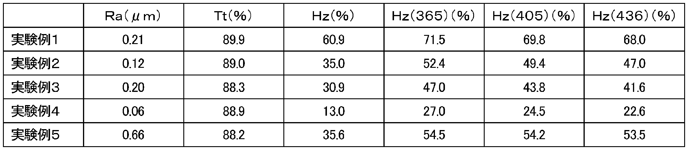
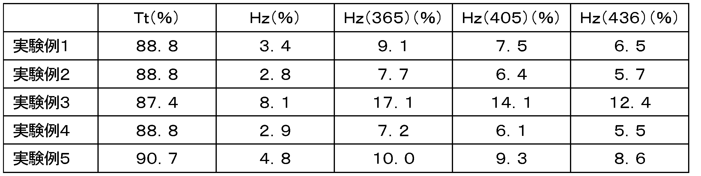
キャリアフィルムの第1の面上に、屈折率(nD)が1.56の透明樹脂(DIC株式会社製の商品名「アクリディックA807」(nD:1.54)と、三井化学株式会社製の商品名「タケネートD-110N」(nD:1.58)とを固形分比1:1で混合した樹脂)を用いて、厚さ25μmの透明樹脂層を設けた積層フィルムを作製した。積層フィルムの線透過率(Tt)、ヘーズ(Hz)、各波長における分光ヘーズをそれぞれ測定した。結果を表2に示す。
[感光性フィルムの作製]
(実施例1)
実験例1のキャリアフィルムの第1の面上に、屈折率(nD)が1.56の感光性樹脂組成物(日立化成株式会社製の商品名「SR7200G」)を塗布し、75℃で30分間乾燥して、厚さ25μmの感光層を形成することで、感光性フィルムを作製した。
(実施例1)
実験例1のキャリアフィルムの第1の面上に、屈折率(nD)が1.56の感光性樹脂組成物(日立化成株式会社製の商品名「SR7200G」)を塗布し、75℃で30分間乾燥して、厚さ25μmの感光層を形成することで、感光性フィルムを作製した。
(実施例2)
実験例2のキャリアフィルムを用いた以外は、実施例1と同様にして感光性フィルムを作製した。
実験例2のキャリアフィルムを用いた以外は、実施例1と同様にして感光性フィルムを作製した。
(比較例1)
実験例3のキャリアフィルムを用いた以外は、実施例1と同様にして感光性フィルムを作製した。
実験例3のキャリアフィルムを用いた以外は、実施例1と同様にして感光性フィルムを作製した。
(比較例2)
実験例4のキャリアフィルムを用いた以外は、実施例1と同様にして感光性フィルムを作製した。
実験例4のキャリアフィルムを用いた以外は、実施例1と同様にして感光性フィルムを作製した。
(比較例3)
実験例5のキャリアフィルムを用いた以外は、実施例1と同様にして感光性フィルムを作製した。
実験例5のキャリアフィルムを用いた以外は、実施例1と同様にして感光性フィルムを作製した。
[感光性フィルムの評価]
感光性フィルムの解像性及び密着性を下記条件で評価した。結果を表3に示す。
感光性フィルムの解像性及び密着性を下記条件で評価した。結果を表3に示す。
(解像性)
プレス熱板温度70℃、真空引き時間20秒、ラミネートプレス時間30秒、圧力0.4MPaの条件の下、基板上に、感光性フィルムの感光層が基板と接するように積層した評価用積層体を得た。次いで、キャリアフィルム上に、70μmの円形パターンを有するマスクを配置し、超高圧水銀ランプを光源とした平行露光機(株式会社清和光学製作所製の商品名「PA-1600H-150STP」)から300mJ/cm2の露光量で活性光線を照射した。照射後、キャリアフィルムを剥離し、現像液として30℃の1質量%炭酸ナトリウム水溶液を用いて、スプレー圧0.1MPaで60秒間スプレー現像を行い、レジストパターンを形成した。レジストパターンのビア開口径をマイクロスコープで測定することで解像性を評価した。
プレス熱板温度70℃、真空引き時間20秒、ラミネートプレス時間30秒、圧力0.4MPaの条件の下、基板上に、感光性フィルムの感光層が基板と接するように積層した評価用積層体を得た。次いで、キャリアフィルム上に、70μmの円形パターンを有するマスクを配置し、超高圧水銀ランプを光源とした平行露光機(株式会社清和光学製作所製の商品名「PA-1600H-150STP」)から300mJ/cm2の露光量で活性光線を照射した。照射後、キャリアフィルムを剥離し、現像液として30℃の1質量%炭酸ナトリウム水溶液を用いて、スプレー圧0.1MPaで60秒間スプレー現像を行い、レジストパターンを形成した。レジストパターンのビア開口径をマイクロスコープで測定することで解像性を評価した。
(密着性)
上記評価用積層体の全面に、パターンマスクを設けずに上記と同じ条件で活性光線を照射した後、キャリアフィルムを剥がして160℃で60分間加熱処理を行い、永久マスクレジストとなる硬化膜を作製した。次いで、硬化膜上にアンダーフィル材(日立化成株式会社製の商品名「CEL-C-3730S」)を塗布して、170℃、2時間で硬化させた。室温(25℃)における硬化膜とアンダーフィル材とのダイシェア強度をDAGE製の商品名「BT100」を用いて測定した。
上記評価用積層体の全面に、パターンマスクを設けずに上記と同じ条件で活性光線を照射した後、キャリアフィルムを剥がして160℃で60分間加熱処理を行い、永久マスクレジストとなる硬化膜を作製した。次いで、硬化膜上にアンダーフィル材(日立化成株式会社製の商品名「CEL-C-3730S」)を塗布して、170℃、2時間で硬化させた。室温(25℃)における硬化膜とアンダーフィル材とのダイシェア強度をDAGE製の商品名「BT100」を用いて測定した。

表1~3より、本発明の感光性フィルムは、特定の表面粗さと分光ヘーズとを有するキャリアフィルムを備えることで、解像性及び密着性に優れるレジストパターンを簡易に形成できることが確認された。
1…キャリアフィルム、1b…基材層、1a…樹脂層、2…感光層、4…レジストパターン、10…感光性フィルム、20…基板、30…フォトマスク。
Claims (5)
- 表面粗さが0.1~0.4μmの第1の面を有するキャリアフィルムと、前記第1の面上に形成された感光層と、を備える感光性フィルムであって、
前記キャリアフィルムは、ヘーズが30~65%であり、かつ、前記感光層の屈折率との差が±0.02以内の屈折率を有する透明樹脂層を、前記第1の面上に設けて測定される、405nmの波長における分光ヘーズが0.1~9.0%である、感光性フィルム。 - 前記キャリアフィルムが、前記第1の面側に無機粒子及びバインダー樹脂を含む樹脂層を有する、請求項1に記載の感光性フィルム。
- 前記樹脂層が、平均粒子径が0.1~3.0μmの無機粒子を含む、請求項2に記載の感光性フィルム。
- 前記樹脂層の厚さが、0.5~8μmである、請求項2又は3に記載の感光性フィルム。
- 請求項1~4のいずれか一項に記載の感光性フィルムを、前記感光層、前記キャリアフィルムの順に基板上に積層する工程と、
活性光線を、前記キャリアフィルムを介して前記感光層の所定部分に照射して、前記感光層に光硬化部を形成する工程と、
前記キャリアフィルムを剥離した後、前記光硬化部以外の部分を除去してレジストパターンを形成する工程と、を備え、
前記レジストパターンの表面粗さが0.1~0.4μmである、永久マスクレジストの形成方法。
Priority Applications (4)
| Application Number | Priority Date | Filing Date | Title |
|---|---|---|---|
| KR1020207035451A KR102697186B1 (ko) | 2018-05-16 | 2019-05-09 | 감광성 필름 및 영구 마스크 레지스트의 형성 방법 |
| US17/055,264 US12032292B2 (en) | 2018-05-16 | 2019-05-09 | Photosensitive film and method for forming permanent mask resist |
| CN201980032059.XA CN112352198B (zh) | 2018-05-16 | 2019-05-09 | 感光性膜及永久遮罩阻剂的形成方法 |
| JP2020519601A JP7345457B2 (ja) | 2018-05-16 | 2019-05-09 | 感光性フィルム及び永久マスクレジストの形成方法 |
Applications Claiming Priority (2)
| Application Number | Priority Date | Filing Date | Title |
|---|---|---|---|
| JP2018-094573 | 2018-05-16 | ||
| JP2018094573 | 2018-05-16 |
Publications (1)
| Publication Number | Publication Date |
|---|---|
| WO2019221012A1 true WO2019221012A1 (ja) | 2019-11-21 |
Family
ID=68540250
Family Applications (1)
| Application Number | Title | Priority Date | Filing Date |
|---|---|---|---|
| PCT/JP2019/018615 Ceased WO2019221012A1 (ja) | 2018-05-16 | 2019-05-09 | 感光性フィルム及び永久マスクレジストの形成方法 |
Country Status (6)
| Country | Link |
|---|---|
| US (1) | US12032292B2 (ja) |
| JP (1) | JP7345457B2 (ja) |
| KR (1) | KR102697186B1 (ja) |
| CN (1) | CN112352198B (ja) |
| TW (1) | TWI816793B (ja) |
| WO (1) | WO2019221012A1 (ja) |
Cited By (4)
| Publication number | Priority date | Publication date | Assignee | Title |
|---|---|---|---|---|
| KR20200139632A (ko) * | 2019-06-04 | 2020-12-14 | 다이요 잉키 세이조 가부시키가이샤 | 경화성 수지 조성물, 드라이 필름, 경화물, 및 프린트 배선판 |
| WO2022138246A1 (ja) * | 2020-12-25 | 2022-06-30 | 富士フイルム株式会社 | 転写材料及び積層体の製造方法 |
| TWI790919B (zh) * | 2021-02-17 | 2023-01-21 | 日商信越化學工業股份有限公司 | 負型阻劑材料及圖案形成方法 |
| TWI803190B (zh) * | 2021-02-17 | 2023-05-21 | 日商信越化學工業股份有限公司 | 正型阻劑材料及圖案形成方法 |
Citations (3)
| Publication number | Priority date | Publication date | Assignee | Title |
|---|---|---|---|---|
| JP2010085513A (ja) * | 2008-09-30 | 2010-04-15 | Toyo Ink Mfg Co Ltd | 感光性ドライフィルム |
| JP2012027368A (ja) * | 2010-07-27 | 2012-02-09 | Hitachi Chem Co Ltd | 感光性フィルム |
| JP2017191336A (ja) * | 2014-06-30 | 2017-10-19 | 太陽インキ製造株式会社 | 感光性ドライフィルムおよびそれを用いたプリント配線板の製造方法 |
Family Cites Families (10)
| Publication number | Priority date | Publication date | Assignee | Title |
|---|---|---|---|---|
| JP3789144B2 (ja) | 1994-06-14 | 2006-06-21 | 三菱化学ポリエステルフィルム株式会社 | フォトレジスト用積層ポリエステルフィルム |
| US8092980B2 (en) | 2007-01-31 | 2012-01-10 | Hitachi Chemical Company, Ltd. | Photosensitive element |
| KR101444044B1 (ko) * | 2010-12-16 | 2014-09-23 | 히타치가세이가부시끼가이샤 | 감광성 엘리먼트, 레지스트 패턴의 형성 방법 및 프린트 배선판의 제조 방법 |
| JP6014680B2 (ja) * | 2012-11-19 | 2016-10-25 | タツタ電線株式会社 | 積層フィルム及びシールドプリント配線板 |
| WO2014175312A1 (ja) * | 2013-04-26 | 2014-10-30 | 富士フイルム株式会社 | 転写材料、転写層付き基材及びタッチパネル、それらの製造方法、並びに情報表示装置 |
| KR102375653B1 (ko) | 2014-02-12 | 2022-03-16 | 쇼와덴코머티리얼즈가부시끼가이샤 | 감광성 엘리먼트 |
| TWI829181B (zh) * | 2014-04-25 | 2024-01-11 | 日商力森諾科股份有限公司 | 感光性元件、積層體、永久抗蝕罩幕及其製造方法以及半導體封裝的製造方法 |
| JP5882510B2 (ja) * | 2014-06-30 | 2016-03-09 | 太陽インキ製造株式会社 | 感光性ドライフィルムおよびそれを用いたプリント配線板の製造方法 |
| JP6750188B2 (ja) * | 2014-12-25 | 2020-09-02 | デクセリアルズ株式会社 | マスターフィルム付きナノ構造フィルム及びその製造方法 |
| JP7749969B2 (ja) | 2020-09-18 | 2025-10-07 | 株式会社大阪ソーダ | 化粧シートおよび化粧板 |
-
2019
- 2019-05-09 CN CN201980032059.XA patent/CN112352198B/zh active Active
- 2019-05-09 WO PCT/JP2019/018615 patent/WO2019221012A1/ja not_active Ceased
- 2019-05-09 JP JP2020519601A patent/JP7345457B2/ja active Active
- 2019-05-09 KR KR1020207035451A patent/KR102697186B1/ko active Active
- 2019-05-09 US US17/055,264 patent/US12032292B2/en active Active
- 2019-05-16 TW TW108116872A patent/TWI816793B/zh active
Patent Citations (3)
| Publication number | Priority date | Publication date | Assignee | Title |
|---|---|---|---|---|
| JP2010085513A (ja) * | 2008-09-30 | 2010-04-15 | Toyo Ink Mfg Co Ltd | 感光性ドライフィルム |
| JP2012027368A (ja) * | 2010-07-27 | 2012-02-09 | Hitachi Chem Co Ltd | 感光性フィルム |
| JP2017191336A (ja) * | 2014-06-30 | 2017-10-19 | 太陽インキ製造株式会社 | 感光性ドライフィルムおよびそれを用いたプリント配線板の製造方法 |
Cited By (9)
| Publication number | Priority date | Publication date | Assignee | Title |
|---|---|---|---|---|
| KR20200139632A (ko) * | 2019-06-04 | 2020-12-14 | 다이요 잉키 세이조 가부시키가이샤 | 경화성 수지 조성물, 드라이 필름, 경화물, 및 프린트 배선판 |
| JP2020200449A (ja) * | 2019-06-04 | 2020-12-17 | 太陽インキ製造株式会社 | 硬化性樹脂組成物、ドライフィルム、硬化物、およびプリント配線板 |
| JP2024133135A (ja) * | 2019-06-04 | 2024-10-01 | 太陽ホールディングス株式会社 | 硬化性樹脂組成物、ドライフィルム、硬化物、およびプリント配線板 |
| JP7610928B2 (ja) | 2019-06-04 | 2025-01-09 | 太陽ホールディングス株式会社 | 硬化性樹脂組成物、ドライフィルム、硬化物、およびプリント配線板 |
| KR102846500B1 (ko) | 2019-06-04 | 2025-08-18 | 다이요 홀딩스 가부시키가이샤 | 경화성 수지 조성물, 드라이 필름, 경화물, 및 프린트 배선판 |
| WO2022138246A1 (ja) * | 2020-12-25 | 2022-06-30 | 富士フイルム株式会社 | 転写材料及び積層体の製造方法 |
| JPWO2022138246A1 (ja) * | 2020-12-25 | 2022-06-30 | ||
| TWI790919B (zh) * | 2021-02-17 | 2023-01-21 | 日商信越化學工業股份有限公司 | 負型阻劑材料及圖案形成方法 |
| TWI803190B (zh) * | 2021-02-17 | 2023-05-21 | 日商信越化學工業股份有限公司 | 正型阻劑材料及圖案形成方法 |
Also Published As
| Publication number | Publication date |
|---|---|
| KR102697186B1 (ko) | 2024-08-22 |
| JP7345457B2 (ja) | 2023-09-15 |
| US12032292B2 (en) | 2024-07-09 |
| TWI816793B (zh) | 2023-10-01 |
| US20210124267A1 (en) | 2021-04-29 |
| CN112352198B (zh) | 2024-08-16 |
| JPWO2019221012A1 (ja) | 2021-06-17 |
| CN112352198A (zh) | 2021-02-09 |
| KR20210039332A (ko) | 2021-04-09 |
| TW201947319A (zh) | 2019-12-16 |
Similar Documents
| Publication | Publication Date | Title |
|---|---|---|
| JP6879348B2 (ja) | 感光性エレメント、積層体、永久マスクレジスト及びその製造方法並びに半導体パッケージの製造方法 | |
| TWI584070B (zh) | 感光性樹脂組成物、感光性膜、永久遮罩抗蝕劑及永久遮罩抗蝕劑的製造方法 | |
| JP5472692B2 (ja) | アルカリ現像可能な感光性樹脂組成物及びそれを用いた感光性フィルム | |
| JP6143090B2 (ja) | 感光性樹脂組成物、これを用いた感光性フィルム、永久レジスト及び永久レジストの製造方法 | |
| JP7345457B2 (ja) | 感光性フィルム及び永久マスクレジストの形成方法 | |
| JP5582348B2 (ja) | 感光性樹脂組成物及び感光性フィルム | |
| JP5641293B2 (ja) | 感光性樹脂組成物及び感光性フィルム、永久レジスト | |
| JP5768495B2 (ja) | 感光性樹脂組成物、感光性エレメント及び永久レジスト | |
| JP2011048313A (ja) | 感光性樹脂組成物及び感光性フィルム | |
| KR102319223B1 (ko) | 감광성 수지 조성물, 해당 감광성 수지 조성물을 사용한 솔더 레지스트 필름, 플렉시블 프린트 배선판 및 화상 표시 장치 | |
| JPWO2019188861A1 (ja) | 黒色構造体、ならびにそれを備えた自発光画像表示装置 | |
| JP5990366B2 (ja) | 積層体及びそれを用いたロール | |
| JP2008015285A (ja) | 感光性熱硬化性樹脂組成物 | |
| JP5804336B2 (ja) | 感光性樹脂組成物及び感光性フィルム、永久レジスト | |
| CN109388026A (zh) | 光致抗蚀膜、抗蚀图案的形成方法及导体图案的形成方法 | |
| JP4910610B2 (ja) | 感光性樹脂組成物及び感光性フィルム | |
| JP4259170B2 (ja) | 感光性樹脂組成物、これを用いた感光性エレメント、レジストパターンの形成方法及びプリント配線板の製造方法 | |
| TW483294B (en) | Laminate for pattern formation | |
| JPWO2005071487A1 (ja) | 感光性フィルム及びそれを用いたプリント配線板の製造方法 |
Legal Events
| Date | Code | Title | Description |
|---|---|---|---|
| 121 | Ep: the epo has been informed by wipo that ep was designated in this application |
Ref document number: 19803627 Country of ref document: EP Kind code of ref document: A1 |
|
| ENP | Entry into the national phase |
Ref document number: 2020519601 Country of ref document: JP Kind code of ref document: A |
|
| NENP | Non-entry into the national phase |
Ref country code: DE |
|
| 122 | Ep: pct application non-entry in european phase |
Ref document number: 19803627 Country of ref document: EP Kind code of ref document: A1 |