WO2019181495A1 - 制御装置、制御方法及びコンピュータプログラム - Google Patents
制御装置、制御方法及びコンピュータプログラム Download PDFInfo
- Publication number
- WO2019181495A1 WO2019181495A1 PCT/JP2019/008780 JP2019008780W WO2019181495A1 WO 2019181495 A1 WO2019181495 A1 WO 2019181495A1 JP 2019008780 W JP2019008780 W JP 2019008780W WO 2019181495 A1 WO2019181495 A1 WO 2019181495A1
- Authority
- WO
- WIPO (PCT)
- Prior art keywords
- switch
- resistor
- voltage value
- circuit
- voltage
- Prior art date
- Legal status (The legal status is an assumption and is not a legal conclusion. Google has not performed a legal analysis and makes no representation as to the accuracy of the status listed.)
- Ceased
Links
Images


Classifications
-
- H—ELECTRICITY
- H03—ELECTRONIC CIRCUITRY
- H03K—PULSE TECHNIQUE
- H03K17/00—Electronic switching or gating, i.e. not by contact-making and –breaking
- H03K17/08—Modifications for protecting switching circuit against overcurrent or overvoltage
- H03K17/081—Modifications for protecting switching circuit against overcurrent or overvoltage without feedback from the output circuit to the control circuit
- H03K17/08116—Modifications for protecting switching circuit against overcurrent or overvoltage without feedback from the output circuit to the control circuit in composite switches
-
- H—ELECTRICITY
- H03—ELECTRONIC CIRCUITRY
- H03K—PULSE TECHNIQUE
- H03K17/00—Electronic switching or gating, i.e. not by contact-making and –breaking
- H03K17/08—Modifications for protecting switching circuit against overcurrent or overvoltage
- H03K17/082—Modifications for protecting switching circuit against overcurrent or overvoltage by feedback from the output to the control circuit
- H03K17/0822—Modifications for protecting switching circuit against overcurrent or overvoltage by feedback from the output to the control circuit in field-effect transistor switches
-
- H—ELECTRICITY
- H02—GENERATION; CONVERSION OR DISTRIBUTION OF ELECTRIC POWER
- H02H—EMERGENCY PROTECTIVE CIRCUIT ARRANGEMENTS
- H02H3/00—Emergency protective circuit arrangements for automatic disconnection directly responsive to an undesired change from normal electric working condition with or without subsequent reconnection ; integrated protection
- H02H3/08—Emergency protective circuit arrangements for automatic disconnection directly responsive to an undesired change from normal electric working condition with or without subsequent reconnection ; integrated protection responsive to excess current
- H02H3/087—Emergency protective circuit arrangements for automatic disconnection directly responsive to an undesired change from normal electric working condition with or without subsequent reconnection ; integrated protection responsive to excess current for DC applications
-
- H—ELECTRICITY
- H02—GENERATION; CONVERSION OR DISTRIBUTION OF ELECTRIC POWER
- H02J—ELECTRIC POWER NETWORKS; CIRCUIT ARRANGEMENTS OR SYSTEMS FOR SUPPLYING OR DISTRIBUTING ELECTRIC POWER; SYSTEMS FOR STORING ELECTRIC ENERGY
- H02J7/00—Circuit arrangements for charging or discharging batteries or for supplying loads from batteries
- H02J7/50—Circuit arrangements for charging or discharging batteries or for supplying loads from batteries acting upon multiple batteries simultaneously or sequentially
- H02J7/575—Parallel/serial switching of connection of batteries to charge or load circuit
-
- H—ELECTRICITY
- H02—GENERATION; CONVERSION OR DISTRIBUTION OF ELECTRIC POWER
- H02J—ELECTRIC POWER NETWORKS; CIRCUIT ARRANGEMENTS OR SYSTEMS FOR SUPPLYING OR DISTRIBUTING ELECTRIC POWER; SYSTEMS FOR STORING ELECTRIC ENERGY
- H02J7/00—Circuit arrangements for charging or discharging batteries or for supplying loads from batteries
- H02J7/60—Circuit arrangements for charging or discharging batteries or for supplying loads from batteries including safety or protection arrangements
- H02J7/663—Circuit arrangements for charging or discharging batteries or for supplying loads from batteries including safety or protection arrangements using battery or load disconnect circuits
-
- H—ELECTRICITY
- H02—GENERATION; CONVERSION OR DISTRIBUTION OF ELECTRIC POWER
- H02J—ELECTRIC POWER NETWORKS; CIRCUIT ARRANGEMENTS OR SYSTEMS FOR SUPPLYING OR DISTRIBUTING ELECTRIC POWER; SYSTEMS FOR STORING ELECTRIC ENERGY
- H02J7/00—Circuit arrangements for charging or discharging batteries or for supplying loads from batteries
- H02J7/855—Circuit arrangements for charging or discharging batteries or for supplying loads from batteries with circuits adapted for supplying loads from the battery
-
- H—ELECTRICITY
- H03—ELECTRONIC CIRCUITRY
- H03K—PULSE TECHNIQUE
- H03K17/00—Electronic switching or gating, i.e. not by contact-making and –breaking
- H03K17/002—Switching arrangements with several input- or output terminals
-
- H—ELECTRICITY
- H03—ELECTRONIC CIRCUITRY
- H03K—PULSE TECHNIQUE
- H03K17/00—Electronic switching or gating, i.e. not by contact-making and –breaking
- H03K17/12—Modifications for increasing the maximum permissible switched current
- H03K17/122—Modifications for increasing the maximum permissible switched current in field-effect transistor switches
Definitions
- the present invention relates to a control device, a control method, and a computer program.
- This application claims priority based on Japanese Patent Application No. 2018-056897 filed on Mar. 23, 2018, and incorporates all the description content described in the above Japanese application.
- Patent Document 1 discloses a control device that controls power supply from a vehicle battery to a load.
- this control device one end of each of the two semiconductor switches is connected to the positive electrode of the battery.
- the other end of each of the two semiconductor switches is connected to one end of a load.
- the negative electrode of the battery and the other end of the load are grounded.
- a control device includes a first series circuit having a first switch and a first resistor connected in series, a second switch and a second resistor connected in series, and the first switch A voltage value corresponding to a voltage value between both ends of the first resistor, a second series circuit connected in parallel to the series circuit, an instruction unit for instructing to turn on the first switch and the second switch, A voltage output circuit for outputting, and the first switch based on a voltage value output by the voltage output circuit when the instruction unit instructs to turn on the first switch and the second switch.
- the control method includes a step of instructing to turn on a first switch connected in series to a first resistor and a second switch connected in series to a second resistor; Based on the acquired voltage value in the step of acquiring a voltage value corresponding to the voltage value between both ends of the first resistor and instructing to switch on to the first switch and the second switch. Detecting the occurrence of a failure in at least one of the first switch, the second switch, the first resistor, and the second resistor, and the first series circuit having the first switch and the first resistor comprises: The second switch and the second series circuit having the second resistor are connected in parallel.
- the computer program instructs the computer to turn on a first switch connected in series to the first resistor and a second switch connected in series to the second resistor. And a step of acquiring a voltage value corresponding to a voltage value between both ends of the first resistor, and an acquired voltage value when instructing to turn on the first switch and the second switch. And detecting the occurrence of a failure in at least one of the first switch, the second switch, the first resistor and the second resistor, based on the first switch and the first switch.
- a first series circuit having a resistor is connected in parallel to the second switch and a second series circuit having a second resistor.
- the present invention can be realized not only as a control device including such a characteristic processing unit, but also as a control method using such characteristic processing as a step, or causing a computer to execute such a step. Or as a computer program. Further, the present invention can be realized as a semiconductor integrated circuit that realizes part or all of the control device, or as a power supply system including the control device.
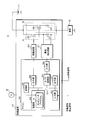
- FIG. 1 is a block diagram illustrating a main configuration of a power supply system according to Embodiment 1.
- FIG. It is a circuit diagram of a current detection circuit. It is explanatory drawing of the phenomenon which arises by failure. It is a flowchart which shows the procedure of a failure detection process. It is a block diagram which shows the principal part structure of the power supply system in Embodiment 2.
- FIG. It is explanatory drawing of the phenomenon which arises by failure. It is a flowchart which shows the procedure of a failure detection process. It is a flowchart which shows the procedure of a failure detection process. It is a block diagram which shows the principal part structure of the power supply system in Embodiment 3.
- FIG. It is a block diagram which shows the principal part structure of a microcomputer.
- Patent Document 1 it is assumed that one of the two semiconductor switches has failed and is fixed off. In this case, when the other semiconductor switch is switched on, a large current flows through the other semiconductor switch. When a large current flows through the other semiconductor switch, a large amount of power is consumed by the other semiconductor switch. As a result, the temperature of the other semiconductor switch rises to an abnormal temperature, and the other semiconductor switch may also fail.
- a control device includes a first switch having a first switch and a first resistor connected in series, a second switch and a second resistor connected in series, According to a voltage value between both ends of the first resistor, a second series circuit connected in parallel to the first series circuit, an instruction unit instructing to turn on the first switch and the second switch, and A voltage output circuit that outputs a voltage value; and when the instruction unit instructs to turn on the first switch and the second switch, based on the voltage value output by the voltage output circuit, A first switch, a second switch, a first resistor, and a detection unit that detects occurrence of a failure in at least one of the second resistors.
- the voltage value output from the voltage output circuit increases when the voltage value across the first resistor increases
- the detection unit includes the voltage When the voltage value output by the output circuit is less than the first threshold, the occurrence of a failure in at least one of the first switch, the first resistor, and the second resistor is detected, and the voltage output by the voltage output circuit When the value is greater than or equal to a second threshold, it is detected that a failure has occurred in at least one of the second switch, the first resistor, and the second resistor, and the first threshold is less than the second threshold.
- the control device includes a voltage detection circuit that detects a voltage value of a connection node between the first switch and the first resistor, and the detection unit includes the first switch, the first switch, and the first switch.
- the detection unit includes the first switch, the first switch, and the first switch.
- the control device includes a second voltage detection circuit that detects a voltage value of a connection node between the second switch and the second resistor, and the detection unit includes the second switch.
- the detection unit includes the second switch.
- current flows in the order of the first switch and the first resistor, and the voltage output circuit receives current from a connection node between the first switch and the first resistor.
- the current output unit that draws in and outputs the drawn current and a current resistor through which the current output from the current output unit flows, and the voltage output circuit outputs a voltage value across the current resistor.
- the control method is a step of instructing to turn on the first switch connected in series to the first resistor and the second switch connected in series to the second resistor. And a step of acquiring a voltage value corresponding to a voltage value between both ends of the first resistor, and an acquired voltage value when instructing to turn on the first switch and the second switch. And detecting the occurrence of a failure in at least one of the first switch, the second switch, the first resistor, and the second resistor, the first switch having the first switch and the first resistor.
- the series circuit is connected in parallel to the second series circuit having the second switch and the second resistor.
- a computer program turns on a first switch connected in series to a first resistor and a second switch connected in series to a second resistor. Obtaining in the step of instructing, obtaining the voltage value according to the voltage value between both ends of the first resistor, and instructing to switch on to the first switch and the second switch And detecting the occurrence of a failure in at least one of the first switch, the second switch, the first resistor, and the second resistor based on the voltage value, and the first switch The first series circuit having the first resistor is connected in parallel to the second switch and the second series circuit having the second resistor.
- the voltage value across the first resistor includes the first series circuit and the second series circuit. This is the voltage value across the parallel circuit.
- the parallel circuit In the case where the first switch and the second switch are instructed to be turned on, when the second switch is fixed to be off, or when the first resistor or the second resistor is open, the parallel circuit And the voltage value across the first resistor is large.
- the first switch When the first switch and the second switch are instructed to be switched on, the first switch is fixed when the first switch is fixed off or the first resistor or the second resistor is short-circuited.
- the voltage value across the resistor is zero volts.
- the voltage output circuit outputs a voltage value corresponding to the voltage value across the first resistor.
- the first switch or the second switch When the first switch or the second switch is fixed to be off, the voltage value output from the voltage output unit varies greatly. Thereby, the occurrence of a failure in at least one of the first switch, the second switch, the first resistor, and the second resistor is detected.
- the failure of at least one of the first switch, the first resistor, and the second resistor is detected. Detect occurrence.
- the voltage value output from the voltage output unit is equal to or greater than the second threshold, the occurrence of a failure in at least one of the second switch, the first resistor, and the second resistor is detected.
- FIG. 1 is a block diagram illustrating a main configuration of a power supply system 1 according to the first embodiment.
- the power supply system 1 is suitably mounted on a vehicle and includes a control device 10, a battery 11, and a load 12.
- the control device 10 is connected to the positive electrode of the battery 11 and one end of the load 12.
- the negative electrode of the battery 11 and the other end of the load 12 are grounded.
- the load 12 is an electric device mounted on the vehicle. When power is supplied to the load 12, the load 12 operates. When power supply to the load 12 stops, the load 12 stops operating.
- the control device 10 receives an operation signal for instructing the operation of the load 12 and a stop signal for instructing the operation of the load 12 to stop.
- the control device 10 electrically connects the positive electrode of the battery 11 and one end of the load 12. Accordingly, the battery 11 supplies power to the load 12 via the control device 10.
- the control device 10 interrupts the electrical connection between the battery 11 and the load 12. Thereby, the power supply from the battery 11 to the load 12 is stopped, and the load 12 stops its operation. As described above, the control device 10 controls power feeding from the battery 11 to the load 12 by electrically connecting the battery 11 and the load 12 and blocking the electrical connection.
- control device 10 detects the occurrence of the failure and outputs a notification signal for notifying the occurrence of the failure to a device (not shown). Thereby, for example, lighting of a lamp or display of a message is performed in the vehicle, and the occurrence of the failure is notified to the vehicle occupant.
- the control device 10 includes a drive circuit 20, a current detection circuit 21, a microcomputer (hereinafter referred to as a microcomputer) 22, a first series circuit A, and a second series circuit B.
- the microcomputer 22 includes output units 50 and 51, input units 52 and 53, an A / D conversion unit 54, a storage unit 55, and a control unit 56.
- the first series circuit A includes a first switch 30 and a first resistor 31.
- the second series circuit B includes a second switch 40 and a second resistor 41.
- Each of the first switch 30 and the second switch 40 is an N-channel FET (Field-Effect-Transistor).
- the first resistor 31 a resistance element or a resistance of a pattern (conductive foil) formed on the substrate is used.
- the second resistor 41 a resistive element or a resistor of a pattern formed on the substrate is used.
- the second series circuit B is connected to the first series circuit A in parallel.
- the first switch 30 and the first resistor 31 are connected in series.
- the source of the first switch 30 is connected to one end of the first resistor 31.
- the second switch 40 is connected to the second resistor 41 in series.
- the source of the second switch 40 is connected to one end of the second resistor 41.
- the drains of the first switch 30 and the second switch 40 are connected to the positive electrode of the battery 11.
- the other ends of the first resistor 31 and the second resistor 41 are connected to one end of the load 12.
- the gates of the first switch 30 and the second switch 40 are connected to the output terminal of the drive circuit 20.
- the input end of the drive circuit 20 is connected to the output unit 50 of the microcomputer 22. Both ends of the first resistor 31 are connected to the current detection circuit 21.
- the current detection circuit 21 is further connected to the input unit 52 of the microcomputer 22.
- the input unit 52 is further connected to an A / D conversion unit 54.
- the output units 50 and 51, the input unit 53, the A / D conversion unit 54, the storage unit 55, and the control unit 56 are connected to an internal bus 57.
- each of the first switch 30 and the second switch 40 when the gate voltage value based on the source potential is equal to or higher than a certain ON threshold, current can flow through the drain and source. At this time, each of the first switch 30 and the second switch 40 is on. In addition, when the gate voltage relative to the source potential is less than a certain off threshold, no current flows through the drain and the source. At this time, each of the first switch 30 and the second switch 40 is on. For each of the first switch 30 and the second switch 40, the ON threshold value exceeds the OFF threshold value.
- the output unit 50 outputs a high level voltage or a low level voltage to the drive circuit 20.
- the output unit 50 switches the voltage output to the drive circuit 20 to a high level voltage or a low level voltage in accordance with an instruction from the control unit 56.
- the drive circuit 20 increases the voltage values of the gates of the first switch 30 and the second switch 40 with respect to the ground potential.
- the gate voltage value based on the source potential becomes the on threshold value or more, and the first switch 30 and the second switch 40 are turned on.
- the first switch 30 and the second switch 40 are switched on, the positive electrode of the battery 11 and one end of the load 12 are electrically connected, power is supplied from the battery 11 to the load 12, and the load 12 operates. .
- the resistance values of the first resistor 31 and the second resistor 41 preferably match.
- the current values of the currents flowing through the first series circuit A and the second series circuit B are substantially the same, and the deterioration rates of the first switch 30 and the second switch 40 are substantially the same.
- One of the first switch 30 and the second switch 40 is prevented from rapidly deteriorating.
- the drive circuit 20 reduces the voltage values of the gates of the first switch 30 and the second switch 40 with respect to the ground potential. Let Thereby, in each of the first switch 30 and the second switch 40, the gate voltage value based on the source potential becomes less than the off threshold, and the first switch 30 and the second switch 40 are turned off.
- the drive circuit 20 turns on or off the first switch 30 and the second switch 40 by adjusting the voltage values of the gates of the first switch 30 and the second switch 40 with reference to the ground potential. Switch.
- the resistance value between the drain and the source is considered to be zero ohms.
- the resistance value between the drain and the source is considered to be infinite.
- the current detection circuit 21 outputs an analog voltage value proportional to the voltage value across the first resistor 31 to the input unit 52 of the microcomputer 22.
- the voltage value output from the current detection circuit 21 is referred to as a resistance voltage value.
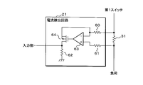
- FIG. 2 is a circuit diagram of the current detection circuit 21.
- the current detection circuit 21 includes circuit resistors 60, 61, 62, a differential amplifier 63, and a P-channel type FET 64.
- the differential amplifier 63 is a so-called operational amplifier, and has a plus end, a minus end, and an output end.
- One end of the circuit resistor 60 is connected to one end of the first resistor 31 on the first switch 30 side.
- One end of the circuit resistor 61 is connected to one end of the first resistor 31 on the load 12 side.
- the other ends of the circuit resistors 60 and 61 are connected to the positive end and the negative end of the differential amplifier 63.
- the other end of the circuit resistor 60 is further connected to the source of the FET 64.
- the output terminal of the differential amplifier 63 is connected to the gate of the FET 64.
- the drain of the FET 64 is connected to the input unit 52 of the microcomputer 22 and one end of the circuit resistor 62.
- the other end of the circuit resistor 62 is grounded.
- FET64 functions as a variable resistor.
- a current flows through the drain and the source.
- the lower the gate voltage value relative to the source potential is, the smaller the resistance value between the drain and the source is.
- the first switch 30 When the first switch 30 is on, current flows from the positive electrode of the battery 11 in the order of the first switch 30, the circuit resistor 60, the FET 64, and the circuit resistor 62.
- the current value of the current flowing through the circuit resistor 62 is larger as the resistance value between the drain and source of the FET 64 is smaller.
- a voltage value across the circuit resistor 62 is output to the input unit 52 of the microcomputer 22 as a resistance voltage value.
- the voltage value between both ends of the circuit resistor 62 is larger as the current value of the current flowing through the circuit resistor 62 is larger.
- the FET 64 draws a current from the connection node between the first switch 30 and the first resistor 31, and outputs the drawn current.
- the current output from the FET 64 flows through the circuit resistor 62.
- the current detection circuit 21, the FET 64, and the circuit resistor 62 function as a voltage output circuit, a current output unit, and a current resistor, respectively.
- the differential amplifier 63 adjusts the voltage value of the gate of the FET 64 with reference to the ground potential.
- the differential amplifier 63 decreases the voltage value of the gate of the FET 64 with respect to the ground potential as the voltage value across the first resistor 31 increases.
- the lower the gate voltage value based on the ground potential the lower the gate voltage value based on the source potential.
- the lower the gate voltage value with respect to the source potential the smaller the resistance value between the drain and the source.
- the differential amplifier 63 decreases the voltage value of the gate of the FET 64.
- the resistance value between the drain and source of the FET 64 decreases, and the current value of the current flowing through the circuit resistor 62 increases.
- the voltage value across the circuit resistor 62 increases.
- the differential amplifier 63 increases the voltage value of the gate of the FET 64.
- the resistance value between the drain and source of the FET 64 increases, and the current value of the current flowing through the circuit resistor 62 decreases.
- the voltage value across the circuit resistor 62 decreases.
- the resistance values of the circuit resistors 60 and 62 are denoted as r60 and r62, respectively.
- a voltage value across the first resistor 31 is referred to as V31.
- the resistance voltage value that is, the voltage value between both ends of the circuit resistance 62 is described as V62.
- the current value of the current flowing through the load 12 is denoted as It.
- the combined resistance value of the parallel circuit of the first series circuit A and the second series circuit B is described as rs.
- the voltage value V31 across the first resistor 31 is expressed by the following equation (2).
- V31 rs ⁇ It (2)
- the analog resistance voltage value is input from the current detection circuit 21 to the input unit 52 of the microcomputer 22.
- the input unit 52 outputs the input analog resistance voltage value to the A / D conversion unit 54.
- the A / D conversion unit 54 converts the analog resistance voltage value input from the input unit 52 into a digital resistance voltage value.
- the control unit 56 acquires a digital resistance voltage value from the A / D conversion unit 54.
- the output unit 51 outputs a notification signal to a device (not shown) according to an instruction from the control unit 56.
- An operation signal and a stop signal are input to the input unit 53.
- the input unit 53 notifies the control unit 56 of the input signal.
- the storage unit 55 is a nonvolatile memory.
- the storage unit 55 stores a computer program P.
- the control unit 56 has one or more CPUs (Central Processing Unit). One or a plurality of CPUs included in the control unit 56 executes the computer program P to execute an operation process, a stop process, a protection process, and a failure detection process.
- the operation process is a process for operating the load 12.
- the stop process is a process for stopping the operation of the load 12.
- the protection process is a process for protecting the load 12 from overcurrent.
- the failure detection process is a process for detecting the occurrence of a failure.
- the computer program P is used to cause one or a plurality of CPUs included in the control unit 56 to execute an operation process, a stop process, a protection process, and a failure detection process.
- the computer program P may be stored in the storage medium E so that it can be read by one or more CPUs included in the control unit 56.
- the computer program P read from the storage medium E by a reading device (not shown) is stored in the storage unit 55.
- the storage medium E is an optical disk, a flexible disk, a magnetic disk, a magnetic optical disk, a semiconductor memory, or the like.
- the optical disc is a CD (Compact Disc) -ROM (Read Only Memory), a DVD (Digital Versatile Disc) -ROM, or a BD (Blu-ray (registered trademark) Disc).
- the magnetic disk is, for example, a hard disk.
- the computer program P may be downloaded from an external device (not shown) connected to a communication network (not shown), and the downloaded computer program P may be stored in the storage unit 55.
- the control unit 56 executes an operation process when an operation signal is input to the input unit 53.
- the control unit 56 instructs the output unit 50 to switch to the high level voltage.
- the output unit 50 switches the voltage output to the drive circuit 20 to the high level voltage, and the drive circuit 20 switches the first switch 30 and the second switch 40 on. Therefore, instructing the output unit 50 to switch to the high level voltage corresponds to instructing the drive circuit 20 to switch on the first switch 30 and the second switch 40.
- the control unit 56 functions as an instruction unit.
- the control unit 56 ends the operation process.
- the control unit 56 executes a stop process.
- the control unit 56 instructs the output unit 50 to switch to the low level voltage.
- the output unit 50 switches the voltage output to the drive circuit 20 to the low level voltage, and the drive circuit 20 switches the first switch 30 and the second switch 40 to OFF.
- instructing the output unit 50 to switch to the low level voltage corresponds to instructing the drive circuit 20 to switch the first switch 30 and the second switch 40 to OFF.
- the control unit 56 ends the stop process.
- control unit 56 When the control unit 56 instructs the output unit 50 to switch to the high-level voltage, that is, when the drive circuit 20 instructs the switch to turn on the first switch 30 and the second switch 40, Perform protection processing periodically.
- the control unit 56 acquires the resistance voltage value from the A / D conversion unit 54, and calculates the current value of the current flowing through the load 12 by substituting the acquired resistance voltage value into the equation (3). .
- the control unit 56 determines whether or not the calculated current value is equal to or greater than a predetermined current value.
- control unit 56 determines that the calculated current value is equal to or greater than the predetermined current value
- the control unit 56 instructs the output unit 50 to switch to the low level voltage.
- the output unit 50 switches the voltage output to the drive circuit 20 to the low level voltage
- the drive circuit 20 switches the first switch 30 and the second switch 40 to OFF.
- an overcurrent is prevented from flowing through the load 12.
- the control unit 56 ends the protection process.
- the control unit 56 also ends the protection process when determining that the calculated current value is less than the predetermined current value.
- the failure detection process is executed periodically.
- the control unit 56 uses the resistance voltage value output from the current detection circuit 21 to the input unit 52 in the first switch 30, the first resistor 31, the second switch 40, and the second resistor 41. The occurrence of a failure in at least one of the above is detected.
- FIG. 3 is an explanatory diagram of a phenomenon caused by a failure.
- a failure in which the switch is fixed off or a failure in which both ends of the resistor are opened is referred to as an open failure.
- a failure in which both ends of the resistor are short-circuited is described as a short-circuit failure.
- a lower threshold value and an upper threshold value are set as threshold values related to the resistance voltage value. The lower threshold is less than the upper threshold and exceeds zero.
- the control unit 56 performs the failure detection process in a state in which the drive circuit 20 is instructed to turn on the first switch 30 and the second switch 40.
- the first switch 30 When an open failure occurs in the first switch 30, no current flows through the first resistor 31. For this reason, the voltage value across the first resistor 31 is zero V, and the resistance voltage value is zero V. Further, when a short circuit failure occurs in the first resistor 31 or the second resistor 41, a current flows from the battery 11 to the load 12. However, since no voltage drop occurs between both ends of the first resistor 31, the voltage value between both ends of the first resistor 31 is zero V, and the resistance voltage value is zero V.
- the resistance voltage value is zero V, which is less than the lower threshold value. It is.
- the output voltage value of the battery 11 (hereinafter referred to as the battery voltage value) is described as Vb.
- a combined resistance value of a parallel circuit in which the second resistor 41 is connected in parallel to the first resistor 31 is described as rp.
- the resistance value of the load 12 is described as r12.
- the control unit 56 instructs the drive circuit 20 to turn on the first switch 30 and the second switch 40. Therefore, the resistance value between both ends of the first resistor 31 is usually a combined resistance value of a parallel circuit in which the second resistor 41 is connected in parallel to the first resistor 31.
- the voltage value V31 between both ends of the first resistor 31 is represented by Vb ⁇ rp / (rp + r12).
- the resistance value of the first resistor 31 is described as r31.
- the resistance value between both ends of the first resistor 31 is the resistance value r31 of the first resistor 31.
- the voltage value V31 across the first resistor 31 is expressed by Vb ⁇ r31 / (r12 + r31).
- the resistance value r31 exceeds the resistance value rp. For this reason, Vb ⁇ r31 / (r12 + r31) exceeds Vb ⁇ rp / (rp + r12).
- the resistance value of the second resistor 41 is described as r41.
- the resistance value between both ends of the first resistor 31 is the resistance value r ⁇ b> 41 of the second resistor 41.
- the voltage value V31 across the first resistor 31 is represented by Vb ⁇ r41 / (r12 + r41).
- the resistance value r41 exceeds the resistance value rp. For this reason, Vb ⁇ r41 / (r12 + r41) exceeds Vb ⁇ rp / (rp + r12).
- the resistance voltage value V62 is proportional to the voltage value V31 across the first resistor 31 as shown in the equation (1).
- the upper threshold value is set to a voltage value that is equal to or lower than a low voltage value in the resistance voltage value when an open circuit failure occurs in each of the first resistor 31 and the second resistor 41 and higher than the resistance voltage value in the normal state. ing. For this reason, when an open failure occurs in the second switch 40, the first resistor 31, or the second resistor 41, the resistance voltage value is equal to or higher than the upper threshold value.
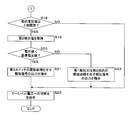
- FIG. 4 is a flowchart showing a procedure of failure detection processing. As described above, the control unit 56 periodically executes the failure detection process when the drive circuit 20 is instructed to switch on.
- the control unit 56 acquires a resistance voltage value from the A / D conversion unit 54 (step S1), and determines whether or not the acquired resistance voltage value is less than a lower threshold (step S1). S2). As described above, when the resistance voltage value is less than the lower threshold, a failure has occurred in at least one of the first switch 30, the first resistor 31, and the second resistor 41. Accordingly, determining that the resistance voltage value is less than the lower threshold corresponds to detecting the occurrence of a failure in at least one of the first switch 30, the first resistor 31, and the second resistor 41. The lower threshold corresponds to the first threshold.
- the control unit 56 also functions as a detection unit.
- Step S3 the control unit 56 determines whether or not the resistance voltage value acquired in Step S1 is equal to or higher than the upper threshold value (Step S3).
- the control unit 56 determines whether or not the resistance voltage value acquired in Step S1 is equal to or higher than the upper threshold value (Step S3).
- the resistance voltage value is equal to or higher than the upper threshold value, at least one of the second switch 40, the first resistor 31, and the second resistor 41 is out of order. Therefore, determining that the resistance voltage value is equal to or greater than the upper threshold corresponds to detecting the occurrence of a failure in at least one of the second switch 40, the first resistor 31, and the second resistor 41.
- the upper threshold corresponds to the second threshold.
- the control unit 56 When determining that the resistance voltage value is less than the lower threshold value (S2: YES), or when determining that the resistance voltage value is greater than or equal to the upper threshold value (S3: YES), the control unit 56 outputs to the output unit 50.
- the switching to the low level voltage is instructed (step S4). Accordingly, the output unit 50 switches the voltage output to the drive circuit 20 to the low level voltage, and the drive circuit 20 switches the first switch 30 and the second switch 40 to OFF. Thereby, a large current does not flow through the first switch 30 or the second switch 40, and the temperature of the first switch 30 or the second switch 40 does not rise to an abnormal temperature.
- control unit 56 instructs the output unit 51 to output a notification signal (step S5).
- the output unit 51 outputs a notification signal to notify the occurrence of a failure.
- the control unit 56 ends the failure detection process.
- the control unit 56 is at least one of the first switch 30, the second switch 40, the first resistor 31, and the second resistor 41. Detects the occurrence of failure.
- the type of the FET 64 may be an N channel type.
- the positive end and the negative end of the differential amplifier 63 are connected to the other ends of the circuit resistors 60 and 61, respectively.
- the FET 64 has a drain connected to the other end of the circuit resistor 60 and a source connected to one end of the circuit resistor 62.
- the differential amplifier 63 adjusts the voltage value of the gate of the FET 64 to a higher voltage value as the voltage value across the first resistor 31 is larger.
- the resistance value between the drain and the source of the FET 64 is smaller as the gate voltage value is higher.
- the FET 64 may function as a variable resistor. For this reason, a bipolar transistor may be used instead of the FET 64.
- the P channel type FET corresponds to a PNP type bipolar transistor.
- the N channel type FET corresponds to an NPN type bipolar transistor.
- the current detection circuit 21 is not limited to a circuit that draws current from one end of the first resistor 31 on the first switch 30 side, and is a circuit that outputs a voltage value corresponding to the voltage value across the first resistor 31. There may be.
- FIG. 5 is a block diagram illustrating a main configuration of the power supply system 1 according to the second embodiment.
- the second embodiment will be described while referring to differences from the first embodiment. Since the configuration other than the configuration described below is the same as that of the first embodiment, the same reference numerals as those of the first embodiment are given to the components common to the first embodiment, and the description thereof is omitted.
- the control device 10 according to the second embodiment includes voltage detection circuits 70 and 71 in addition to the components included in the control device 10 according to the first embodiment.
- the microcomputer 22 in the second embodiment includes input units 80 and 81 and A / D conversion units 82 and 83 in addition to the components included in the microcomputer 22 in the first embodiment.
- the voltage detection circuit 70 is connected to the connection node between the first switch 30 and the first resistor 31 and the input unit 80 of the microcomputer 22.
- the input unit 80 is further connected to the A / D conversion unit 82.
- the A / D converter 82 is further connected to the internal bus 57.
- the voltage detection circuit 71 is connected to a connection node between the second switch 40 and the second resistor 41 and the input unit 81 of the microcomputer 22.
- the input unit 81 is further connected to the A / D conversion unit 83.
- the A / D converter 83 is further connected to the internal bus 57.
- the voltage detection circuit 70 detects the voltage value of the connection node between the first switch 30 and the first resistor 31. This voltage value is a voltage value based on the ground potential. The voltage detection circuit 70 outputs an analog first detection value indicating the detected voltage value to the input unit 80.
- the input unit 80 When the analog first detection value is input from the voltage detection circuit 70, the input unit 80 outputs the input analog first detection value to the A / D conversion unit 82.
- the A / D conversion unit 82 converts the analog first detection value input from the input unit 80 into a digital first detection value.
- the control unit 56 acquires the first digital detection value from the A / D conversion unit 82.
- the voltage detection circuit 71 detects the voltage value of the connection node between the second switch 40 and the second resistor 41. This voltage value is a voltage value based on the ground potential.
- the voltage detection circuit 71 outputs an analog second detection value indicating the detected voltage value to the input unit 80.
- the voltage detection circuit 71 functions as a second voltage detection circuit.
- the input unit 80 When the analog second detection value is input from the voltage detection circuit 71, the input unit 80 outputs the input analog second detection value to the A / D conversion unit 83.
- the A / D conversion unit 83 converts the analog second detection value input from the input unit 81 into a digital second detection value.
- the control unit 56 acquires the digital second detection value from the A / D conversion unit 83.
- the control unit 56 executes the operation process, the stop process, the protection process, and the failure detection process by executing the computer program P as in the first embodiment.
- the operation process, the stop process, and the protection process in the second embodiment are the same as the operation process, the stop process, and the protection process in the first embodiment, respectively.
- the failure detection process in the second embodiment is different from the failure detection process in the first embodiment.
- FIG. 6 is an explanatory diagram of a phenomenon caused by a failure. As described in the description of the first embodiment, when an open failure occurs in the first switch 30 or when a short-circuit failure occurs in the first resistor 31 or the second resistor 41, the resistance voltage value is less than the lower threshold value. It is.
- the voltage value detected by the voltage detection circuit 70 that is, the voltage value indicated by the first detection value is the voltage value applied between both ends of the load 12 (hereinafter referred to as the voltage value). , Referred to as load voltage value). This voltage value is lower than the battery voltage value.
- the voltage value indicated by the first detection value is a battery voltage value.
- the resistance voltage value is equal to or higher than the upper threshold value.
- the voltage value detected by the voltage detection circuit 71 that is, the voltage value indicated by the second detection value is a load voltage value. This voltage value is lower than the battery voltage value.
- the voltage value indicated by the second detection value is a battery voltage value.
- a certain reference voltage value is preset.
- the reference voltage value is higher than the load voltage value when an open failure occurs in the first switch 30 and the load voltage value when an open failure occurs in the second switch 40. Furthermore, the reference voltage value is less than or equal to the battery voltage value.
- the first switch 30 When an open failure has occurred, the voltage value indicated by the first detection value is less than the reference voltage value. Further, when the resistance voltage value is equal to or higher than the upper threshold value, that is, when a failure has occurred in at least one of the second switch 40, the first resistor 31, and the second resistor 41, the second switch 40 opens. When a failure has occurred, the voltage value indicated by the second detection value is less than the reference voltage value.
- Steps S11, S12, and S18 of the failure detection process in the second embodiment are the same as steps S1, S2, and S3 of the failure detection process in the first embodiment.
- Steps S17 and S23 of the failure detection process in the second embodiment are the same as step S4 of the failure detection process in the first embodiment. For this reason, detailed description of steps S11, S12, S17, S18, and S23 is omitted.
- step S11 When it is determined that the resistance voltage value acquired in step S11 is less than the lower threshold value (S12: YES), the control unit 56 acquires the first detection value from the A / D conversion unit 82 (step S13). Next, the control unit 56 determines whether or not the voltage value indicated by the first detection value acquired in step S13 is less than the reference voltage value (step S14).
- determining that the voltage value indicated by the first detection value is less than the reference voltage value in step S13 corresponds to detecting the occurrence of a failure in the first switch 30.
- the control unit 56 detects the occurrence of an open failure in the first switch 30 based on the voltage value of the connection node between the first switch 30 and the first resistor 31.
- the control unit 56 instructs the output unit 51 to output a notification signal indicating an open failure of the first switch 30 (step S15).
- the output unit 51 outputs a notification signal to notify the occurrence of an open failure in the first switch 30.
- the control unit 56 instructs the output unit 51 to output a notification signal indicating a short-circuit failure of the first resistor 31 or the second resistor 41 ( Step S16).
- the output unit 51 outputs a notification signal to notify the occurrence of a short circuit failure of the first resistor 31 or the second resistor 41.
- the control part 56 performs step S18, when it determines with the resistance voltage value acquired by step S11 being more than a lower threshold (S12: NO). Next, when it determines with the resistance voltage value acquired by step S11 being more than an upper threshold (S18: YES), the control part 56 acquires a 2nd detection value from the A / D conversion part 82 (step S19). . The control unit 56 determines whether or not the voltage value indicated by the second detection value acquired in step S19 is less than the reference voltage value (step S20).
- step S20 determining that the voltage value indicated by the second detection value is less than the reference voltage value in step S20 corresponds to detecting the occurrence of a failure in the second switch 40.
- the control unit 56 detects the occurrence of an open failure in the second switch 40 based on the voltage value of the connection node between the second switch 40 and the second resistor 41.
- the control unit 56 instructs the output unit 51 to output a notification signal indicating an open failure of the second switch 40 (step S21).
- the output unit 51 outputs a notification signal to notify the occurrence of an open failure of the second switch 40.
- the control unit 56 instructs the output unit 51 to output a notification signal indicating an open failure of the first resistor 31 or the second resistor 41 ( Step S22).
- the output unit 51 outputs a notification signal to notify the occurrence of an open failure of the first resistor 31 or the second resistor 41.
- the control unit 56 executes step S23 to detect failure. The process ends.
- the control device 10 according to the second embodiment has the same effects as the control device 10 according to the first embodiment.
- the control unit 56 of the control device 10 can detect the occurrence of a short circuit failure in at least one of the first switch 30 and the second switch 40.
- the short circuit failure is a failure in which the switch is fixed on.
- the control unit 56 instructs the drive circuit 20 to switch off the first switch 30 and the second switch 40, and the first detection value and the second detection value acquired from the A / D conversion units 82 and 83.
- the occurrence of a short-circuit fault in at least one of the first switch 30 and the second switch 40 is detected based on the voltage value indicated by the value, that is, the voltage value detected by the voltage detection circuits 70 and 71.
- control unit 56 indicates that the voltage value indicated by the first detection value and the second detection value is zero in a state where the drive circuit 20 is instructed to switch the first switch 30 and the second switch 40 off.
- V the occurrence of a short-circuit fault in at least one of the first switch 30 and the second switch 40 is detected.
- a switch corresponding to a detection value indicating a voltage value similar to the battery voltage value is a switch in which a short circuit failure has occurred.
- FIG. 9 is a block diagram illustrating a main configuration of the power supply system 1 according to the third embodiment.
- the differences between the third embodiment and the second embodiment will be described. Since the configuration other than the configuration to be described later is the same as that in the second embodiment, the same reference numerals as those in the second embodiment are given to the components common to the second embodiment, and the description thereof is omitted.
- the control device 10 according to the third embodiment includes a drive circuit 20, a current detection circuit 21, a microcomputer 22, a voltage detection circuit 70, and a first series circuit A.
- the control device 10 according to the third embodiment further includes N second series circuits B, B,... And N voltage detection circuits 71, 71,. N is an integer of 2 or more.
- the second switch 40 and the second resistor 41 are connected in the same manner as in the second embodiment. Therefore, the drain of the second switch 40 is connected to the positive electrode of the battery 11. The source of the second switch 40 is connected to one end of the second resistor 41. The other end of the second resistor 41 is connected to one end of the load 12. The gate of the second switch 40 is connected to the output terminal of the drive circuit 20.
- each second series circuit B a connection node between the second switch 40 and the second resistor 41 is connected to the voltage detection circuit 71.
- N voltage detection circuits 71, 71,... are connected to the microcomputer 22.
- FIG. 10 is a block diagram showing a main configuration of the microcomputer 22. Similar to the second embodiment, the microcomputer 22 according to the third embodiment includes output units 50 and 51, input units 52, 53 and 80, A / D conversion units 54 and 82, a storage unit 55, and a control unit 56. The microcomputer 22 according to the third embodiment further includes N input units 81, 81,... And N A / D conversion units 83, 83,.
- the N input units 81, 81,... are connected to the N voltage detection circuits 71, 71,.
- the N input units 81, 81,... are further connected to N A / D conversion units 83, 83,.
- the N A / D converters 83, 83,... are further connected to the internal bus 57.
- the voltage detection circuit 71, the input unit 81, and the A / D conversion unit 83 operate in the same manner as in the second embodiment.
- the control unit 56 executes an operation process, a stop process, a protection process, and a failure detection process.
- the reference voltage value is a load voltage value when an open fault occurs in the first switch 30, and a load when an open fault occurs in each of the N second switches 40, 40,. It is higher than the voltage value. Furthermore, the reference voltage value is less than or equal to the battery voltage value.
- Each of the N second resistors 41 may have a resistance value different from at least one of the resistance values of the other second resistors 41.
- step S19 of the failure detection process the control unit 56 acquires N second detection values from the N A / D conversion units 83, 83,.
- step S20 of the failure detection process the control unit 56 determines whether at least one of the N voltage values indicated by the N second detection values acquired in step S19 is less than the reference voltage value.
- Step S21 the control unit 56 outputs an output of a notification signal indicating an open failure of one or more second switches 40, 40,... Corresponding to one or more voltage values that are less than the reference voltage value. 51 is instructed. Accordingly, the occurrence of an open failure in one or a plurality of second switches 40, 40,.
- control unit 56 When it is determined that at least one of the N voltage values is not less than the reference voltage value, that is, all of the N voltage values are greater than or equal to the reference voltage value (S20: NO), the control unit 56 performs step S22. Execute.
- the control device 10 according to the third embodiment has the same effects as the control device 10 according to the second embodiment.
- the control unit 56 of the control device 10 detects the occurrence of a short-circuit fault in at least one of the first switch 30 and the N second switches 40, 40,. Can do.
- the controller 56 instructs the drive circuit 20 to switch off the first switch 30 and the N second switches 40, 40,..., And the A / D converter 82 and the N switches Based on the first detection value acquired from the A / D conversion units 83, 83,... And the voltage value indicated by the N second detection values, the first switch 30 and the N second switches 40, 40,. ... Detection of occurrence of short-circuit fault in at least one of them.
- the control unit 56 instructs the drive circuit 20 to switch the first switch 30 and the N second switches 40, 40,.
- a switch corresponding to a detection value indicating a voltage value similar to the battery voltage value is a switch in which a short circuit failure has occurred.
- each of the first switch 30 and the second switch 40 is not limited to an N-channel FET, and may be a P-channel FET or a bipolar transistor.
- the process using the current value calculated based on the resistance voltage value output from the current detection circuit 21 is not limited to the protection process.
- the temperature of the electric wire connected between the battery 11 and the load 12 is calculated from the current value. It may be a process to do.
- the first switch 30 and the first resistor 31 may be connected in series. For this reason, for example, in addition to the first switch 30 and the first resistor 31, an inductor may be further connected in series.
- the second switch 40 and the second resistor 41 may be connected in series. Therefore, for example, in addition to the second switch 40 and the second resistor 41, an inductor may be further connected in series.
Landscapes
- Engineering & Computer Science (AREA)
- Power Engineering (AREA)
- Electronic Switches (AREA)
- Emergency Protection Circuit Devices (AREA)
- Charge And Discharge Circuits For Batteries Or The Like (AREA)
- Control Of Electric Motors In General (AREA)
Priority Applications (3)
| Application Number | Priority Date | Filing Date | Title |
|---|---|---|---|
| CN201980017278.0A CN111819750B (zh) | 2018-03-23 | 2019-03-06 | 控制装置、控制方法及计算机可读取的存储介质 |
| US17/040,885 US11996829B2 (en) | 2018-03-23 | 2019-03-06 | Control device, control method, and computer program |
| US18/636,441 US20240259009A1 (en) | 2018-03-23 | 2024-04-16 | Control device, control method, and computer program |
Applications Claiming Priority (2)
| Application Number | Priority Date | Filing Date | Title |
|---|---|---|---|
| JP2018-056897 | 2018-03-23 | ||
| JP2018056897A JP6907984B2 (ja) | 2018-03-23 | 2018-03-23 | 制御装置、制御方法及びコンピュータプログラム |
Related Child Applications (2)
| Application Number | Title | Priority Date | Filing Date |
|---|---|---|---|
| US17/040,885 A-371-Of-International US11996829B2 (en) | 2018-03-23 | 2019-03-06 | Control device, control method, and computer program |
| US18/636,441 Continuation US20240259009A1 (en) | 2018-03-23 | 2024-04-16 | Control device, control method, and computer program |
Publications (1)
| Publication Number | Publication Date |
|---|---|
| WO2019181495A1 true WO2019181495A1 (ja) | 2019-09-26 |
Family
ID=67987046
Family Applications (1)
| Application Number | Title | Priority Date | Filing Date |
|---|---|---|---|
| PCT/JP2019/008780 Ceased WO2019181495A1 (ja) | 2018-03-23 | 2019-03-06 | 制御装置、制御方法及びコンピュータプログラム |
Country Status (4)
| Country | Link |
|---|---|
| US (2) | US11996829B2 (https=) |
| JP (2) | JP6907984B2 (https=) |
| CN (1) | CN111819750B (https=) |
| WO (1) | WO2019181495A1 (https=) |
Cited By (2)
| Publication number | Priority date | Publication date | Assignee | Title |
|---|---|---|---|---|
| CN113891521A (zh) * | 2021-11-05 | 2022-01-04 | 深圳市角度控光智能照明技术有限公司 | 一种pwm斩波调光冗余电路及其斩波调光方法 |
| WO2023195437A1 (ja) * | 2022-04-04 | 2023-10-12 | 株式会社オートネットワーク技術研究所 | 給電制御装置、給電制御方法及びコンピュータプログラム |
Families Citing this family (4)
| Publication number | Priority date | Publication date | Assignee | Title |
|---|---|---|---|---|
| JP7391720B2 (ja) * | 2020-03-05 | 2023-12-05 | 株式会社東芝 | 半導体集積回路装置および電流検出回路 |
| DE102022119431A1 (de) * | 2022-08-03 | 2024-02-08 | Eberspächer Controls Esslingen GmbH & Co. KG | Trennschalteranordnung für ein Bordspannungsnetz eines Fahrzeugs |
| CN115389979B (zh) * | 2022-10-28 | 2023-01-13 | 海的电子科技(苏州)有限公司 | 信号传输线的检测电路和检测方法、控制器、存储介质 |
| CN120280855A (zh) * | 2024-01-05 | 2025-07-08 | 霍尼韦尔国际公司 | 双输出电流传感器、提供短路保护的系统以及关联方法 |
Citations (3)
| Publication number | Priority date | Publication date | Assignee | Title |
|---|---|---|---|---|
| JP2007285969A (ja) * | 2006-04-19 | 2007-11-01 | Yokogawa Electric Corp | スイッチ故障検出回路 |
| JP2008175804A (ja) * | 2006-12-18 | 2008-07-31 | Nissan Motor Co Ltd | 異常診断装置 |
| JP2009038218A (ja) * | 2007-08-01 | 2009-02-19 | Denso Corp | 発光ダイオード駆動回路 |
Family Cites Families (8)
| Publication number | Priority date | Publication date | Assignee | Title |
|---|---|---|---|---|
| EP1936777B1 (en) | 2006-12-18 | 2017-11-01 | Nissan Motor Ltd. | Abnormality Diagnostic Device |
| US8598899B2 (en) * | 2011-01-25 | 2013-12-03 | Hamilton Sundstrand Corporation | Built-in test for an overvoltage protection circuit |
| CN202488098U (zh) * | 2011-12-27 | 2012-10-10 | 北京中纺锐力机电有限公司 | 一种制动相短路检测判断保护装置 |
| JP5929840B2 (ja) * | 2013-06-06 | 2016-06-08 | 株式会社オートネットワーク技術研究所 | 電力供給制御装置 |
| CN103683239A (zh) * | 2013-12-16 | 2014-03-26 | 杭州电子科技大学 | 一种浪涌保护电路 |
| JP6311357B2 (ja) * | 2014-03-05 | 2018-04-18 | 株式会社オートネットワーク技術研究所 | 防止装置 |
| US9429598B2 (en) * | 2014-06-30 | 2016-08-30 | Infineon Technologies Ag | Current measurement and control of a semiconductor element based on the current measurement in a power semiconductor arrangement |
| CN106877277B (zh) * | 2015-12-14 | 2019-07-23 | 北京宝沃汽车有限公司 | 一种继电器控制电路、车辆控制电路及车辆 |
-
2018
- 2018-03-23 JP JP2018056897A patent/JP6907984B2/ja active Active
-
2019
- 2019-03-06 WO PCT/JP2019/008780 patent/WO2019181495A1/ja not_active Ceased
- 2019-03-06 US US17/040,885 patent/US11996829B2/en active Active
- 2019-03-06 CN CN201980017278.0A patent/CN111819750B/zh active Active
-
2021
- 2021-06-30 JP JP2021109477A patent/JP7028355B2/ja active Active
-
2024
- 2024-04-16 US US18/636,441 patent/US20240259009A1/en active Pending
Patent Citations (3)
| Publication number | Priority date | Publication date | Assignee | Title |
|---|---|---|---|---|
| JP2007285969A (ja) * | 2006-04-19 | 2007-11-01 | Yokogawa Electric Corp | スイッチ故障検出回路 |
| JP2008175804A (ja) * | 2006-12-18 | 2008-07-31 | Nissan Motor Co Ltd | 異常診断装置 |
| JP2009038218A (ja) * | 2007-08-01 | 2009-02-19 | Denso Corp | 発光ダイオード駆動回路 |
Cited By (5)
| Publication number | Priority date | Publication date | Assignee | Title |
|---|---|---|---|---|
| CN113891521A (zh) * | 2021-11-05 | 2022-01-04 | 深圳市角度控光智能照明技术有限公司 | 一种pwm斩波调光冗余电路及其斩波调光方法 |
| CN113891521B (zh) * | 2021-11-05 | 2023-09-19 | 深圳市角度控光智能照明技术有限公司 | 一种pwm斩波调光冗余电路及其斩波调光方法 |
| WO2023195437A1 (ja) * | 2022-04-04 | 2023-10-12 | 株式会社オートネットワーク技術研究所 | 給電制御装置、給電制御方法及びコンピュータプログラム |
| JP2023152493A (ja) * | 2022-04-04 | 2023-10-17 | 株式会社オートネットワーク技術研究所 | 給電制御装置、給電制御方法及びコンピュータプログラム |
| JP7815945B2 (ja) | 2022-04-04 | 2026-02-18 | 株式会社オートネットワーク技術研究所 | 給電制御装置、給電制御方法及びコンピュータプログラム |
Also Published As
| Publication number | Publication date |
|---|---|
| JP2019169873A (ja) | 2019-10-03 |
| JP6907984B2 (ja) | 2021-07-21 |
| JP7028355B2 (ja) | 2022-03-02 |
| US20210006241A1 (en) | 2021-01-07 |
| CN111819750B (zh) | 2022-08-23 |
| US20240259009A1 (en) | 2024-08-01 |
| JP2021170785A (ja) | 2021-10-28 |
| CN111819750A (zh) | 2020-10-23 |
| US11996829B2 (en) | 2024-05-28 |
Similar Documents
| Publication | Publication Date | Title |
|---|---|---|
| JP7028355B2 (ja) | 制御装置、制御方法及びコンピュータプログラム | |
| US11539357B2 (en) | Smart electronic switch | |
| CN106134051B (zh) | 驱动装置 | |
| US8908886B2 (en) | Power amplifying apparatus and audio system | |
| US10502786B2 (en) | Vehicle including multiple analog switch monitoring system with simultaneous switch-state detection | |
| JP5770979B2 (ja) | バッテリー状態監視回路およびバッテリー装置 | |
| KR20050109808A (ko) | 증폭기 및 증폭기의 과전류 검출 방법 | |
| WO2018147103A1 (ja) | スイッチ制御装置、スイッチ切替え方法及びコンピュータプログラム | |
| JP2021184696A (ja) | 給電制御装置 | |
| JP2016165032A (ja) | 半導体スイッチ | |
| JP2012217271A (ja) | 電源供給装置および電源供給方法 | |
| JP5638428B2 (ja) | アンテナ接続状態検出回路 | |
| US11362504B2 (en) | Over current sensing scheme for switch applications | |
| JP5343675B2 (ja) | 半導体駆動装置 | |
| CN116490404A (zh) | 供电控制装置、供电控制方法及计算机程序 | |
| JP7568018B2 (ja) | 駆動装置 | |
| JP6539201B2 (ja) | スイッチング電源、電源回路及び車載制御装置 | |
| US11870427B2 (en) | Power supply control device | |
| JP3599084B2 (ja) | 電源装置 | |
| JP7468126B2 (ja) | 半導体装置 | |
| JP2025142791A (ja) | 電流検出装置 | |
| TW202533476A (zh) | 具有短路保護功能的電子裝置 | |
| KR102416199B1 (ko) | 전계 효과 트랜지스터 보호 장치 및 이를 이용한 과전류 방지 시스템 | |
| KR101075407B1 (ko) | 차량의 외부 부하 보호회로 | |
| WO2021210319A1 (ja) | 給電制御装置、検査方法及びコンピュータプログラム |
Legal Events
| Date | Code | Title | Description |
|---|---|---|---|
| 121 | Ep: the epo has been informed by wipo that ep was designated in this application |
Ref document number: 19772128 Country of ref document: EP Kind code of ref document: A1 |
|
| NENP | Non-entry into the national phase |
Ref country code: DE |
|
| 122 | Ep: pct application non-entry in european phase |
Ref document number: 19772128 Country of ref document: EP Kind code of ref document: A1 |