WO2019176340A1 - タッチセンサ - Google Patents
タッチセンサ Download PDFInfo
- Publication number
- WO2019176340A1 WO2019176340A1 PCT/JP2019/002825 JP2019002825W WO2019176340A1 WO 2019176340 A1 WO2019176340 A1 WO 2019176340A1 JP 2019002825 W JP2019002825 W JP 2019002825W WO 2019176340 A1 WO2019176340 A1 WO 2019176340A1
- Authority
- WO
- WIPO (PCT)
- Prior art keywords
- decorative
- touch sensor
- hard coat
- layer
- coat layer
- Prior art date
Links
Images

Classifications
-
- G—PHYSICS
- G06—COMPUTING; CALCULATING OR COUNTING
- G06F—ELECTRIC DIGITAL DATA PROCESSING
- G06F3/00—Input arrangements for transferring data to be processed into a form capable of being handled by the computer; Output arrangements for transferring data from processing unit to output unit, e.g. interface arrangements
- G06F3/01—Input arrangements or combined input and output arrangements for interaction between user and computer
- G06F3/03—Arrangements for converting the position or the displacement of a member into a coded form
- G06F3/041—Digitisers, e.g. for touch screens or touch pads, characterised by the transducing means
- G06F3/044—Digitisers, e.g. for touch screens or touch pads, characterised by the transducing means by capacitive means
- G06F3/0445—Digitisers, e.g. for touch screens or touch pads, characterised by the transducing means by capacitive means using two or more layers of sensing electrodes, e.g. using two layers of electrodes separated by a dielectric layer
-
- G—PHYSICS
- G06—COMPUTING; CALCULATING OR COUNTING
- G06F—ELECTRIC DIGITAL DATA PROCESSING
- G06F3/00—Input arrangements for transferring data to be processed into a form capable of being handled by the computer; Output arrangements for transferring data from processing unit to output unit, e.g. interface arrangements
- G06F3/01—Input arrangements or combined input and output arrangements for interaction between user and computer
- G06F3/03—Arrangements for converting the position or the displacement of a member into a coded form
- G06F3/041—Digitisers, e.g. for touch screens or touch pads, characterised by the transducing means
- G06F3/044—Digitisers, e.g. for touch screens or touch pads, characterised by the transducing means by capacitive means
- G06F3/0443—Digitisers, e.g. for touch screens or touch pads, characterised by the transducing means by capacitive means using a single layer of sensing electrodes
-
- G—PHYSICS
- G06—COMPUTING; CALCULATING OR COUNTING
- G06F—ELECTRIC DIGITAL DATA PROCESSING
- G06F3/00—Input arrangements for transferring data to be processed into a form capable of being handled by the computer; Output arrangements for transferring data from processing unit to output unit, e.g. interface arrangements
- G06F3/01—Input arrangements or combined input and output arrangements for interaction between user and computer
- G06F3/03—Arrangements for converting the position or the displacement of a member into a coded form
- G06F3/041—Digitisers, e.g. for touch screens or touch pads, characterised by the transducing means
- G06F3/0412—Digitisers structurally integrated in a display
-
- G—PHYSICS
- G02—OPTICS
- G02B—OPTICAL ELEMENTS, SYSTEMS OR APPARATUS
- G02B1/00—Optical elements characterised by the material of which they are made; Optical coatings for optical elements
- G02B1/10—Optical coatings produced by application to, or surface treatment of, optical elements
- G02B1/14—Protective coatings, e.g. hard coatings
-
- G—PHYSICS
- G02—OPTICS
- G02F—OPTICAL DEVICES OR ARRANGEMENTS FOR THE CONTROL OF LIGHT BY MODIFICATION OF THE OPTICAL PROPERTIES OF THE MEDIA OF THE ELEMENTS INVOLVED THEREIN; NON-LINEAR OPTICS; FREQUENCY-CHANGING OF LIGHT; OPTICAL LOGIC ELEMENTS; OPTICAL ANALOGUE/DIGITAL CONVERTERS
- G02F2201/00—Constructional arrangements not provided for in groups G02F1/00 - G02F7/00
- G02F2201/50—Protective arrangements
-
- G—PHYSICS
- G06—COMPUTING; CALCULATING OR COUNTING
- G06F—ELECTRIC DIGITAL DATA PROCESSING
- G06F2203/00—Indexing scheme relating to G06F3/00 - G06F3/048
- G06F2203/041—Indexing scheme relating to G06F3/041 - G06F3/045
- G06F2203/04103—Manufacturing, i.e. details related to manufacturing processes specially suited for touch sensitive devices
-
- G—PHYSICS
- G06—COMPUTING; CALCULATING OR COUNTING
- G06F—ELECTRIC DIGITAL DATA PROCESSING
- G06F2203/00—Indexing scheme relating to G06F3/00 - G06F3/048
- G06F2203/041—Indexing scheme relating to G06F3/041 - G06F3/045
- G06F2203/04112—Electrode mesh in capacitive digitiser: electrode for touch sensing is formed of a mesh of very fine, normally metallic, interconnected lines that are almost invisible to see. This provides a quite large but transparent electrode surface, without need for ITO or similar transparent conductive material
Definitions
- This disclosure relates to touch sensors.
- Patent Document 1 is known regarding touch sensors.
- the surface of the transparent base material is covered so as to cover from above the transparent base material, at least the sensor electrode and the outer peripheral wiring formed on the surface of the transparent base material, and the outer peripheral wiring located on the surface of the transparent base material.
- the touch sensor provided with the decoration part formed in this and the cover glass which consists of tempered glass is disclosed.
- a touch sensor is formed on the first surface of the substrate portion, a substrate portion including a first surface and a second surface located on the opposite side of the first surface, and a light sensor.
- the first hard coat layer includes a first coat surface that is in contact with the first surface of the substrate portion, a second facing surface, and a first coat surface that is connected to the first coat surface. 2 coated surfaces.
- a thin touch sensor can be provided.
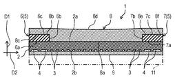
- FIG. 1 is an overall perspective view of a touch sensor according to an embodiment of the present disclosure.
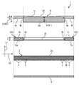
- 2 is a cross-sectional view taken along the line II-II in FIG.
- FIG. 3 is an exploded cross-sectional view showing each component of the touch sensor shown in FIG. 2 in an exploded manner.
- the cover glass is formed so that the thickness thereof is larger than the thickness of the substrate. Furthermore, the cover glass is laminated and disposed on the upper side of the transparent substrate and the decorative portion via an optical pressure-sensitive adhesive having a predetermined thickness (see FIG. 2 and paragraph 0043 of Patent Document 1). Thus, there existed a problem that the whole thickness of a touch sensor will increase with the thickness of each of a cover glass and an optical adhesive. That is, it is difficult to reduce the thickness of the touch sensor disclosed in Patent Document 1.
- the touch sensor of the present disclosure can be thinned.
- FIG. 1 illustrates an entire touch sensor 1 according to an embodiment of the present disclosure.
- the touch sensor 1 is a sensor type input device capable of a touch operation.
- the touch sensor 1 is for an external device (not shown) such as an in-vehicle device such as a car navigation system, a display device of a personal computer, a mobile phone, a portable information terminal, a portable game machine, a copy machine, a ticket vending machine, an automatic teller machine, etc. Used as an input device.
- the touch sensor 1 is provided with a flexible wiring board 10 for electrical connection with the external device.
- a direction from the second surface 2b to the first surface 2a of the substrate unit 2 described later with reference to FIG. 3 is defined as a first direction D1 and a direction orthogonal to the first direction D1.
- the second direction D2 (see the arrows shown in FIGS. 2 and 3) is defined.
- viewing from the first direction will be described as “plan view”.
- the positional relationship of the touch sensor 1 and each component mentioned later is specified mainly based on the 1st direction D1 and the 2nd direction D2. However, such a positional relationship is independent of the actual direction in the touch sensor 1 or the device in which it is incorporated.
- the touch sensor 1 includes a substrate portion 2 having transparency.
- the substrate unit 2 includes, for example, a resin material having optical transparency such as polycarbonate, polyethylene terephthalate, polyethersulfone, PMMA (acrylic), COP (cycloolefin polymer), or glass.
- the substrate part 2 is formed, for example, in a rectangular shape in a plan view, and has a thickness of about 1 to 3 mm. Moreover, the board
- substrate part 2 has the 1st surface 2a and the 2nd surface 2b located in the other side of the 1st surface 2a. In the present embodiment, it is assumed that the first surface 2a is positioned on the side where the user visually recognizes (operates), for example, while the second surface 2b is positioned on the side where the display is arranged. However, it is not limited to such a positional relationship.
- sensor electrodes 3, 3, On the second surface 2b of the substrate portion 2, sensor electrodes 3, 3,.
- the sensor electrodes 3, 3,... are, for example, capacitance type capable of detecting a touch operation by a user's finger (detection target) in contact with a fourth coat surface 8 d in the first hard coat layer 8 described later. It is comprised as a sensor body.
- Each sensor electrode 3 is electrically connected to the external device via routing wirings 4, 4,... Described later and the flexible wiring board 10.
- Each of the sensor electrodes 3, 3,... Has, for example, a mesh structure in which a plurality of conductive thin wires are arranged in a mesh shape.
- the network structure is configured as a conductive layer in which a conductive metal described later is embedded in a plurality of grooves formed on the second surface 2b of the substrate unit 2.
- each sensor electrode 3 is preferably a conductive metal such as silver, copper, aluminum, nickel, molybdenum, or an alloy of copper and nickel, but may be a conductive resin material.
- the line width of each sensor electrode 3 is preferably about 2 ⁇ m, for example. Examples of the method for forming each sensor electrode 3 include sputtering deposition, plating, photolithography, screen printing, CMP polishing (embedding formation), and the like.
- routing wiring 4 On the second surface 2 b of the substrate portion 2, routing wirings 4, 4,... For electrical connection with the external circuit are provided via the flexible wiring board 10.
- the line width of each routing wiring 4 is preferably about 6 ⁇ m, for example.
- Each routing wire 4 has one end portion electrically connected to each sensor electrode 3 and the other end portion electrically connected to the flexible wiring board 10.
- Each lead wiring 4 is made of the same material as that of the sensor electrode 3 and is formed by the same formation method.
- a light source body 11 for irradiating light to the sensor electrodes 3, 3,.
- the light source body 11 is disposed below the substrate unit 2.
- an LCD display, an LED, or the like is suitable as the light source body 11.
- the touch sensor 1 includes a decoration unit 5.
- the decorating unit 5 can conceal the routing wirings 4, 4,... From the viewing side of the touch sensor 1 (see FIGS. 2 and 3).
- the decoration part 5 is formed in a substantially frame shape so as to correspond to the entire periphery of the touch sensor 1 in plan view.
- the decoration unit 5 is made of a resin material containing a color pigment having a black color, for example.
- the decorating part 5 is formed on the first surface 2a of the substrate part 2 by coating or printing. That is, the decorating unit 5 is disposed on the surface of the substrate unit 2 that is located on the viewing side of the touch sensor 1.
- the decorative portion 5 is preferably formed to have a thickness of 10 to 15 ⁇ m, for example.
- the decorative portion 5 has a first decorative layer 6 and a second decorative layer 7.
- the first decorative layer 6 includes a first decorative surface 6a in contact with the first surface 2a of the substrate portion 2.
- the first decorating surface 6a is formed along the second direction D2.
- the first decorative layer 6 includes a second decorative surface 6b connected to the first decorative surface 6a.
- the second decorating surface 6b is formed along the first direction D1.
- the 1st decoration layer 6 contains the 3rd decoration surface 6c connected with the 1st decoration surface 6a via the 2nd decoration surface 6b.
- the 3rd decorating surface 6c is formed so that it may be located in the 1st direction D1 rather than the 1st decorating surface 6a, and may follow the 2nd direction D2.
- the second decorative layer 7 includes a fourth decorative surface 7a in contact with the first surface 2a of the substrate portion 2.
- the fourth decorative surface 7a is formed along the second direction D2.
- the second decorative layer 7 includes a fifth decorative surface 7b that is connected to the fourth decorative surface 7a and faces the second decorative surface 6b.
- the fifth decorative surface 7b is formed along the first direction D1.
- the 2nd decoration layer 7 contains the 6th decoration surface 7c connected with the 4th decoration surface 7a via the 5th decoration surface 7b.
- the sixth decorating surface 7c is formed so as to be positioned in the first direction D1 and along the second direction D2 relative to the fourth decorating surface 7a.
- the touch sensor 1 includes a first hard coat layer 8 having optical transparency. As shown in FIGS. 2 and 3, the first hard coat layer 8 is formed on the first surface 2a of the substrate portion 2 by coating or printing.
- the first hard coat layer 8 is made of a transparent resin material having ultraviolet curing property or heat sensitivity.
- a material for the first hard coat layer 8 for example, acrylate, methacrylate or the like is suitable.
- polyfunctional acrylates and polyfunctional methacrylates such as polyfunctional acrylates and polyfunctional methacrylates are suitable.
- the first hard coat layer 8 preferably has a hardness that is harder than the substrate. Specifically, the hardness of the first hard coat layer 8 is preferably in the range of B to 9H. Specific characteristics of the first hard coat layer 8 will be described later.
- the first hard coat layer 8 includes first to sixth coat surfaces 8a to 8f.
- the first coat surface 8a is formed along the second direction D2.
- the first coat surface 8 a is in contact with the first surface 2 a of the substrate unit 2.
- the second coat surface 8b is connected to the first coat surface 8a.
- the second coat surface 8b is formed along the first direction D1.
- the second coat surface 8b is in contact with the second decorative surface 6b in the second direction D2.
- the third coat surface 8c is connected to the second coat surface 8b.
- the third coat surface 8c is formed along the second direction D2.
- the third coat surface 8c is in contact with the third decorative surface 6c in the first direction D1.
- the fourth coat surface 8d is located in the first direction D1 relative to the first coat surface 8a and the third coat surface 8c.
- the fourth coat surface 8d is formed along the second direction D2.
- the fifth coat surface 8e is connected to the first coat surface 8a.
- the fifth coat surface 8e is formed along the first direction D1.
- the fifth coat surface 8e is in contact with the fifth decorative surface 7b in the second direction D2.
- the sixth coat surface 8f is connected to the fifth coat surface 8e.
- the sixth coat surface 8f is formed along the second direction D2.
- the sixth coated surface 8f is in contact with the sixth decorative surface 7c in the first direction D1.
- the distance between the third coated surface 8c and the fourth coated surface 8d is a dimension A
- the first coated surface 8a and the fourth coated surface 8d is defined as a dimension B, respectively.
- region) between the 2nd decorating surface 6b and the 5th decorating surface 7b be the area (beta).
- an area (second area) positioned in the first direction D1 at least with respect to the area ⁇ is defined as an area ⁇ .
- the first hard coat layer 8 has a distance (dimension A) between the third coated surface 8c and the fourth coated surface 8d in the first direction D1 and the first decorative surface 6a. It is comprised so that it may become smaller than the distance (dimension C) between 3 decorative surfaces 6c.
- the first hard coat layer 8 has a distance (dimension B) in the first direction D1 between the first coat surface 8a and the fourth coat surface 8d so that the first decorative surface 6a and the fourth coat surface 8d
- the distance (dimension A) in the first direction D1 between the third coated surface 8c and the fourth coated surface 8d is the distance (dimension C) in the first direction D1 between the third decorative surface 6c and the third decorated surface 6c.
- the area ⁇ has a portion that is smaller than the distance (the total dimension of the dimension A and the dimension C) added.
- the distance (dimension B1) between the first coated surface 8a and the fourth coated surface 8d is the area ⁇ . Is smaller than the distance (dimension B2) between the first coated surface 8a and the fourth coated surface 8d in the peripheral region.
- At least the first hard coat layer 8 in the area ⁇ is formed so that the surface roughness of the fourth coat surface 8d is 0.05 ⁇ m or more and 1.1 ⁇ m or less.
- polishing and other well-known chemical methods are mentioned, for example.
- the first hard coat layer 8 is preferably configured such that the dimension B is larger than the dimension C.
- the dimension B that is, the thickness of the first hard coat layer 8
- the refractive index of the substrate portion 2 is preferably set to 1.58 to 1.6
- the refractive index of the first hard coat layer 8 is preferably set to 1.51 to 1.52.
- the refractive index difference between the substrate portion 2 and the first hard coat layer 8 becomes 0.1 or less.
- the first hard coat layer 8 for example, when a mixture in which a photopolymerization initiator (alkylphenone photopolymerization initiator) is blended with a polyfunctional acrylate ester or a polyfunctional methacrylic acid ester as a main ingredient is applied. Good. Specifically, the unreacted photopolymerization initiator is 0.43 wt% or less (1.3 wt% to 2.17 wt% at the time of preparation, the degree of polymerization is 80% or more), and the upper and lower film thickness ratio is 0.75 to 1. Within 5 times. In this way, it is possible to suppress vertical warping in the touch sensor 1.
- a photopolymerization initiator alkylphenone photopolymerization initiator
- the touch sensor 1 includes a second hard coat layer 9 having light transparency. Similar to the first hard coat layer 8, the second hard coat layer 9 is made of a transparent resin material having ultraviolet curability or heat sensitivity. The second hard coat layer 9 is formed on the second surface 2 b of the substrate unit 2. Specifically, the second hard coat layer 9 is formed by applying or printing the resin material on the second surface 2b. Similarly to the first hard coat layer 8, the second hard coat layer 9 is configured to have a hardness in the range of B to 9H.
- the second hard coat layer 9 is formed so that the surface roughness is 0.05 ⁇ m or more and 1.1 ⁇ m or less.
- a photopolymerization initiator alkylphenone photopolymerization initiator
- a polyfunctional acrylate ester or polyfunctional methacrylic acid ester as a main ingredient is applied. May be.
- the first hard coat layer 8 faces the first coat surface 8 a in contact with the substrate portion 2 and the second decorative surface 6 b and is connected to the first coat surface 8 a. 2nd coat surface 8b. With the first coat surface 8a and the second coat surface 8b, the first hard coat layer 8 can be disposed along both the substrate portion 2 and the second decorative surface 6b. This eliminates the need for members such as a cover glass and a pressure-sensitive adhesive that cause the overall thickness to increase as in the conventional touch sensor. That is, the touch sensor 1 can reduce the overall thickness. Therefore, according to the embodiment of the present disclosure, the thin touch sensor 1 can be provided.
- the first coated surface 8a is in contact with the first surface 2a of the substrate part 2, the first coated surface 8a can be closely adhered to the first surface 2a. Thereby, the adhesiveness of the board
- the first hard coat layer 8 is configured such that the second coat surface 8b is in contact with the second decorative surface 6b. That is, the second coat surface 8b can be closely adhered to the second decorative surface 6b without any gap. Thereby, the adhesiveness of the 1st decorating layer 6 and the 1st hard-coat layer 8 can be improved.
- the first hard coat layer 8 includes a third coat surface 8c that is connected to the second coat surface 8b and is in contact with the third decorative surface 6c. Thereby, it becomes possible to make the 3rd coating surface 8c closely_contact
- the first hard coat layer 8 includes a fourth coat surface 8d located in the first direction D1 with respect to the first coat surface 8a and the third coat surface 8c.
- the fourth decorative surface 8d can appropriately protect the first decorative layer 6 from the outside of the touch sensor 1 (for example, the viewing side).
- the cover glass and adhesive like a touch sensor of a prior art become unnecessary, compared with the touch sensor of a prior art, it is the 1st decoration layer from the 4th coating surface 8d.
- the number of interfaces up to 6 is reduced. That is, only the interface between the fourth coat surface 8d and the air layer and the interface between the fourth coat surface 8d and the first decorative layer 6 exist at the position where the fourth coat surface 8d is located. Only.
- the distance (dimension A in FIG. 3) in the first direction D1 between the third coated surface 8c and the fourth coated surface 8d is the first decorated surface 6a and the third decorated surface 6c. Is smaller than the distance in the first direction D1 (dimension C in FIG. 3). For this reason, it is possible to appropriately protect the first decorative layer 6 by the fourth coat surface 8d while suppressing the overall thickness of the touch sensor 1.
- the first hard coat layer 8 is connected to the first coat surface 8a and is in contact with the fifth decorative surface 7b, and is connected to the fifth coat surface 8e and is connected to the sixth coat surface 8e.
- a sixth coat surface 8f in contact with the decorative surface 7c is included.
- the hardness of the first hard coat layer 8 is in the range of B to 9H. Thereby, the intensity
- the surface roughness of the fourth coated surface 8d is at least in the area ⁇ located in the first direction D1 than the region (area ⁇ ) between the second decorative surface 6b and the fifth decorative surface 7b.
- the degree is 0.05 ⁇ m or more and 1.1 ⁇ m or less.
- the first hard coat layer 8 has a distance (dimension B) in the first direction D1 between the first coat surface 8a and the fourth coat surface 8d so that the first decorative surface 6a and the fourth coat surface 8d
- the distance (dimension A) in the first direction D1 between the third coated surface 8c and the fourth coated surface 8d is the distance (dimension C) in the first direction D1 between the third decorative surface 6c and the third decorated surface 6c.
- the position corresponding to the region (area ⁇ ) between the second decorative surface 6b and the fifth decorative surface 7b is a portion that is smaller than the distance (the total size of the dimension A and the dimension C) plus (Area ⁇ ). Thereby, the thickness of the touch sensor 1 can be further reduced at least at a position corresponding to the area ⁇ .
- the hardness of the second hard coat layer 9 is in the range of B to 9H. Thereby, the intensity
- the hardness of the second hard coat layer 9 is equal to the hardness of the first hard coat layer 8.
- the form in which the surface roughness of at least the fourth coat surface 8d located in the area ⁇ is 0.05 ⁇ m or more and 1.1 ⁇ m or less is shown. I can't.
- the anti-glare treatment is performed so that the surface roughness of at least the fourth coat surface 8d located in the area ⁇ is greater than 1.1 ⁇ m and less than 4.5 ⁇ m. May be.
- the fourth coated surface 8d positioned at least in the area ⁇ is roughened as compared with the first embodiment, so that the fourth coated surface in which external light is positioned at least in the area ⁇ . It becomes easy to diffuse at 8d. Thereby, the reflection of the first hard coat layer 8 due to external light is suppressed, and the antiglare property of the touch sensor 1 is increased. That is, the visibility of the touch sensor 1 can be improved.
- the surface roughness of the surface located in the direction opposite to the first direction D1 of the second hard coat layer 9 may be greater than 1.1 ⁇ m and not greater than 4.5 ⁇ m.
- a fine uneven structure (so-called moth-eye structure) having a fine uneven shape (not shown) may be added to the fourth coated surface 8d located in at least the area ⁇ shown in the first modification.
- the concavo-convex shape is formed so that the pitch between adjacent convex portions is a pitch smaller than the wavelength of visible light (380 to 780 nm).
- the second hard coat layer 9 may also be provided with a moth-eye structure on the surface located in the direction opposite to the first direction D1.
- substrate part 2 may be comprised as the laminated body which piled up the some board
- substrate part 2 may be comprised as a composite laminated body which piled up the single or several board
- substrate part 2 consists of a composite laminated body, it comprises so that the 1st surface 2a may become the surface of a composite laminated body, and the 2nd surface 2b may become the back surface of a composite laminated body. do it.
- the decoration part 5 is formed in a substantially frame shape so as to correspond to the entire periphery of the touch sensor 1, but is not limited to this form, and various shapes can be adopted.
- positioned the decoration part 5 only in the position corresponding to the both sides which mutually oppose in the periphery of the touch sensor 1 namely, the decoration part 5 is the 1st decoration layer 6 and the 2nd decoration layer 7. It is good also as a form which has only.
- the second hard coat layer 9 has a configuration in which the hardness is in the range of B to 9H, that is, the second hard coat layer 9 is the first hard coat layer 8.
- the second hard coat layer 9 may be configured such that its hardness is greater than the hardness of the first hard coat layer 8. If comprised in this way, the 2nd hard-coat layer 9 can be formed thinly.
- each sensor electrode 3 and each routing wiring 4 were comprised as a conductive layer which embed
- the sensor electrodes 3 and the routing wires 4 may be stacked on the second surface 2 b of the substrate portion 2 without providing a plurality of groove portions.
- the material of each sensor electrode 3 and each routing wiring 4 is not limited to the above conductive metal or conductive resin material, and for example, a transparent material (transparent conductive film) having optical transparency such as indium tin oxide and tin oxide. May be used.
- each sensor electrode 3 and each routing wiring 4 is formed on the second surface 2b side of the substrate unit 2, but the present invention is not limited to this. That is, each sensor electrode 3 and each routing wiring 4 may be formed on the first surface 2 a side of the substrate portion 2.
- the touch sensor 1 of the present disclosure described above is formed on the substrate surface 2 including the first surface 2a and the second surface 2b located on the opposite side of the first surface 2a, and the first surface 2a of the substrate portion 2.
- the 1st hard-coat layer 8 which has a light transmittance, and the 1st decoration which was formed in the 1st surface 2a of the board
- the 1st decoration layer 6 contains the 1st decoration surface 6a which contact
- the first hard coat layer 8 is a second coat surface facing the first coat surface 8a in contact with the first surface 2a of the substrate portion 2 and the second decorative surface 6b and connected to the first coat surface 8a. 8b.
- the second coat surface 8b is in contact with the second decorative surface 6b.
- the direction from the second surface 2b to the first surface 2a is defined as a first direction D1
- the first decorative layer 6 is positioned in the first direction D1 with respect to the substrate portion 2
- the first decorative layer 6 further includes a third decorative surface 6c connected to the first decorative surface 6a via the second decorative surface 6b
- the first hard coat layer 8 includes the substrate portion 2.
- the first hard coat layer 8 is further connected to the second coat surface 8b and further includes a third coat surface 8c in contact with the third decorative surface 6c. Also good.
- the first hard coat layer 8 further includes a fourth coat surface 8d positioned in the first direction D1 with respect to the first coat surface 8a and the third coat surface 8c.
- the distance (dimension A) in the first direction D1 between the coat surface 8c and the fourth coat surface 8d is the first direction between the first decorative surface 6a and the third decorative surface 6c. It is preferable that the distance is smaller than the distance (dimension C) in D1.
- the decorative portion 5 further includes a second decorative layer 7 formed on the substrate portion 2, and the second decorative layer 7 is in contact with the first surface 2 a of the substrate portion 2.
- the sixth decorative surface 7c connected to the fifth decorative surface 7b.
- the first hard coat layer 8 is connected to the first coated surface 8a, and the fifth decorative surface 7b.
- a fifth coated surface 8e that contacts the fifth coated surface 8e and a sixth coated surface 8f that contacts the sixth decorative surface 7c.
- the hardness of the first hard coat layer 8 is preferably in the range of B to 9H.
- the surface roughness of the fourth coated surface 8d is preferably 0.05 ⁇ m or more and 1.1 ⁇ m or less.
- the surface roughness of the fourth coated surface 8d may be greater than 1.1 ⁇ m and 4.5 ⁇ m or less.
- At least part of the fourth coated surface 8d is such that the distance (dimension B1) in the first direction D1 between the first coated surface 8a and the fourth coated surface 8d is the first decorative surface.
- the distance (dimension C) in the first direction D1 between 6a and the third decorative surface 6c in the first direction D1 between the third coated surface 8c and the fourth coated surface 8d ( It is preferable that the distance is smaller than the distance (dimension B2) including dimension A).
- the touch sensor 1 further includes a second hard coat layer 9 formed on the second surface 2b of the substrate unit 2, and the hardness of the second hard coat layer 9 is preferably in the range of B to 9H. .
- the hardness of the second hard coat layer 9 is preferably equal to the hardness of the first hard coat layer 8.
- the first decorative layer 6 is made of a resin material containing a color pigment.
- the first hard coat layer 8 is preferably made of a transparent resin material.
- the touch sensor of the present disclosure can be industrially used as a sensor-type input device capable of touch operation.
Landscapes
- Engineering & Computer Science (AREA)
- General Engineering & Computer Science (AREA)
- Theoretical Computer Science (AREA)
- Human Computer Interaction (AREA)
- Physics & Mathematics (AREA)
- General Physics & Mathematics (AREA)
- Position Input By Displaying (AREA)
- Laminated Bodies (AREA)
Abstract
本開示のタッチセンサは、第1面と、前記第1面の反対側に位置する第2面と、を含む基板部と、前記基板部の前記第1面に形成され、光透過性を有する第1のハードコート層と、前記基板部の前記第1面に形成され、前記第1のハードコート層より光透過性が低く、かつ着色された第1の加飾層を有する加飾部と、を備え、前記第1の加飾層は、前記基板部の前記第1面と接する第1の加飾面と、前記第1の加飾面と繋がる第2の加飾面と、を含み、前記第1のハードコート層は、前記基板部の前記第1面と接する第1のコート面と、前記第2の加飾面と向かい合い、前記第1のコート面と繋がる第2のコート面と、を含む。
Description
本開示はタッチセンサに関する。
従来から、タッチセンサに関して、例えば特許文献1が知られている。
特許文献1には、透明基材と、少なくとも透明基材の表面に形成されたセンサ電極および外周配線と、透明基材の表面に位置する外周配線をその上側から覆うように透明基材の表面に形成された加飾部と、強化ガラスからなるカバーガラスと、を備えたタッチセンサが開示されている。
本開示の一態様に係るタッチセンサは、第1面と、前記第1面の反対側に位置する第2面と、を含む基板部と、前記基板部の前記第1面に形成され、光透過性を有する第1のハードコート層と、前記基板部の前記第1面に形成され、前記第1のハードコート層より光透過性が低く、かつ着色された第1の加飾層を有する加飾部と、を備え、前記第1の加飾層は、前記基板部の前記第1面と接する第1の加飾面と、前記第1の加飾面と繋がる第2の加飾面と、を含み、前記第1のハードコート層は、前記基板部の前記第1面と接する第1のコート面と、前記第2の加飾面と向かい合い、前記第1のコート面と繋がる第2のコート面と、を含む。
本開示のタッチセンサによると、薄型のタッチセンサを提供できる。
上述した従来のタッチセンサでは、カバーガラスの厚みが基板の厚みよりも大きくなるように形成されている。さらに、カバーガラスは、所定の厚みを有する光学用粘着剤を介して透明基板および加飾部の上側に積層配置されている(特許文献1の図2および段落0043を参照)。このように、カバーガラスおよび光学用粘着剤の各々の厚みにより、タッチセンサの全体的な厚みが増大してしまうという問題があった。すなわち、特許文献1のタッチセンサでは、薄型化が困難となっていた。本開示のタッチセンサは、薄型化を実現できる。
(実施の形態)
以下、本開示の実施形態について図面を参照しながら詳細に説明する。以下の実施形態の説明は、本質的に例示に過ぎず、本開示、その適用物或いはその用途を制限することを意図しない。
以下、本開示の実施形態について図面を参照しながら詳細に説明する。以下の実施形態の説明は、本質的に例示に過ぎず、本開示、その適用物或いはその用途を制限することを意図しない。
図1は、本開示の実施形態に係るタッチセンサ1の全体を示している。このタッチセンサ1は、タッチ操作が可能なセンサ型入力装置である。タッチセンサ1は、図示しない外部装置(例えばカーナビゲーション等の車載装置、パーソナルコンピュータのディスプレイ機器、携帯電話、携帯情報端末、携帯型ゲーム機、コピー機、券売機、現金自動預け払い機など)に対する入力装置として用いられる。図1に示すように、タッチセンサ1には、上記外部装置と電気的に接続するためのフレキシブル配線板10が設けられている。
なお、以下の説明では、図3を参照しながら後述する基板部2の第2面2bから第1面2aへと向かう方向を第1の方向D1としかつ第1の方向D1に直交する方向を第2の方向D2(図2および図3に示した矢印を参照)として定めるものとする。以下では、第1の方向から見ることを「平面視」として説明する。そして、主に第1の方向D1および第2の方向D2に基づいてタッチセンサ1および後述する各構成要素の位置関係を特定している。しかしながら、このような位置関係は、タッチセンサ1またはそれが組み込まれた機器における実際の方向とは無関係である。
[基板部2の構成]
図2および図3に示すように、タッチセンサ1は、透明性を有する基板部2を備えている。基板部2は、例えばポリカーボネート、ポリエチレンテレフタレート、ポリエーテルサルホン、PMMA(アクリル)、COP(シクロオレフィンポリマー)等のような光透過性を有する樹脂材または、ガラスを含む。
図2および図3に示すように、タッチセンサ1は、透明性を有する基板部2を備えている。基板部2は、例えばポリカーボネート、ポリエチレンテレフタレート、ポリエーテルサルホン、PMMA(アクリル)、COP(シクロオレフィンポリマー)等のような光透過性を有する樹脂材または、ガラスを含む。
基板部2は、平面視で、例えば長方形に形成されていて、約1~3mmの厚みを有している。また、基板部2は、第1面2aと、第1面2aの反対側に位置する第2面2bとを有している。なお、本実施形態では、第1面2aが、例えば使用者が視認する(操作する)側に位置している一方、第2面2bが、ディスプレイが配置される側に位置しているものとしているが、このような位置関係に限定されない。
[センサ電極3の構成]
基板部2の第2面2bには、センサ電極3,3,…が設けられている。センサ電極3,3,…は、例えば、後述する第1のハードコート層8における第4のコート面8dに接触した使用者の手指(検知対象物)によるタッチ操作を検知可能な静電容量式のセンサ体として構成されている。各センサ電極3は、後述する引き回し配線4,4,…および上記フレキシブル配線板10を介して上記外部機器と電気的に接続されている。
基板部2の第2面2bには、センサ電極3,3,…が設けられている。センサ電極3,3,…は、例えば、後述する第1のハードコート層8における第4のコート面8dに接触した使用者の手指(検知対象物)によるタッチ操作を検知可能な静電容量式のセンサ体として構成されている。各センサ電極3は、後述する引き回し配線4,4,…および上記フレキシブル配線板10を介して上記外部機器と電気的に接続されている。
センサ電極3,3,…のそれぞれは、例えば、導電性を有する複数の細線をメッシュ状に配置した網目構造により構成されている。この網目構造は、基板部2の第2面2bに形成された複数の溝部内に後述する導電金属が埋設された導電層として構成されている。
各センサ電極3の材質としては、例えば銀、銅、アルミニウム、ニッケル、モリブデン、または銅とニッケルとの合金などの導電金属が望ましいが、導電樹脂材などであってもよい。各センサ電極3の線幅は、例えば約2μmが好適である。また、各センサ電極3の形成方法としては、スパッタ蒸着法、メッキ処理、フォトリソグラフィー法、スクリーン印刷法、CMP研磨(埋設形成)等が挙げられる。
[引き回し配線4の構成]
基板部2の第2面2bには、フレキシブル配線板10を介して上記外部回路と電気的に接続するための引き回し配線4,4,…が設けられている。各引き回し配線4の線幅は、例えば約6μmが好適である。各引き回し配線4は、一端部が各センサ電極3と電気的に接続されかつ他端部がフレキシブル配線板10と電気的に接続されている。なお、各引き回し配線4は、センサ電極3と同様の材料からなりかつ同様の形成方法により形成される。
基板部2の第2面2bには、フレキシブル配線板10を介して上記外部回路と電気的に接続するための引き回し配線4,4,…が設けられている。各引き回し配線4の線幅は、例えば約6μmが好適である。各引き回し配線4は、一端部が各センサ電極3と電気的に接続されかつ他端部がフレキシブル配線板10と電気的に接続されている。なお、各引き回し配線4は、センサ電極3と同様の材料からなりかつ同様の形成方法により形成される。
図2に示すように、基板部2の下方には、センサ電極3,3,…に対して光を照射するための光源体11が設けられている。光源体11は、基板部2の下方に配設されている。光源体11としては、LCDディスプレイ、LEDなどが適している。
[加飾部5の構成]
図1に示すように、タッチセンサ1は、加飾部5を備えている。加飾部5は、引き回し配線4,4,…をタッチセンサ1の視認側から隠蔽することができる(図2および図3参照)。この実施形態において、加飾部5は、平面視でタッチセンサ1の周縁全体に対応するように略額縁状に形成されている。
図1に示すように、タッチセンサ1は、加飾部5を備えている。加飾部5は、引き回し配線4,4,…をタッチセンサ1の視認側から隠蔽することができる(図2および図3参照)。この実施形態において、加飾部5は、平面視でタッチセンサ1の周縁全体に対応するように略額縁状に形成されている。
加飾部5は、例えば黒色系の色となる着色顔料を含む樹脂材からなる。加飾部5は、塗布または印刷等により基板部2の第1面2aに形成されている。すなわち、加飾部5は、基板部2においてタッチセンサ1の視認側に位置する面に配置されている。なお、加飾部5は、その厚みが例えば10~15μmとなるように形成されているのが好ましい。
図2および図3に示すように、加飾部5は、第1の加飾層6および第2の加飾層7を有している。
第1の加飾層6は、基板部2の第1面2aと接する第1の加飾面6aを含んでいる。第1の加飾面6aは、第2の方向D2に沿うように形成されている。
第1の加飾層6は、第1の加飾面6aと繋がる第2の加飾面6bを含んでいる。第2の加飾面6bは、第1の方向D1に沿うように形成されている。
第1の加飾層6は、第2の加飾面6bを介して第1の加飾面6aと繋がる第3の加飾面6cを含んでいる。第3の加飾面6cは、第1の加飾面6aよりも第1の方向D1に位置しかつ第2の方向D2に沿うように形成されている。
第2の加飾層7は、基板部2の第1面2aと接する第4の加飾面7aを含んでいる。第4の加飾面7aは、第2の方向D2に沿うように形成されている。
第2の加飾層7は、第4の加飾面7aと繋がり、第2の加飾面6bと向かい合う第5の加飾面7bを含んでいる。第5の加飾面7bは、第1の方向D1に沿うように形成されている。
第2の加飾層7は、第5の加飾面7bを介して第4の加飾面7aと繋がる第6の加飾面7cを含んでいる。第6の加飾面7cは、第4の加飾面7aよりも第1の方向D1に位置しかつ第2の方向D2に沿うように形成されている。
[第1のハードコート層8の構成]
図1に示すように、タッチセンサ1は、光透過性を有する第1のハードコート層8を備えている。図2および図3に示すように、第1のハードコート層8は、塗布または印刷により基板部2の第1面2aに形成されている。
図1に示すように、タッチセンサ1は、光透過性を有する第1のハードコート層8を備えている。図2および図3に示すように、第1のハードコート層8は、塗布または印刷により基板部2の第1面2aに形成されている。
第1のハードコート層8は、紫外線硬化性または感熱性を有する透明な樹脂材からなる。具体的に、第1のハードコート層8の材料としては、例えばアクリレートやメタクリレート等が適している。特に、多官能アクリレートや多官能メタクリレートなど、多官能アクリル酸エステルや多官能メタアクリル酸エステルが適している。第1のハードコート層8は、基板よりも固くなるような硬度を有しているのが好ましい。具体的に、第1のハードコート層8の硬度は、B~9Hの範囲内であることが好ましい。第1のハードコート層8の具体的な特性については後述する。
図2および図3に示すように、第1のハードコート層8は、第1~第6のコート面8a~8fを含んでいる。
第1のコート面8aは、第2の方向D2に沿うように形成されている。第1のコート面8aは、基板部2の第1面2aと接している。
第2のコート面8bは、第1のコート面8aと繋がっている。第2のコート面8bは、第1の方向D1に沿うように形成されている。第2のコート面8bは、第2の方向D2で第2の加飾面6bと向かい合った状態で接している。
第3のコート面8cは、第2のコート面8bと繋がっている。第3のコート面8cは、第2の方向D2に沿うように形成されている。第3のコート面8cは、第1の方向D1で第3の加飾面6cと向かい合った状態で接している。
第4のコート面8dは、第1のコート面8aおよび第3のコート面8cよりも第1の方向D1に位置している。第4のコート面8dは、第2の方向D2に沿うように形成されている。
第5のコート面8eは、第1のコート面8aと繋がっている。第5のコート面8eは、第1の方向D1に沿うように形成されている。第5のコート面8eは、第2の方向D2で第5の加飾面7bと向かい合った状態で接している。
第6のコート面8fは、第5のコート面8eと繋がっている。第6のコート面8fは、第2の方向D2に沿うように形成されている。第6のコート面8fは、第1の方向D1で第6の加飾面7cと向かい合った状態で接している。
ここで、図3に示すように、第1の方向D1において、第3のコート面8cと第4のコート面8dとの間の距離を寸法Aとし、第1のコート面8aと第4のコート面8dとの間の距離を寸法Bとし、第1の加飾面6aと第3の加飾面6cとの間の距離を寸法Cとする。また、第2の加飾面6bと第5の加飾面7bとの間の領域(第1の領域)をエリアβとする。さらに、少なくともエリアβに対して第1の方向D1に位置する領域(第2の領域)をエリアαとする。
そして、第1のハードコート層8は、第1の方向D1において、第3のコート面8cと第4のコート面8dとの間の距離(寸法A)が第1の加飾面6aと第3の加飾面6cとの間の距離(寸法C)よりも小さくなるように構成されている。
また、第1のハードコート層8は、第1のコート面8aと第4のコート面8dとの間の第1の方向D1における距離(寸法B)が、第1の加飾面6aと第3の加飾面6cとの間の第1の方向D1における距離(寸法C)に第3のコート面8cと第4のコート面8dとの間の第1の方向D1における距離(寸法A)を加えた距離(寸法Aと寸法Cとの合計寸法)よりも小さくなる部位を、エリアαに有している。
つまり、図3に示すように、エリアβとD1方向に重なる領域(エリアα)においては、第1のコート面8aと第4のコート面8dとの間の距離(寸法B1)は、エリアαの周縁領域における第1のコート面8aと第4のコート面8dとの間の距離(寸法B2)より小さい。
[第1のハードコート層8の具体的特性]
少なくともエリアαの第1のハードコート層8は、第4のコート面8dの表面粗度が0.05μm以上1.1μm以下となるように形成されているのが好ましい。なお、このような表面粗度の形成方法としては、例えば研磨やその他公知の化学的方法が挙げられる。
少なくともエリアαの第1のハードコート層8は、第4のコート面8dの表面粗度が0.05μm以上1.1μm以下となるように形成されているのが好ましい。なお、このような表面粗度の形成方法としては、例えば研磨やその他公知の化学的方法が挙げられる。
また、第1のハードコート層8は、寸法Bが寸法Cよりも大きくなるように構成されているのが好ましい。具体的に、寸法B(すなわち、第1のハードコート層8の厚み)が18μm以上32μm以下であるのが好ましい。そして、基板部2の屈折率を1.58~1.6とし、かつ第1のハードコート層8の屈折率を1.51~1.52となるように設定するのが好ましい。これにより、基板部2と第1のハードコート層8との屈折率差が0.1以下となる。その結果、タッチセンサ1の光透過性が確保されるとともに、タッチセンサ1の上面に虹模様が現れないようにすることが可能となる。
さらに、第1のハードコート層8として、たとえば、多官能アクリル酸エステルや多官能メタアクリル酸エステルを主剤として、光重合開始剤(アルキルフェノン系光重合開始剤)を配合させた混合物を適用するとよい。具体的に、未反応の光重合開始剤を0.43wt%以下(調合時1.3wt%~2.17wt%、重合度80%以上)とし、かつ上下膜厚比を0.75~1.5倍以内とする。このようにすれば、タッチセンサ1における上下方向の反りを抑えることが可能となる。
[第2のハードコート層9]
タッチセンサ1は、光透過性を有する第2のハードコート層9を備えている。第2のハードコート層9は、第1のハードコート層8と同様に、紫外線硬化性または感熱性を有する透明な樹脂材からなる。第2のハードコート層9は、基板部2の第2面2bに形成されている。具体的に、第2のハードコート層9は、上記樹脂材を第2面2b上に塗布または印刷することにより形成されている。また、第2のハードコート層9は、第1のハードコート層8と同様に、その硬度がB~9Hの範囲内となるように構成されている。
タッチセンサ1は、光透過性を有する第2のハードコート層9を備えている。第2のハードコート層9は、第1のハードコート層8と同様に、紫外線硬化性または感熱性を有する透明な樹脂材からなる。第2のハードコート層9は、基板部2の第2面2bに形成されている。具体的に、第2のハードコート層9は、上記樹脂材を第2面2b上に塗布または印刷することにより形成されている。また、第2のハードコート層9は、第1のハードコート層8と同様に、その硬度がB~9Hの範囲内となるように構成されている。
本実施形態において、第2のハードコート層9は、第1のハードコート層8と同様に、表面粗度が0.05μm以上1.1μm以下となるように形成されている。また、第2のハードコート層9として、たとえば、多官能アクリル酸エステルや多官能メタアクリル酸エステルを主剤として、光重合開始剤(アルキルフェノン系光重合開始剤)を配合させた混合物を適用してもよい。
[実施形態の作用効果]
以上のように、タッチセンサ1において、第1のハードコート層8は、基板部2と接する第1のコート面8aと、第2の加飾面6bと向かい合いかつ第1のコート面8aと繋がる第2のコート面8bと、を含んでいる。第1のコート面8aおよび第2のコート面8bにより、第1のハードコート層8を、基板部2および第2の加飾面6bの双方に沿うように配置することが可能となる。これにより、従来技術のタッチセンサのように全体的な厚みが増大する原因となっていたカバーガラスおよび粘着剤といった部材が不要となる。すなわち、タッチセンサ1では、全体的な厚みを薄くすることが可能となる。したがって、本開示の実施形態によれば、薄型のタッチセンサ1を提供することができる。
以上のように、タッチセンサ1において、第1のハードコート層8は、基板部2と接する第1のコート面8aと、第2の加飾面6bと向かい合いかつ第1のコート面8aと繋がる第2のコート面8bと、を含んでいる。第1のコート面8aおよび第2のコート面8bにより、第1のハードコート層8を、基板部2および第2の加飾面6bの双方に沿うように配置することが可能となる。これにより、従来技術のタッチセンサのように全体的な厚みが増大する原因となっていたカバーガラスおよび粘着剤といった部材が不要となる。すなわち、タッチセンサ1では、全体的な厚みを薄くすることが可能となる。したがって、本開示の実施形態によれば、薄型のタッチセンサ1を提供することができる。
さらに、第1のコート面8aが基板部2の第1面2aと接していることから、第1のコート面8aを、第1面2aに対してすき間なく密着させることが可能となる。これにより、基板部2と第1のハードコート層8との密着性を高めることができる。
また、第1のハードコート層8は、第2のコート面8bが第2の加飾面6bと接するように構成されている。すなわち、第2のコート面8bを、第2の加飾面6bに対してすき間なく密着させることが可能となる。これにより、第1の加飾層6と第1のハードコート層8との密着性を高めることができる。
また、第1のハードコート層8は、第2のコート面8bと繋がりかつ第3の加飾面6cと接する第3のコート面8cを含んでいる。これにより、第3のコート面8cを、第3の加飾面6cに対してすき間なく密着させることが可能となる。すなわち、第1の加飾層6と第1のハードコート層8との密着性をより一層高めることができる。
また、第1のハードコート層8は、第1のコート面8aおよび第3のコート面8cよりも第1の方向D1に位置する第4のコート面8dを含んでいる。第4のコート面8dにより、タッチセンサ1の外部(例えば視認側)から第1の加飾層6を適切に保護することができる。そして、タッチセンサ1では、従来技術のタッチセンサのようなカバーガラスおよび粘着剤が不要となることから、従来技術のタッチセンサと比較して、第4のコート面8dから第1の加飾層6までの界面数が削減される。すなわち、第4のコート面8dが位置する箇所では、第4のコート面8dと空気層との界面および第4のコート面8dと第1の加飾層6との界面だけが存在しているに過ぎない。このため、第1の加飾層6が位置する箇所で外光による乱反射を抑制することが可能となり、タッチセンサ1の外部(例えば視認側)から見てぼやけてしまうといった現象(白っぽく見えてしまう現象)を抑えることができる。さらに、第3のコート面8cと第4のコート面8dとの間の第1の方向D1における距離(図3の寸法A)は、第1の加飾面6aと第3の加飾面6cとの間の第1の方向D1における距離(図3の寸法C)よりも小さい。このため、タッチセンサ1の全体的な厚みを抑えつつ、第4のコート面8dにより第1の加飾層6を適切に保護することができる。
また、第1のハードコート層8は、第1のコート面8aと繋がりかつ第5の加飾面7bと接する第5のコート面8eと、第5のコート面8eと繋がりかつ第6の加飾面7cと接する第6のコート面8fとを含んでいる。これにより、第5のコート面8eを第5の加飾面7bに対してすき間なく密着させ、かつ、第6のコート面8fを第6の加飾面7cに対してすき間なく密着させることが可能となる。したがって、第5のコート面8eおよび第6のコート面8fにより、第2の加飾層7と第1のハードコート層8との密着性を高めることができる。
また、第1のハードコート層8の硬度はB~9Hの範囲内である。これにより、例えばタッチセンサ1の視認側の強度を向上させることができる。
また、少なくとも第2の加飾面6bと第5の加飾面7bとの間の領域(エリアβ)よりも第1の方向D1に位置するエリアαにおいて、第4のコート面8dの表面粗度が、0.05μm以上1.1μm以下となっている。これにより、少なくともエリアαに位置する第4のコート面8dの艶やかさを保つことができるとともに、外光による第1のハードコート層8の映り込みを適切に防止することができる。
また、第1のハードコート層8は、第1のコート面8aと第4のコート面8dとの間の第1の方向D1における距離(寸法B)が、第1の加飾面6aと第3の加飾面6cとの間の第1の方向D1における距離(寸法C)に第3のコート面8cと第4のコート面8dとの間の第1の方向D1における距離(寸法A)を加えた距離(寸法Aと寸法Cとの合計寸法)よりも小さくなる部位を、第2の加飾面6bと第5の加飾面7bとの間の領域(エリアβ)に対応する位置(エリアα)に有している。これにより、少なくともエリアαに対応する位置において、タッチセンサ1の厚みをより一層薄くすることができる。
また、第2のハードコート層9の硬度はB~9Hの範囲内である。これにより、例えばタッチセンサ1における視認側の反対側の強度を向上させることができる。
また、本実施形態では、第2のハードコート層9の硬度が第1のハードコート層8の硬度と等しくなっている。これにより、タッチセンサ1の視認側およびその反対側における両側の強度を均一化することができる。
[実施形態の変形例1]
上記実施形態の第1のハードコート層8では、少なくともエリアαに位置する第4のコート面8dの表面粗度が0.05μm以上1.1μm以下となる形態を示したが、この形態に限られない。例えば、変形例1として、防眩処理(アンチグレア処理)を施すことにより、少なくともエリアαに位置する第4のコート面8dの表面粗度が1.1μmよりも大きく4.5μm以下となるようにしてもよい。
上記実施形態の第1のハードコート層8では、少なくともエリアαに位置する第4のコート面8dの表面粗度が0.05μm以上1.1μm以下となる形態を示したが、この形態に限られない。例えば、変形例1として、防眩処理(アンチグレア処理)を施すことにより、少なくともエリアαに位置する第4のコート面8dの表面粗度が1.1μmよりも大きく4.5μm以下となるようにしてもよい。
変形例1では、上記第1実施形態と比較して、少なくともエリアαに位置する第4のコート面8dが粗面化されることから、外光が少なくともエリアαに位置する第4のコート面8dで拡散しやすくなる。これにより、外光による第1のハードコート層8の映り込みが抑制されて、タッチセンサ1の防眩性が高まる。すなわち、タッチセンサ1の視認性を向上させることができる。なお、第2のハードコート層9についても、第1の方向D1と反対方向に位置する面の表面粗度が1.1μmよりも大きく4.5μm以下となるようにしてもよい。
[実施形態の変形例2]
また、図示しない微細な凹凸形状を有する微細凹凸構造(いわゆるモスアイ構造)を、上記変形例1に示した少なくともエリアαに位置する第4のコート面8dに付加してもよい。具体的に、上記凹凸形状を、隣接する凸部同士の頂点間が可視光の波長(380~780nm)よりも小さいピッチとなるように形成する。これにより、可視光波長域の光に対して優れた反射防止効果をタッチセンサ1に付与することができる。なお、第2のハードコート層9についても、第1の方向D1と反対方向に位置する面にモスアイ構造を付与してもよい。
また、図示しない微細な凹凸形状を有する微細凹凸構造(いわゆるモスアイ構造)を、上記変形例1に示した少なくともエリアαに位置する第4のコート面8dに付加してもよい。具体的に、上記凹凸形状を、隣接する凸部同士の頂点間が可視光の波長(380~780nm)よりも小さいピッチとなるように形成する。これにより、可視光波長域の光に対して優れた反射防止効果をタッチセンサ1に付与することができる。なお、第2のハードコート層9についても、第1の方向D1と反対方向に位置する面にモスアイ構造を付与してもよい。
[その他の実施形態]
上記実施形態では、平板状の基板部2を用いた形態を示したが、この形態に限られない。例えば、筐体状に形成された基板部2を適用してもよい。
上記実施形態では、平板状の基板部2を用いた形態を示したが、この形態に限られない。例えば、筐体状に形成された基板部2を適用してもよい。
また、上記実施形態では、基板部2として、一枚の基板部材からなる形態を示したが、この形態に限られない。すなわち、基板部2は、複数の基板部材を重ね合わせた積層体として構成されていてもよい。あるいは、基板部2は、単数または複数の基板部材とフィルム材とを重ね合わせた複合的な積層体として構成されていてもよい。なお、基板部2が複合的な積層体からなる場合には、第1面2aが複合的な積層体の表面となる一方、第2面2bが複合的な積層体の裏面となるように構成すればよい。
また、上記実施形態では、加飾部5を、タッチセンサ1の周縁全体に対応するように略額縁状に形成した形態を示したが、この形態に限られず、種々の形状を採りうる。例えば、加飾部5を、タッチセンサ1の周縁において互いに対向する両辺に対応する位置にのみ配置した形態(すなわち、加飾部5が第1の加飾層6および第2の加飾層7のみを有する形態)としてもよい。あるいは、加飾部5を、タッチセンサ1における周縁の一辺にのみ配置した形態(すなわち、加飾部5が第1の加飾層6および第2の加飾層7のいずれか一方のみを有する形態)としてもよい。
また、上記実施形態では、第2のハードコート層9の硬度がB~9Hの範囲内となるように構成されている形態、すなわち、第2のハードコート層9が第1のハードコート層8の硬度と同じ硬度を有する形態を示したが、この形態に限られない。例えば、第2のハードコート層9は、その硬度が第1のハードコート層8の硬度よりも大きくなるように構成されていてもよい。このように構成すれば、第2のハードコート層9を薄く形成することができる。
また、上記実施形態では、各センサ電極3および各引き回し配線4を、基板部2の第2面2bにおける複数の溝部内に導電金属を埋設した導電層として構成したが、この形態に限られない。すなわち、複数の溝部を設けずに、各センサ電極3および各引き回し配線4を基板部2の第2面2b上に積層配置してもよい。この場合には、各センサ電極3および各引き回し配線4の材質として、上記導電金属や導電樹脂材に限られず、例えば酸化インジウム錫や酸化錫等の光透過性を有する透明材(透明導電膜)を用いてもよい。
また、上記実施形態では、各センサ電極3および各引き回し配線4を基板部2の第2面2b側に形成した形態を示したが、この形態に限られない。すなわち、各センサ電極3および各引き回し配線4を、基板部2の第1面2a側に形成してもよい。
以上、本開示についての実施形態を説明したが、本開示は上述の実施形態のみに限定されず、本開示の範囲内で種々の変更が可能である。
(まとめ)
上述した本開示のタッチセンサ1は、第1面2aと、第1面2aの反対側に位置する第2面2bと、を含む基板部2と、基板部2の第1面2aに形成され、光透過性を有する第1のハードコート層8と、基板部2の第1面2aに形成され、第1のハードコート層8より光透過性が低く、かつ着色された第1の加飾層6を有する加飾部5と、を備える。第1の加飾層6は、基板部2の第1面2aと接する第1の加飾面6aと、第1の加飾面6aと繋がる第2の加飾面6bと、を含む。第1のハードコート層8は、基板部2の第1面2aと接する第1のコート面8aと、第2の加飾面6bと向かい合い、第1のコート面8aと繋がる第2のコート面8bと、を含む。
上述した本開示のタッチセンサ1は、第1面2aと、第1面2aの反対側に位置する第2面2bと、を含む基板部2と、基板部2の第1面2aに形成され、光透過性を有する第1のハードコート層8と、基板部2の第1面2aに形成され、第1のハードコート層8より光透過性が低く、かつ着色された第1の加飾層6を有する加飾部5と、を備える。第1の加飾層6は、基板部2の第1面2aと接する第1の加飾面6aと、第1の加飾面6aと繋がる第2の加飾面6bと、を含む。第1のハードコート層8は、基板部2の第1面2aと接する第1のコート面8aと、第2の加飾面6bと向かい合い、第1のコート面8aと繋がる第2のコート面8bと、を含む。
タッチセンサ1において、第2のコート面8bは、第2の加飾面6bに接していると、好ましい。
タッチセンサ1において、第2面2bから第1面2aに向かう方向を第1の方向D1とし、第1の加飾層6は、基板部2に対して第1の方向D1に位置し、第1の加飾層6は、第2の加飾面6bを介して第1の加飾面6aと繋がる第3の加飾面6cをさらに含み、第1のハードコート層8は、基板部2に対して第1の方向D1に位置し、第1のハードコート層8は、第2のコート面8bと繋がり、第3の加飾面6cと接する第3のコート面8cをさらに含んでいてもよい。
タッチセンサ1において、第1のハードコート層8は、第1のコート面8aおよび第3のコート面8cよりも第1の方向D1に位置する第4のコート面8dをさらに含み、第3のコート面8cと第4のコート面8dとの間の第1の方向D1における距離(寸法A)は、第1の加飾面6aと第3の加飾面6cとの間の第1の方向D1における距離(寸法C)よりも小さくすると、好ましい。
タッチセンサ1において、加飾部5は、基板部2に形成された第2の加飾層7をさらに有し、第2の加飾層7は、基板部2の第1面2aと接する第4の加飾面7aと、第4の加飾面7aと繋がり、第2の加飾面6bと向かい合う第5の加飾面7bと、第4の加飾面7aよりも第1の方向D1に位置し、第5の加飾面7bと繋がる第6の加飾面7cと、を含み、第1のハードコート層8は、第1のコート面8aと繋がり、第5の加飾面7bと接する第5のコート面8eと、第5のコート面8eと繋がり、第6の加飾面7cと接する第6のコート面8fと、をさらに含んでいてもよい。
タッチセンサ1において、第1のハードコート層8の硬度は、B~9Hの範囲内であると、好ましい。
タッチセンサ1において、第2の加飾面6bと第5の加飾面7bとの間の第1の領域(エリアβ)に対して第1の方向D1に位置する第2の領域(エリアα)における第4のコート面8dの表面粗度が、0.05μm以上1.1μm以下であると、好ましい。
タッチセンサ1において、第2の加飾面6bと第5の加飾面7bとの間の第1の領域(エリアβ)に対して第1の方向D1に位置する第2の領域(エリアα)における第4のコート面8dの表面粗度が、1.1μmよりも大きく4.5μm以下であってもよい。
タッチセンサ1において、第2の加飾面6bと第5の加飾面7bとの間の第1の領域(エリアβ)に対して第1の方向D1に位置する第2の領域(エリアα)における第4のコート面8dは、モスアイ構造となっていていると、好ましい。
タッチセンサ1において、第2の加飾面6bと第5の加飾面7bとの間の第1の領域(エリアβ)に対して第1の方向D1に位置する第2の領域(エリアα)における第4のコート面8dの少なくとも一部は、第1のコート面8aと第4のコート面8dとの間の第1の方向D1における距離(寸法B1)が、第1の加飾面6aと第3の加飾面6cとの間の第1の方向D1における距離(寸法C)に第3のコート面8cと第4のコート面8dとの間の第1の方向D1における距離(寸法A)を加えた距離(寸法B2)よりも小さくなるように形成されていると、好ましい。
タッチセンサ1は、基板部2の第2面2bに形成された第2のハードコート層9をさらに備え、第2のハードコート層9の硬度は、B~9Hの範囲内であると、好ましい。
タッチセンサ1において、第2のハードコート層9の硬度は、第1のハードコート層8の前記硬度と等しいと、好ましい。
タッチセンサ1において、第1の加飾層6は着色顔料を含む樹脂材からなると、好ましい。
タッチセンサ1において、第1のハードコート層8は透明な樹脂材からなると、好ましい。
本開示のタッチセンサは、タッチ操作可能なセンサ型入力装置として産業上の利用が可能である。
1 タッチセンサ
2 基板部
2a 第1面
2b 第2面
3 センサ電極
4 引き回し配線
5 加飾部
6 第1の加飾層
6a 第1の加飾面
6b 第2の加飾面
6c 第3の加飾面
7 第2の加飾層
7a 第4の加飾面
7b 第5の加飾面
7c 第6の加飾面
8 第1のハードコート層
8a 第1のコート面
8b 第2のコート面
8c 第3のコート面
8d 第4のコート面
8e 第5のコート面
8f 第6のコート面
9 第2のハードコート層
10 フレキシブル配線板
11 光源体
D1 第1の方向
D2 第2の方向
α エリア(第2の領域)
β エリア(第1の領域)
2 基板部
2a 第1面
2b 第2面
3 センサ電極
4 引き回し配線
5 加飾部
6 第1の加飾層
6a 第1の加飾面
6b 第2の加飾面
6c 第3の加飾面
7 第2の加飾層
7a 第4の加飾面
7b 第5の加飾面
7c 第6の加飾面
8 第1のハードコート層
8a 第1のコート面
8b 第2のコート面
8c 第3のコート面
8d 第4のコート面
8e 第5のコート面
8f 第6のコート面
9 第2のハードコート層
10 フレキシブル配線板
11 光源体
D1 第1の方向
D2 第2の方向
α エリア(第2の領域)
β エリア(第1の領域)
Claims (14)
- 第1面と、前記第1面の反対側に位置する第2面と、を含む基板部と、
前記基板部の前記第1面に形成され、光透過性を有する第1のハードコート層と、
前記基板部の前記第1面に形成され、前記第1のハードコート層より光透過性が低く、かつ着色された第1の加飾層を有する加飾部と、
を備え、
前記第1の加飾層は、
前記基板部の前記第1面と接する第1の加飾面と、
前記第1の加飾面と繋がる第2の加飾面と、
を含み、
前記第1のハードコート層は、
前記基板部の前記第1面と接する第1のコート面と、
前記第2の加飾面と向かい合い、前記第1のコート面と繋がる第2のコート面と、
を含む、
タッチセンサ。 - 前記第2のコート面は、前記第2の加飾面に接する、
請求項1記載のタッチセンサ。 - 前記第2面から前記第1面に向かう方向を第1の方向とし、
前記第1の加飾層は、前記基板部に対して前記第1の方向に位置し、
前記第1の加飾層は、前記第2の加飾面を介して前記第1の加飾面と繋がる第3の加飾面をさらに含み、
前記第1のハードコート層は、前記基板部に対して前記第1の方向に位置し、
前記第1のハードコート層は、前記第2のコート面と繋がり、前記第3の加飾面と接する第3のコート面をさらに含む、
請求項2記載のタッチセンサ。 - 前記第1のハードコート層は、前記第1のコート面および前記第3のコート面よりも前記第1の方向に位置する第4のコート面をさらに含み、
前記第3のコート面と前記第4のコート面との間の前記第1の方向における第1の距離は、前記第1の加飾面と前記第3の加飾面との間の前記第1の方向における第2の距離よりも小さい、
請求項3記載のタッチセンサ。 - 前記加飾部は、前記基板部に形成された第2の加飾層をさらに有し、
前記第2の加飾層は、
前記基板部の前記第1面と接する第4の加飾面と、
前記第4の加飾面と繋がり、前記第2の加飾面と向かい合う第5の加飾面と、
前記第4の加飾面よりも前記第1の方向に位置し、前記第5の加飾面と繋がる第6の加飾面と、
を含み、
前記第1のハードコート層は、
前記第1のコート面と繋がり、前記第5の加飾面と接する第5のコート面と、
前記第5のコート面と繋がり、前記第6の加飾面と接する第6のコート面と、
をさらに含む、
請求項4に記載のタッチセンサ。 - 前記第1のハードコート層の硬度は、B~9Hの範囲内である
請求項5に記載のタッチセンサ。 - 前記第2の加飾面と前記第5の加飾面との間の第1の領域に対して前記第1の方向に位置する第2の領域における前記第4のコート面の表面粗度が、0.05μm以上1.1μm以下である、
請求項5または請求項6に記載のタッチセンサ。 - 前記第2の加飾面と前記第5の加飾面との間の第1の領域に対して前記第1の方向に位置する第2の領域における前記第4のコート面の表面粗度が、1.1μmよりも大きく4.5μm以下である、
請求項5または請求項6に記載のタッチセンサ。 - 前記第2の加飾面と前記第5の加飾面との間の第1の領域に対して前記第1の方向に位置する第2の領域における前記第4のコート面は、モスアイ構造となっている、
請求項5または請求項6に記載のタッチセンサ。 - 前記第2の加飾面と前記第5の加飾面との間の第1の領域に対して前記第1の方向に位置する第2の領域における前記第4のコート面の少なくとも一部は、前記第1のコート面と前記第4のコート面との間の前記第1の方向における距離が、前記第1の加飾面と前記第3の加飾面との間の前記第1の方向における前記第2の距離に前記第3のコート面と前記第4のコート面との間の前記第1の方向における前記第1の距離を加えた距離よりも小さくなるように形成されている、
請求項5または請求項6に記載のタッチセンサ。 - 前記基板部の前記第2面に形成された第2のハードコート層をさらに備え、
前記第2のハードコート層の硬度は、B~9Hの範囲内である、
請求項6に記載のタッチセンサ。 - 前記第2のハードコート層の硬度は、前記第1のハードコート層の前記硬度と等しい、
請求項11記載のタッチセンサ。 - 前記第1の加飾層は着色顔料を含む樹脂材からなる、
請求項1~12いずれか1項に記載のタッチセンサ。 - 前記第1のハードコート層は透明な樹脂材からなる、
請求項1~13いずれか1項に記載のタッチセンサ。
Priority Applications (4)
| Application Number | Priority Date | Filing Date | Title |
|---|---|---|---|
| CN201980017806.2A CN111819526A (zh) | 2018-03-13 | 2019-01-29 | 接触式传感器 |
| US16/966,918 US20210048922A1 (en) | 2018-03-13 | 2019-01-29 | Touch sensor |
| EP19768421.0A EP3767441A4 (en) | 2018-03-13 | 2019-01-29 | TOUCH SENSOR |
| JP2020505647A JPWO2019176340A1 (ja) | 2018-03-13 | 2019-01-29 | タッチセンサ |
Applications Claiming Priority (2)
| Application Number | Priority Date | Filing Date | Title |
|---|---|---|---|
| JP2018045199 | 2018-03-13 | ||
| JP2018-045199 | 2018-03-13 |
Publications (1)
| Publication Number | Publication Date |
|---|---|
| WO2019176340A1 true WO2019176340A1 (ja) | 2019-09-19 |
Family
ID=67907743
Family Applications (1)
| Application Number | Title | Priority Date | Filing Date |
|---|---|---|---|
| PCT/JP2019/002825 WO2019176340A1 (ja) | 2018-03-13 | 2019-01-29 | タッチセンサ |
Country Status (5)
| Country | Link |
|---|---|
| US (1) | US20210048922A1 (ja) |
| EP (1) | EP3767441A4 (ja) |
| JP (1) | JPWO2019176340A1 (ja) |
| CN (1) | CN111819526A (ja) |
| WO (1) | WO2019176340A1 (ja) |
Families Citing this family (1)
| Publication number | Priority date | Publication date | Assignee | Title |
|---|---|---|---|---|
| WO2023012660A1 (en) * | 2021-08-05 | 2023-02-09 | 3M Innovative Properties Company | Triboelectric film laminate based on conductive primer |
Citations (8)
| Publication number | Priority date | Publication date | Assignee | Title |
|---|---|---|---|---|
| JP2012043165A (ja) * | 2010-08-19 | 2012-03-01 | Alps Electric Co Ltd | 成形部材及び透光型入力装置 |
| JP2013122762A (ja) * | 2011-12-12 | 2013-06-20 | Samsung Electro-Mechanics Co Ltd | タッチパネル |
| JP2014035493A (ja) * | 2012-08-09 | 2014-02-24 | Sanpack:Kk | カバーフィルム、カバーフィルムの製造方法及び表示装置 |
| WO2014069230A1 (ja) * | 2012-10-30 | 2014-05-08 | 京セラ株式会社 | 入力装置、表示装置、および電子機器 |
| JP2015064707A (ja) | 2013-09-25 | 2015-04-09 | 大日本印刷株式会社 | タッチパネルセンサ及びその製造方法 |
| JP2015197487A (ja) * | 2014-03-31 | 2015-11-09 | 大日本印刷株式会社 | ハードコートフィルム |
| WO2017142035A1 (ja) * | 2016-02-18 | 2017-08-24 | 富士フイルム株式会社 | 加飾フィルム、画像表示装置、タッチパネルおよび加飾フィルムの製造方法 |
| US20180011564A1 (en) * | 2016-07-11 | 2018-01-11 | Dell Products, Lp | Display Surface Structure for Enhanced Optical, Thermal, and Touch Performance |
Family Cites Families (2)
| Publication number | Priority date | Publication date | Assignee | Title |
|---|---|---|---|---|
| JPWO2013047184A1 (ja) * | 2011-09-29 | 2015-03-26 | 株式会社きもと | 防眩性フィルム及び表示装置 |
| JP6465380B2 (ja) * | 2013-09-25 | 2019-02-06 | 大日本印刷株式会社 | 監視システム、移動手段及び店舗 |
-
2019
- 2019-01-29 US US16/966,918 patent/US20210048922A1/en not_active Abandoned
- 2019-01-29 WO PCT/JP2019/002825 patent/WO2019176340A1/ja unknown
- 2019-01-29 CN CN201980017806.2A patent/CN111819526A/zh active Pending
- 2019-01-29 JP JP2020505647A patent/JPWO2019176340A1/ja active Pending
- 2019-01-29 EP EP19768421.0A patent/EP3767441A4/en not_active Withdrawn
Patent Citations (8)
| Publication number | Priority date | Publication date | Assignee | Title |
|---|---|---|---|---|
| JP2012043165A (ja) * | 2010-08-19 | 2012-03-01 | Alps Electric Co Ltd | 成形部材及び透光型入力装置 |
| JP2013122762A (ja) * | 2011-12-12 | 2013-06-20 | Samsung Electro-Mechanics Co Ltd | タッチパネル |
| JP2014035493A (ja) * | 2012-08-09 | 2014-02-24 | Sanpack:Kk | カバーフィルム、カバーフィルムの製造方法及び表示装置 |
| WO2014069230A1 (ja) * | 2012-10-30 | 2014-05-08 | 京セラ株式会社 | 入力装置、表示装置、および電子機器 |
| JP2015064707A (ja) | 2013-09-25 | 2015-04-09 | 大日本印刷株式会社 | タッチパネルセンサ及びその製造方法 |
| JP2015197487A (ja) * | 2014-03-31 | 2015-11-09 | 大日本印刷株式会社 | ハードコートフィルム |
| WO2017142035A1 (ja) * | 2016-02-18 | 2017-08-24 | 富士フイルム株式会社 | 加飾フィルム、画像表示装置、タッチパネルおよび加飾フィルムの製造方法 |
| US20180011564A1 (en) * | 2016-07-11 | 2018-01-11 | Dell Products, Lp | Display Surface Structure for Enhanced Optical, Thermal, and Touch Performance |
Non-Patent Citations (1)
| Title |
|---|
| See also references of EP3767441A4 * |
Also Published As
| Publication number | Publication date |
|---|---|
| CN111819526A (zh) | 2020-10-23 |
| EP3767441A4 (en) | 2021-04-14 |
| US20210048922A1 (en) | 2021-02-18 |
| EP3767441A1 (en) | 2021-01-20 |
| JPWO2019176340A1 (ja) | 2021-03-11 |
Similar Documents
| Publication | Publication Date | Title |
|---|---|---|
| KR100954309B1 (ko) | 투명 도전성 필름, 터치 패널용 전극판 및 터치 패널 | |
| TWI522443B (zh) | 黏貼部材及具有該黏貼部材的觸控螢幕用顯示構件 | |
| JP5362397B2 (ja) | 透明面状体及び透明タッチスイッチ | |
| JP2007508639A (ja) | 改良された光学特性を有するパターン化導体タッチスクリーン | |
| TW201245811A (en) | Input device and method of manufacturing the same | |
| KR20130102104A (ko) | 투명 도전성 필름 및 터치 패널 | |
| JP2008102968A (ja) | タッチパネル | |
| TWI476649B (zh) | Protection panel and electronic equipment | |
| WO2014192435A1 (ja) | タッチパネルセンサ | |
| TWI636386B (zh) | 混合觸控感測電極及觸控螢幕面板 | |
| JP2014191465A (ja) | タッチパネル用電極基板、及びタッチパネル、ならびに画像表示装置 | |
| CN107977103B (zh) | 透明电极膜和包括该透明电极膜的触摸面板 | |
| KR20140107113A (ko) | 터치 패널 | |
| TW201504051A (zh) | 用於顯示裝置之視窗及包含其之顯示裝置 | |
| WO2014192436A1 (ja) | タッチパネルセンサ | |
| JP5540204B2 (ja) | 透明導電積層体 | |
| WO2019176340A1 (ja) | タッチセンサ | |
| WO2021131319A1 (ja) | タッチセンサ | |
| TW201530399A (zh) | 觸控裝置 | |
| JP6115425B2 (ja) | タッチパネルセンサ及びその製造方法 | |
| JP2012018590A (ja) | 入力装置及びそれを用いた電気光学装置 | |
| JP6712373B2 (ja) | センサシート及びセンサパネル | |
| WO2012033206A1 (ja) | 面状発光装置および照明モジュール | |
| JP4077678B2 (ja) | タッチパネル装置および液晶表示装置 | |
| JP4558784B2 (ja) | タッチパネル |
Legal Events
| Date | Code | Title | Description |
|---|---|---|---|
| 121 | Ep: the epo has been informed by wipo that ep was designated in this application |
Ref document number: 19768421 Country of ref document: EP Kind code of ref document: A1 |
|
| ENP | Entry into the national phase |
Ref document number: 2020505647 Country of ref document: JP Kind code of ref document: A |
|
| NENP | Non-entry into the national phase |
Ref country code: DE |
|
| ENP | Entry into the national phase |
Ref document number: 2019768421 Country of ref document: EP Effective date: 20201013 |