WO2019176204A1 - Dispositif de balayage optique et son procédé de commande - Google Patents
Dispositif de balayage optique et son procédé de commande Download PDFInfo
- Publication number
- WO2019176204A1 WO2019176204A1 PCT/JP2018/046305 JP2018046305W WO2019176204A1 WO 2019176204 A1 WO2019176204 A1 WO 2019176204A1 JP 2018046305 W JP2018046305 W JP 2018046305W WO 2019176204 A1 WO2019176204 A1 WO 2019176204A1
- Authority
- WO
- WIPO (PCT)
- Prior art keywords
- scanning
- scanning device
- optical scanning
- frequency
- mirror
- Prior art date
Links
Images


Classifications
-
- G—PHYSICS
- G02—OPTICS
- G02B—OPTICAL ELEMENTS, SYSTEMS OR APPARATUS
- G02B26/00—Optical devices or arrangements for the control of light using movable or deformable optical elements
- G02B26/08—Optical devices or arrangements for the control of light using movable or deformable optical elements for controlling the direction of light
- G02B26/10—Scanning systems
- G02B26/101—Scanning systems with both horizontal and vertical deflecting means, e.g. raster or XY scanners
-
- B—PERFORMING OPERATIONS; TRANSPORTING
- B81—MICROSTRUCTURAL TECHNOLOGY
- B81B—MICROSTRUCTURAL DEVICES OR SYSTEMS, e.g. MICROMECHANICAL DEVICES
- B81B3/00—Devices comprising flexible or deformable elements, e.g. comprising elastic tongues or membranes
-
- B—PERFORMING OPERATIONS; TRANSPORTING
- B81—MICROSTRUCTURAL TECHNOLOGY
- B81B—MICROSTRUCTURAL DEVICES OR SYSTEMS, e.g. MICROMECHANICAL DEVICES
- B81B3/00—Devices comprising flexible or deformable elements, e.g. comprising elastic tongues or membranes
- B81B3/0064—Constitution or structural means for improving or controlling the physical properties of a device
- B81B3/0083—Optical properties
-
- B—PERFORMING OPERATIONS; TRANSPORTING
- B81—MICROSTRUCTURAL TECHNOLOGY
- B81B—MICROSTRUCTURAL DEVICES OR SYSTEMS, e.g. MICROMECHANICAL DEVICES
- B81B7/00—Microstructural systems; Auxiliary parts of microstructural devices or systems
- B81B7/04—Networks or arrays of similar microstructural devices
-
- G—PHYSICS
- G01—MEASURING; TESTING
- G01S—RADIO DIRECTION-FINDING; RADIO NAVIGATION; DETERMINING DISTANCE OR VELOCITY BY USE OF RADIO WAVES; LOCATING OR PRESENCE-DETECTING BY USE OF THE REFLECTION OR RERADIATION OF RADIO WAVES; ANALOGOUS ARRANGEMENTS USING OTHER WAVES
- G01S17/00—Systems using the reflection or reradiation of electromagnetic waves other than radio waves, e.g. lidar systems
- G01S17/86—Combinations of lidar systems with systems other than lidar, radar or sonar, e.g. with direction finders
-
- G—PHYSICS
- G01—MEASURING; TESTING
- G01S—RADIO DIRECTION-FINDING; RADIO NAVIGATION; DETERMINING DISTANCE OR VELOCITY BY USE OF RADIO WAVES; LOCATING OR PRESENCE-DETECTING BY USE OF THE REFLECTION OR RERADIATION OF RADIO WAVES; ANALOGOUS ARRANGEMENTS USING OTHER WAVES
- G01S17/00—Systems using the reflection or reradiation of electromagnetic waves other than radio waves, e.g. lidar systems
- G01S17/88—Lidar systems specially adapted for specific applications
- G01S17/93—Lidar systems specially adapted for specific applications for anti-collision purposes
- G01S17/931—Lidar systems specially adapted for specific applications for anti-collision purposes of land vehicles
-
- G—PHYSICS
- G01—MEASURING; TESTING
- G01S—RADIO DIRECTION-FINDING; RADIO NAVIGATION; DETERMINING DISTANCE OR VELOCITY BY USE OF RADIO WAVES; LOCATING OR PRESENCE-DETECTING BY USE OF THE REFLECTION OR RERADIATION OF RADIO WAVES; ANALOGOUS ARRANGEMENTS USING OTHER WAVES
- G01S7/00—Details of systems according to groups G01S13/00, G01S15/00, G01S17/00
- G01S7/48—Details of systems according to groups G01S13/00, G01S15/00, G01S17/00 of systems according to group G01S17/00
- G01S7/481—Constructional features, e.g. arrangements of optical elements
- G01S7/4817—Constructional features, e.g. arrangements of optical elements relating to scanning
-
- G—PHYSICS
- G01—MEASURING; TESTING
- G01S—RADIO DIRECTION-FINDING; RADIO NAVIGATION; DETERMINING DISTANCE OR VELOCITY BY USE OF RADIO WAVES; LOCATING OR PRESENCE-DETECTING BY USE OF THE REFLECTION OR RERADIATION OF RADIO WAVES; ANALOGOUS ARRANGEMENTS USING OTHER WAVES
- G01S7/00—Details of systems according to groups G01S13/00, G01S15/00, G01S17/00
- G01S7/48—Details of systems according to groups G01S13/00, G01S15/00, G01S17/00 of systems according to group G01S17/00
- G01S7/497—Means for monitoring or calibrating
-
- G—PHYSICS
- G02—OPTICS
- G02B—OPTICAL ELEMENTS, SYSTEMS OR APPARATUS
- G02B26/00—Optical devices or arrangements for the control of light using movable or deformable optical elements
- G02B26/08—Optical devices or arrangements for the control of light using movable or deformable optical elements for controlling the direction of light
- G02B26/0816—Optical devices or arrangements for the control of light using movable or deformable optical elements for controlling the direction of light by means of one or more reflecting elements
- G02B26/0833—Optical devices or arrangements for the control of light using movable or deformable optical elements for controlling the direction of light by means of one or more reflecting elements the reflecting element being a micromechanical device, e.g. a MEMS mirror, DMD
-
- G—PHYSICS
- G02—OPTICS
- G02B—OPTICAL ELEMENTS, SYSTEMS OR APPARATUS
- G02B26/00—Optical devices or arrangements for the control of light using movable or deformable optical elements
- G02B26/08—Optical devices or arrangements for the control of light using movable or deformable optical elements for controlling the direction of light
- G02B26/10—Scanning systems
- G02B26/105—Scanning systems with one or more pivoting mirrors or galvano-mirrors
Definitions
- the present invention relates to an optical scanning device and a control method thereof, and more particularly to an optical scanning device capable of scanning a wide range with high spatial resolution and a control method thereof.
- Patent Document 1 discloses a vehicular optical flight-type distance measuring device capable of controlling a scanning range based on vehicle information such as a vehicle speed in a distance measuring device mounted on a vehicle.
- Patent Document 1 describes a distance measuring device that can extend the scanning range by changing the maximum scanning angle ⁇ , but there is a problem that the spatial resolution decreases when the scanning range is expanded. .
- an object of the present invention is to provide an optical scanning device that can perform optical scanning without reducing the spatial resolution even when the scanning range is expanded.
- One embodiment of the present invention is a light source that emits light, and a scanning mirror that reflects light incident from the light source on a reflection surface, the first axis passing through the reflection surface, the orthogonal to the first axis, and the reflection surface A second axis passing therethrough, a scanning mirror capable of independently oscillating about the first axis, a first frequency and amplitude of vibration about the first axis of the scanning mirror, and a first frequency of vibration about the second axis.
- a controller that controls the two frequencies and the second amplitude to scan the light reflected by the reflecting surface of the scanning mirror, and has a maximum scanning angle in the main scanning direction that changes according to the first amplitude
- An optical scanning device that scans light within a scanning range defined by a maximum scanning angle in a sub-scanning direction that is orthogonal to the scanning direction and changes according to a second amplitude with light emitted from a light source.
- the control unit controls the second frequency based on the maximum scanning angle in the sub-scanning direction.
- an optical scanning device that can prevent a reduction in spatial resolution can be obtained.
- FIG. 1 is a schematic top view of a substrate of an optical scanning device according to a first embodiment of the present invention.
- FIG. 3 is a schematic cross-sectional view of the two-dimensional scanning mirror of the substrate of FIG. 2 as viewed in the III-III direction.
- FIG. 4 is a schematic cross-sectional view of the acceleration sensor on the substrate of FIG. 2 as viewed in the IV-IV direction.
- FIG. 5 is a schematic cross-sectional view of the substrate acceleration sensor of FIG. 2 as viewed in the VV direction. It is typical sectional drawing of the SOI substrate before a process.
- FIG. 1 It is a schematic diagram which shows the scanning path
- FIG. 27 is a schematic cross-sectional view of the two-dimensional scanning mirror of the substrate of FIG. 26 as viewed in the XXV-XXV direction. It is a schematic diagram which shows the optical axis of the light beam radiate
- FIG. 31 is a schematic diagram showing a scanning path and scanning points by the optical scanning device according to the third embodiment of the present invention when the maximum scanning angle is increased from FIG. 30 without changing the frequency (frame rate) of amplitude change. .
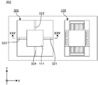
- FIG. 1 is a schematic diagram showing an optical scanning device according to Embodiment 1 of the present invention and a vehicle 150 equipped with the optical scanning device 100, the whole being represented by 100.
- the optical scanning device 100 is typically mounted on a vehicle 150 such as an automobile.
- the optical scanning device 100 includes a light source 101 that emits a beam-shaped laser beam (hereinafter referred to as “light beam”), a light beam emitted from the light source 101 is incident, and transmits a part of the incident light.
- a beam splitter 104 that reflects other portions and a substrate 102 on which the light beam emitted from the light source 101 enters via the beam splitter 104 are provided.
- the substrate 102 includes an acceleration sensor 105 for detecting the acceleration of the optical scanning device 100 and a two-dimensional scanning mirror 106 that can change the direction of the optical axis of the incident light beam.
- the optical scanning device 100 further includes a control unit 103 that controls the attitude of the two-dimensional scanning mirror 106 based on the acceleration detected by the acceleration sensor 105.
- the X axis, the Y axis, and the Z axis are introduced.
- the surface of the substrate 102 extends in the X direction and the Y direction perpendicular to the X direction.
- the Y direction is a direction perpendicular to the paper surface of FIG.
- a direction perpendicular to the X axis and the Y axis is taken as a Z direction.
- the path of the light beam is indicated by a broken line.
- the light source 101 is, for example, a laser diode (LD) element or a light emitting diode element (LED), but is not limited thereto. Further, a collimator lens (not shown) that adjusts the diffused light into a parallel light beam may be provided at the subsequent stage of the light source 101 (between the light source 101 and the beam splitter 104).
- LD laser diode
- LED light emitting diode element
- the substrate 102 is arranged so that the optical axis of the light beam emitted from the light source 101 passes through the center of the two-dimensional scanning mirror 106 via the beam splitter 104.
- the light beam emitted from the light source 101 passes through the beam splitter 104 and enters the center of the two-dimensional scanning mirror 106.
- the light beam reflected by the two-dimensional scanning mirror 106 enters the beam splitter 104 again. At least part of the light incident on the beam splitter 104 is reflected by the beam splitter 104 and emitted from the optical scanning device 100 in the X direction.
- FIG. 2 is a schematic top view of the substrate 102.
- the two-dimensional scanning mirror 106 of the substrate 102 is mounted so as to be rotatable about the X axis, and surrounds the periphery of the mirror unit 111 at a distance from the mirror unit 111 in a plan view.
- a frame 113 mounted rotatably around the Y axis. Both ends of the mirror portion 111 in the Y direction are connected to the frame 113 via beams 120 that are flexible and can be bent in the longitudinal direction. Both outer ends in the X direction of the frame 113 are connected to the substrate 102 via beams 120, respectively.
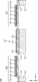
- FIG. 3 is a schematic cross-sectional view of the two-dimensional scanning mirror 106 of the substrate 102 of FIG. 2 as viewed in the III-III direction.
- the two-dimensional scanning mirror 106 includes, for example, a support layer 141 made of non-conductive single crystal silicon, an insulating layer 142 formed on the support layer 141, and an active layer 143 formed on the insulating layer 142.
- An SOI (Silicon-on-insulator) substrate is formed.
- the insulating layer 142 is, for example, a silicon oxide film.
- the active layer 143 is a conductive single crystal silicon layer having conductivity by adding impurities, for example.
- An insulating film 121 is formed on the active layer 143 of the two-dimensional scanning mirror 106.
- a reflective film 115 that reflects light on the surface is formed.
- the reflective film 115 is made of, for example, Au (gold), but is not limited thereto.
- the beam 120 includes a beam foundation 125 that is a part of the active layer 143, an insulating film 121 formed on the beam foundation 125, a first electrode 122 formed on the insulating film 121, and a first electrode 122. And the second electrode 124 formed on the piezoelectric film 123.
- the first electrode 122 is made of, for example, Pt (platinum).
- the piezoelectric film 123 is made of, for example, lead zirconate titanate (PZT).
- the second electrode 124 is made of, for example, Au (gold).
- the first electrode 122 and the second electrode 124 of the beam 120 of the two-dimensional scanning mirror 106 are electrically insulated.
- the first electrode 122 and the second electrode 124 are electrically connected to an external power source (not shown) via separate wirings (not shown).
- the piezoelectric material of the piezoelectric film 123 is pretreated so as to have polarization in the thickness direction (Z-axis direction).
- a downward electric field (the negative direction of the Z axis) is applied to the piezoelectric film 123
- the piezoelectric film 123 extends in the in-plane direction, and the beam 120 is warped so as to be convex upward. Therefore, the end of the beam 120 can be displaced downward.
- an upward electric field (the positive direction of the Z axis) is applied to the piezoelectric film 123, the piezoelectric film 123 contracts in the in-plane direction, and the beam 120 warps to protrude downward. Thereby, the edge part of the beam 120 can be displaced upwards.
- the beam 120 is deformed in the Z direction, and the two-dimensional scanning mirror 106 is moved in the X axis or Y axis.
- Can be rotated around
- the connection part between the beam 120 and the mirror part 111 and the connection part between the beam 120 and the frame 113 are displaced in the Z direction.
- the connection part between the beam 120 and the mirror part 111 is displaced in the Z direction, the mirror part 111 rotates around the X axis.
- the connection part between the beam 120 and the frame 113 is displaced in the Z direction, the mirror part 111 rotates around the Y axis (because the frame 113 rotates around the Y axis).
- the direction of the warp of the beam 120 can be changed by controlling the sign of the applied voltage. Further, the curvature of the warp can be changed by controlling the magnitude of the applied voltage. That is, the deformation of the beam 120 can be controlled by the sign of the applied voltage and the magnitude.
- the mirror part 111 can be rotated around the Y axis by providing the two beams 120 at positions facing each other across the mirror part 111 from the positive and negative directions of the X axis. Furthermore, by providing two beams 120 at positions facing each other across the mirror unit 111 from the positive and negative directions of the Y axis, the mirror unit 111 can be rotated about the X axis independently of the rotation about the Y axis. it can.
- the example in which the mirror unit 111 of the two-dimensional scanning mirror 106 is supported by the four beams 120 and the piezoelectric film 123 is provided on each beam 120 has been described (see FIGS. 2 and 3).
- the number, arrangement, and shape of the beam 120 and the type, arrangement, and shape of the piezoelectric film 123 can be changed as long as the tilt angle of the mirror unit 111 can be changed to change the direction of the optical axis of the light beam.
- the number, arrangement, and shape of the beam 120 and the type, arrangement, and shape of the piezoelectric film 123 can be changed as long as the tilt angle of the mirror unit 111 can be changed to change the direction of the optical axis of the light beam.
- the mechanism for changing the tilt angle of the mirror unit 111 may be any mechanism that can change the direction of the optical axis of the light beam by changing the tilt angle of the mirror unit 111, and is not limited to the one described above.
- the tilt angle of the mirror unit 111 using an electrostatic attraction generated by applying a voltage to the electrode or an electromagnetic force generated by passing a current through a wiring arranged on the substrate while applying a magnetic field. May be changed.
- the shape of the mirror unit 111 of the two-dimensional scanning mirror 106 is a quadrangle in plan view, but is not limited thereto.
- the mirror unit 111 has a mechanical natural resonance frequency (also called a natural frequency) fyc with respect to vibration around the Y axis.
- a mechanical natural resonance frequency also called a natural frequency
- the driving frequency of the signal applied to the piezoelectric film 123 of each beam 120 of the two-dimensional scanning mirror 106 is also controlled so that the mirror 111 (see FIG. 3) of the two-dimensional scanning mirror 106 also resonates around the axis.
- the material, shape and mass of each part of the two-dimensional scanning mirror 106 are designed in accordance with the signal drive frequency so that resonance occurs around the axis. Thereby, compared with the case where resonance does not arise, a big amplitude can be obtained with the same applied voltage.
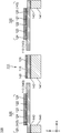
- FIG. 4 is a schematic cross-sectional view of the acceleration sensor 105 of the substrate 102 of FIG. 2 as viewed in the IV-IV direction.
- FIG. 5 is a schematic cross-sectional view of the acceleration sensor 105 of the substrate 102 of FIG. 2 as viewed in the VV direction. 2, 4, and 5, the acceleration sensor 105 of the substrate 102 is disposed so as to sandwich the inertial mass 131 and the inertial mass 131 from both sides in the X direction, and the inertial mass 131 is placed on the surface of the substrate 102.
- Each comb electrode 133 includes a plurality of fixed comb electrodes 134 respectively connected to the substrate 102 and a plurality of movable comb electrodes 135 respectively connected to the inertia mass body 131.
- the fixed comb electrode 134 and the movable comb electrode 135 are arranged in close proximity to each other in the X direction to form a capacitance.
- the fixed comb electrode 134 and the movable comb electrode 135 of the acceleration sensor 105 are electrically insulated.
- the fixed comb electrode 134 and the movable comb electrode 135 are electrically connected to separate conductive substrates (not shown), and bonding pads (not shown) electrically connected to the respective conductive substrates are provided. Via, it is electrically connected to an external electric circuit (not shown).
- the movable comb electrode 135 When the optical scanning device 100 is accelerated or decelerated in the X direction, the movable comb electrode 135 is displaced in the X direction relative to the fixed comb electrode 134 in accordance with the inertial mass body 131. As a result, the capacitance between the fixed comb electrode 134 and the movable comb electrode 135 changes. Since the displacement amount of the inertial mass body 131 depends on the acceleration, the acceleration of the optical scanning device 100 can be detected by measuring the capacitance.
- the acceleration sensor 105 has the fixed comb electrode 134 and the movable comb electrode 135 and detects the acceleration of the optical scanning device 100 based on the change in capacitance.
- the shape of the electrodes is not limited to a comb-like shape, and the number and arrangement of the electrodes are not limited to those described above with reference to FIGS.
- the acceleration detecting means of the optical scanning device 100 is not limited to the one based on the change in capacitance.
- the inertial mass body 131 is supported by a beam made of single crystal silicon, a strain gauge is formed on the beam by means such as impurity diffusion, and the inertial force applied to the inertial mass body 131 using the piezoresistance effect is applied. By detecting, the acceleration of the optical scanning device 100 can be detected.
- the acceleration sensor 105 is disposed so as to sandwich the inertial mass body 131 from both sides in the X direction, and supports the inertial mass body 131 so as to be displaceable in the X direction. It had two beams 132. However, the number, arrangement, and shape of the beams 132 are not limited to those described above, and any beam that can support the inertial mass body 131 so as to be displaceable may be used.
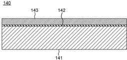
- FIG. 6 is a schematic cross-sectional view of the SOI substrate 140 before processing.
- the SOI substrate 140 includes a support layer 141 made of non-conductive single crystal silicon, an insulating layer 142 formed on the support layer 141, and an active layer 143 formed on the insulating layer 142.
- the insulating layer 142 is, for example, a silicon oxide film.
- the active layer 143 is, for example, a conductive single crystal silicon layer that has conductivity by adding impurities.
- Step 1 An insulating film 121 (for example, a silicon oxide film) is formed on the active layer 143 of the SOI substrate 140 and patterned.
- Step 2 A first electrode 122 (for example, Pt) is formed on the insulating film 121 and patterned.
- Step 3 A piezoelectric film 123 (for example, a PZT film) is formed on the first electrode 122 and patterned.
- Step 4 A second electrode 124 (for example, Au) is formed on the piezoelectric film 123 and patterned.
- Step 5 The support layer 141 and the active layer 143 of the SOI substrate 140 are partially etched.
- Step 6 A desired part of the insulating film 121 is etched.
- the manufacturing method of the optical scanning device 100 is not limited to the processing of the SOI substrate 140, and any method can be used as long as the acceleration sensor 105 and the two-dimensional scanning mirror 106 can be formed on the same substrate.
- a conductive polycrystalline silicon layer may be formed after forming a thermal oxide film on a single crystal silicon substrate by annealing, and then the above steps 1 to 6 may be performed on this substrate.
- the two-dimensional scanning mirror 106 is not limited to a so-called MEMS mirror manufactured by the semiconductor fine processing technique as described above.
- the acceleration sensor 105 is not limited to a MEMS acceleration sensor.
- the acceleration sensor 105 may be a mechanical acceleration sensor composed of a spring and a weight, or an acceleration sensor that optically detects displacement of an inertial mass body 131 (see, for example, FIG. 2).
- the thickness of the mirror portion 111 of the two-dimensional scanning mirror 106 is larger than that of the beam 120 (see FIG. 3). This is to reduce the deflection of the reflective film 115 of the mirror part 111 of the two-dimensional scanning mirror 106 as much as possible.
- the mirror unit 111 only needs to be capable of changing the direction of the optical axis of the light beam by changing the tilt angle.
- the thickness of the mirror unit 111 of the two-dimensional scanning mirror 106 is described above. It is not limited to what you did.
- FIG. 7 is a schematic diagram showing the relationship between the inclination angle of the mirror part 111 of the two-dimensional scanning mirror 106 and the traveling direction of the light beam reflected by the mirror part 111.
- the normal line of the mirror unit 111 is also tilted by ⁇ / 2, so the angle formed by the optical axis of the reflected light and the optical axis of the incident light is ⁇ .
- the traveling direction of the light beam reflected by the mirror unit 111 and directed to the beam splitter 104 moves in the YZ plane. Therefore, the traveling direction of the light beam reflected by the beam splitter 104 and emitted from the optical scanning device 100 in the X direction moves in the XY plane.
- the traveling direction of the light beam emitted from the optical scanning device 100 in the X direction moves in the ZX plane.
- the mirror unit 111 is vibrated around the X axis at a constant frequency, and at a constant frequency. Can be vibrated around the Y axis. By controlling each frequency, scanning with the light beam emitted from the optical scanning device 100 can be performed.
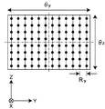
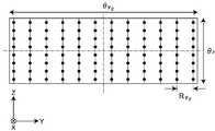
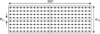
- FIG. 8 is a schematic diagram showing a scanning range (angle) by the light beam emitted from the optical scanning device 100.
- the light beam is emitted from the optical scanning device 100 in the X direction, scans within the range of the maximum scanning angle ⁇ y in the Y-axis direction, and scans within the range of the maximum scanning angle ⁇ z in the Z-axis direction. Therefore, the light beam emitted from the optical scanning device 100 can typically scan within the rectangular area shown in FIG.
- the maximum scanning angles ⁇ y and ⁇ z are controlled by the magnitude and sign of a voltage (hereinafter referred to as “driving voltage”) V applied to the piezoelectric film 123 (see FIG. 3).
- FIG. 9 is a schematic diagram showing an example of a scanning path of a light beam that scans within the scanning range of FIG.
- the scanning points illuminated by the pulsed laser light emitted from the optical scanning device 100 at regular intervals are schematically indicated by black circles.
- the locus of the light beam is shown by a solid line for convenience of explanation.
- the mirror unit 111 of the two-dimensional scanning mirror 106 is rotated around the Y axis, the light beam emitted from the optical scanning device 100 in the X direction moves in the ZX plane and is longitudinally directed toward the paper surface.
- One column in the (main scanning direction) is scanned.
- the mirror unit 111 When the mirror unit 111 is rotated around the X axis, the light beam emitted from the optical scanning device 100 in the X direction moves in the XY plane, and the scanning path of the light beam moves sideways (sub-scanning direction).
- a matrix of scanning points as shown in FIG. 9 is typically realized.
- the vibration frequency around the X axis of the mirror unit 111 of the two-dimensional scanning mirror 106 is fx
- the vibration frequency around the Y axis is fy.
- n is an integer determined by the following equation (3).
- n ⁇ y / Ry (3)
- Ry is an angular interval (hereinafter referred to as “spatial resolution”) between a column (main scanning line) in the matrix of scanning points in FIG.
- Equation (4) is derived from equations (1) to (3).
- the optical scanning device 100 scans in the same direction with a period 1 / fx (that is, periodically scans the same scanning point in FIG. 9 with the light beam). Irradiation).
- the frequency fx of vibration around the X axis of the mirror unit 111 of the two-dimensional scanning mirror 106 is referred to as “drive frequency” or “frame rate”.
- the optical scanning device 100 can scan a light beam
- the optical scanning device 100 can be applied to a distance measuring device that measures the distance between the optical scanning device 100 and an object around it and recognizes the surrounding situation.
- the optical scanning device 100 can measure the distance in the traveling direction and check whether there is an obstacle in the traveling direction.
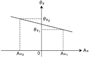
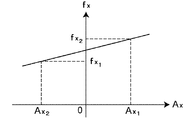
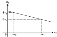
- FIG. 10 shows an example of the relationship between the acceleration Ax and the maximum scanning angle ⁇ y when the maximum scanning angle ⁇ y is adjusted according to the acceleration Ax.
- the maximum scan angle [theta] y is at acceleration Ax 1 in (acceleration) is [theta] y 1, times the acceleration Ax 2 (deceleration) indicates that it is adjusted to the [theta] y 2 (> [theta] y 1) .
- FIG. 11 is a schematic diagram showing a scanning path and a scanning point by a conventional distance measuring device during acceleration (acceleration Ax 1 in FIG. 10).
- the spatial resolution Ry in this case is Ry 1 .
- FIG. 12 is a schematic diagram illustrating a scanning path and a scanning point by a conventional distance measuring device during deceleration (at the time of acceleration Ax 2 in FIG. 10). Spatial resolution Ry in this case is Ry 2.
- the scanning points in the Y direction are sparser and the spatial resolution Ry is worse than that in FIG. 11 showing the case of acceleration (that is, Ry 1 ⁇ Ry 2 ).
- the prior art has a problem that the spatial resolution Ry deteriorates when the maximum scanning angle ⁇ y is widened.
- the optical scanning device 100 controls the drive frequency (frame rate) fx so that the spatial resolution Ry does not deteriorate even if the maximum scanning angle ⁇ y is changed according to the acceleration Ax of the vehicle 150.
- the drive frequency (frame rate) fx is set so that fx ⁇ ⁇ y is constant from the equation (4). Can be controlled. For example, when the maximum scanning angle ⁇ y is doubled, the spatial resolution Ry can be kept constant if the drive frequency (frame rate) fx is halved.
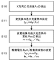
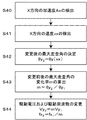
- FIG. 13 is a flowchart showing a method of changing the drive frequency (frame rate) fx according to the acceleration Ax without deteriorating the spatial resolution Ry.
- the drive frequency (frame rate) fx fx 1
- the drive voltage V Vy 1
- the acceleration sensor 105 (see FIGS. 1 and 2) of the optical scanning device 100 detects the acceleration Ax in the X direction.
- the control unit 103 determines the changed maximum scanning angle ⁇ y 2 based on the detected acceleration Ax. For example, when the acceleration Ax is negative (when decelerating), ⁇ y 2 > ⁇ y 1 is set.
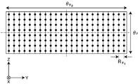
- FIG. 14 is a schematic diagram showing scanning paths and scanning points by the optical scanning device 100 according to Embodiment 1 of the present invention in which the drive frequency fx is adjusted in this way.
- the spatial resolution Ry is Ry 1 , and it can be seen that there is no change from the spatial resolution during acceleration (see FIG. 11).
- the optical scanning device 100 controls the maximum scanning angle ⁇ y of the light beam based on the acceleration Ax, and controls the driving frequency (frame rate) fx to achieve the maximum. Even if the scanning angle ⁇ y is changed, the spatial resolution Ry can be kept constant.
- the spatial resolution Ry is kept constant. For example, when it is desired to detect the behavior of a specific object in the traveling direction at a high frame rate, the spatial resolution Ry is kept constant by controlling the maximum scanning angle ⁇ y based on the target drive frequency (frame rate) fx. Can keep.
- FIG. 15 is a flowchart showing a method of controlling the maximum scanning angle ⁇ y based on the drive frequency (frame rate) fx without deteriorating the spatial resolution Ry.
- the drive frequency (frame rate) fx fx 1
- the drive voltage V Vy 1
- the acceleration sensor 105 (see FIGS. 1 and 2) of the optical scanning device 100 detects an acceleration Ax in the X direction.
- the control unit 103 determines the changed drive frequency (frame rate) fx 2 based on the detected acceleration Ax. For example, as shown in FIG. 16, when acceleration Ax is positive (acceleration), fx 2 > fx 1 is set.
- the acceleration sensor 105 and the two-dimensional scanning mirror 106 are formed on the same substrate 102 (see FIGS. 1 and 2). Therefore, the optical scanning device 100 has an advantage that it is not necessary to adjust the relative position of each other when the optical scanning device 100 is attached to a device such as the vehicle 150 (see FIG. 1).
- the present invention is not limited to this, and the acceleration sensor 105 and the two-dimensional scanning mirror 106 may be formed on different substrates.
- n is not limited to an integer.
- the scanning path of the light beam is a so-called Lissajous figure, and the period in which the light beam illuminates the same scanning point is not 1 / fx but the reciprocal of the least common multiple of fx and fy.
- the effect of suppressing the change in the spatial resolution Ry can be obtained by controlling the drive frequency (frame rate) fx, as described above.
- the traveling direction of the vehicle 150 (see FIG. 1) is the X-axis direction, but is not limited thereto.
- the mirror part 111 of the two-dimensional scanning mirror 106 resonates around the Y axis perpendicular to the traveling direction (X direction) of the vehicle 150, but is not limited to this, and resonates around another direction. Then, it may be rotationally displaced.
- the acceleration sensor 105 detects the acceleration in the traveling direction of the optical scanning device 100.
- the acceleration sensor 105 is not limited to this.
- the acceleration sensor 105 detects the acceleration in the direction orthogonal to the traveling direction of the optical scanning device 100. It may be.
- the acceleration sensor 105 may be capable of detecting acceleration in directions of two or more axes. Thereby, for example, fluctuations in the Y-axis direction and the Z-axis direction orthogonal to the traveling direction of the optical scanning device 100 can be detected, and the maximum scanning angle can be adjusted according to the magnitude of the fluctuation.
- the vibration frequency fy around the Y-axis of the mirror unit 111 of the two-dimensional scanning mirror 106 is set as the specific resonance frequency fyc (see Expression (1)).
- Embodiment 1 of the present invention is not limited to this, and fy may be a frequency in the vicinity of fyc.
- the applied voltage can be converted into vibrations most efficiently.
- fy is close to the resonance frequency fyc, a relatively large amplitude is obtained with the same applied voltage. be able to.
- the maximum scanning angle ⁇ y is uniformly changed with respect to the change in the acceleration Ax of the optical scanning device 100 ( ⁇ y is expressed as a linear function of Ax).
- the first embodiment of the present invention is not limited to this, as long as the maximum scanning angle ⁇ y is determined according to the acceleration Ax.
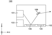
- FIG. 17 is a schematic diagram showing the configuration of the optical scanning device according to the first modification of the first embodiment of the present invention, the whole being represented by 180.
- the beam splitter is not provided, and the light beam emitted from the light source 101 enters the two-dimensional scanning mirror 106 without passing through the beam splitter.
- FIG. 18 is a schematic diagram showing the configuration of the optical scanning device according to the second modification of the first embodiment of the present invention, the whole being represented by 190.
- This modification also does not include a beam splitter, but instead includes a fixed mirror 109 that reflects the light beam incident from the two-dimensional scanning mirror 106.
- the first embodiment of the present invention can achieve the same effect, so that the freedom of member arrangement can be increased.
- the first modification and the second modification can also be applied to a second embodiment, a third embodiment, and a fourth embodiment of the present invention described later.
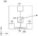
- FIG. FIG. 19 is a schematic diagram showing the configuration of the optical scanning device according to the second embodiment of the present invention, the whole being represented by 200.
- the same components as those in the first embodiment are denoted by the same reference numerals, and the description thereof is omitted.
- the optical scanning device 200 includes an angular velocity sensor 207 instead of an acceleration sensor.
- the angular velocity sensor 207 can detect an angular velocity (hereinafter simply referred to as “angular velocity”) ⁇ z around the vertical axis (Z-axis).
- the angular velocity sensor 207 is provided separately from the substrate 202.
- the second embodiment of the present invention is not limited to this, and the angular velocity sensor 207 may also be formed on the substrate 202 using the MEMS technology.
- the optical scanning device 200 may also be used by being mounted on a vehicle (not shown).
- the distance measuring device mounted on the vehicle scans the distance in the traveling direction with high spatial resolution.
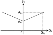
- the vehicle makes a left turn, a right turn, or a curve, it is necessary to widely recognize the surrounding situation. Therefore, it is desirable that the distance measuring device mounted on the vehicle scans a wide range. Therefore, conventionally, as shown in FIG. 20, the maximum scanning angle ⁇ y is reduced when the absolute value of the angular velocity ⁇ z is small, and the maximum scanning angle ⁇ y is increased when the absolute value of the angular velocity ⁇ z is large. Changing the maximum scanning angle ⁇ y according to the angular velocity ⁇ z has been performed.
- FIG. 20 shows an example of the relationship between the angular velocity ⁇ z and the maximum scanning angle ⁇ y when the maximum scanning angle ⁇ y is adjusted according to the angular velocity ⁇ z.
- the angular velocity ⁇ z is zero.
- the angular velocity ⁇ z indicates a positive value.
- the angular velocity ⁇ z shows a negative value.
- the scanning points in the Y direction are sparse and the spatial resolution is deteriorated as compared to FIG. 21 showing the case of going straight.
- the prior art has a problem that the spatial resolution at the time of turning is worse than that at the time of going straight.
- the spatial resolution Ry does not deteriorate even if the maximum scanning angle ⁇ y is changed in accordance with the angular velocity ⁇ z of the vehicle (that is, From equation (4), the drive frequency (frame rate) fx is controlled so that fx ⁇ ⁇ y is constant.
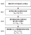
- FIG. 23 is a flowchart showing a method of changing the drive frequency (frame rate) fx according to the angular velocity ⁇ z without deteriorating the spatial resolution Ry.
- the drive frequency (frame rate) fx fx 1
- the drive voltage V Vy 1
- the angular velocity sensor 207 (see FIG. 19) of the optical scanning device 200 detects an angular velocity ⁇ z around the Z axis.
- control unit 103 determines the changed maximum scanning angle ⁇ y 2 based on the detected angular velocity ⁇ z.
- FIG. 24 is a schematic diagram showing scanning paths and scanning points by the optical scanning device 100 according to Embodiment 2 of the present invention in which the drive frequency fx is adjusted in this way.
- the spatial resolution Ry is Ry 1 and has not changed from the spatial resolution during straight travel (see FIG. 21).
- the optical scanning device 200 controls the maximum scanning angle ⁇ y of the light beam based on the angular velocity ⁇ z and controls the driving frequency (frame rate) fx to achieve the maximum. Even if the scanning angle ⁇ y is changed, the spatial resolution Ry can be kept constant.
- the angular velocity sensor 207 detects the angular velocity around the vertical direction of the optical scanning device 200.
- the angular velocity sensor 207 is not limited to this.
- the angular velocity around the axis perpendicular to the vertical direction. May be detected.
- the angular velocity sensor 207 may be capable of detecting angular velocities around two or more axes.
- the angular velocity sensor 207 may detect rotation around an axis in the horizontal plane of the optical scanning device 200.
- the maximum scanning angle ⁇ y changes uniformly with respect to the change in the angular velocity ⁇ z of the optical scanning device 200.
- Embodiment 2 of the present invention is limited to this.
- the maximum scanning angle ⁇ y may be determined according to the angular velocity ⁇ z.
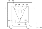
- FIG. FIG. 25 is a schematic diagram showing the configuration of the optical scanning device according to the third embodiment of the present invention, the whole of which is represented by 300.
- the same components as those in the first embodiment or the second embodiment are denoted by the same reference numerals, and the description thereof is omitted.
- the light beam emitted from the light source 101 of the optical scanning device 300 is reflected by the two-dimensional scanning mirror 306 provided on the substrate 302, then reflected by the scanning angle conversion means 308, and emitted from the optical scanning device 300.
- the scanning angle conversion unit 308 has an inverted truncated cone shape with the vertical axis (Z axis) as the central axis, and the light beam is reflected by the conical surface 309 of the scanning angle conversion unit 308.
- FIG. 26 is a schematic top view of the substrate 302.
- the substrate 302 includes an acceleration sensor 105 for detecting the acceleration of the optical scanning device 300 and a two-dimensional scanning mirror 306 that can change the direction of the optical axis of the incident light beam.
- the two-dimensional scanning mirror 306 includes a mirror unit 111 and four beams 321 to 324 that are respectively connected to four points on both ends in the X direction and both ends in the Y direction of the mirror unit 111 and support the mirror unit 111. Both ends in the X direction and both ends in the Y direction of the mirror unit 111 are connected to the substrate 302 via beams 321 to 324, respectively.
- the two-dimensional scanning mirror 306 is not provided with a frame (see the frame 113 in FIG. 2).
- FIG. 27 is a schematic cross-sectional view of the two-dimensional scanning mirror 306 of the substrate 302 of FIG. 26 as viewed in the XXV-XXV direction.
- Beams 321 and 323 (and beams 322 and 324 not shown in FIG. 27) are the same as the beam 120 of the first embodiment described with reference to FIG.
- a second electrode 124 formed on the piezoelectric film 123.
- Sinusoidal voltages having the same frequency and the same amplitude but different phases are applied to the piezoelectric film 123 via the first electrode 122 and the second electrode 124 (FIG. 27) of the beams 321 to 324 (FIG. 26).
- V (t) a sine wave voltage
- V (t) a sine wave whose phase is delayed by 90 degrees ( ⁇ / 2) from V (t) is applied to the piezoelectric film 123 of the beam 322.
- a voltage V (t ⁇ / 2) is applied, and a sine wave voltage V (t ⁇ ) whose phase is delayed by 90 degrees is further applied to the piezoelectric film 123 of the beam 323, and the piezoelectric film 123 of the beam 324 is applied to the piezoelectric film 123.
- the mirror portions are applied by applying the sinusoidal voltages having different phases to the piezoelectric films 123 of the beams 321 to 324 as described above.
- 111 moves so that the normal of the surface of the mirror part 111 performs a precession movement (swing movement) centering on the center of the mirror part 111.
- the normal line at the center of the surface of the mirror part 111 draws an inverted cone having the center of the surface of the mirror part 111 as a vertex.
- the mirror unit 111 swings so that the apex angle of the inverted cone is ⁇ / 2, when the beam light is incident on the substrate 302 vertically, it is reflected as shown by the broken line in FIG.
- the optical axis of the light beam swings so as to draw an inverted cone whose apex angle is ⁇ .
- the mirror unit 111 has a mechanical resonance frequency foc for the swing motion.
- the applied energy can be efficiently converted into vibration.
- the light beam reflected by the mirror unit 111 of the two-dimensional scanning mirror 306 is then reflected by the conical surface 309 of the scanning angle conversion means 308 and emitted from the optical scanning device 300.
- the relationship shown in the following equation (5) is between the angle ⁇ formed by the horizontal plane (XY plane) and the conical surface 309 of the scanning angle conversion means 308 and the apex angle ⁇ of the inverted cone drawn by the optical axis of the light beam. If so, the optical axis of the light beam emitted from the optical scanning device 300 is on a horizontal plane.
- the maximum amplitude V A of the drive voltage V applied to the piezoelectric films 123 (see FIG. 27) of the beams 321 to 324 is changed (changed to V A + ⁇ V A.
- ⁇ V A is referred to as “amplitude change amount”).
- the apex angle ⁇ of the inverted cone drawn by the optical axis of the light beam can be changed.
- scanning can be performed so that the optical axis of the light beam emitted from the optical scanning device 300 moves in the vertical direction from the horizontal plane.
- the optical scanning device 300 according to the third embodiment has an advantage that it can scan the entire circumference in the horizontal direction.
- FIG. 29 is a schematic diagram showing a vehicle 350 on which the optical scanning device 300 is mounted. Since the optical scanning device 300 can scan the entire circumference in the horizontal direction, the optical scanning device 300 can be advantageously applied to a distance measuring device that recognizes the surrounding conditions mounted on the vehicle 350.
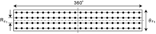
- FIG. 30 is a schematic diagram illustrating an example of a scanning path of a light beam that scans within a scanning range by the optical scanning device 300 according to the third embodiment.
- the scanning points illuminated by the pulsed laser light emitted from the light source 101 at regular intervals are schematically represented by black circles.
- the locus of the light beam is indicated by a solid line for convenience of explanation.
- the control unit 103 (see FIGS. 25 and 29) is configured so that the piezoelectric films 123 (see FIG. 27) of the beams 321 to 324 so that the mirror unit 111 of the two-dimensional scanning mirror 306 performs a swing motion at a specific resonance frequency foc. ) Is applied with a sinusoidal drive voltage V.
- the maximum amplitude V A of the drive voltage V is controlled to increase or decrease at the frequency fr (hereinafter, this frequency is referred to as “amplitude change frequency” or “frame rate”). Since the optical scanning device 300 can scan the entire circumference in the horizontal direction, the maximum horizontal scanning angle is 360 °. The matrix of scanning points in FIG. 30 is obtained in this way.
- the maximum scanning angle ⁇ z is changed by changing the maximum amplitude V A of the drive voltage V in accordance with the acceleration Ax in the traveling direction of the vehicle 350 (see FIG. 29).
- the maximum scanning angle ⁇ z is increased from ⁇ z 1 in FIG. 30 to ⁇ z 2 (> ⁇ z 1 )
- the frequency fr of the amplitude change is not changed, the scanning path of the light beam is as shown in FIG.
- FIG. 31 compared with FIG. 30 showing the case where the maximum scanning angle ⁇ z is small, the scanning points in the Z direction become sparse and the spatial resolution Rz deteriorates (compared to the spatial resolution Rz 1 in FIG. 30). spatial resolution Rz 2 of 31 is getting worse).
- the following equation (6) is used so that the spatial resolution Rz does not deteriorate even if the maximum scanning angle ⁇ z is changed according to the acceleration Ax of the vehicle 350.
- the frequency (frame rate) fr of amplitude change is controlled.
- FIG. 32 is a flowchart showing a method of changing the frequency (frame rate) fr of the amplitude change according to the acceleration Ax without deteriorating the spatial resolution Rz.
- the amplitude change frequency (frame rate) fr fr 1
- the amplitude change amount ⁇ V A ⁇ V A1
- the maximum scanning angle ⁇ z ⁇ z 1 .
- the acceleration sensor 105 see FIG. 25
- the optical scanning device 300 detects the acceleration Ax in the X direction.
- control unit 103 determines the maximum scan angle [theta] z 2 after the change.
- FIG. 33 is a schematic diagram showing scanning paths and scanning points by the optical scanning device 300 according to the third embodiment of the present invention in which the amplitude change fr is adjusted in this way.
- the spatial resolution Rz is Rz 1 and has not changed from the spatial resolution before the change (see FIG. 30).
- the optical scanning device 300 including the acceleration sensor 105 has been described above, the optical scanning device 300 according to the third embodiment of the present invention includes the angular velocity sensor described in the second embodiment, and the maximum scanning angle based on the angular velocity. You may determine (theta) z and the frequency (frame rate) fr of an amplitude change.
- the optical scanning device 300 controls the maximum scanning angle ⁇ z of the light beam based on the acceleration or the angular velocity, and also controls the driving frequency (frame rate) fr. Even if the maximum scanning angle ⁇ z is changed, the spatial resolution Rz can be kept constant.
- FIG. 34 is a schematic diagram showing the configuration of the optical scanning device according to the fourth embodiment of the present invention, the whole being represented by 400.
- the same reference numerals are given to the same configurations as those of the first embodiment, the second embodiment, or the third embodiment, and the description thereof is omitted.
- the optical scanning device 400 includes a control unit 403 that controls the attitude of the two-dimensional scanning mirror 106 based on the speed.
- the control unit 403 integrates the X-direction acceleration Ax detected by the acceleration sensor 105 to derive the X-direction velocity vx.
- the optical scanning device 400 may be mounted on a vehicle (not shown) and used.
- a distance measuring device mounted on the vehicle scans a distant place with high spatial resolution.
- a low speed for example, when driving slowly, there is a high possibility that the traveling direction of the vehicle suddenly changes due to a right or left turn, etc. It is desirable to scan.
- FIG. 35 shows an example of the relationship between the speed vx and the maximum scanning angle ⁇ y when the maximum scanning angle ⁇ y is adjusted according to the speed vx.
- the maximum scan angle [theta] y is, at the speed vx 1 (at high speed) to the [theta] y 1, at the speed vx 2 (at a low speed, vx 2 ⁇ vx 1) is [theta] y 2 is adjusted to (> [theta] y 1) Which indicates that.
- the scanning path and the scanning point at the time of high speed are the same as those in FIG. 11 of the first embodiment.
- the scanning path and scanning point by the conventional distance measuring device at low speed are the same as those in FIG.
- the spatial resolution at low speed is worse than the spatial resolution at high speed.
- the spatial resolution Ry is not deteriorated even if the maximum scanning angle ⁇ y is changed according to the vehicle speed vx (for example, from the equation (4), fx ⁇ ⁇ y is The drive frequency (frame rate) fx is controlled so as to be constant.
- FIG. 36 is a flowchart showing a method of changing the drive frequency (frame rate) fx according to the speed vx without deteriorating the spatial resolution Ry.
- the acceleration Ax in the X-axis direction is detected by the acceleration sensor of the optical scanning device 400.
- the velocity vx in the X-axis direction is calculated by time integration of Ax.
- step S42 the control unit 403, based on the speed vx which is calculated to determine the maximum scan angle [theta] y 2 after the change.
- the control unit 403 calculates the speed by the control unit by the time integration of the acceleration Ax detected by the acceleration sensor.
- the present invention is not limited to this, and the speed information can be obtained.
- the optical scanning device 400 may include a speed sensor (not shown), and the speed may be detected by the speed sensor.
- the speed sensor may obtain speed information from the rotational speed of the axle, for example.
- the optical scanning device 400 controls the maximum scanning angle ⁇ y of the light beam based on the speed vx, and controls the driving frequency (frame rate) fx to achieve the maximum. Even if the scanning angle ⁇ y is changed, the spatial resolution Ry can be kept constant.
- Embodiment 4 of the present invention is not limited to this, and depends on the speed vx. As long as the maximum scanning angle ⁇ y is determined.
- Optical scanning device 101 light source, 102 substrate, 103 control unit, 104 beam splitter, 105 acceleration sensor, 106 two-dimensional scanning mirror, 109 fixed mirror, 111 mirror unit, 113 frame, 115 reflective film, 120 beam, 121 insulating film, 122 first electrode, 123 piezoelectric film, 124 second electrode, 125 beam foundation, 131 inertia mass body, 132 beam, 133 comb electrode, 134 fixed comb electrode, 135 movable comb electrode, 140 SOI substrate, 141 support layer, 142 insulating layer, 143 active layer, 150 vehicle, 202 substrate, 207 angular velocity sensor, 302 substrate, 306 two-dimensional scanning mirror, 308 scanning angle conversion means, 321 to 324 beam, 350 vehicle.
Abstract
La présente invention concerne un dispositif de balayage optique 100 capable de maintenir une résolution spatiale fixe même lorsque la plage de balayage est variable. Le dispositif de balayage optique 100 comprend : une source de lumière 101 pour émettre de la lumière ; un miroir de balayage 106 pour réfléchir la lumière entrant à partir de la source de lumière sur la surface de réflexion de celle-ci, le miroir de balayage 106 étant apte à créer des oscillations mutuellement indépendantes autour d'un premier axe traversant la surface de réflexion et un second axe perpendiculaire au premier axe et traversant la surface de réflexion ; et une unité de commande 103 pour balayer la lumière réfléchie par la surface de réflexion du miroir de balayage 106 par commande d'une première fréquence et d'une première amplitude de l'oscillation autour du premier axe du miroir de balayage 106 et d'une seconde fréquence et d'une seconde amplitude de l'oscillation autour du second axe. L'unité de commande 103 commande la seconde fréquence sur la base de l'angle de balayage maximal le long d'une direction de sous-balayage.
Priority Applications (4)
| Application Number | Priority Date | Filing Date | Title |
|---|---|---|---|
| EP18909458.4A EP3767367A4 (fr) | 2018-03-13 | 2018-12-17 | Dispositif de balayage optique et son procédé de commande |
| US16/964,402 US20210011282A1 (en) | 2018-03-13 | 2018-12-17 | Optical scanning device and method of control therefor |
| JP2020505593A JP6789438B2 (ja) | 2018-03-13 | 2018-12-17 | 光走査装置およびその制御方法 |
| CN201880090386.6A CN111819486A (zh) | 2018-03-13 | 2018-12-17 | 光扫描装置及其控制方法 |
Applications Claiming Priority (2)
| Application Number | Priority Date | Filing Date | Title |
|---|---|---|---|
| JP2018-045774 | 2018-03-13 | ||
| JP2018045774 | 2018-03-13 |
Publications (1)
| Publication Number | Publication Date |
|---|---|
| WO2019176204A1 true WO2019176204A1 (fr) | 2019-09-19 |
Family
ID=67906663
Family Applications (1)
| Application Number | Title | Priority Date | Filing Date |
|---|---|---|---|
| PCT/JP2018/046305 WO2019176204A1 (fr) | 2018-03-13 | 2018-12-17 | Dispositif de balayage optique et son procédé de commande |
Country Status (5)
| Country | Link |
|---|---|
| US (1) | US20210011282A1 (fr) |
| EP (1) | EP3767367A4 (fr) |
| JP (1) | JP6789438B2 (fr) |
| CN (1) | CN111819486A (fr) |
| WO (1) | WO2019176204A1 (fr) |
Cited By (4)
| Publication number | Priority date | Publication date | Assignee | Title |
|---|---|---|---|---|
| CN111508383A (zh) * | 2020-04-23 | 2020-08-07 | 歌尔光学科技有限公司 | 成像方法、成像装置及计算机可读存储介质 |
| JP6827601B1 (ja) * | 2020-02-19 | 2021-02-10 | 三菱電機株式会社 | 光反射装置およびそれを備えた測距装置 |
| JP6833127B1 (ja) * | 2020-03-26 | 2021-02-24 | 三菱電機株式会社 | 光走査装置、光走査装置の制御方法、及び測距装置 |
| WO2023053840A1 (fr) * | 2021-09-28 | 2023-04-06 | 富士フイルム株式会社 | Dispositif de balayage optique |
Families Citing this family (2)
| Publication number | Priority date | Publication date | Assignee | Title |
|---|---|---|---|---|
| CN113687387B (zh) * | 2021-09-07 | 2024-03-01 | 广州大学 | 一种激光雷达扫描装置以及激光雷达扫描方法 |
| JP2023144664A (ja) * | 2022-03-28 | 2023-10-11 | 富士フイルム株式会社 | 光走査装置、光走査装置の駆動方法、及び測距装置 |
Citations (6)
| Publication number | Priority date | Publication date | Assignee | Title |
|---|---|---|---|---|
| JPH11153664A (ja) * | 1997-09-30 | 1999-06-08 | Sumitomo Electric Ind Ltd | 繰り返しパルス光を利用した物体検知装置 |
| JP2000075030A (ja) * | 1998-08-27 | 2000-03-14 | Aisin Seiki Co Ltd | スキャン型レーザーレーダ装置 |
| JP2015090463A (ja) * | 2013-11-07 | 2015-05-11 | リコー光学株式会社 | 2次元走査型レーザビーム放射装置 |
| JP2016090268A (ja) | 2014-10-30 | 2016-05-23 | 株式会社デンソー | 車両用光飛行型測距装置 |
| WO2016153687A1 (fr) * | 2015-03-25 | 2016-09-29 | Google Inc. | Véhicule ayant de multiples dispositifs de détection et télémétrie par la lumière (lidars) |
| US20170307736A1 (en) * | 2016-04-22 | 2017-10-26 | OPSYS Tech Ltd. | Multi-Wavelength LIDAR System |
Family Cites Families (12)
| Publication number | Priority date | Publication date | Assignee | Title |
|---|---|---|---|---|
| US7732751B2 (en) * | 2005-06-13 | 2010-06-08 | Arete' Associates | Optical systems and methods using microelectromechanical-systems mirrors exceeding thirty microns |
| US7262895B2 (en) * | 2005-06-14 | 2007-08-28 | Lexmark International, Inc. | Determining operating point of feedback controller applied to operation of oscillating scanning device |
| US8050863B2 (en) * | 2006-03-16 | 2011-11-01 | Gray & Company, Inc. | Navigation and control system for autonomous vehicles |
| JP4881073B2 (ja) * | 2006-05-30 | 2012-02-22 | キヤノン株式会社 | 光偏向器、及びそれを用いた光学機器 |
| JP5304380B2 (ja) * | 2008-07-23 | 2013-10-02 | 株式会社リコー | 光走査装置、これを用いた画像投影装置、ヘッドアップディスプレイ装置および携帯電話機 |
| DE102008055159A1 (de) * | 2008-12-29 | 2010-07-01 | Robert Bosch Gmbh | Adaptive Winkel- und Leistungsanpassung bei 3D-Mikrospiegel-Lidar |
| JP4620789B1 (ja) * | 2009-07-16 | 2011-01-26 | シナノケンシ株式会社 | 光走査装置 |
| EP2339367A1 (fr) * | 2009-12-17 | 2011-06-29 | Siemens Aktiengesellschaft | Appareil à balayage laser |
| WO2015108710A1 (fr) * | 2014-01-20 | 2015-07-23 | Apple Inc. | Détection de position de miroir utilisant la frange de distorsion de champs électriques |
| JP6417833B2 (ja) * | 2014-10-01 | 2018-11-07 | 富士通株式会社 | レーザ測距装置、プログラム及びレーザ測距装置の補正方法 |
| DE102015109160A1 (de) * | 2015-06-10 | 2016-12-15 | Valeo Schalter Und Sensoren Gmbh | Fahrerassistenzsystem für ein Kraftfahrzeug, Kraftfahrzeug sowie Verfahren |
| KR101877388B1 (ko) * | 2016-07-21 | 2018-07-11 | 엘지전자 주식회사 | 차량용 라이다 장치 |
-
2018
- 2018-12-17 CN CN201880090386.6A patent/CN111819486A/zh active Pending
- 2018-12-17 WO PCT/JP2018/046305 patent/WO2019176204A1/fr unknown
- 2018-12-17 EP EP18909458.4A patent/EP3767367A4/fr not_active Withdrawn
- 2018-12-17 US US16/964,402 patent/US20210011282A1/en not_active Abandoned
- 2018-12-17 JP JP2020505593A patent/JP6789438B2/ja active Active
Patent Citations (6)
| Publication number | Priority date | Publication date | Assignee | Title |
|---|---|---|---|---|
| JPH11153664A (ja) * | 1997-09-30 | 1999-06-08 | Sumitomo Electric Ind Ltd | 繰り返しパルス光を利用した物体検知装置 |
| JP2000075030A (ja) * | 1998-08-27 | 2000-03-14 | Aisin Seiki Co Ltd | スキャン型レーザーレーダ装置 |
| JP2015090463A (ja) * | 2013-11-07 | 2015-05-11 | リコー光学株式会社 | 2次元走査型レーザビーム放射装置 |
| JP2016090268A (ja) | 2014-10-30 | 2016-05-23 | 株式会社デンソー | 車両用光飛行型測距装置 |
| WO2016153687A1 (fr) * | 2015-03-25 | 2016-09-29 | Google Inc. | Véhicule ayant de multiples dispositifs de détection et télémétrie par la lumière (lidars) |
| US20170307736A1 (en) * | 2016-04-22 | 2017-10-26 | OPSYS Tech Ltd. | Multi-Wavelength LIDAR System |
Non-Patent Citations (1)
| Title |
|---|
| See also references of EP3767367A4 |
Cited By (6)
| Publication number | Priority date | Publication date | Assignee | Title |
|---|---|---|---|---|
| JP6827601B1 (ja) * | 2020-02-19 | 2021-02-10 | 三菱電機株式会社 | 光反射装置およびそれを備えた測距装置 |
| WO2021166096A1 (fr) * | 2020-02-19 | 2021-08-26 | 三菱電機株式会社 | Dispositif de réflexion de lumière et appareil de mesure de distance pourvu de ce dernier |
| JP6833127B1 (ja) * | 2020-03-26 | 2021-02-24 | 三菱電機株式会社 | 光走査装置、光走査装置の制御方法、及び測距装置 |
| WO2021192161A1 (fr) * | 2020-03-26 | 2021-09-30 | 三菱電機株式会社 | Dispositif de balayage optique, procédé de commande de dispositif de balayage optique et dispositif de mesure de distance |
| CN111508383A (zh) * | 2020-04-23 | 2020-08-07 | 歌尔光学科技有限公司 | 成像方法、成像装置及计算机可读存储介质 |
| WO2023053840A1 (fr) * | 2021-09-28 | 2023-04-06 | 富士フイルム株式会社 | Dispositif de balayage optique |
Also Published As
| Publication number | Publication date |
|---|---|
| EP3767367A1 (fr) | 2021-01-20 |
| JP6789438B2 (ja) | 2020-11-25 |
| EP3767367A4 (fr) | 2021-05-12 |
| CN111819486A (zh) | 2020-10-23 |
| US20210011282A1 (en) | 2021-01-14 |
| JPWO2019176204A1 (ja) | 2020-10-08 |
Similar Documents
| Publication | Publication Date | Title |
|---|---|---|
| WO2019176204A1 (fr) | Dispositif de balayage optique et son procédé de commande | |
| US10330922B2 (en) | Biaxial optical deflector including multiple mirror units, laser radar system, and manufacturing method | |
| US10914939B2 (en) | MEMS reflector system | |
| US8345340B2 (en) | Method of adjusting a resonance frequency of an optical scanning device | |
| US9323048B2 (en) | Optical deflector including meander-type piezoelectric actuators coupled by crossing bars therebetween | |
| JP2017520020A (ja) | 微小光学電気機械デバイスおよびその製造方法 | |
| JP2008295174A (ja) | 揺動装置、同装置を用いた光走査装置、映像表示装置、及び揺動装置の制御方法 | |
| US11467259B2 (en) | Optical scanning apparatus, method for controlling same, and vehicle | |
| US20230139572A1 (en) | Optical scanning device and method of driving micromirror device | |
| WO2012176492A1 (fr) | Actionneur d'entraînement par résonance, micro-dispositif de balayage et appareil optique | |
| JP6369357B2 (ja) | 走査装置 | |
| EP4286916A1 (fr) | Dispositif de balayage optique et procédé d'entraînement d'un dispositif à micromiroir | |
| WO2022259912A1 (fr) | Dispositif de balayage optique et appareil électronique | |
| JP6732651B2 (ja) | ミラーデバイスおよび光走査装置 | |
| WO2022191046A1 (fr) | Actionneur de miroir | |
| WO2020194691A1 (fr) | Dispositif de balayage optique et son procédé de commande | |
| JP7247553B2 (ja) | 可動装置、画像投影装置、ヘッドアップディスプレイ、レーザヘッドランプ、ヘッドマウントディスプレイ、物体認識装置、及び車両 | |
| JP2023005225A (ja) | 半導体デバイスおよび半導体デバイスの製造方法 | |
| JP2022146781A (ja) | 光偏向器、画像投影装置、ヘッドアップディスプレイ、レーザヘッドランプ、ヘッドマウントディスプレイ、距離測定装置及び移動体 | |
| JP2008224807A (ja) | Memsデバイス | |
| JP4793284B2 (ja) | 共振周波数調整装置および共振周波数調整方法 | |
| JP2010234455A (ja) | Memsデバイス |
Legal Events
| Date | Code | Title | Description |
|---|---|---|---|
| 121 | Ep: the epo has been informed by wipo that ep was designated in this application |
Ref document number: 18909458 Country of ref document: EP Kind code of ref document: A1 |
|
| ENP | Entry into the national phase |
Ref document number: 2020505593 Country of ref document: JP Kind code of ref document: A |
|
| NENP | Non-entry into the national phase |
Ref country code: DE |
|
| ENP | Entry into the national phase |
Ref document number: 2018909458 Country of ref document: EP Effective date: 20201013 |