EP3767367A1 - Dispositif de balayage optique et son procédé de commande - Google Patents
Dispositif de balayage optique et son procédé de commande Download PDFInfo
- Publication number
- EP3767367A1 EP3767367A1 EP18909458.4A EP18909458A EP3767367A1 EP 3767367 A1 EP3767367 A1 EP 3767367A1 EP 18909458 A EP18909458 A EP 18909458A EP 3767367 A1 EP3767367 A1 EP 3767367A1
- Authority
- EP
- European Patent Office
- Prior art keywords
- scanning
- scanning device
- optical scanning
- frequency
- axis
- Prior art date
- Legal status (The legal status is an assumption and is not a legal conclusion. Google has not performed a legal analysis and makes no representation as to the accuracy of the status listed.)
- Withdrawn
Links
Images


Classifications
-
- G—PHYSICS
- G02—OPTICS
- G02B—OPTICAL ELEMENTS, SYSTEMS OR APPARATUS
- G02B26/00—Optical devices or arrangements for the control of light using movable or deformable optical elements
- G02B26/08—Optical devices or arrangements for the control of light using movable or deformable optical elements for controlling the direction of light
- G02B26/10—Scanning systems
- G02B26/101—Scanning systems with both horizontal and vertical deflecting means, e.g. raster or XY scanners
-
- B—PERFORMING OPERATIONS; TRANSPORTING
- B81—MICROSTRUCTURAL TECHNOLOGY
- B81B—MICROSTRUCTURAL DEVICES OR SYSTEMS, e.g. MICROMECHANICAL DEVICES
- B81B3/00—Devices comprising flexible or deformable elements, e.g. comprising elastic tongues or membranes
-
- B—PERFORMING OPERATIONS; TRANSPORTING
- B81—MICROSTRUCTURAL TECHNOLOGY
- B81B—MICROSTRUCTURAL DEVICES OR SYSTEMS, e.g. MICROMECHANICAL DEVICES
- B81B3/00—Devices comprising flexible or deformable elements, e.g. comprising elastic tongues or membranes
- B81B3/0064—Constitution or structural means for improving or controlling the physical properties of a device
- B81B3/0083—Optical properties
-
- B—PERFORMING OPERATIONS; TRANSPORTING
- B81—MICROSTRUCTURAL TECHNOLOGY
- B81B—MICROSTRUCTURAL DEVICES OR SYSTEMS, e.g. MICROMECHANICAL DEVICES
- B81B7/00—Microstructural systems; Auxiliary parts of microstructural devices or systems
- B81B7/04—Networks or arrays of similar microstructural devices
-
- G—PHYSICS
- G01—MEASURING; TESTING
- G01S—RADIO DIRECTION-FINDING; RADIO NAVIGATION; DETERMINING DISTANCE OR VELOCITY BY USE OF RADIO WAVES; LOCATING OR PRESENCE-DETECTING BY USE OF THE REFLECTION OR RERADIATION OF RADIO WAVES; ANALOGOUS ARRANGEMENTS USING OTHER WAVES
- G01S17/00—Systems using the reflection or reradiation of electromagnetic waves other than radio waves, e.g. lidar systems
- G01S17/86—Combinations of lidar systems with systems other than lidar, radar or sonar, e.g. with direction finders
-
- G—PHYSICS
- G01—MEASURING; TESTING
- G01S—RADIO DIRECTION-FINDING; RADIO NAVIGATION; DETERMINING DISTANCE OR VELOCITY BY USE OF RADIO WAVES; LOCATING OR PRESENCE-DETECTING BY USE OF THE REFLECTION OR RERADIATION OF RADIO WAVES; ANALOGOUS ARRANGEMENTS USING OTHER WAVES
- G01S17/00—Systems using the reflection or reradiation of electromagnetic waves other than radio waves, e.g. lidar systems
- G01S17/88—Lidar systems specially adapted for specific applications
- G01S17/93—Lidar systems specially adapted for specific applications for anti-collision purposes
- G01S17/931—Lidar systems specially adapted for specific applications for anti-collision purposes of land vehicles
-
- G—PHYSICS
- G01—MEASURING; TESTING
- G01S—RADIO DIRECTION-FINDING; RADIO NAVIGATION; DETERMINING DISTANCE OR VELOCITY BY USE OF RADIO WAVES; LOCATING OR PRESENCE-DETECTING BY USE OF THE REFLECTION OR RERADIATION OF RADIO WAVES; ANALOGOUS ARRANGEMENTS USING OTHER WAVES
- G01S7/00—Details of systems according to groups G01S13/00, G01S15/00, G01S17/00
- G01S7/48—Details of systems according to groups G01S13/00, G01S15/00, G01S17/00 of systems according to group G01S17/00
- G01S7/481—Constructional features, e.g. arrangements of optical elements
- G01S7/4817—Constructional features, e.g. arrangements of optical elements relating to scanning
-
- G—PHYSICS
- G01—MEASURING; TESTING
- G01S—RADIO DIRECTION-FINDING; RADIO NAVIGATION; DETERMINING DISTANCE OR VELOCITY BY USE OF RADIO WAVES; LOCATING OR PRESENCE-DETECTING BY USE OF THE REFLECTION OR RERADIATION OF RADIO WAVES; ANALOGOUS ARRANGEMENTS USING OTHER WAVES
- G01S7/00—Details of systems according to groups G01S13/00, G01S15/00, G01S17/00
- G01S7/48—Details of systems according to groups G01S13/00, G01S15/00, G01S17/00 of systems according to group G01S17/00
- G01S7/497—Means for monitoring or calibrating
-
- G—PHYSICS
- G02—OPTICS
- G02B—OPTICAL ELEMENTS, SYSTEMS OR APPARATUS
- G02B26/00—Optical devices or arrangements for the control of light using movable or deformable optical elements
- G02B26/08—Optical devices or arrangements for the control of light using movable or deformable optical elements for controlling the direction of light
- G02B26/0816—Optical devices or arrangements for the control of light using movable or deformable optical elements for controlling the direction of light by means of one or more reflecting elements
- G02B26/0833—Optical devices or arrangements for the control of light using movable or deformable optical elements for controlling the direction of light by means of one or more reflecting elements the reflecting element being a micromechanical device, e.g. a MEMS mirror, DMD
-
- G—PHYSICS
- G02—OPTICS
- G02B—OPTICAL ELEMENTS, SYSTEMS OR APPARATUS
- G02B26/00—Optical devices or arrangements for the control of light using movable or deformable optical elements
- G02B26/08—Optical devices or arrangements for the control of light using movable or deformable optical elements for controlling the direction of light
- G02B26/10—Scanning systems
- G02B26/105—Scanning systems with one or more pivoting mirrors or galvano-mirrors
Definitions
- the present invention relates to an optical scanning device and a method of control therefor and, more particularly, to an optical scanning device capable of scanning a wide area with high spatial resolution and a method of control therefor.
- Patent Document 1 discloses a light flight type distance measuring device for a vehicle capable of controlling a scanning range based on vehicle information such as a vehicle speed in a distance measuring device mounted on a vehicle.
- Patent Document 1 JP 2016-090268 A
- a distance measuring device capable of expanding a scanning range by changing a maximum scan angle ⁇ described in Patent Document 1 has a problem that spatial resolution is reduced when the scanning range is expanded.
- An object of the present invention is to provide an optical scanning device capable of optical scanning without reducing the spatial resolution even when the scanning range is expanded.
- An embodiment of the present invention provides an optical scanning device comprising: a light source emitting a light; a scanning mirror that includes a reflecting plane reflecting a light entering from the light source and that is allowed to oscillate independently around each of a first axis extending in the reflecting plane and a second axis orthogonal to the first axis and extending in the reflecting plane; and a controller controlling the scanning mirror in terms of a first frequency and a first amplitude of oscillation around the first axis as well as a second frequency and a second amplitude of oscillation around the second axis for scanning with the light reflected by the reflecting plane of the scanning mirror, the optical scanning device scanning, with the light emitted from the light source, the inside of a scanning range defined by a maximum scanning angle in a main scanning direction changing in accordance with the first amplitude and a maximum scanning angle in a sub-scanning direction orthogonal to the main scanning direction and changing in accordance with the second amplitude.
- the controller controls the second frequency based on the
- the optical scanning device capable of preventing a reduction in spatial resolution can be obtained by controlling a frame rate based on information such as acceleration and angular velocity.
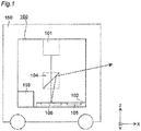
- FIG. 1 is a schematic drawing showing an optical scanning device according to a first embodiment of the present invention, which is generally denoted by 100, and a vehicle 150 equipped with the optical scanning device 100. As shown in FIG. 1 , the optical scanning device 100 is typically mounted on the vehicle 150 such as an automobile.
- the optical scanning device 100 includes a light source 101 emitting a beam-shaped laser beam (hereinafter referred to as "light beam"), a beam splitter 104 on which the light beam emitted from the light source 101 is made incident and that transmits a portion of the incident light while reflecting the other portion, and a substrate 102 on which the light beam emitted from the light source 101 is made incident via the beam splitter 104.
- light beam a beam-shaped laser beam
- the substrate 102 includes an acceleration sensor 105 for detecting the acceleration of the optical scanning device 100 and a two-dimensional scanning mirror 106 capable of changing a direction of an optical axis of the incident light beam.
- the optical scanning device 100 further includes a controller 103 controlling an attitude of the two-dimensional scanning mirror 106 based on the acceleration detected by the acceleration sensor 105.
- an X axis, a Y axis, and a Z axis are introduced for convenience of description.
- a surface of the substrate 102 extends in the X direction and the Y direction perpendicular to the X direction.
- the Y direction is a direction perpendicular to the plane of FIG. 1 .
- the Z direction is defined as a direction perpendicular to the X axis and the Y axis.
- a path of the light beam is indicated by a broken line.
- the light source 101 is a laser diode (LD) element or a light-emitting diode element (LED); however, the present invention is not limited thereto.
- a collimator lens (not shown) adjusting a diffused light into a parallel light flux may be disposed on a subsequent stage of the light source 101 (between the light source 101 and the beam splitter 104).
- the substrate 102 is arranged such that the optical axis of the light beam emitted from the light source 101 passes through the center of the two-dimensional scanning mirror 106 via the beam splitter 104.
- the light beam emitted from the light source 101 passes through the beam splitter 104 and enters the center of the two-dimensional scanning mirror 106.
- the light beam reflected by the two-dimensional scanning mirror 106 enters the beam splitter 104 again. At least a portion of the light entering the beam splitter 104 is reflected by the beam splitter 104 and emitted from the optical scanning device 100 in the X direction.
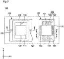
- FIG. 2 is a schematic top view of the substrate 102.
- the two-dimensional scanning mirror 106 of the substrate 102 includes a mirror part 111 reflecting light and attached rotatably around the X-axis and a frame 113 attached rotatably around the Y axis to surround a periphery of the mirror part 111 at a distance from the mirror part 111 in planar view.
- Both ends in the Y direction of the mirror part 111 are respectively connected to the frame 113 via beams 120 having flexibility allowing bending in a longitudinal direction. Both outer ends in the X direction of the frame 113 are respectively connected via the beams 120 to the substrate 102.
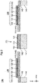
- FIG. 3 is a schematic cross-sectional view of the two-dimensional scanning mirror 106 of the substrate 102 of FIG. 2 as viewed in a direction III-III.
- the two-dimensional scanning mirror 106 is formed on an SOI (silicon on insulator) substrate composed of a support layer 141 made of non-conductive single-crystal silicon, an insulating layer 142 formed on the support layer 141, and an active layer 143 formed on the insulating layer 142.
- the insulating layer 142 is a silicon oxide film, for example.
- the active layer 143 is a conductive single-crystal silicon layer having conductivity due to addition of impurities, for example.
- An insulating film 121 is formed on the active layer 143 of the two-dimensional scanning mirror 106.
- a reflection film 115 reflecting light on a surface is formed on the insulating film 121 of the mirror part 111.
- the reflection film 115 is made of, for example, Au (gold); however, the present invention is not limited thereto.
- the beams 120 are each composed of a beam base 125 that is a portion of the active layer 143, the insulating film 121 formed on the beam base 125, a first electrode 122 formed on the insulating film 121, a piezoelectric film 123 formed on the first electrode 122, and a second electrode 124 formed on the piezoelectric film 123.
- the first electrode 122 is made of Pt (platinum), for example.
- the piezoelectric film 123 is made of lead zirconate titanate (PZT), for example.
- the second electrode 124 is made of Au (gold), for example.
- the first electrode 122 and the second electrode 124 of the beam 120 of the two-dimensional scanning mirror 106 are electrically insulated.
- the first electrode 122 and the second electrode 124 are respectively electrically connected via separate wirings (not shown) to an external power supply (not shown).
- a piezoelectric material of the piezoelectric film 123 is pre-treated to have polarization in a thickness direction (Z-axis direction).
- Z-axis direction a thickness direction
- the piezoelectric film 123 extends in an in-plane direction, and the beam 120 warps into an upward convex shape. Therefore, an end portion of the beam 120 can be displaced downward.
- the beam 120 is deformed in the Z direction to rotate the two-dimensional scanning mirror 106 around the X-axis or the Y-axis.
- a connection portion between the beam 120 and the mirror part 111, and a connection portion between the beam 120 and the frame 113 are displaced in the Z direction.
- connection portion between the beam 120 and the mirror part 111 When the connection portion between the beam 120 and the mirror part 111 is displaced in the Z direction, the mirror part 111 rotates around the X axis. When the connection portion between the beam 120 and the frame 113 is displaced in the Z direction, the mirror part 111 rotates around the Y axis (since the frame 113 rotates around the Y axis).
- the direction of warpage of the beam 120 can be changed by controlling the sign of the applied voltage. Additionally, the curvature of the warpage can be changed by controlling the magnitude of the applied voltage. Therefore, the deformation of the beam 120 can be controlled by the polarity and the magnitude of the applied voltage.
- the mirror part 111 By disposing the two beams 120 at positions opposite to each other across the mirror part 111 in the positive and negative directions of the X axis, the mirror part 111 can be rotated around the Y axis. Furthermore, by disposing the two beams 120 at positions opposite to each other across the mirror part 111 in the positive and negative directions of the X axis, the mirror part 111 can be rotated around the X axis independently of the rotation around the Y axis.
- the mirror part 111 of the two-dimensional scanning mirror 106 is supported by the four beams 120, and the piezoelectric film 123 is disposed on each of the beams 120 (see FIGS. 2 and 3 ).
- the number, arrangement, and shape of the beams 120 and the type, arrangement, and shape of the piezoelectric film 123 are not limited to those described above as long as the direction of the optical axis of the light beam can be changed by changing the tilt angle of the mirror part 111.
- the electric field is applied to the piezoelectric film 123 disposed on the beam 120 to deform the piezoelectric film 123 and the beam 120, so that the tilt angle of the mirror part 111 is changed (see FIG. 3 ).
- the mechanism changing the tilt angle of the mirror part 111 is not limited to the mechanism described above as long as the direction of the optical axis of the light beam can be changed by changing the tilt angle of the mirror part 111.
- the tilt angle of the mirror part 111 may be changed by using an electrostatic attractive force generated by applying a voltage to an electrode, or an electromagnetic force generated by causing a current to flow through a wiring disposed on a substrate while applying a magnetic field.
- the shape of the mirror part 111 of the two-dimensional scanning mirror 106 is a quadrangle in planar view; however, the present invention is not limited thereto.
- the mirror part 111 has a mechanical specific resonance frequency (also referred to as a natural frequency) fyc in terms of oscillation around the Y axis.
- a mechanical specific resonance frequency also referred to as a natural frequency
- fyc the mechanical specific resonance frequency
- a drive frequency of a signal applied to the piezoelectric film 123 of each of the beams 120 of the two-dimensional scanning mirror 106 is controlled so that resonance occurs around the axis.
- the material, shape, and mass of the parts of the two-dimensional scanning mirror 106 are designed in accordance with the drive frequency of the signal so that resonance occurs around the axis. As a result, a larger amplitude can be obtained at the same applied voltage as compared to when no resonance occurs.
- FIG. 4 is a schematic cross-sectional view of the acceleration sensor 105 of the substrate 102 of FIG. 2 as viewed in a direction IV-IV.
- FIG. 5 is a schematic cross-sectional view of the acceleration sensor 105 of the substrate 102 in FIG. 2 as viewed in a direction V-V.
- the acceleration sensor 105 of the substrate 102 includes an inertial mass body 131, two beams 132 arranged to sandwich the inertial mass body 131 from both sides in the X direction so that the inertial mass body 131 is supported to be displaceable in the in-plane direction (i.e., in the X direction), and comb-teeth electrodes 133 arranged to sandwich the inertial mass body 131 in the Y direction.
- the comb-teeth electrodes 133 are each made up of multiple fixed comb-teeth electrodes 134 each connected to the substrate 102 and multiple movable comb-teeth electrodes 135 each connected to the inertial mass body 131.
- the fixed comb-teeth electrodes 134 and the movable comb-teeth electrodes 135 are alternately and closely arranged in the X direction to form an electrostatic capacity.
- the fixed comb-teeth electrodes 134 and the movable comb-teeth electrodes 135 of the acceleration sensor 105 are electrically insulated.
- the fixed comb-teeth electrodes 134 and the movable comb-teeth electrodes 135 are respectively electrically connected to separate conductive substrates (not shown) and respectively electrically connected to external electric circuits (not shown) via bonding pads (not shown) electrically connected to the conductive substrates.
- the movable comb-teeth electrodes 135 are displaced in the X direction relative to the fixed comb-teeth electrodes 134 in accordance with the inertial mass body 131.
- an electrostatic capacity between the fixed comb-teeth electrodes 134 and the movable comb-teeth electrodes 135 is changed. Since the displacement amount of the inertial mass body 131 depends on the acceleration thereof, the acceleration of the optical scanning device 100 can be detected by measuring the electrostatic capacity.
- the acceleration sensor 105 has the fixed comb-teeth electrodes 134 and the movable comb-teeth electrodes 135 and detects the acceleration of the optical scanning device 100 based on a change in electrostatic capacity.
- the shape of the electrodes is not limited to the comb shape, and the number and arrangement of the electrodes are not limited to those described above with reference to FIGS. 2 and 5 .
- Means for detecting the acceleration of the optical scanning device 100 is not limited to means based on a change in electrostatic capacity.
- the acceleration of the optical scanning device 100 can be detected by supporting the inertial mass body 131 by beams made of single-crystal silicon, forming a strain gauge on the beam by means such as impurity diffusion, and detecting an inertial force applied to the inertial mass body 131 by using a piezoresistance effect.
- the acceleration sensor 105 has the two beams 132 arranged to sandwich the inertial mass body 131 from both sides in the X direction so that the inertial mass body 131 is supported to be displaceable in the X direction.
- the number, arrangement, and shape of the beams 132 are not limited to those described above as long as the inertial mass body 131 can be supported to be displaceable.
- FIG. 6 is a schematic cross-sectional view of an SOI substrate 140 before processing.
- the SOI substrate 140 is composed of the supporting layer 141 made of non-conductive single-crystal silicon, the insulating layer 142 formed on the supporting layer 141, and the active layer 143 formed on the insulating layer 142.
- the insulating layer 142 is a silicon oxide film, for example.
- the active layer 143 is a conductive single-crystal silicon layer having conductivity due to addition of impurities, for example.
- the structures of the two-dimensional scanning mirror 106 (see FIG. 3 ) and the acceleration sensor 105 (see FIGS. 4 and 5 ) are obtained by performing the following steps 1 to 6 for the SOI substrate 140 (see FIG. 6 ).
- the method of manufacturing the optical scanning device 100 is not limited to the processing of the SOI substrate 140 and may be any method as long as the acceleration sensor 105 and the two-dimensional scanning mirror 106 can be formed on the same substrate.
- a thermal oxide film is formed by annealing on a single-crystal silicon substrate, a conductive polycrystalline silicon layer may be formed, and steps 1 to 6 described above may then be performed on this substrate.
- the two-dimensional scanning mirror 106 is not limited to a so-called MEMS mirror manufactured by the semiconductor microfabrication technique as described above.
- the acceleration sensor 105 is not limited to a MEMS acceleration sensor.
- the acceleration sensor 105 may be a mechanical acceleration sensor made up of a spring and a weight, or an acceleration sensor optically detecting a displacement of the inertial mass body 131 (see, e.g., FIG. 2 ).
- the mirror part 111 of the two-dimensional scanning mirror 106 has a thickness greater than the beams 120 (see FIG. 3 ). This is for the purpose of reducing the deflection of the reflection film 115 of the mirror part 111 of the two-dimensional scanning mirror 106 as far as possible.
- the mirror part 111 may be any mirror part as long as the direction of the optical axis of the light beam can be changed by changing the tilt angle thereof, and the thickness of the mirror part 111 of the two-dimensional scanning mirror 106 is not limited to the thickness described above.
- FIG. 7 is a schematic drawing showing a relationship between the tilt angle of the mirror part 111 of the two-dimensional scanning mirror 106 and a traveling direction of a light beam reflected by the mirror part 111.
- the normal line of the mirror part 111 is also tilted by ⁇ /2, so that the angle formed by the optical axis of the reflected light and the optical axis of the incident light is ⁇ .
- the traveling direction of the light beam reflected by the mirror part 111 toward the beam splitter 104 moves in a Y-Z plane.
- the traveling direction of the light beam reflected by the beam splitter 104 and emitted from the optical scanning device 100 in the X direction moves in an X-Y plane.
- the traveling direction of the light beam emitted from the optical scanning device 100 in the X direction moves in a Z-X plane.
- the mirror part 111 can be oscillated around the X axis at a constant frequency and can also be oscillated around the Y axis at a constant frequency. By controlling the frequencies, scanning can be performed with the light beam emitted from the optical scanning device 100.
- FIG. 8 is a schematic drawing showing a scanning range (angle) of the light beam emitted from the optical scanning device 100.
- the light beam is emitted from the optical scanning device 100 in the X direction, scans in a range of a maximum scanning angle ⁇ y in the Y-axis direction, and scans in a range of a maximum scanning angle ⁇ z in the Z-axis direction.
- the maximum scanning angles ⁇ y, ⁇ z are controlled a magnitude and a sign of a voltage (hereinafter, referred to as "drive voltage") V applied to the piezoelectric film 123 (see FIG. 3 ).
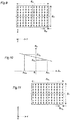
- FIG. 9 is a schematic showing an example of a scanning path of the light beam for scanning within the scanning range of FIG. 8 .
- scanning points irradiated with a pulsed laser beam emitted at regular intervals from the optical scanning device 100 are schematically indicated by black circles.
- a locus of the light beam is indicated by a solid line for convenience of description.
- the mirror part 111 of the two-dimensional scanning mirror 106 when the mirror part 111 of the two-dimensional scanning mirror 106 is rotated around the Y axis, the light beam emitted from the optical scanning device 100 in the X direction moves in the Z-X plane to scan one column vertically (in a main scanning direction) on the plane of the figure.
- the mirror part 111 is rotated around the X axis, the light beam emitted from the optical scanning device 100 in the X direction moves in the X-Y plane, and the scanning path of the light beam moves horizontally (in a sub-scanning direction).
- the frequency of oscillation around the X axis and the frequency of oscillation around the Y axis of the mirror part 111 of the two-dimensional scanning mirror 106 will be denoted by fx and fy, respectively.
- the optical scanning device 100 can scan in the same direction in a period of 1/fx (i.e., the same scanning points in FIG. 9 can periodically be irradiated with the light beam).
- the frequency fx of oscillation around the X axis of the mirror part 111 of the two-dimensional scanning mirror 106 will be referred to as "drive frequency" or "frame rate”.
- the optical scanning device 100 can scan with the light beam and is therefore applicable to a distance measuring device measuring a distance between the optical scanning device 100 and an object therearound and recognizing surrounding conditions. For example, when the vehicle 150 (see FIG. 1 ) runs in the X direction, the optical scanning device 100 can measure a distance in the running direction to check whether an obstacle exists in the running direction.
- a vehicle when a vehicle is accelerated, for example, when a stopped vehicle starts moving, a running speed will increase in the future, so that a distance measuring device mounted on the vehicle is desirably capable of scanning a distant place with high spatial resolution.
- the vehicle when the vehicle is decelerated, for example, when the running vehicle stops, the running speed will decrease in the future, and the running direction of the vehicle is more likely to rapidly change, so that the distance measuring device mounted on the vehicle desirably scans a wide range especially in the horizontal direction.
- the maximum scanning angle ⁇ y has hitherto been changed in accordance with a vehicle acceleration Ax such that the maximum scanning angle ⁇ y is reduced when the acceleration is positive (acceleration) while the maximum scanning angle ⁇ y is increased when the acceleration is negative (deceleration).
- FIG. 10 shows an example of a relationship between the acceleration Ax and the maximum scanning angle ⁇ y when the maximum scanning angle ⁇ y is adjusted in accordance with the acceleration Ax.
- a graph of FIG. 10 shows that the maximum scanning angle ⁇ y is adjusted to ⁇ y 1 at the time of an acceleration Ax 1 (during acceleration) and is adjusted to ⁇ y 2 (> ⁇ y 1 ) at the time of an acceleration Ax 2 (during deceleration).
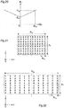
- FIG. 11 is a schematic drawing showing a scanning path and scanning points of a conventional distance measuring device during acceleration (at the time of the acceleration Ax 1 of FIG. 10 ).
- a spatial resolution Ry in this case is Ryi.
- FIG. 12 is a schematic drawing showing a scanning path and scanning points of the conventional distance measuring device during deceleration (at the time of the acceleration Ax 2 of FIG. 10 ).
- the spatial resolution Ry in this case is Ry 2 .
- FIG. 12 showing the case of deceleration
- the scanning points are sparser in the Y direction as compared to FIG. 11 showing the case of acceleration, and the spatial resolution Ry is deteriorated (i.e., Ry1 ⁇ Ry2).
- the prior art has a problem of deterioration in the spatial resolution Ry when the maximum scanning angle ⁇ y is increased.
- the optical scanning device 100 controls the drive frequency (frame rate) fx such that the spatial resolution Ry does not deteriorate even when the maximum scanning angle ⁇ y is changed in accordance with the acceleration Ax of the vehicle 150.
- the drive frequency (frame rate) fx may be controlled such that fx ⁇ ⁇ y is made constant, from Eq. (4), since both Ry and fyc are constants.
- the spatial resolution Ry is kept constant by reducing the drive frequency (frame rate) fx to 1/2.
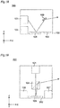
- FIG. 13 is a flowchart showing a method of changing the drive frequency (frame rate) fx in accordance with the acceleration Ax without deteriorating the spatial resolution Ry.
- the drive frequency (frame rate) fx is fx 1
- the drive voltage V is Vy 1
- the maximum scanning angle ⁇ y is ⁇ y 1 .
- the acceleration sensor 105 (see FIGS. 1 and 2 ) of the optical scanning device 100 detects the acceleration Ax in the X direction.
- the controller 103 determines the maximum scanning angle ⁇ y 2 after the change based on the detected acceleration Ax. For example, when the acceleration Ax is negative (during deceleration), the determination is made to satisfy ⁇ y 2 > ⁇ y 1 .
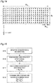
- FIG. 14 is a schematic drawing showing a scanning path and scanning points of the optical scanning device 100 of the first embodiment of the present invention when the drive frequency fx is adjusted in this way.
- the spatial resolution Ry is Ry 1 , which is not change from the spatial resolution during acceleration (see FIG. 11 ).
- the optical scanning device 100 can control the maximum scanning angle ⁇ y of the light beam based on the acceleration Ax and control the drive frequency (frame rate) fx so as to keep the spatial resolution Ry constant even when the maximum scanning angle ⁇ y is changed.
- Another method may be employed to keep the spatial resolution Ry constant. For example, if it is desired to detect a behavior of a specific object in the running direction at a high frame rate, the spatial resolution Ry can be kept constant by controlling the maximum scanning angle ⁇ y based on the target drive frequency (frame rate) fx.
- FIG. 15 is a flowchart showing a method of controlling the maximum scanning angle ⁇ y based on the drive frequency (frame rate) fx without deteriorating the spatial resolution Ry.
- the drive frequency (frame rate) fx is fx 1
- the drive voltage V is Vy 1
- the maximum scanning angle ⁇ y is ⁇ y 1 .
- the acceleration sensor 105 (see FIGS. 1 and 2 ) of the optical scanning device 100 detects the acceleration Ax in the X direction.
- the controller 103 determines the drive frequency (frame rate) fx 2 after the change based on the detected acceleration Ax. For example, as shown in FIG. 16 , when the acceleration Ax is positive (during acceleration), the determination is made to satisfy fx 2 > fx 1 .
- the acceleration sensor 105 and the two-dimensional scanning mirror 106 are formed on the same substrate 102 (see FIGS. 1 and 2 ). Therefore, when attached to a device such as the vehicle 150 (see FIG. 1 ), the optical scanning device 100 has an advantage that it is not necessary to adjust relative positions therebetween.
- the present invention is not limited thereto, and the acceleration sensor 105 and the two-dimensional scanning mirror 106 may be formed on different substrates.
- the drive frequency fx of the oscillation around the X axis is 1/n of the drive frequency fy of the oscillation around the Y axis (see Eq. (2)) and n is an integer.
- n is not limited to an integer. If n is not an integer, the scanning path of the light beam is a so-called Lissajous figure, and the period of irradiation of the same scanning point with the light beam is the reciprocal of the least common multiple of fx and fy, rather than 1/fx. Even in this case, as in the above description, the effect of suppressing the change in the spatial resolution Ry can be obtained by controlling the drive frequency (frame rate) fx.
- the running direction of the vehicle 150 (see FIG. 1 ) is the X-axis direction; however, the present invention is not limited thereto.
- the mirror part 111 of the two-dimensional scanning mirror 106 resonates around the Y axis perpendicular to the running direction (X direction) of the vehicle 150; however, the present invention is not limited thereto, and the mirror part may be resonated and rotationally displaced around another direction.
- the acceleration sensor 105 detects the acceleration in the running direction of the optical scanning device 100; however, the present invention is not limited thereto and, for example, the acceleration sensor may detect the acceleration in the direction orthogonal to the running direction of the optical scanning device 100.
- the acceleration sensor 105 may be capable of detecting the acceleration in directions of two or more axes. As a result, for example, a swing in the Y-axis direction or the Z-axis direction orthogonal to the running direction of the optical scanning device 100 can be detected to adjust the maximum scanning angle in accordance with the magnitude of the swing.
- the frequency fy of the oscillation around the Y axis of the mirror part 111 of the two-dimensional scanning mirror 106 is defined as the specific resonance frequency fyc (see Eq. (1)).
- the first embodiment of the present invention is not limited thereto, and fy may be a frequency near fyc.
- the applied voltage can certainly most efficiently be converted into oscillation when fy is equal to the resonance frequency fyc; however, even when fy is near the resonance frequency fyc, a relatively large amplitude can be obtained at the same applied voltage.
- the maximum scanning angle ⁇ y is uniformly changed ( ⁇ y is expressed as a linear function of Ax) with respect to the change in the acceleration Ax of the optical scanning device 100; however, the first embodiment of the present invention is not limited thereto, and the maximum scanning angle ⁇ y may be determined in accordance with the acceleration Ax.
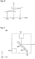
- FIG. 17 is a schematic drawing showing a configuration of an optical scanning device according to a first modification of the first embodiment of the present invention, which is generally denoted by 180.
- a beam splitter is not disposed, and the light beam emitted from the light source 101 enters the two-dimensional scanning mirror 106 without passing through a beam splitter.
- FIG. 18 is a schematic drawing showing a configuration of an optical scanning device according to a second modification of the first embodiment of the present invention, which is generally denoted by 180.
- a beam splitter is not included also in this modification, a fixed mirror 109 reflecting the light beam entering from the two-dimensional scanning mirror 106 is included instead.
- the first embodiment of the present invention can achieve the same effect, so that the freedom of member arrangement can be increased.
- the first modification and the second modification are also applicable to a second embodiment, a third embodiment, and a fourth embodiment of the present invention described later.
- FIG. 19 is a schematic drawing showing a configuration of an optical scanning device according to the second embodiment of the present invention, which is generally denoted by 200.
- 200 an optical scanning device according to the second embodiment of the present invention.
- the same constituent elements as those of the first embodiment are denoted by the same reference numerals and will not be described.
- the optical scanning device 200 includes an angular velocity sensor 207 instead of an acceleration sensor.
- the angular velocity sensor 207 can detect an angular velocity around a vertical axis (Z axis) (hereinafter simply referred to as "angular velocity") ⁇ z.
- the angular velocity sensor 207 is disposed separately from the substrate 202.
- the second embodiment of the present invention is not limited thereto, and the angular velocity sensor 207 may also be formed on the substrate 202 by using a MEMS technique.
- the optical scanning device 200 may be mounted and used on a vehicle (not shown) as in the first embodiment.
- a distance measuring device mounted on the vehicle desirably scans a distant place in the running direction with high spatial resolution.
- the vehicle makes a left or right turn or runs in a curve, it is necessary to widely recognize surrounding conditions, so that the distance measuring device mounted on the vehicle desirably scans a wide range.
- the maximum scanning angle ⁇ y has hitherto been changed in accordance with the angular velocity Qz such that the maximum scanning angle ⁇ y is reduced when the absolute value of the angular velocity ⁇ z is small while the maximum scanning angle ⁇ y is increased when the absolute value of the angular velocity ⁇ z is large.
- FIG. 20 shows an example of a relationship between the angular velocity ⁇ z and the maximum scanning angle ⁇ y when the maximum scanning angle ⁇ y is adjusted in accordance with the angular velocity ⁇ z.
- the angular velocity ⁇ z is zero.
- the angular velocity ⁇ z indicates a positive value.
- FIG. 22 showing the case of turning
- the scanning points are sparser in the Y direction as compared to FIG. 21 showing the case of straight running, and the spatial resolution is deteriorated.
- the prior art has a problem of deterioration in the spatial resolution Ry during turning as compared to during straight running.
- the optical scanning device 200 controls the drive frequency (frame rate) fx such that the spatial resolution Ry does not deteriorate (i.e., fx ⁇ y is made constant, from Eq. (4)) even when the maximum scanning angle ⁇ y is changed in accordance with the angular velocity ⁇ z of the vehicle.
- FIG. 23 is a flowchart showing a method of changing the drive frequency (frame rate) fx in accordance with the angular velocity ⁇ z without deteriorating the spatial resolution Ry.
- the drive frequency (frame rate) fx is fx 1
- the drive voltage V is Vy 1
- the maximum scanning angle ⁇ y is ⁇ y 1 .
- the angular velocity sensor 207 (see FIG. 19 ) of the optical scanning device 200 detects the angular velocity ⁇ z around the Z axis.
- the controller 103 determines the maximum scanning angle ⁇ y 2 after the change based on the detected angular velocity ⁇ z.
- FIG. 24 is a schematic drawing showing a scanning path and scanning points of the optical scanning device 200 according to the second embodiment of the present invention when the drive frequency fx is adjusted in this way.
- the spatial resolution Ry is Ryi, which is not change from the spatial resolution during straight running (see FIG. 21 ).
- the optical scanning device 100 can control the maximum scanning angle ⁇ y of the light beam based on the angular velocity ⁇ z and control the drive frequency (frame rate) fx so as to keep the spatial resolution Ry constant even when the maximum scanning angle ⁇ y is changed.
- the angular velocity sensor 207 detects the angular velocity around the vertical direction of the optical scanning device 200; however, the present invention is not limited thereto and, for example, the angular velocity sensor may detect an angular velocity around an axis orthogonal to the vertical direction.
- the angular velocity sensor 207 may be capable of detecting respective angular velocities around directions of two or more axes.
- the angular velocity sensor 207 may detect rotation of the optical scanning device 200 around an axis in a horizontal plane.
- the maximum scanning angle ⁇ y is uniformly changed with respect to the change in the angular velocity ⁇ z of the optical scanning device 200; however, the second embodiment of the present invention is not limited thereto, and the maximum scanning angle ⁇ y may be determined in accordance with the angular velocity ⁇ z.
- FIG. 25 is a schematic drawing showing a configuration of an optical scanning device according to the third embodiment of the present invention, which is generally denoted by 300.
- 300 the same constituent elements as those of the first or second embodiment are denoted by the same reference numerals and will not be described.
- the light beam emitted from the light source 101 of the optical scanning device 300 is reflected by a two-dimensional scanning mirror 306 disposed on a substrate 302, then reflected by scanning angle conversion means 308, and emitted from the optical scanning device 300.
- the scanning angle conversion means 308 has an inverted truncated cone shape with a central axis defined along the vertical axis (Z axis), and the light beam is reflected by a conical surface 309 of the scanning angle conversion means 308.
- FIG. 26 is a schematic top view of the substrate 302.
- the substrate 302 includes the acceleration sensor 105 for detecting the acceleration of the optical scanning device 300 and the two-dimensional scanning mirror 306 capable of changing a direction of an optical axis of the incident light beam.
- the two-dimensional scanning mirror 306 includes the mirror part 111 and four beams 321 to 324 connected to four points at both ends in the X direction and both ends in the Y direction of the mirror part 111 to support the mirror part 111. Both ends in the X direction and both ends in the Y direction of the mirror part 111 are connected via the respective beams 321 to 324 to the substrate 302. Unlike the first embodiment, the two-dimensional scanning mirror 306 is not provided with a frame (see the frame 113 of FIG. 2 ).
- FIG. 27 is a schematic cross-sectional view of the two-dimensional scanning mirror 306 of the substrate 302 of FIG. 26 as viewed in a direction XXV-XXV.
- the beams 321, 323 (and the beams 322, 324 not shown in FIG. 27 ) are the same as the beams 120 of the first embodiment described with reference to FIG. 3 and are each composed of a beam base 125 that is a portion of the active layer 143, the insulating film 121 formed on the beam base 125, the first electrode 122 formed on the insulating film 121, the piezoelectric film 123 formed on the first electrode 122, and the second electrode 124 formed on the piezoelectric film 123.
- Sine-wave voltages having the same frequency and the same amplitude and different in phase are applied to the piezoelectric film 123 via the first electrode 122 and the second electrode 124 ( FIG. 27 ) of the beams 321 to 324 ( FIG. 26 ).
- a sine-wave voltage V(t) is applied to the piezoelectric film 123 of the beam 321
- a sine-wave voltage V(t- ⁇ /2) having a phase delayed by 90° ( ⁇ /2) from V(t) is applied to the piezoelectric film 123 of the beam 322 while a sine-wave voltage V(t- ⁇ ) having a phase further delayed by 90° is applied to the piezoelectric film 123 of the beam 323 and a sine-wave voltage V(t-3 ⁇ /2) having a phase further delayed by 90° is applied to the piezoelectric film 123 of the beam 324.
- the beams 321 to 324 are displaced in the Z direction depending on the applied voltage, and therefore, when the sine-wave voltages having different phases are respectively applied to the piezoelectric films 123 of the beams 321 to 324 as described above, the mirror part 111 moves such that a normal line of a surface of the mirror part 111 makes a precession movement (precesses) around the center of the mirror part 111. As a result, the normal line at the center of the surface of the mirror part 111 draws an inverted cone with the vertex defined at the center of the surface of the mirror part 111.
- the optical axis of the reflected light beam precesses to draw an inverted cone having the vertex angle of ⁇ as indicated by a broken line of FIG. 25 .
- the mirror part 111 has a mechanical specific resonance frequency foc in terms of the precession. Generally, when a structure is allowed to precess, oscillating the structure at a specific resonance frequency can result in efficient conversion of applied energy into oscillation.
- the light beam reflected by the mirror part 111 of the two-dimensional scanning mirror 306 is subsequently reflected by the conical surface 309 of the scanning angle conversion means 308 and emitted from the optical scanning device 300.
- Eq. (5) a relationship represented by Eq. (5) below is established between an angle ⁇ formed by the horizontal plane (X-Y plane) and the conical surface 309 of the scanning angle conversion means 308 and the vertex angle ⁇ of the inverted cone drawn by the optical axis of the light beam, the optical axis of the light beam emitted from the optical scanning device 300 is on the horizontal plane.
- ⁇ + 2 ⁇ 90 °
- the vertex angle ⁇ of the inverted cone drawn by the optical axis of the light beam can be changed.
- scanning can be performed such that the optical axis of the light beam emitted from the optical scanning device 300 moves upward and downward from the horizontal plane.
- the optical scanning device 300 of the third embodiment can advantageously scan the entire circumference in the horizontal direction.
- FIG. 29 is a schematic drawing showing a vehicle 350 equipped with the optical scanning device 300.
- the optical scanning device 300 can scan the entire circumference in the horizontal direction and therefore can advantageously be applied to a distance measuring device mounted on the vehicle 350 and recognizing the surrounding conditions.
- FIG. 30 is a schematic drawing showing an example of a scanning path of a light beam for scanning within a scanning range by the optical scanning device 300 of the third embodiment.
- scanning points irradiated with a pulsed laser beam emitted at regular intervals from the optical scanning device 100 are schematically indicated by black circles.
- a locus of the light beam is indicated by a solid line for convenience of description.
- the controller 103 applies a sine-wave drive voltage V to each of the piezoelectric films 123 of the beams 321 to 324 (see FIG. 27 ) such that the mirror part 111 of the two-dimensional scanning mirror 306 precesses at the specific resonance frequency foc.
- the maximum amplitude V A of the drive voltage V is controlled to increase and decrease at a frequency fr (hereinafter, this frequency is referred to as "amplitude change frequency" or "frame rate"). Since the optical scanning device 300 can scan the entire circumference in the horizontal direction, the maximum scanning angle in the horizontal direction is 360°. The matrix of the scanning points of FIG. 30 is obtained in this way.
- the maximum scanning angle ⁇ z is changed by changing the maximum amplitude VA of the drive voltage V in accordance with the acceleration Ax in the running direction of the vehicle 350 (see FIG. 29 ).
- the maximum scanning angle ⁇ z is increased from ⁇ z 1 of FIG. 30 to ⁇ z 2 (> ⁇ z1) and the amplitude change frequency fr is not changed, the scanning path of the light beam is as shown in FIG. 31 .
- the scanning points are sparser in the Z direction as compared to FIG. 30 showing the case of the smaller maximum scanning angle ⁇ z, and a spatial resolution Rz is deteriorated (a spatial resolution Rz 2 of FIG. 30 is deteriorated as compared to a spatial resolution Rz 1 of FIG. 30 ).
- the optical scanning device 300 controls the amplitude change frequency (frame rate) fr by using Eq. (6) below such that the spatial resolution Ry does not deteriorate even when the maximum scanning angle ⁇ z is changed in accordance with the acceleration Ax of the vehicle 350.
- fr ⁇ ⁇ z / Rz foc
- fr When it is desired to keep the spatial resolution Rz constant, fr may be controlled such that fx ⁇ y is made constant, from Eq. (6), since both Rz and foe are constants.
- FIG. 32 is a flowchart showing a method of changing the amplitude change frequency (frame rate) fr in accordance with the acceleration Ax without deteriorating the spatial resolution Rz.
- the amplitude change frequency (frame rate) fr is fr 1
- the amplitude change amount ⁇ V A is ⁇ V A1
- the maximum scanning angle ⁇ z is ⁇ z 1 .
- the acceleration sensor 105 see FIG. 25
- the optical scanning device 300 detects the acceleration Ax in the X direction.
- the controller 103 determines the maximum scanning angle ⁇ z 2 after the change based on the detected acceleration Ax.
- FIG. 33 is a schematic drawing showing a scanning path and scanning points of the optical scanning device 300 of the third embodiment of the present invention when fr of the amplitude change is adjusted in this way.
- the spatial resolution Rz is Rzi, which is not change from the spatial resolution before the change (see FIG. 30 ).
- the optical scanning device 300 includes the acceleration sensor 105; however, the optical scanning device 300 according to the third embodiment of the present invention may include the angular velocity sensor described in the second embodiment and may determine the maximum scanning angle ⁇ z and the amplitude change frequency (frame rate) fr based on the angular velocity.
- the optical scanning device 300 can control the maximum scanning angle ⁇ z of the light beam based on the acceleration or angular velocity and control the drive frequency (frame rate) fr so as to keep the spatial resolution Rz constant even when the maximum scanning angle ⁇ z is changed.
- FIG. 34 is a schematic drawing showing a configuration of an optical scanning device according to the fourth embodiment of the present invention, which is generally denoted by 400.
- 400 an optical scanning device according to the fourth embodiment of the present invention.
- the same constituent elements as those of the second or third embodiment are denoted by the same reference numerals and will not be described.
- the optical scanning device 400 includes a controller 403 controlling the attitude of the two-dimensional scanning mirror 106 based on a velocity.
- the controller 403 derives a velocity vx in the X direction by integrating the acceleration Ax in the X direction detected by the acceleration sensor 105.
- the optical scanning device 400 may be mounted and used on a vehicle (not shown) as in the first embodiment.
- a distance measuring device mounted on the vehicle desirably scans a distant place with high spatial resolution.
- the vehicle runs at a low velocity for example, when the vehicle runs slowly, the running direction of the vehicle is more likely to rapidly change due to left or right turn etc., so that the distance measuring device mounted on the vehicle desirably scans a wide range especially in the horizontal direction.
- the maximum scanning angle ⁇ y has hitherto been changed in accordance with the velocity vx of the vehicle such that the maximum scanning angle ⁇ y is reduced in the case of a high velocity while the maximum scanning angle ⁇ y is increased in the case of a low velocity.
- FIG. 35 shows an example of a relationship between the velocity vx and the maximum scanning angle ⁇ y when the maximum scanning angle ⁇ y is adjusted in accordance with the velocity vx.
- a graph of FIG. 35 shows that the maximum scanning angle ⁇ y is adjusted to ⁇ y 1 at the time of a velocity vx 1 (at high velocity) and is adjusted to ⁇ y 2 (> ⁇ y 1 ) at the time of a velocity vx 2 (at low velocity, vx 2 ⁇ vx 1 ).
- the scanning path and the scanning points at high velocity are the same as those of FIG. 11 of the first embodiment.
- the scanning path and the scanning points of the conventional distance measuring device at low velocity are the same as those of FIG. 12 .
- the spatial resolution at low velocity is deteriorated as compared to the spatial resolution at high velocity.
- the optical scanning device 400 controls the drive frequency (frame rate) fx such that the spatial resolution Ry does not deteriorate even when the maximum scanning angle ⁇ y is changed in accordance with the velocity vx of the vehicle.
- FIG. 36 is a flowchart showing a method of changing the drive frequency (frame rate) fx in accordance with the velocity vx without deteriorating the spatial resolution Ry.
- the drive frequency (frame rate) fx is fx 1
- the drive voltage V is Vy 1
- the maximum scanning angle ⁇ y is ⁇ y 1 .
- the acceleration sensor of the optical scanning device 400 detects the acceleration Ax in the X direction.
- the velocity vx in the X-axis direction is calculated through time integration of Ax.
- the controller 403 determines the maximum scanning angle ⁇ y 2 after the change based on the calculated velocity vx.
- the controller 403 calculates the velocity through time integration of the acceleration Ax detected by the acceleration sensor; however, the present invention is not limited thereto as long as velocity information can be obtained.
- the optical scanning device 400 may include a velocity sensor not shown, and the velocity may be detected by the velocity sensor.
- the velocity sensor may obtain the velocity information from the number of rotations of an axle, for example.
- the optical scanning device 400 can control the maximum scanning angle ⁇ y of the light beam based on the velocity vx and control the drive frequency (frame rate) fx so as to keep the spatial resolution Ry constant even when the maximum scanning angle ⁇ y is changed.
- the maximum scanning angle ⁇ y is uniformly changed with respect to the change in the velocity vx of the optical scanning device 400; however, the fourth embodiment of the present invention is not limited thereto, and the maximum scanning angle ⁇ y may be determined in accordance with the velocity vx.
Applications Claiming Priority (2)
| Application Number | Priority Date | Filing Date | Title |
|---|---|---|---|
| JP2018045774 | 2018-03-13 | ||
| PCT/JP2018/046305 WO2019176204A1 (fr) | 2018-03-13 | 2018-12-17 | Dispositif de balayage optique et son procédé de commande |
Publications (2)
| Publication Number | Publication Date |
|---|---|
| EP3767367A1 true EP3767367A1 (fr) | 2021-01-20 |
| EP3767367A4 EP3767367A4 (fr) | 2021-05-12 |
Family
ID=67906663
Family Applications (1)
| Application Number | Title | Priority Date | Filing Date |
|---|---|---|---|
| EP18909458.4A Withdrawn EP3767367A4 (fr) | 2018-03-13 | 2018-12-17 | Dispositif de balayage optique et son procédé de commande |
Country Status (5)
| Country | Link |
|---|---|
| US (1) | US20210011282A1 (fr) |
| EP (1) | EP3767367A4 (fr) |
| JP (1) | JP6789438B2 (fr) |
| CN (1) | CN111819486A (fr) |
| WO (1) | WO2019176204A1 (fr) |
Cited By (1)
| Publication number | Priority date | Publication date | Assignee | Title |
|---|---|---|---|---|
| EP4254042A1 (fr) * | 2022-03-28 | 2023-10-04 | FUJIFILM Corporation | Dispositif de balayage optique, procédé de commande de dispositif de balayage optique et dispositif de mesure de distance |
Families Citing this family (5)
| Publication number | Priority date | Publication date | Assignee | Title |
|---|---|---|---|---|
| JP6827601B1 (ja) * | 2020-02-19 | 2021-02-10 | 三菱電機株式会社 | 光反射装置およびそれを備えた測距装置 |
| JP6833127B1 (ja) * | 2020-03-26 | 2021-02-24 | 三菱電機株式会社 | 光走査装置、光走査装置の制御方法、及び測距装置 |
| CN111508383B (zh) * | 2020-04-23 | 2022-03-25 | 歌尔光学科技有限公司 | 成像方法、成像装置及计算机可读存储介质 |
| CN113687387B (zh) * | 2021-09-07 | 2024-03-01 | 广州大学 | 一种激光雷达扫描装置以及激光雷达扫描方法 |
| WO2023053840A1 (fr) * | 2021-09-28 | 2023-04-06 | 富士フイルム株式会社 | Dispositif de balayage optique |
Family Cites Families (18)
| Publication number | Priority date | Publication date | Assignee | Title |
|---|---|---|---|---|
| JPH11153664A (ja) * | 1997-09-30 | 1999-06-08 | Sumitomo Electric Ind Ltd | 繰り返しパルス光を利用した物体検知装置 |
| JP2000075030A (ja) * | 1998-08-27 | 2000-03-14 | Aisin Seiki Co Ltd | スキャン型レーザーレーダ装置 |
| US7732751B2 (en) * | 2005-06-13 | 2010-06-08 | Arete' Associates | Optical systems and methods using microelectromechanical-systems mirrors exceeding thirty microns |
| US7262895B2 (en) * | 2005-06-14 | 2007-08-28 | Lexmark International, Inc. | Determining operating point of feedback controller applied to operation of oscillating scanning device |
| US8050863B2 (en) * | 2006-03-16 | 2011-11-01 | Gray & Company, Inc. | Navigation and control system for autonomous vehicles |
| JP4881073B2 (ja) * | 2006-05-30 | 2012-02-22 | キヤノン株式会社 | 光偏向器、及びそれを用いた光学機器 |
| JP5304380B2 (ja) * | 2008-07-23 | 2013-10-02 | 株式会社リコー | 光走査装置、これを用いた画像投影装置、ヘッドアップディスプレイ装置および携帯電話機 |
| DE102008055159A1 (de) * | 2008-12-29 | 2010-07-01 | Robert Bosch Gmbh | Adaptive Winkel- und Leistungsanpassung bei 3D-Mikrospiegel-Lidar |
| JP4620789B1 (ja) * | 2009-07-16 | 2011-01-26 | シナノケンシ株式会社 | 光走査装置 |
| EP2339367A1 (fr) * | 2009-12-17 | 2011-06-29 | Siemens Aktiengesellschaft | Appareil à balayage laser |
| JP6234781B2 (ja) * | 2013-11-07 | 2017-11-22 | リコー光学株式会社 | 2次元走査型レーザビーム放射装置 |
| WO2015108710A1 (fr) * | 2014-01-20 | 2015-07-23 | Apple Inc. | Détection de position de miroir utilisant la frange de distorsion de champs électriques |
| JP6417833B2 (ja) * | 2014-10-01 | 2018-11-07 | 富士通株式会社 | レーザ測距装置、プログラム及びレーザ測距装置の補正方法 |
| JP6536008B2 (ja) | 2014-10-30 | 2019-07-03 | 株式会社デンソー | 車両用光飛行型測距装置 |
| US9625582B2 (en) * | 2015-03-25 | 2017-04-18 | Google Inc. | Vehicle with multiple light detection and ranging devices (LIDARs) |
| DE102015109160A1 (de) * | 2015-06-10 | 2016-12-15 | Valeo Schalter Und Sensoren Gmbh | Fahrerassistenzsystem für ein Kraftfahrzeug, Kraftfahrzeug sowie Verfahren |
| US10761195B2 (en) * | 2016-04-22 | 2020-09-01 | OPSYS Tech Ltd. | Multi-wavelength LIDAR system |
| KR101877388B1 (ko) * | 2016-07-21 | 2018-07-11 | 엘지전자 주식회사 | 차량용 라이다 장치 |
-
2018
- 2018-12-17 CN CN201880090386.6A patent/CN111819486A/zh active Pending
- 2018-12-17 EP EP18909458.4A patent/EP3767367A4/fr not_active Withdrawn
- 2018-12-17 US US16/964,402 patent/US20210011282A1/en not_active Abandoned
- 2018-12-17 WO PCT/JP2018/046305 patent/WO2019176204A1/fr unknown
- 2018-12-17 JP JP2020505593A patent/JP6789438B2/ja active Active
Cited By (1)
| Publication number | Priority date | Publication date | Assignee | Title |
|---|---|---|---|---|
| EP4254042A1 (fr) * | 2022-03-28 | 2023-10-04 | FUJIFILM Corporation | Dispositif de balayage optique, procédé de commande de dispositif de balayage optique et dispositif de mesure de distance |
Also Published As
| Publication number | Publication date |
|---|---|
| US20210011282A1 (en) | 2021-01-14 |
| CN111819486A (zh) | 2020-10-23 |
| EP3767367A4 (fr) | 2021-05-12 |
| JP6789438B2 (ja) | 2020-11-25 |
| WO2019176204A1 (fr) | 2019-09-19 |
| JPWO2019176204A1 (ja) | 2020-10-08 |
Similar Documents
| Publication | Publication Date | Title |
|---|---|---|
| EP3767367A1 (fr) | Dispositif de balayage optique et son procédé de commande | |
| US11656539B2 (en) | Microelectromechanical device with a structure tiltable by piezoelectric actuation having improved mechanical and electrical characteristics | |
| US9864187B2 (en) | Micromechanical structure with biaxial actuation and corresponding MEMS device | |
| US6595055B1 (en) | Micromechanical component comprising an oscillating body | |
| US10330922B2 (en) | Biaxial optical deflector including multiple mirror units, laser radar system, and manufacturing method | |
| EP3287830B1 (fr) | Système réflecteur mems de balayage | |
| EP3447560B1 (fr) | Système réflecteur mems | |
| JP6278130B2 (ja) | 微小光学電気機械デバイスおよびその製造方法 | |
| US20170285332A1 (en) | Mems device oscillating about two axes and having a position detecting system, in particular of a piezoresistive type | |
| US20180157030A1 (en) | Electrostatically actuated oscillating structure with oscillation starting phase control, and manufacturing and driving method thereof | |
| US20140240810A1 (en) | MEMS Drive and Beam-Steering Apparatus | |
| US20160062109A1 (en) | Optical scanning device | |
| US9436000B2 (en) | Optical deflector including meander-type piezoelectric actuators and ill-balanced mirror structure | |
| EP3839602A1 (fr) | Dispositif de miroir microelectromecanique avec actionnement piezoélectrique, ayant une structure améliorée | |
| EP3636588B1 (fr) | Ressorts à réglage de fréquence mems | |
| EP3640705B1 (fr) | Dispositif de balayage optique, son procédé de commande, et corps mobile | |
| US20230139572A1 (en) | Optical scanning device and method of driving micromirror device | |
| EP2844611B1 (fr) | Dispositif mems | |
| EP4242724A1 (fr) | Dispositif de miroir microélectromécanique biaxial à actionnement piézoélectrique | |
| EP4082962A1 (fr) | Dispositif de miroir microélectromécanique à actionnement piézo-électrique et angle d'ouverture amélioré | |
| EP4286916A1 (fr) | Dispositif de balayage optique et procédé d'entraînement d'un dispositif à micromiroir | |
| US20230003996A1 (en) | Mems device and method of driving mems device | |
| WO2020194691A1 (fr) | Dispositif de balayage optique et son procédé de commande | |
| JP2006136084A (ja) | 揺動体装置、及びその作製方法 | |
| JP2022032538A (ja) | 光偏向装置、光走査装置及び光走査式測距装置 |
Legal Events
| Date | Code | Title | Description |
|---|---|---|---|
| STAA | Information on the status of an ep patent application or granted ep patent |
Free format text: STATUS: THE INTERNATIONAL PUBLICATION HAS BEEN MADE |
|
| PUAI | Public reference made under article 153(3) epc to a published international application that has entered the european phase |
Free format text: ORIGINAL CODE: 0009012 |
|
| STAA | Information on the status of an ep patent application or granted ep patent |
Free format text: STATUS: REQUEST FOR EXAMINATION WAS MADE |
|
| 17P | Request for examination filed |
Effective date: 20200907 |
|
| AK | Designated contracting states |
Kind code of ref document: A1 Designated state(s): AL AT BE BG CH CY CZ DE DK EE ES FI FR GB GR HR HU IE IS IT LI LT LU LV MC MK MT NL NO PL PT RO RS SE SI SK SM TR |
|
| AX | Request for extension of the european patent |
Extension state: BA ME |
|
| A4 | Supplementary search report drawn up and despatched |
Effective date: 20210413 |
|
| RIC1 | Information provided on ipc code assigned before grant |
Ipc: B81B 7/04 20060101ALI20210407BHEP Ipc: G02B 26/10 20060101AFI20210407BHEP Ipc: B81B 3/00 20060101ALI20210407BHEP Ipc: G01S 7/481 20060101ALI20210407BHEP Ipc: G01S 17/93 20200101ALI20210407BHEP Ipc: G02B 26/08 20060101ALI20210407BHEP Ipc: G01S 17/931 20200101ALI20210407BHEP |
|
| DAV | Request for validation of the european patent (deleted) | ||
| DAX | Request for extension of the european patent (deleted) | ||
| STAA | Information on the status of an ep patent application or granted ep patent |
Free format text: STATUS: EXAMINATION IS IN PROGRESS |
|
| 17Q | First examination report despatched |
Effective date: 20211203 |
|
| STAA | Information on the status of an ep patent application or granted ep patent |
Free format text: STATUS: THE APPLICATION HAS BEEN WITHDRAWN |
|
| 18W | Application withdrawn |
Effective date: 20220324 |