WO2019167100A1 - 半導体単結晶インゴットのスライス方法 - Google Patents
半導体単結晶インゴットのスライス方法 Download PDFInfo
- Publication number
- WO2019167100A1 WO2019167100A1 PCT/JP2018/007074 JP2018007074W WO2019167100A1 WO 2019167100 A1 WO2019167100 A1 WO 2019167100A1 JP 2018007074 W JP2018007074 W JP 2018007074W WO 2019167100 A1 WO2019167100 A1 WO 2019167100A1
- Authority
- WO
- WIPO (PCT)
- Prior art keywords
- ingot
- single crystal
- slicing
- wafer
- rotation angle
- Prior art date
- Legal status (The legal status is an assumption and is not a legal conclusion. Google has not performed a legal analysis and makes no representation as to the accuracy of the status listed.)
- Ceased
Links
Images








Classifications
-
- B—PERFORMING OPERATIONS; TRANSPORTING
- B28—WORKING CEMENT, CLAY, OR STONE
- B28D—WORKING STONE OR STONE-LIKE MATERIALS
- B28D5/00—Fine working of gems, jewels, crystals, e.g. of semiconductor material; apparatus or devices therefor
- B28D5/04—Fine working of gems, jewels, crystals, e.g. of semiconductor material; apparatus or devices therefor by tools other than rotary type, e.g. reciprocating tools
-
- H—ELECTRICITY
- H10—SEMICONDUCTOR DEVICES; ELECTRIC SOLID-STATE DEVICES NOT OTHERWISE PROVIDED FOR
- H10P—GENERIC PROCESSES OR APPARATUS FOR THE MANUFACTURE OR TREATMENT OF DEVICES COVERED BY CLASS H10
- H10P52/00—Grinding, lapping or polishing of wafers, substrates or parts of devices
Definitions
- the present invention relates to a method for manufacturing a semiconductor single crystal wafer such as a silicon single crystal wafer by slicing a semiconductor single crystal ingot such as a silicon single crystal ingot.
- the single crystal member is moved along a predetermined cutting surface.
- the cutting direction of the machining tool is set in a direction inclined to the direction in which the chips of the single crystal member are discharged by the cutting tool with respect to the normal direction perpendicular to the intersecting line between the planned cutting plane and the cleavage plane.
- a single crystal cutting method is disclosed in which the inclination angle from the normal direction of the cutting direction is set to an angle at which the cutting efficiency of the single crystal member by the processing tool is maximized (see, for example, Patent Document 1).
- the cleavage plane of the single crystal member appears as intersecting lines A and B on the planned cutting plane.
- the cutting direction in which the cutting efficiency is maximized is the rotation angle ⁇ 1 from the normal line P, Q perpendicular to each of the intersecting lines A, B to the chip discharging direction side, either clockwise or counterclockwise.
- the directions are Z 1 , Z 2 , Z 3 , Z 4 , Z 5 , Z 6 , Z 7 , Z 8 inclined by ⁇ 2 , ⁇ 3 , ⁇ 4 , ⁇ 5 , ⁇ 6 , ⁇ 7 , ⁇ 8, respectively. .
- ⁇ 1 is 24 degrees
- ⁇ 2 is 7 degrees
- ⁇ 3 is 16 degrees
- ⁇ 4 is 8 degrees
- ⁇ 5 is 20 degrees
- ⁇ 6 is 17 degrees
- ⁇ 7 is 16 degrees
- ⁇ 8 is 5 degrees.
- the chips of the single crystal member are discharged with respect to the normal line that is on the planned cut surface of the single crystal and perpendicular to the intersecting line between the planned cut surface and the cleavage plane. From the direction in which the cutting ability determined by the crystallographic characteristics of the single crystal member having the positive rotation angle and the pressure contact force between the single crystal member and the processing tool is maximized. Since the single crystal member is cut by giving a cut, the cutting and removing efficiency is improved at each stage, and the cutting processing time that has been spent for a long time can be shortened. Further, since the single crystal member is not excessively strained during processing, the cut wafer is prevented from being bent or warped.
- the single crystal ingot is sliced along the planned cutting plane, and the crystal orientation of the single crystal ingot is set to ⁇ 111>, and a single crystal cutting method of slicing parallel to the direction of the crystal habit line is disclosed (for example, see Patent Document 2).
- the crystal orientation of the single crystal ingot is determined in advance to ⁇ 111>, and the cutting direction of the cutting machine is matched with the crystal habit line direction of the single crystal ingot. Since the single crystal ingot is sliced in parallel with the direction of the crystal habit line by a machine, a wafer with very little bending or warping can be cut and separated, and the cutting efficiency can be remarkably improved. That is, the cleavage plane of the macro single crystal ingot is usually the (111) plane, and the slice direction of the single crystal ingot was corrected along the crystal habit line generated by the difference in the degree of crystal plane development, and thus was cut. An ideal wafer is obtained in which bending and warping are hardly generated on the wafer.
- a cylindrical semiconductor single crystal ingot is bonded and held by a holder in a state of being rotated by a predetermined rotation angle around the crystal axis of the ingot different from the central axis of the cylinder of the ingot, and in this state, the In the semiconductor single crystal ingot slicing method in which the ingot is sliced by a cutting device, a predetermined rotation angle is determined when the ingot is bonded and held by a holder so that the warpage amount of the wafer sliced by the cutting device becomes a predetermined amount.
- a method for slicing a semiconductor single crystal ingot is disclosed (for example, see Patent Document 3).
- the cylindrical semiconductor single crystal ingot must be cut in accordance with the crystal axis of the ingot different from the central axis of the cylinder of the ingot.
- the rotation angle of the ingot is limited, the setting range of the predetermined rotation angle when the ingot is bonded and held by the holder is set wide, and the angle for adjusting the deviation of the crystal axis of the ingot is the predetermined rotation
- the predetermined rotation angle needs to be set wide so that the angle is within the range, and as a result, the amount of warpage of the wafer may increase.
- An object of the present invention is to provide a method for slicing a semiconductor single crystal ingot that not only can reduce the amount of warpage of a wafer but also can accurately control the amount of warpage of the wafer to a desired amount.
- a cylindrical semiconductor single crystal ingot is bonded and held by a holder while being rotated by a predetermined rotation angle about a crystal axis of an ingot different from the central axis of the cylinder of the ingot.
- the predetermined amount when the ingot is bonded and held by the holder so that the warpage amount of the wafer sliced by the cutting device becomes a predetermined amount.
- a tilt angle of the holder by the cutting device is determined.
- the ingot is centered on the crystal axis of the ingot different from the central axis of the cylinder. Then, the ingot is bonded and held by the holding tool in a state where the ingot is rotated by a predetermined rotation angle around the crystal axis. At this time, since the predetermined rotation angle around the crystal axis and the tilt angle of the holder by the cutting device were determined so that the warpage amount of the wafer sliced by the cutting device was a predetermined amount, the ingot was The amount of warping of the wafer after slicing can be accurately controlled to a desired amount.
- a second aspect of the present invention is an invention based on the first aspect, and further obtains a correlation with respect to a change in the amount of warpage of the wafer with respect to a change in the predetermined rotation angle in advance by experiment, and calculates the predetermined rotation angle. It is characterized by determining from this correlation.
- the correlation between the change in the amount of warpage of the wafer with respect to the change in the predetermined rotation angle is obtained in advance by experiment, and the predetermined rotation angle is determined from this correlation.
- the amount of warping of the wafer after slicing can be controlled with a desired amount with high accuracy.
- a third aspect of the present invention is an invention based on the first aspect, and further includes a predetermined time when the ingot is bonded and held by a holder so that the amount of warpage of the wafer sliced by the cutting device is minimized.
- the rotation angle is determined.
- the predetermined rotation angle around the crystal axis of the ingot is determined so that the amount of warpage of the wafer sliced by the cutting device is minimized, the ingot is sliced. The amount of warpage of the subsequent wafer can be reduced.
- a fourth aspect of the present invention is the invention based on the first aspect, wherein the rotation reference portion is further formed in the ingot, and when the perpendicular line drawn from the crystal axis of the ingot to the rotation reference portion is used as the reference line,
- the predetermined rotation angle with respect to the reference line is within a range of 45 to 55 degrees, 125 to 135 degrees, 225 to 235 degrees, and 305 to 315 degrees.
- a perpendicular drawn from the crystal axis of the ingot to the rotation reference portion is used as a reference line, and predetermined rotation angles with respect to this reference line are 45 to 55 degrees, 125 to 135 degrees, 225 to By setting it within the range of 235 degrees and any of 305 to 315 degrees, the warpage amount of the wafer after cutting the ingot becomes almost a desired amount.
- a perspective view (a) of the wafer showing a mechanism in which the cleavage plane appears in the cutting direction during the cutting of the ingot by the wire and the wire is displaced in the direction of the cleavage plane, and a side view (b) of the wafer after cutting in which a large warp has occurred.
- a perspective view (a) of a wafer showing a mechanism in which a cleavage plane does not appear in the cutting direction during the cutting of the ingot by the wire and the wire advances straight in the cutting direction, and a side view (b) of the wafer after cutting without warping It is. It is a front view of an ingot which shows that the cleavage surface of an ingot is parallel to the wire mark of the ingot surface.
- It is a block diagram of the ingot which shows the state where the center axis
- a wire saw device 16 is used to slice and cut the silicon single crystal ingot 13.
- a wire saw device 16 as a cutting device is provided below the first and second main rollers 11 and 12, and the first and second main rollers 11 and 12 disposed in the same horizontal plane with the central axes parallel to each other.
- the single sub-roller 17 provided at an intermediate position between the first and second main rollers 11 and 12 and the first and second main rollers 11 and 12 and the single sub-roller 17 are wound around and stretched.
- a lifting device 19 that lifts and lowers the holding tool 14 (FIGS. 1 and 2).
- the outer peripheral surfaces of the first and second main rollers 11 and 12 and the single sub-roller 17 are spaced at predetermined intervals in the axial direction of the rollers 11, 12 and 17, that is, the thickness of the wafer to be sliced.
- a plurality of ring grooves (not shown) extending in the circumferential direction are formed at intervals in the axial direction of the rollers 11, 12, and 17.
- the wire 18 is one long piece wound around the feeding bobbin 21 (FIG. 2), and the wire 18 fed from the feeding bobbin 21 is connected to the first and second main rollers 11 and 12 in a single manner.
- the rollers 11, 12, and 17 are spirally wound around the rollers 11, 12, and 17 so as to be sequentially accommodated from the ring grooves on one end side to the ring grooves on the other end side of the sub-roller 17. After being stretched, it is configured to be wound on a winding bobbin 22 (FIG. 2).
- the holder 14 includes a slicing base 14a bonded to the ingot 13 and a work plate 14b that holds the slicing base 14a.
- the slicing base 14a is formed of the same material as the ingot 13, or glass, ceramic, carbon, resin, or the like, but carbon, resin, or the like is often used in consideration of cost and ease of molding.
- the adhesive epoxy resin, thermoplastic wax or the like is used, and the work plate 14b is mainly formed of SUS.
- the lifting device 19 includes a support member 19a provided so as to extend in the vertical direction, and a horizontal member 19b attached to the support member 19a so as to be lifted and lowered and holding the holding tool 14 on the lower surface of the tip.
- the ingot 13 bonded to the holder 14 is configured to be movable up and down by the lifting device 19.
- the crystal orientation of the ingot 13 varies somewhat, and does not necessarily coincide with the central axis of the cylinder of the ingot 13. Therefore, when the slicing base 14a is bonded in accordance with the direction of the central axis of the cylinder of the ingot 13 and attached to the wire saw device 16 for slicing, the cut surface of the wafer cut out from the ingot 13 does not coincide with the crystal lattice plane. This causes a problem that the characteristics of the wafer vary. As one method for solving this problem, a method using a gonio angle setting device 19c is known.
- the gonio angle setting device 19 c is attached to the lower surface of the horizontal member 19 b, and can adjust the attachment angle of the holding tool 14 attached to the wire saw device 16 in a plane orthogonal to the wire 18.
- the gonio angle setting device 19c includes a fixed member 191 and a movable member 192, as shown in FIG.
- the fixing member 191 is attached to the horizontal member 19b.
- the lower surface of the fixing member 191 is a concave curved surface, and the concave curved surface is a cylindrical concave curved surface having an arc-shaped cross section in a plane orthogonal to the traveling direction of the wire 18.
- a movable member 192 is attached to the lower surface of the fixed member 191.
- the movable member 192 has a convex curved surface that follows the concave curved surface formed on the lower surface of the fixed member 191 on the upper surface, and when the movable member 192 is moved relative to the fixed member 191, a surface orthogonal to the traveling direction of the wire 18.
- the movable member 192 can be adjusted in the vertical direction.
- the vertical shaft 193 is rotated to change the screwing position of the feed screw formed at the center.
- the movable member 192 moves along the curved surface of the fixed member 191 in a plane orthogonal to the wire 18, and the vertical position adjustment is possible.
- the traveling direction of the wire 18 can be adjusted so that the crystal orientation of the ingot 13 is in an appropriate direction within a plane orthogonal to the wire 18.
- a method of slicing the silicon single crystal ingot 13 using the wire saw device 16 configured as described above will be described.
- the wire 18 is wound and stretched between the first and second main rollers 11 and 12 and the single sub-roller 17.
- the wires 18 that are horizontally stretched between the first and second main rollers 11 and 12 become horizontal due to the rotation of the first and second main rollers 11 and 12 and the single sub-roller 17.
- the work plate 14b to which the ingot 13 and the slicing base 14a are bonded is mounted on a gonio angle setting device 19c provided on the lower surface of the front end of the horizontal member 19b of the lifting device 19 by fixing means such as bolting.
- a predetermined rotation angle is rotated around the center axis of the cylinder of the ingot 13 and bonded.
- the predetermined rotation angle is determined so that the warpage amount of the wafer 23 obtained by slicing by the wire saw device 16 becomes a predetermined amount.
- a perpendicular line extending from the crystal axis 13b of the ingot 13 to the orientation flat 13c is defined as a reference line 13d, and predetermined rotation angles ⁇ (FIGS. 5 and 6) with respect to the reference line 13d are 45 to 55 degrees, 125 to 135 degrees, It is preferably set within the range of 225 to 235 degrees and 305 to 315 degrees.
- the predetermined rotation angle ⁇ with respect to the reference line 13d is within a range of 45 to 55 degrees or 305 to 315 degrees in order to avoid the orientation flat 13c. It is preferable to set to.
- the reason why the predetermined rotation angle ⁇ with respect to the reference line 13d is limited to the above range is that the wire 18 is likely to be displaced in the direction of the cleavage surface 13e of the ingot 13, and the wafer obtained by slicing the ingot 13 This is because the variation in the amount of warpage of 23 increases.
- FIG. 9A the central axis 13a of the cylinder coincides with the crystal axis 13b, and the central axis 13a of the cylinder. Is almost the same as the crystal axis 13b (FIG. 4 (P1-P2), FIG. 9B).
- the inclination angle between the central axis 13a of the cylinder of the ingot 13 and the crystal axis 13b of the ingot 13 is about 3 degrees at the maximum.
- the surface of the sliced wafer 23 is required to be a plane perpendicular to the crystal axis 13b of the ingot 13 (FIG. 9C).
- the crystal axis 13b of the ingot 13 is displaced from the longitudinal direction of the slice table 14a.
- the horizontal direction (XZ plane in FIG. 4) corrects the bonding direction between the slicing base 14a and the work plate 14b, and bonds the crystal axis 13b of the ingot 13 within the YZ plane in FIG.
- the ingot 13 passes through the central axes of the first and second main rollers 11 and 12 above the wire 18 horizontally stretched between the first and second main rollers 11 and 12.
- the crystal axis 13b of the ingot 13 is moved between the vertical lines so as to be substantially parallel to the central axes of the first and second main rollers 11 and 12 (FIGS. 1 and 2).
- the vertical plane including the crystal axis 13b of the ingot 13 is orthogonal to the extending direction of the wire 18 between the first and second main rollers 11 and 12 (FIG. 9C).
- the fixing angle of the holder 14 is adjusted by the gonio angle setting device 19c for fixing the holder 14 so that the crystal axis 13b is parallel to the central axes of the first and second main rollers 11 and 12.
- the crystal axis 13b of the ingot 13 is orthogonal to a plane formed by the wire 18 between the first and second main rollers 11 and 12 and the cutting direction of the ingot 13 by the wire 18.
- the ingot 13 is lowered in the vertical direction and moved to a position crossing the wire 18 moving in the horizontal direction, thereby slicing the ingot 13.
- the curvature amount of the wafer 23 after slicing the ingot 13 can be accurately controlled to a desired amount.
- the warpage amount of the wafer 23 obtained by slicing the ingot 13 may be different.
- FIGS. 7A and 8A even if the cleavage plane 13e of the ingot 13 is parallel to the wire mark 13f on the surface of the ingot 13, the cleavage plane 13e of the ingot 13 is a crystal of the ingot 13 as shown in FIG. 7B. There is a case where it is inclined with respect to the axis 13b and a case where it is parallel to the crystal axis 13b of the ingot 13 as shown in FIG. 8B.
- the cleavage plane 13e of the ingot 13 is parallel to the wire mark 13f on the surface of the ingot 13 (FIG. 7A)
- the cleavage plane 13e of the ingot 13 is relative to the crystal axis 13b of the ingot 13 as shown in FIG. 7B. If it is inclined, the wafer 23 obtained by slicing the ingot 13 warps as shown in the side view (b) of FIG.
- the cleavage plane 13e of the ingot 13 has a crystal axis 13b of the ingot 13 as shown in FIG.
- the wafer 23 obtained by slicing the ingot 13 does not warp as shown in the side view (b) of FIG. Even if the cleaved surface 13e of the ingot 13 is not parallel to the crystal axis 13b of the ingot 13 as shown in FIG. 8B, the wafer 23 obtained by slicing is less likely to warp if the angle is close to parallel. .
- the predetermined rotation angle around the crystal axis 13b of the ingot 13 may be determined so that the warpage amount of the wafer 23 obtained by slicing the ingot 13 by the wire saw device 16 is minimized.
- a perpendicular line extending from the crystal axis 13b to the orientation flat 13c is defined as a reference line 13d, and a predetermined rotation angle ⁇ with respect to the reference line 13d (FIGS. 5 and 6).
- the amount of warpage of the wafer 23 after slicing the ingot 13 can be reduced.
- a silicon single crystal ingot is used as the semiconductor single crystal ingot.
- a silicon carbide (SiC) single crystal ingot, a gallium arsenide (GaAs) single crystal ingot, a sapphire single crystal ingot, or the like may be used.
- a predetermined rotation angle centered on the crystal axis of the ingot is determined using the perpendicular line extending from the crystal axis of the ingot to the orientation flat as a reference line, but the axis of rotation is lowered from the crystal axis of the ingot to the notch.
- a predetermined rotation angle around the crystal axis of the ingot may be determined using the perpendicular as a reference line.
- a predetermined rotation angle around the ingot crystal axis is determined with a perpendicular line from the crystal axis of the ingot to the rotation reference part as a reference line. Also good.
- Example 1> As shown in FIGS. 1 and 2, a cylindrical silicon single crystal ingot 13 having a diameter of 150 mm and a crystal axis of ⁇ 111> was prepared. The ingot 13 and the slicing base 14a were bonded in a state where the ingot 13 was rotated by a predetermined rotation angle around the central axis 13a of the cylinder. Further, the slicing base 14a and the work plate 14b were bonded so that the bonding direction in the horizontal direction (XZ plane in FIG. 4) was corrected so that the crystal axis of the ingot 13 was in the YZ plane in FIG.
- the holder 14 to which the ingot 13 is bonded is fixedly attached to the gonio angle setting device 19c, and the gonio angle setting device 19c causes the crystal axis 13b to be parallel to the central axes of the first and second main rollers 11 and 12.
- the fixing angle of the holder 14 was adjusted.
- the crystal axis 13b of the ingot 13 was detected by the angle of X-rays that were irradiated and reflected on the crystal plane. Further, a predetermined rotation angle when the ingot 13 was bonded to the holder 14 was determined. Further, the predetermined rotation angle is defined as a rotation angle ⁇ (FIGS. 5 and 6) with respect to the reference line 13d when a perpendicular line extending from the crystal axis 13b of the ingot 13 to the orientation flat 13c is used as the reference line 13d. Specifically, the ingot 13 is disposed above the wire 18 that is horizontally stretched between the first and second main rollers 11 and 12 of the wire saw device 16, and between the first and second main rollers 11 and 12.
- the crystal axis 13b of the ingot 13 was moved so as to be substantially parallel to the central axes of the first and second main rollers 11 and 12 between vertical lines passing through the central axes (FIGS. 1 and 2). At this time, the vertical plane including the crystal axis 13b of the ingot 13 was orthogonal to the extending direction of the wire 18 between the first and second main rollers 11 and 12 (FIG. 9C).
- the holder 14 to which the ingot 13 is bonded is attached and fixed to the gonio angle setting device 19c, and the gonio angle setting device 19c causes the crystal axis 13b to be parallel to the central axes of the first and second rollers 11 and 12.
- the fixing angle of the holder 14 was adjusted.
- the ingot 13 was lowered in the vertical direction and moved to a position crossing the wire 18 moving in the horizontal direction, whereby the ingot 13 was sliced to produce a wafer 23.
- the predetermined rotation angle ⁇ was adjusted to 45 to 55 degrees, and the ingot 13 was sliced in the same manner as described above to produce a wafer 23.
- These wafers 23 were referred to as Example 1.
- ⁇ Test 1 and evaluation> The warpage amount of the wafers of Example 1 and Comparative Example 1 was measured.
- the amount of warpage of the wafer is assumed to be a plane passing through 3 points on the back surface of the wafer 3 mm inward from the outer peripheral edge of the wafer and taken at 120 degree intervals around the crystal axis of the wafer.
- the maximum value of the wafer warpage measured from the plane was taken. The result is shown in FIG.
- Example 1 As is clear from FIG. 10, in Comparative Example 1, although the amount of warpage of the wafer was small within the range of the predetermined rotation angle, the amount of warpage of the wafer was large outside the range of the predetermined rotation angle. In Example 1, the amount of warpage of the wafer was all reduced by adjusting the rotation angle ⁇ to 45 to 55 degrees.
Landscapes
- Engineering & Computer Science (AREA)
- Mechanical Engineering (AREA)
- Mechanical Treatment Of Semiconductor (AREA)
- Processing Of Stones Or Stones Resemblance Materials (AREA)
- Finish Polishing, Edge Sharpening, And Grinding By Specific Grinding Devices (AREA)
Abstract
円柱状の半導体単結晶インゴット(13)を、このインゴット(13)の円柱の中心軸とは異なるインゴット(13)の結晶軸を中心として所定の回転角度だけ回転させた状態で保持具(14)により接着保持し、この状態でインゴット(13)を切断装置(16)によりスライスする半導体単結晶インゴットのスライス方法は、切断装置(16)によりスライスされたウェーハの反り量が所定量になるように、インゴット(13)を保持具(14)により接着保持するときの所定の回転角度と、切断装置(16)による保持具(14)の傾け角度を決定する。
Description
本発明は、シリコン単結晶インゴット等の半導体単結晶インゴットをスライスして、シリコン単結晶ウェーハ等の半導体単結晶ウェーハを作製する方法に関するものである。
従来、劈開面を有する単結晶部材とこの単結晶部材を切断する加工工具とを相対的に移動させながら、加工工具を単結晶部材に切込ませることにより、単結晶部材を予定切断面に沿って切断し、加工工具の切込み方向を、予定切断面と劈開面との交線に垂直な法線方向に対し切断工具により単結晶部材の切り屑が排出される方向側に傾斜する方向に設け、かつ切込み方向の法
線方向からの傾斜角を、加工工具による単結晶部材の切断能率が極大になる角度に設ける単結晶切断方法が開示されている(例えば、特許文献1参照。)。
線方向からの傾斜角を、加工工具による単結晶部材の切断能率が極大になる角度に設ける単結晶切断方法が開示されている(例えば、特許文献1参照。)。
この単結晶切断方法では、単結晶部材の劈開面は切断予定面上に交線A,Bとして現れる。また切断能率が極大になる切込み方向は交線A,Bのそれぞれに対して垂直な法線P,Qから時計回りまたは反時計回りのいずれかの切り屑の排出方向側に回転角θ1,θ2,θ3,θ4,θ5,θ6,θ7,θ8だけそれぞれ傾いたZ1,Z2,Z3,Z4,Z5,Z6,Z7,Z8方向である。
さらに、単結晶部材がタンタル酸リチウムである場合、θ1は24度であり,θ2は7度であり,θ3は16度であり,θ4は8度であり,θ5は20度であり,θ6は17度であり,θ7は16度であり,θ8は5度である。
さらに、単結晶部材がタンタル酸リチウムである場合、θ1は24度であり,θ2は7度であり,θ3は16度であり,θ4は8度であり,θ5は20度であり,θ6は17度であり,θ7は16度であり,θ8は5度である。
このように構成された単結晶切断方法では、単結晶の予定切断面上にあり、この予定切断面と劈開面との交線に垂直な法線に対し、単結晶部材の切り屑が排出される方向を正の回転角とし、この正の回転角をもつ単結晶部材の結晶学的特性と、この単結晶部材および加工工具間の圧接力とにより決定される切断能力が極大になる方向から切込みを与えて、単結晶部材を切断するので、切断除去能率が各段に向上し、長時間費やしていた切断加工時間を短縮できる。また加工中に単結晶部材に過度の歪がかかることがないので、切断されたウェーハに曲りや反りが生じないようになっている。
一方、単結晶インゴットと切断機とを相対的に移動させながら切断機を単結晶インゴットに切込ませることで、単結晶インゴットを予定切断面に沿ってスライスし、単結晶インゴットの結晶方位を<111>とし、その晶癖線の方向と平行にスライスする単結晶切断方法が開示されている(例えば、特許文献2参照。)。
このように構成された単結晶切断方法では、単結晶インゴットの結晶方位を予め<111>に決めておき、切断機の切込み方向を単結晶インゴットの晶癖線の方向に合せた状態で、切断機により上記晶癖線の方向と平行に単結晶インゴットをスライスするので、曲りや反りの極めて少ないウェーハを切断分離でき、切断加工効率を著しく向上できる。すなわち、マクロな単結晶インゴットの劈開面は、通常(111)面であり、結晶面の発達の程度の違いで生じる晶癖線に沿って単結晶インゴットのスライス方向を補正したので、切断されたウェーハに曲りや反りが極めて発生し難い理想的なウェーハが得られる。
さらに、円柱状の半導体単結晶インゴットを、このインゴットの円柱の中心軸とは異なる前記インゴットの結晶軸を中心として所定の回転角度だけ回転させた状態で保持具により接着保持し、この状態で前記インゴットを切断装置によりスライスする半導体単結晶インゴットのスライス方法において、切断装置によりスライスされたウェーハの反り量が所定量になるように、インゴットを保持具により接着保持するときの所定の回転角度を決定する半導体単結晶インゴットのスライス方法が開示されている(例えば、特許文献3参照。)。
しかし、上記従来の特許文献1に示された単結晶切断方法では、単結晶部材の予定切断面および劈開面のなす角度に関して何ら規定しておらず、単結晶部材を切断した後のウェーハの反り量がどのように変化するか分からない不具合があった。また、上記従来の特許文献1に示された単結晶切断方法では、単結晶部材の切込み位置が、劈開面に対して、即ち予定切断面に現れる交線AおよびBに対して、5~25度しかずれておらず、このように小さい角度ではウェーハの反り量を十分に改善できない問題点があった。さらに、上記従来の特許文献1に示された単結晶切断方法では、単結晶部材の切断加工中に単結晶部材に過度の歪がかかることがないので、切断されたウェーハに曲りや反りが生じないとしているけれども、ウェーハの反り量をどのように制御するか分からない問題点もあった。
一方、上記従来の特許文献2に示された単結晶切断方法では、単結晶インゴットをその晶癖線に沿ってスライスすることにより、ウェーハの曲りや反りを発生し難くすることができるけれども、ウェーハの反り量を制御することができない問題点があった。
一方、上記従来の特許文献2に示された単結晶切断方法では、単結晶インゴットをその晶癖線に沿ってスライスすることにより、ウェーハの曲りや反りを発生し難くすることができるけれども、ウェーハの反り量を制御することができない問題点があった。
また、上記従来の特許文献3に示された単結晶切断方法では、切断装置によりスライスされたウェーハの反り量が所定量になるように、インゴットを前記保持具により接着保持するときの前記所定の回転角度を決定するが、円柱状の半導体単結晶インゴットを、インゴットの円柱の中心軸とは異なるインゴットの結晶軸に合せて切断しなければならない。
このため、インゴットの回転角度が制限され、インゴットを保持具により接着保持するときの前記所定の回転角度の設定範囲を広く設定し、インゴットの結晶軸のズレ調整のための角度が、所定の回転角度の範囲内となるよう、所定の回転角度を広く設定する必要があり、その結果、ウェーハの反り量が大きくなる場合があるという問題点があった。
このため、インゴットの回転角度が制限され、インゴットを保持具により接着保持するときの前記所定の回転角度の設定範囲を広く設定し、インゴットの結晶軸のズレ調整のための角度が、所定の回転角度の範囲内となるよう、所定の回転角度を広く設定する必要があり、その結果、ウェーハの反り量が大きくなる場合があるという問題点があった。
本発明の目的は、ウェーハの反り量を低減できるだけでなく、ウェーハの反り量を所望の量に精度良く制御できる、半導体単結晶インゴットのスライス方法を提供することにある。
本発明の第1の観点は、円柱状の半導体単結晶インゴットを、このインゴットの円柱の中心軸とは異なるインゴットの結晶軸を中心として所定の回転角度だけ回転させた状態で保持具により接着保持し、この状態でインゴットを切断装置によりスライスする半導体単結晶インゴットのスライス方法において、切断装置によりスライスされたウェーハの反り量が所定量になるように、インゴットを保持具により接着保持するときの所定の回転角度と、前記切断装置による前記保持具の傾け角度を決定することを特徴とする。
本発明の第1の観点のスライス方法では、円柱状の半導体単結晶インゴットを切断装置の保持具により接着保持する前に、先ずインゴットをその円柱の中心軸とは異なるインゴットの結晶軸を中心に回転可能に設け、次にこのインゴットをその結晶軸を中心として所定の回転角度だけ回転させた状態で上記保持具により接着保持する。このとき上記結晶軸を中心とする所定の回転角度と、前記切断装置による前記保持具の傾け角度を、切断装置によりスライスされたウェーハの反り量が所定量になるように決定したので、インゴットをスライスした後のウェーハの反り量を所望の量に精度良く制御できる。
本発明の第2の観点は、第1の観点に基づく発明であって、さらに予め実験により所定の回転角度の変化に対するウェーハの反り量の変化についての相関関係を求め、上記所定の回転角度をこの相関関係から決定することを特徴とする。
本発明の第2の観点のスライス方法では、予め実験により所定の回転角度の変化に対するウェーハの反り量の変化についての相関関係を求め、上記所定の回転角度をこの相関関係から決定したので、インゴットをスライスした後のウェーハの反り量を所望の量により精度良く制御できる。
本発明の第2の観点のスライス方法では、予め実験により所定の回転角度の変化に対するウェーハの反り量の変化についての相関関係を求め、上記所定の回転角度をこの相関関係から決定したので、インゴットをスライスした後のウェーハの反り量を所望の量により精度良く制御できる。
本発明の第3の観点は、第1の観点に基づく発明であって、さらに切断装置によりスライスされたウェーハの反り量が最小になるように、インゴットを保持具により接着保持するときの所定の回転角度を決定することを特徴とする。
本発明の第3の観点のスライス方法では、インゴットの結晶軸を中心とする所定の回転角度を、切断装置によりスライスされたウェーハの反り量が最小になるように決定したので、インゴットをスライスした後のウェーハの反り量を低減できる。
本発明の第3の観点のスライス方法では、インゴットの結晶軸を中心とする所定の回転角度を、切断装置によりスライスされたウェーハの反り量が最小になるように決定したので、インゴットをスライスした後のウェーハの反り量を低減できる。
本発明の第4の観点は、第1の観点に基づく発明であって、さらにインゴットに回転基準部を形成し、インゴットの結晶軸から回転基準部に下ろした垂線を基準線とするとき、この基準線に対する所定の回転角度が45~55度、125~135度、225~235度、および305~315度のいずれかの範囲内であることを特徴とする。
本発明の第4の観点のスライス方法では、インゴットの結晶軸から回転基準部に下ろした垂線を基準線とし、この基準線に対する所定の回転角度を45~55度、125~135度、225~235度、および305~315度のいずれかの範囲内に設定することにより、インゴットを切断した後のウェーハの反り量がほぼ所望の量になる。
本発明の第4の観点のスライス方法では、インゴットの結晶軸から回転基準部に下ろした垂線を基準線とし、この基準線に対する所定の回転角度を45~55度、125~135度、225~235度、および305~315度のいずれかの範囲内に設定することにより、インゴットを切断した後のウェーハの反り量がほぼ所望の量になる。
次に本発明を実施するための形態を図面に基づいて説明する。図1および図2に示すように、シリコン単結晶インゴット13をスライスして切断するためにワイヤソー装置16が用いられる。
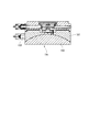
切断装置としてのワイヤソー装置16は、互いに中心軸が平行であって同一水平面内に配設された第1および第2メインローラ11,12と、第1および第2メインローラ11,12の下方であって、第1および第2メインローラ11,12の中間位置に設けられた単一のサブローラ17と、第1および第2メインローラ11,12と単一のサブローラ17に巻回して張設されたワイヤ18と、保持具14を昇降させる昇降装置19とを備える(図1および図2)。
切断装置としてのワイヤソー装置16は、互いに中心軸が平行であって同一水平面内に配設された第1および第2メインローラ11,12と、第1および第2メインローラ11,12の下方であって、第1および第2メインローラ11,12の中間位置に設けられた単一のサブローラ17と、第1および第2メインローラ11,12と単一のサブローラ17に巻回して張設されたワイヤ18と、保持具14を昇降させる昇降装置19とを備える(図1および図2)。
また、第1および第2メインローラ11,12と単一のサブローラ17の外周面には、各ローラ11,12,17の軸方向に所定の間隔をあけて、即ちスライスされるウェーハの厚さ分だけ各ローラ11,12,17の軸方向に間隔をあけて、円周方向に延びる複数本のリング溝(図示せず)が形成される。
ワイヤ18は、繰出しボビン21(図2)に巻付けられた1本の長尺ものであり、この繰出しボビン21から繰出されたワイヤ18は、第1および第2メインローラ11,12と単一のサブローラ17の一端側の各リング溝から他端側の各リング溝に向って順に収容されるように、これらのローラ11,12,17に略逆三角形状であって螺旋状に巻回して張設された後に、巻取りボビン22(図2)に巻取られるように構成される。
ワイヤ18は、繰出しボビン21(図2)に巻付けられた1本の長尺ものであり、この繰出しボビン21から繰出されたワイヤ18は、第1および第2メインローラ11,12と単一のサブローラ17の一端側の各リング溝から他端側の各リング溝に向って順に収容されるように、これらのローラ11,12,17に略逆三角形状であって螺旋状に巻回して張設された後に、巻取りボビン22(図2)に巻取られるように構成される。
保持具14は、インゴット13に接着されるスライス台14aと、このスライス台14aを保持するワークプレート14bとを有する。スライス台14aはインゴット13と同じ材質か、或いはガラス、セラミック、カーボンまたはレジン等により形成されるが、コスト面や成形の容易さを考慮し、カーボンやレジン等が多く用いられる。また接着剤としては、エポキシ樹脂、熱可塑性ワックス等が用いられ、ワークプレート14bは主にSUSにより形成される。さらに、上記昇降装置19は、鉛直方向に延びて設けられた支持部材19aと、この支持部材19aに昇降可能に取付けられ、先端下面に保持具14を保持する水平部材19bとを有する。これにより保持具14に接着されたインゴット13が昇降装置19により昇降可能に構成される。
一般に、インゴット13の結晶方位には多少のばらつきがあり、インゴット13の円柱の中心軸線と必ずしも一致しない。そのため、インゴット13の円柱の中心軸線の向きに合わせてスライス台14aを接着し、ワイヤソー装置16に取り付けてスライスすると、インゴット13から切り出されたウェーハの切断面は結晶格子面と一致せず、これによりウェーハの特性がばらつくという問題がある。
この問題を解消する方法の一つとして、ゴニオ角設定器19cを用いる方法が知られている。
この問題を解消する方法の一つとして、ゴニオ角設定器19cを用いる方法が知られている。
ゴニオ角設定器19cは、水平部材19bの下面に装着されており、ワイヤソー装置16に取り付けられた状態の保持具14の取り付け角度を、ワイヤ18と直交する面内で調整することができる。具体的には、ゴニオ角設定器19cは、図3に示すように、固定部材191、および可動部材192を備える。
固定部材191は、水平部材19bに取り付けられている。
固定部材191の下面は、凹曲面とされ、凹曲面は、ワイヤ18の走行方向に直交する面内で円弧状の断面を有する円筒状の凹曲面とされる。
固定部材191は、水平部材19bに取り付けられている。
固定部材191の下面は、凹曲面とされ、凹曲面は、ワイヤ18の走行方向に直交する面内で円弧状の断面を有する円筒状の凹曲面とされる。
固定部材191の下面には、可動部材192が取り付けられている。可動部材192は、固定部材191の下面に形成された凹曲面に倣う凸曲面を上面に有し、固定部材191に対して、可動部材192を可動させると、ワイヤ18の走行方向に直交する面内で可動部材192を垂直方向に調整することができる。
可動部材192の調整に際しては、垂直方向シャフト193を回転させ、中央に形成された送りねじの螺合位置を変更する。これにより、可動部材192は、ワイヤ18と直交する面内で固定部材191の曲面に沿って移動し、垂直方向の位置調整が可能となる。
ゴニオ角設定器19cによれば、インゴット13の結晶方位に対して、ワイヤ18と直交する面内で適正な向きとなるようにワイヤ18の走行方向を調整することができる。
可動部材192の調整に際しては、垂直方向シャフト193を回転させ、中央に形成された送りねじの螺合位置を変更する。これにより、可動部材192は、ワイヤ18と直交する面内で固定部材191の曲面に沿って移動し、垂直方向の位置調整が可能となる。
ゴニオ角設定器19cによれば、インゴット13の結晶方位に対して、ワイヤ18と直交する面内で適正な向きとなるようにワイヤ18の走行方向を調整することができる。
このように構成されたワイヤソー装置16を用いてシリコン単結晶インゴット13をスライスする方法を説明する。
まず、第1および第2メインローラ11,12と単一のサブローラ17の間にワイヤ18を巻回して張設する。これによりワイヤ18のうち、第1および第2メインローラ11,12の間に水平に張設されたワイヤ18が、第1および第2メインローラ11,12と単一のサブローラ17の回転により水平方向に移動する。
次に、昇降装置19の水平部材19bの先端下面に装備されたゴニオ角設定器19cに、インゴット13とスライス台14aが接着されたワークプレート14bを、ボルト締め等の固定手段により装着する。
まず、第1および第2メインローラ11,12と単一のサブローラ17の間にワイヤ18を巻回して張設する。これによりワイヤ18のうち、第1および第2メインローラ11,12の間に水平に張設されたワイヤ18が、第1および第2メインローラ11,12と単一のサブローラ17の回転により水平方向に移動する。
次に、昇降装置19の水平部材19bの先端下面に装備されたゴニオ角設定器19cに、インゴット13とスライス台14aが接着されたワークプレート14bを、ボルト締め等の固定手段により装着する。
ここで、インゴット13のスライス台14aへの接着方法を詳しく説明する。
まず、インゴット13の円柱の中心軸回りに所定の回転角度だけ回転させ、接着する。所定の回転角度は、ワイヤソー装置16によりスライスして得られたウェーハ23の反り量が所定量になるように決定する。
この決定は、予め実験により上記所定の回転角度の変化に対するウェーハ23の反り量の変化についての相関関係を求め、上記所定の回転角度をこの相関関係から決定することが好ましい。また、インゴット13の結晶軸13bからオリエンテーションフラット13cに下ろした垂線を基準線13dとし、この基準線13dに対する所定の回転角度θ(図5および図6)を45~55度、125~135度、225~235度、および305~315度のいずれかの範囲内に設定することが好ましい。
ただし、通常、インゴット13にスライス台14aを接着するときは、オリエンテーションフラット13cを避けて接着するため、上記基準線13dに対する所定の回転角度θを45~55度、または305~315度の範囲内に設定することが好ましい。
ここで、上記基準線13dに対する所定の回転角度θを上記範囲内に限定したのは、ワイヤ18がインゴット13の劈開面13eの方向に逸れ易くなり、このインゴット13をスライスして得られたウェーハ23の反り量のバラツキが大きくなるからである。
まず、インゴット13の円柱の中心軸回りに所定の回転角度だけ回転させ、接着する。所定の回転角度は、ワイヤソー装置16によりスライスして得られたウェーハ23の反り量が所定量になるように決定する。
この決定は、予め実験により上記所定の回転角度の変化に対するウェーハ23の反り量の変化についての相関関係を求め、上記所定の回転角度をこの相関関係から決定することが好ましい。また、インゴット13の結晶軸13bからオリエンテーションフラット13cに下ろした垂線を基準線13dとし、この基準線13dに対する所定の回転角度θ(図5および図6)を45~55度、125~135度、225~235度、および305~315度のいずれかの範囲内に設定することが好ましい。
ただし、通常、インゴット13にスライス台14aを接着するときは、オリエンテーションフラット13cを避けて接着するため、上記基準線13dに対する所定の回転角度θを45~55度、または305~315度の範囲内に設定することが好ましい。
ここで、上記基準線13dに対する所定の回転角度θを上記範囲内に限定したのは、ワイヤ18がインゴット13の劈開面13eの方向に逸れ易くなり、このインゴット13をスライスして得られたウェーハ23の反り量のバラツキが大きくなるからである。
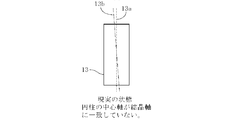
ところが、円柱状のインゴット13において、その円柱の中心軸13aがその結晶軸13bに一致する理想の状態(図4(Z軸)、図9A)になることは殆どなく、その円柱の中心軸13aがその結晶軸13bに一致しない現実の状態(図4(P1―P2)、図9B)になることが殆どである。通常、インゴット13の円柱の中心軸13aとインゴット13の結晶軸13bの傾斜角度は、最大で3度程度である。
一方、スライスされたウェーハ23の表面は、インゴット13の結晶軸13bに垂直な面であることが求められている(図9C)。
一方、スライスされたウェーハ23の表面は、インゴット13の結晶軸13bに垂直な面であることが求められている(図9C)。
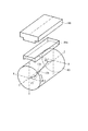
このため、前記インゴット13をインゴット13の円柱の中心軸13aの回りに前記所定の回転角度だけ回転させ、スライス台14aに接着すると、インゴット13の結晶軸13bは、スライス台14aの長手方向からずれた状態となる(図4)。
そのずれに対し、水平方向(図4のXZ面)はスライス台14aとワークプレート14bの接着方向を補正し、インゴット13の結晶軸13bが、図4のYZ面内になるよう接着する。
そのずれに対し、水平方向(図4のXZ面)はスライス台14aとワークプレート14bの接着方向を補正し、インゴット13の結晶軸13bが、図4のYZ面内になるよう接着する。
次にこのインゴット13を、上記第1および第2メインローラ11,12の間に水平に張設されたワイヤ18の上方であって第1および第2メインローラ11,12の各中心軸を通る鉛直線の間にインゴット13の結晶軸13bが第1および第2メインローラ11,12の各中心軸にほぼ平行になるように移動させる(図1および図2)。このときインゴット13の結晶軸13bを含む鉛直面を、第1および第2メインローラ11,12間のワイヤ18の延びる方向に対して直交させる(図9C)。
さらに、保持具14を固定するゴニオ角設定器19cにより、結晶軸13bが第1および第2メインローラ11,12の各中心軸と平行になるよう、保持具14の固定角度を調整する。
換言すれば、第1および第2メインローラ11,12間のワイヤ18と、このワイヤ18によるインゴット13の切断方向とが作る平面に対してインゴット13の結晶軸13bを直交させる。さらにこの状態でインゴット13を鉛直方向に下降させて上記水平方向に移動するワイヤ18を横断する位置まで移動させることにより、インゴット13をスライスする。これにより、インゴット13をスライスした後のウェーハ23の反り量を所望の量に精度良く制御できる。
換言すれば、第1および第2メインローラ11,12間のワイヤ18と、このワイヤ18によるインゴット13の切断方向とが作る平面に対してインゴット13の結晶軸13bを直交させる。さらにこの状態でインゴット13を鉛直方向に下降させて上記水平方向に移動するワイヤ18を横断する位置まで移動させることにより、インゴット13をスライスする。これにより、インゴット13をスライスした後のウェーハ23の反り量を所望の量に精度良く制御できる。
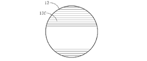
ここで、インゴット13の劈開面13eがウェーハ23表面のワイヤマーク13fと平行であっても、このインゴット13をスライスして得られたウェーハ23の反り量が異なる場合がある。その理由を図5~図8に基づいて説明する。
図7Aおよび図8Aに示すように、インゴット13の劈開面13eがインゴット13の表面のワイヤマーク13fと平行であっても、インゴット13の劈開面13eが、図7Bに示すようにインゴット13の結晶軸13bに対して傾斜する場合と、図8Bに示すようにインゴット13の結晶軸13bに対して平行である場合とがある。
図7Aおよび図8Aに示すように、インゴット13の劈開面13eがインゴット13の表面のワイヤマーク13fと平行であっても、インゴット13の劈開面13eが、図7Bに示すようにインゴット13の結晶軸13bに対して傾斜する場合と、図8Bに示すようにインゴット13の結晶軸13bに対して平行である場合とがある。
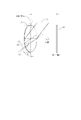
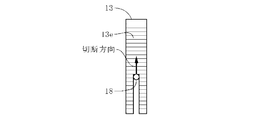
そして、インゴット13の劈開面13eがインゴット13の結晶軸13bに対して傾斜する場合(図7B)、このインゴット13をスライスすると、ワイヤ18が図5の斜視図(a)の破線矢印および図7Cの実線矢印で示す切断方向に対して、図5の斜視図(a)の実線矢印および図7Cの破線矢印で示す方向、即ち劈開面13eの方向に逸れ易い。
これに対して、インゴット13の劈開面13eがインゴット13の結晶軸13bに対して平行である場合(図8B)、このインゴット13をスライスすると、ワイヤ18が図6の斜視図(a)の破線矢印および図8Cの実線矢印で示す切断方向に対して逸れ難く、切断方向に真っ直ぐに進む。
これに対して、インゴット13の劈開面13eがインゴット13の結晶軸13bに対して平行である場合(図8B)、このインゴット13をスライスすると、ワイヤ18が図6の斜視図(a)の破線矢印および図8Cの実線矢印で示す切断方向に対して逸れ難く、切断方向に真っ直ぐに進む。
この結果、インゴット13の劈開面13eがインゴット13表面のワイヤマーク13fと平行であっても(図7A)、インゴット13の劈開面13eが、図7Bに示すようにインゴット13の結晶軸13bに対して傾斜していると、このインゴット13をスライスして得られたウェーハ23は図5の側面図(b)に示すように反ってしまう。
これに対して、インゴット13の劈開面13eがインゴット13表面のワイヤマーク13fと平行であっても(図8A)、インゴット13の劈開面13eが、図8Bに示すようにインゴット13の結晶軸13bに対して平行であると、このインゴット13をスライスして得られたウェーハ23は図6の側面図(b)に示すように反らない。なお、インゴット13の劈開面13eが、図8Bに示すようにインゴット13の結晶軸13bに対して平行でなくても、平行に近い角度であれば、スライスして得られたウェーハ23は反り難い。
これに対して、インゴット13の劈開面13eがインゴット13表面のワイヤマーク13fと平行であっても(図8A)、インゴット13の劈開面13eが、図8Bに示すようにインゴット13の結晶軸13bに対して平行であると、このインゴット13をスライスして得られたウェーハ23は図6の側面図(b)に示すように反らない。なお、インゴット13の劈開面13eが、図8Bに示すようにインゴット13の結晶軸13bに対して平行でなくても、平行に近い角度であれば、スライスして得られたウェーハ23は反り難い。
一方、インゴット13の結晶軸13bを中心とする所定の回転角度を、ワイヤソー装置16によりインゴット13をスライスして得られたウェーハ23の反り量が最小になるように決定してもよい。例えば、インゴット13の結晶軸13bが<111>である場合、この結晶軸13bからオリエンテーションフラット13cに下ろした垂線を基準線13dとし、この基準線13dに対する所定の回転角度θ(図5および図6)を45~55度の範囲内とすると、インゴット13をスライスした後のウェーハ23の反り量を低減できる。
上記実施の形態では、半導体単結晶インゴットとして、シリコン単結晶インゴットを挙げたが、炭化珪素(SiC)単結晶インゴット、ガリウムヒ素(GaAs)単結晶インゴット、サファイア単結晶インゴット等でもよい。
また、上記実施の形態では、インゴットの結晶軸からオリエンテーションフラットに下ろした垂線を基準線として、インゴットの結晶軸を中心とする所定の回転角度を決定したが、インゴットの結晶軸からノッチに下ろした垂線を基準線として、インゴットの結晶軸を中心とする所定の回転角度を決定してもよい。
さらに、オリエンテーションフラットやノッチを代替する回転基準部があれば、インゴットの結晶軸からこの回転基準部に下ろした垂線を基準線として、インゴットの結晶軸を中心とする所定の回転角を決定してもよい。
また、上記実施の形態では、インゴットの結晶軸からオリエンテーションフラットに下ろした垂線を基準線として、インゴットの結晶軸を中心とする所定の回転角度を決定したが、インゴットの結晶軸からノッチに下ろした垂線を基準線として、インゴットの結晶軸を中心とする所定の回転角度を決定してもよい。
さらに、オリエンテーションフラットやノッチを代替する回転基準部があれば、インゴットの結晶軸からこの回転基準部に下ろした垂線を基準線として、インゴットの結晶軸を中心とする所定の回転角を決定してもよい。
次に本発明の実施例を比較例とともに詳しく説明する。
<実施例1>
図1および図2に示すように、直径が150mmであり結晶軸が<111>である円柱状のシリコン単結晶インゴット13を用意した。このインゴット13の円柱の中心軸13aを中心として所定の回転角度だけ回転させた状態でインゴット13とスライス台14aを接着した。さらにスライス台14aとワークプレート14bを、水平方向(図4のXZ面)の接着方向を補正して、インゴット13の結晶軸が、図4のYZ面内になるよう接着した。さらに、インゴット13を接着した保持具14をゴニオ角設定器19cに取付け固定し、ゴニオ角設定器19cにより、結晶軸13bが第1および第2メインローラ11,12の各中心軸と平行になるよう、保持具14の固定角度を調整した。
<実施例1>
図1および図2に示すように、直径が150mmであり結晶軸が<111>である円柱状のシリコン単結晶インゴット13を用意した。このインゴット13の円柱の中心軸13aを中心として所定の回転角度だけ回転させた状態でインゴット13とスライス台14aを接着した。さらにスライス台14aとワークプレート14bを、水平方向(図4のXZ面)の接着方向を補正して、インゴット13の結晶軸が、図4のYZ面内になるよう接着した。さらに、インゴット13を接着した保持具14をゴニオ角設定器19cに取付け固定し、ゴニオ角設定器19cにより、結晶軸13bが第1および第2メインローラ11,12の各中心軸と平行になるよう、保持具14の固定角度を調整した。
インゴット13の結晶軸13bは、照射して結晶面で反射してくるX線の角度により検出した。またインゴット13を保持具14に接着するときの所定の回転角度を決定した。
さらに、上記所定の回転角度は、インゴット13の結晶軸13bからオリエンテーションフラット13cに下ろした垂線を基準線13dとするとき、この基準線13dに対する回転角度θ(図5および図6)とした。
具体的には、インゴット13を、ワイヤソー装置16の第1および第2メインローラ11,12の間に水平に張設されたワイヤ18の上方であって第1および第2メインローラ11,12の各中心軸を通る鉛直線の間にインゴット13の結晶軸13bが第1および第2メインローラ11,12の各中心軸にほぼ平行になるように移動させた(図1および図2)。このときインゴット13の結晶軸13bを含む鉛直面を、第1および第2メインローラ11,12間のワイヤ18の延びる方向に対して直交させた(図9C)。
さらに、上記所定の回転角度は、インゴット13の結晶軸13bからオリエンテーションフラット13cに下ろした垂線を基準線13dとするとき、この基準線13dに対する回転角度θ(図5および図6)とした。
具体的には、インゴット13を、ワイヤソー装置16の第1および第2メインローラ11,12の間に水平に張設されたワイヤ18の上方であって第1および第2メインローラ11,12の各中心軸を通る鉛直線の間にインゴット13の結晶軸13bが第1および第2メインローラ11,12の各中心軸にほぼ平行になるように移動させた(図1および図2)。このときインゴット13の結晶軸13bを含む鉛直面を、第1および第2メインローラ11,12間のワイヤ18の延びる方向に対して直交させた(図9C)。
そして、インゴット13を接着した保持具14を、ゴニオ角設定器19cに取り付け固定し、ゴニオ角設定器19cにより、結晶軸13bが第1および第2ローラ11,12の各中心軸線と平行になるよう、保持具14の固定角を調整した。
このインゴット13を鉛直方向に下降させて上記水平方向に移動するワイヤ18を横断する位置まで移動させることにより、インゴット13をスライスしてウェーハ23を作製した。上記所定の回転角度θを45~55度に調整して、上記と同様にインゴット13をスライスしてウェーハ23を作製した。これらのウェーハ23を実施例1とした。
このインゴット13を鉛直方向に下降させて上記水平方向に移動するワイヤ18を横断する位置まで移動させることにより、インゴット13をスライスしてウェーハ23を作製した。上記所定の回転角度θを45~55度に調整して、上記と同様にインゴット13をスライスしてウェーハ23を作製した。これらのウェーハ23を実施例1とした。
<比較例1>
インゴットの円柱の中心軸とは異なるインゴットの結晶軸を中心として任意の回転角度だけ回転させた状態で保持具により接着保持したことと、インゴット13を接着した保持具14をゴニオ角設定器19cに取り付け固定した後、ゴニオ角設定器19cによる保持具14の固定角度を調整しなかったこと以外は、実施例1と同様にしてインゴットをスライスしてウェーハを作製した。これらのウェーハを比較例1とした。
インゴットの円柱の中心軸とは異なるインゴットの結晶軸を中心として任意の回転角度だけ回転させた状態で保持具により接着保持したことと、インゴット13を接着した保持具14をゴニオ角設定器19cに取り付け固定した後、ゴニオ角設定器19cによる保持具14の固定角度を調整しなかったこと以外は、実施例1と同様にしてインゴットをスライスしてウェーハを作製した。これらのウェーハを比較例1とした。
<試験1および評価>
実施例1および比較例1のウェーハの反り量を測定した。このウェーハの反り量は、ウェーハの裏面において、ウェーハの外周縁から内側に3mm内側の位置であって、ウェーハの結晶軸を中心に120度間隔に採った3点を通る平面を想定し、この平面から測定したウェーハの反りの大きさのうち最大値とした。その結果を図10に示す。
実施例1および比較例1のウェーハの反り量を測定した。このウェーハの反り量は、ウェーハの裏面において、ウェーハの外周縁から内側に3mm内側の位置であって、ウェーハの結晶軸を中心に120度間隔に採った3点を通る平面を想定し、この平面から測定したウェーハの反りの大きさのうち最大値とした。その結果を図10に示す。
図10から明らかなように、比較例1では、所定の回転角度の範囲内でウェーハの反り量が小さかったけれども、所定の回転角度の範囲外でウェーハの反り量が大きかったのに対し、実施例1では、回転角度θを45~55度に調整することにより、ウェーハの反り量が全て小さくなった。
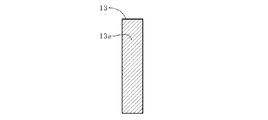
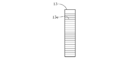
13…シリコン単結晶インゴット(半導体単結晶インゴット)
13a…中心軸
13b…結晶軸
13c…オリエンテーションフラット(回転基準部)
13d…基準線
14…保持具
16…ワイヤソー装置(切断装置)
19c…ゴニオ角設定器
13a…中心軸
13b…結晶軸
13c…オリエンテーションフラット(回転基準部)
13d…基準線
14…保持具
16…ワイヤソー装置(切断装置)
19c…ゴニオ角設定器
Claims (4)
- 円柱状の半導体単結晶インゴットを、このインゴットの円柱の中心軸とは異なる前記インゴットの結晶軸を中心として所定の回転角度だけ回転させた状態で保持具により接着保持し、この状態で前記インゴットを切断装置によりスライスする半導体単結晶インゴットのスライス方法において、
前記切断装置によりスライスされたウェーハの反り量が所定量になるように、前記インゴットを前記保持具により接着保持するときの前記所定の回転角度と、前記切断装置による前記保持具の傾け角度を決定することを特徴とする半導体単結晶インゴットのスライス方法。 - 請求項1に記載の半導体単結晶インゴットのスライス方法において、
予め実験により前記所定の回転角度の変化に対する前記ウェーハの反り量の変化についての相関関係を求め、前記所定の回転角度を前記相関関係から決定する半導体単結晶インゴットのスライス方法。 - 請求項1に記載の半導体単結晶インゴットのスライス方法において、
前記切断装置によりスライスされたウェーハの反り量が最小になるように、前記インゴットを前記保持具により接着保持するときの前記所定の回転角度を決定する半導体単結晶インゴットのスライス方法。 - 請求項1に記載の半導体単結晶インゴットのスライス方法において、
前記インゴットに回転基準部を形成し、前記インゴットの結晶軸から前記回転基準部に下ろした垂線を基準線とするとき、この基準線に対する前記所定の回転角度が45~55度、125~135度、225~235度、および305~315度のいずれかの範囲である半導体単結晶インゴットのスライス方法。
Priority Applications (4)
| Application Number | Priority Date | Filing Date | Title |
|---|---|---|---|
| CN201880088365.0A CN111801771B (zh) | 2018-02-27 | 2018-02-27 | 半导体单晶锭的切片方法 |
| PCT/JP2018/007074 WO2019167100A1 (ja) | 2018-02-27 | 2018-02-27 | 半導体単結晶インゴットのスライス方法 |
| JP2020503110A JP6923067B2 (ja) | 2018-02-27 | 2018-02-27 | 半導体単結晶インゴットのスライス方法 |
| TW108102372A TWI750447B (zh) | 2018-02-27 | 2019-01-22 | 半導體單結晶鑄錠的切片方法 |
Applications Claiming Priority (1)
| Application Number | Priority Date | Filing Date | Title |
|---|---|---|---|
| PCT/JP2018/007074 WO2019167100A1 (ja) | 2018-02-27 | 2018-02-27 | 半導体単結晶インゴットのスライス方法 |
Publications (1)
| Publication Number | Publication Date |
|---|---|
| WO2019167100A1 true WO2019167100A1 (ja) | 2019-09-06 |
Family
ID=67805280
Family Applications (1)
| Application Number | Title | Priority Date | Filing Date |
|---|---|---|---|
| PCT/JP2018/007074 Ceased WO2019167100A1 (ja) | 2018-02-27 | 2018-02-27 | 半導体単結晶インゴットのスライス方法 |
Country Status (4)
| Country | Link |
|---|---|
| JP (1) | JP6923067B2 (ja) |
| CN (1) | CN111801771B (ja) |
| TW (1) | TWI750447B (ja) |
| WO (1) | WO2019167100A1 (ja) |
Cited By (4)
| Publication number | Priority date | Publication date | Assignee | Title |
|---|---|---|---|---|
| CN113771247A (zh) * | 2021-09-07 | 2021-12-10 | 麦斯克电子材料股份有限公司 | 一种12寸半导体晶圆的切割方法 |
| CN113787636A (zh) * | 2021-07-09 | 2021-12-14 | 麦斯克电子材料股份有限公司 | 一种用于12寸半导体晶圆的手动粘棒方法 |
| CN119550490A (zh) * | 2024-10-25 | 2025-03-04 | 上海新昇半导体科技有限公司 | <111>型晶棒粘贴方法及粘棒机系统 |
| TWI877716B (zh) * | 2022-08-26 | 2025-03-21 | 日商Sumco股份有限公司 | 圓柱磨削裝置、圓柱磨削方法及晶圓的製造方法 |
Families Citing this family (1)
| Publication number | Priority date | Publication date | Assignee | Title |
|---|---|---|---|---|
| KR102283879B1 (ko) * | 2021-01-14 | 2021-07-29 | 에스케이씨 주식회사 | 탄화규소 웨이퍼의 제조방법, 탄화규소 웨이퍼 및 웨이퍼 제조용 시스템 |
Citations (3)
| Publication number | Priority date | Publication date | Assignee | Title |
|---|---|---|---|---|
| JP2001050912A (ja) * | 1999-08-11 | 2001-02-23 | Rigaku Corp | 単結晶インゴットの支持装置、単結晶インゴットの測定装置及び単結晶インゴットの測定方法 |
| JP2014195025A (ja) * | 2013-03-29 | 2014-10-09 | Sumco Techxiv株式会社 | 半導体単結晶インゴットのスライス方法 |
| JP2017024145A (ja) * | 2015-07-27 | 2017-02-02 | 信越半導体株式会社 | ワークホルダー及びワークの切断方法 |
Family Cites Families (6)
| Publication number | Priority date | Publication date | Assignee | Title |
|---|---|---|---|---|
| CH692331A5 (de) * | 1996-06-04 | 2002-05-15 | Tokyo Seimitsu Co Ltd | Drahtsäge und Schneidverfahren unter Einsatz derselben. |
| DE10128630A1 (de) * | 2001-06-13 | 2003-01-02 | Freiberger Compound Mat Gmbh | Vorrichtung und Verfahren zur Bestimmung der Orientierung einer kristallografischen Ebene relativ zu einer Kristalloberfläche sowie Vorrichtung und Verfahren zum Trennen eines Einkristalls in einer Trennmaschine |
| JP6115748B2 (ja) * | 2012-07-04 | 2017-04-19 | 東芝Itコントロールシステム株式会社 | 結晶方位測定装置 |
| JP6099960B2 (ja) * | 2012-12-18 | 2017-03-22 | ダイトエレクトロン株式会社 | ウェーハの面取り加工方法およびウェーハの面取り装置 |
| JP6318637B2 (ja) * | 2014-01-17 | 2018-05-09 | 日立金属株式会社 | 高硬度材料のマルチワイヤソーによる切断方法 |
| JP6424703B2 (ja) * | 2015-03-27 | 2018-11-21 | 株式会社Sumco | シリコンウェーハの製造方法 |
-
2018
- 2018-02-27 WO PCT/JP2018/007074 patent/WO2019167100A1/ja not_active Ceased
- 2018-02-27 JP JP2020503110A patent/JP6923067B2/ja active Active
- 2018-02-27 CN CN201880088365.0A patent/CN111801771B/zh active Active
-
2019
- 2019-01-22 TW TW108102372A patent/TWI750447B/zh active
Patent Citations (3)
| Publication number | Priority date | Publication date | Assignee | Title |
|---|---|---|---|---|
| JP2001050912A (ja) * | 1999-08-11 | 2001-02-23 | Rigaku Corp | 単結晶インゴットの支持装置、単結晶インゴットの測定装置及び単結晶インゴットの測定方法 |
| JP2014195025A (ja) * | 2013-03-29 | 2014-10-09 | Sumco Techxiv株式会社 | 半導体単結晶インゴットのスライス方法 |
| JP2017024145A (ja) * | 2015-07-27 | 2017-02-02 | 信越半導体株式会社 | ワークホルダー及びワークの切断方法 |
Cited By (5)
| Publication number | Priority date | Publication date | Assignee | Title |
|---|---|---|---|---|
| CN113787636A (zh) * | 2021-07-09 | 2021-12-14 | 麦斯克电子材料股份有限公司 | 一种用于12寸半导体晶圆的手动粘棒方法 |
| CN113787636B (zh) * | 2021-07-09 | 2022-05-27 | 麦斯克电子材料股份有限公司 | 一种用于12寸半导体晶圆的手动粘棒方法 |
| CN113771247A (zh) * | 2021-09-07 | 2021-12-10 | 麦斯克电子材料股份有限公司 | 一种12寸半导体晶圆的切割方法 |
| TWI877716B (zh) * | 2022-08-26 | 2025-03-21 | 日商Sumco股份有限公司 | 圓柱磨削裝置、圓柱磨削方法及晶圓的製造方法 |
| CN119550490A (zh) * | 2024-10-25 | 2025-03-04 | 上海新昇半导体科技有限公司 | <111>型晶棒粘贴方法及粘棒机系统 |
Also Published As
| Publication number | Publication date |
|---|---|
| TWI750447B (zh) | 2021-12-21 |
| JPWO2019167100A1 (ja) | 2021-02-04 |
| CN111801771A (zh) | 2020-10-20 |
| JP6923067B2 (ja) | 2021-08-18 |
| CN111801771B (zh) | 2024-04-26 |
| TW201936350A (zh) | 2019-09-16 |
Similar Documents
| Publication | Publication Date | Title |
|---|---|---|
| JP6132621B2 (ja) | 半導体単結晶インゴットのスライス方法 | |
| WO2019167100A1 (ja) | 半導体単結晶インゴットのスライス方法 | |
| CN107848092B (zh) | 工件支架及工件的切断方法 | |
| JP6572827B2 (ja) | 単結晶インゴットの切断方法 | |
| JP7822137B2 (ja) | 亀裂低減に最適な格子面配向を持つSiC結晶基板およびその製造方法 | |
| CN105814669A (zh) | 工件的切断方法及工件保持夹具 | |
| JP2013258243A (ja) | 化合物半導体基板の製造方法および製造装置 | |
| JP6230112B2 (ja) | ウェハの製造方法およびウェハの製造装置 | |
| CN115946251B (zh) | 用于线切割硅棒的方法、设备及硅片 | |
| US8844511B2 (en) | Method for slicing a multiplicity of wafers from a crystal composed of semiconductor material | |
| JP6614298B2 (ja) | シリコンウェーハの製造方法 | |
| JP2009186181A (ja) | 結晶方位測定装置、結晶加工装置及び結晶加工方法 | |
| JP7655808B2 (ja) | 亀裂低減に最適な格子面配向を持つSiC結晶およびその製造方法 | |
| CN109531844B (zh) | 多线切割装置、多线切割方法及其用途 | |
| KR100526215B1 (ko) | 실리콘 단결정 웨이퍼의 제조방법 및 제조장치 | |
| JP2016186956A (ja) | シリコンウェーハの製造方法 | |
| JP2011216819A (ja) | 炭化珪素単結晶基板の製造方法 | |
| JP5381183B2 (ja) | 半導体インゴットのスライス方法 | |
| JP4797276B2 (ja) | 単結晶インゴットの切断方法 | |
| CN114833607A (zh) | 夹具及切割机 | |
| JP2009194137A (ja) | 半導体ウェハの製造方法 | |
| JP2005231248A (ja) | 単結晶切断方法 | |
| WO2015040695A1 (ja) | 化合物半導体基板の製造方法および製造装置 | |
| JPH02182406A (ja) | 半導体切断面形状制御装置 | |
| JP2001351836A (ja) | 半導体ウエハーおよびその製造方法 |
Legal Events
| Date | Code | Title | Description |
|---|---|---|---|
| 121 | Ep: the epo has been informed by wipo that ep was designated in this application |
Ref document number: 18907937 Country of ref document: EP Kind code of ref document: A1 |
|
| ENP | Entry into the national phase |
Ref document number: 2020503110 Country of ref document: JP Kind code of ref document: A |
|
| NENP | Non-entry into the national phase |
Ref country code: DE |
|
| 122 | Ep: pct application non-entry in european phase |
Ref document number: 18907937 Country of ref document: EP Kind code of ref document: A1 |