WO2019159693A1 - 撮像モジュール、内視鏡、及びカテーテル - Google Patents
撮像モジュール、内視鏡、及びカテーテル Download PDFInfo
- Publication number
- WO2019159693A1 WO2019159693A1 PCT/JP2019/003131 JP2019003131W WO2019159693A1 WO 2019159693 A1 WO2019159693 A1 WO 2019159693A1 JP 2019003131 W JP2019003131 W JP 2019003131W WO 2019159693 A1 WO2019159693 A1 WO 2019159693A1
- Authority
- WO
- WIPO (PCT)
- Prior art keywords
- light emitting
- imaging module
- light
- emitting element
- solid
- Prior art date
- Legal status (The legal status is an assumption and is not a legal conclusion. Google has not performed a legal analysis and makes no representation as to the accuracy of the status listed.)
- Ceased
Links
Images



Classifications
-
- A—HUMAN NECESSITIES
- A61—MEDICAL OR VETERINARY SCIENCE; HYGIENE
- A61B—DIAGNOSIS; SURGERY; IDENTIFICATION
- A61B1/00—Instruments for performing medical examinations of the interior of cavities or tubes of the body by visual or photographical inspection, e.g. endoscopes; Illuminating arrangements therefor
- A61B1/00064—Constructional details of the endoscope body
- A61B1/00071—Insertion part of the endoscope body
- A61B1/0008—Insertion part of the endoscope body characterised by distal tip features
- A61B1/00096—Optical elements
-
- A—HUMAN NECESSITIES
- A61—MEDICAL OR VETERINARY SCIENCE; HYGIENE
- A61B—DIAGNOSIS; SURGERY; IDENTIFICATION
- A61B1/00—Instruments for performing medical examinations of the interior of cavities or tubes of the body by visual or photographical inspection, e.g. endoscopes; Illuminating arrangements therefor
- A61B1/06—Instruments for performing medical examinations of the interior of cavities or tubes of the body by visual or photographical inspection, e.g. endoscopes; Illuminating arrangements therefor with illuminating arrangements
-
- A—HUMAN NECESSITIES
- A61—MEDICAL OR VETERINARY SCIENCE; HYGIENE
- A61B—DIAGNOSIS; SURGERY; IDENTIFICATION
- A61B1/00—Instruments for performing medical examinations of the interior of cavities or tubes of the body by visual or photographical inspection, e.g. endoscopes; Illuminating arrangements therefor
- A61B1/00112—Connection or coupling means
- A61B1/00114—Electrical cables in or with an endoscope
-
- A—HUMAN NECESSITIES
- A61—MEDICAL OR VETERINARY SCIENCE; HYGIENE
- A61B—DIAGNOSIS; SURGERY; IDENTIFICATION
- A61B1/00—Instruments for performing medical examinations of the interior of cavities or tubes of the body by visual or photographical inspection, e.g. endoscopes; Illuminating arrangements therefor
- A61B1/00112—Connection or coupling means
- A61B1/00121—Connectors, fasteners and adapters, e.g. on the endoscope handle
- A61B1/00124—Connectors, fasteners and adapters, e.g. on the endoscope handle electrical, e.g. electrical plug-and-socket connection
-
- A—HUMAN NECESSITIES
- A61—MEDICAL OR VETERINARY SCIENCE; HYGIENE
- A61B—DIAGNOSIS; SURGERY; IDENTIFICATION
- A61B1/00—Instruments for performing medical examinations of the interior of cavities or tubes of the body by visual or photographical inspection, e.g. endoscopes; Illuminating arrangements therefor
- A61B1/04—Instruments for performing medical examinations of the interior of cavities or tubes of the body by visual or photographical inspection, e.g. endoscopes; Illuminating arrangements therefor combined with photographic or television appliances
-
- A—HUMAN NECESSITIES
- A61—MEDICAL OR VETERINARY SCIENCE; HYGIENE
- A61B—DIAGNOSIS; SURGERY; IDENTIFICATION
- A61B1/00—Instruments for performing medical examinations of the interior of cavities or tubes of the body by visual or photographical inspection, e.g. endoscopes; Illuminating arrangements therefor
- A61B1/04—Instruments for performing medical examinations of the interior of cavities or tubes of the body by visual or photographical inspection, e.g. endoscopes; Illuminating arrangements therefor combined with photographic or television appliances
- A61B1/05—Instruments for performing medical examinations of the interior of cavities or tubes of the body by visual or photographical inspection, e.g. endoscopes; Illuminating arrangements therefor combined with photographic or television appliances characterised by the image sensor, e.g. camera, being in the distal end portion
-
- A—HUMAN NECESSITIES
- A61—MEDICAL OR VETERINARY SCIENCE; HYGIENE
- A61B—DIAGNOSIS; SURGERY; IDENTIFICATION
- A61B1/00—Instruments for performing medical examinations of the interior of cavities or tubes of the body by visual or photographical inspection, e.g. endoscopes; Illuminating arrangements therefor
- A61B1/04—Instruments for performing medical examinations of the interior of cavities or tubes of the body by visual or photographical inspection, e.g. endoscopes; Illuminating arrangements therefor combined with photographic or television appliances
- A61B1/05—Instruments for performing medical examinations of the interior of cavities or tubes of the body by visual or photographical inspection, e.g. endoscopes; Illuminating arrangements therefor combined with photographic or television appliances characterised by the image sensor, e.g. camera, being in the distal end portion
- A61B1/051—Details of CCD assembly
-
- A—HUMAN NECESSITIES
- A61—MEDICAL OR VETERINARY SCIENCE; HYGIENE
- A61B—DIAGNOSIS; SURGERY; IDENTIFICATION
- A61B1/00—Instruments for performing medical examinations of the interior of cavities or tubes of the body by visual or photographical inspection, e.g. endoscopes; Illuminating arrangements therefor
- A61B1/06—Instruments for performing medical examinations of the interior of cavities or tubes of the body by visual or photographical inspection, e.g. endoscopes; Illuminating arrangements therefor with illuminating arrangements
- A61B1/0661—Endoscope light sources
-
- A—HUMAN NECESSITIES
- A61—MEDICAL OR VETERINARY SCIENCE; HYGIENE
- A61B—DIAGNOSIS; SURGERY; IDENTIFICATION
- A61B1/00—Instruments for performing medical examinations of the interior of cavities or tubes of the body by visual or photographical inspection, e.g. endoscopes; Illuminating arrangements therefor
- A61B1/06—Instruments for performing medical examinations of the interior of cavities or tubes of the body by visual or photographical inspection, e.g. endoscopes; Illuminating arrangements therefor with illuminating arrangements
- A61B1/07—Instruments for performing medical examinations of the interior of cavities or tubes of the body by visual or photographical inspection, e.g. endoscopes; Illuminating arrangements therefor with illuminating arrangements using light-conductive means, e.g. optical fibres
-
- G—PHYSICS
- G02—OPTICS
- G02B—OPTICAL ELEMENTS, SYSTEMS OR APPARATUS
- G02B23/00—Telescopes, e.g. binoculars; Periscopes; Instruments for viewing the inside of hollow bodies; Viewfinders; Optical aiming or sighting devices
- G02B23/24—Instruments or systems for viewing the inside of hollow bodies, e.g. fibrescopes
-
- H—ELECTRICITY
- H04—ELECTRIC COMMUNICATION TECHNIQUE
- H04N—PICTORIAL COMMUNICATION, e.g. TELEVISION
- H04N23/00—Cameras or camera modules comprising electronic image sensors; Control thereof
Definitions
- the present invention relates to an imaging module, an endoscope, and a catheter.
- This application claims priority based on Japanese Patent Application No. 2018-024185 for which it applied to Japan on February 14, 2018, and uses the content here.
- an endoscope provided with a light guide fiber bundle for illumination is known (for example, see Patent Document 1).
- a fiber bundle is arranged so as not to interfere with an imaging module composed of a solid-state imaging device, an imaging device holding cylinder, etc., and a space between optical fibers constituting the fiber bundle is filled with a low-viscosity adhesive.
- a light source that supplies light to the fiber bundle is provided behind the endoscope, and light emitted from the light source is guided to the distal end of the endoscope through the fiber bundle.
- the endoscope having the light guide fiber bundle has the following problems. Since the fiber bundle has rigidity, it cannot be bent sufficiently. For this reason, the flexibility of an endoscope falls by using a fiber bundle for an endoscope. When the optical fiber is bent due to the bending of the fiber bundle, the light from the light source cannot be guided to the tip of the fiber bundle. In order to obtain sufficient illuminance, it is necessary to increase the number of optical fibers constituting the fiber bundle. In this case, the cross-sectional area of the fiber bundle increases, and a small-diameter endoscope cannot be provided. Since the fiber bundle is arranged over the entire length of the endoscope, a working channel having a sufficient size cannot be secured in the projection plane of the endoscope. Furthermore, the material cost and assembly cost of the fiber bundle are large, and an inexpensive endoscope cannot be provided.
- One aspect of the present invention has been proposed in view of such a conventional situation, and is a thin imaging module capable of realizing an endoscope with sufficient flexibility and illuminance, and the imaging module.
- An object of the present invention is to provide an endoscope including the above and a catheter including the imaging module.
- an imaging module includes a planar light emitting device having a light emitting surface and a light emitting device terminal, and the planar light emitting device connected to the light emitting device terminal of the planar light emitting device.
- a power supply cable that supplies power to the element, a solid-state image sensor that images an illumination target irradiated by light emitted from the light exit surface of the planar light-emitting element, and the solid-state image sensor
- the planar light emitting device, the solid-state imaging device, a part of the light shielding member, and the light guide portion constitute a rigid portion.
- connection body includes a side terminal in which the embedded conductor is exposed inside a groove formed on a side surface of the main body, and the coaxial cable is electrically connected to the side terminal.
- the planar light emitting elements may be arranged adjacent to the coaxial cable in a rear region facing the coaxial cable behind the connection body.
- the imaging module includes a lens unit that forms an image of reflected light from the illumination target on a light receiving surface of the solid-state imaging element, and the planar light-emitting element is the lens unit or the solid-state imaging. It may be arranged next to the element.
- the power supply cable includes a conductive wire connected to the light emitting element terminal, a conductive wire tip of the conductive line is abutted against the light emitting element terminal, Solder may be formed so as to cover a contact portion between the light emitting element terminal and the conductive wire tip.
- the light emitting element terminal has a terminal outer peripheral portion located at an end portion of the light emitting element terminal, and the conductive wire is located at a position away from the tip of the conductive wire.
- the solder may have a side surface, and the solder may cover the light emitting element terminal and the conductive line so as to form a curved surface extending from the terminal outer periphery toward the side surface.
- the power supply cable may include a shield member that covers the outside of the conductive wire.
- the power supply cable may be a micro coaxial cable.
- the light emitting element terminal and the power supply cable may be covered with a cable reinforcing portion.
- the light shielding member may be made of a light shielding material.
- a light guide plate may be provided on an end surface of the light guide unit.
- the end face of the light guide section may coincide with the end face of the imaging module.
- the imaging module according to the first aspect of the present invention may include a plurality of the planar light emitting elements, and the plurality of planar light emitting elements may be arranged so as to sandwich the solid-state imaging element in plan view.
- the imaging module according to the first aspect of the present invention may include a plurality of the planar light emitting elements, and the plurality of planar light emitting elements may be arranged so as to surround the solid-state imaging element in plan view.
- the imaging module according to the first aspect of the present invention may include a housing that covers the outside of the light shielding member.
- an endoscope according to a second aspect of the present invention includes an imaging module according to the first aspect.
- a catheter according to a third aspect of the present invention includes the imaging module according to the first aspect, an insulating tube surrounding the imaging module, and a channel provided in the tube. .
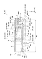
- FIG. 1 and FIG. 2 are views showing a main part of the endoscope 100 according to the first embodiment of the present invention, and are sectional views showing the structure of the imaging module 10.
- FIG. 1 is a sectional view seen from the Y direction
- FIG. 2 is a sectional view seen from the X direction.
- the direction (left side in FIG. 1) from the connection body 30 toward the solid-state imaging device 20 in the Z direction may be referred to as “front” or “front side”.
- the direction from the connecting body 30 toward the coaxial cable 40 (right side in FIG. 1) may be referred to as “rear side” or “rear side”.
- the imaging module 10 includes a solid-state imaging device 20 (imaging device), a connection body 30, two coaxial cables 40 (first coaxial cable 40F and second coaxial cable 40S), a capacitor 50 (electronic component), and a lens unit. 60, an insulating tube 70, a light emitting diode 80, and a light shielding member 90.
- the solid-state image sensor 20 is provided in front of the connection body 30.
- the solid-state imaging device 20 includes a light receiving surface 21 positioned on the upper surface of the solid-state imaging device 20 and four imaging terminals 22 (22A, 22B, 22C, 22D) provided on the lower surface of the solid-state imaging device 20.
- a lens unit 60 is mounted on the light receiving surface 21.
- the imaging terminal 22 is a terminal connected to a mounting pad (described later) provided on the upper surface 31 t of the connection body 30.
- a CMOS complementary metal oxide semiconductor
- the solid-state imaging device 20 is electrically connected to the two coaxial cables 40 via the connection body 30.
- connection body 30 is located between the solid-state imaging device 20 and the coaxial cable 40.
- the connection body 30 includes a main body 31 made of an insulating member, and embedded conductors 33A and 33C (first embedded conductor) and embedded conductors 33B and 33D (second embedded conductor) provided inside the main body 31.
- a groove portion from which the connection body 30 is partially removed is formed on the side surface of the main body 31 .
- side terminals 32A and 32C first side terminals from which the buried conductors 33A and 33C are exposed
- side terminals 32B and 32D second side terminals from which the buried conductors 33B and 33D are exposed, respectively.
- the lower surface 31b of the main body 31 is provided with lower surface terminals 34B and 34D from which the embedded conductors 33B and 33D are exposed.
- the embedded conductors 33A, 33B, 33C, and 33D are electrically connected to the imaging terminals 22A, 22B, 22C, and 22D through mounting pads provided on the upper surface 31t of the connection body 30, respectively.
- the length (X direction and Y direction) of one side of the upper surface 31t of the connection body 30 is 2 mm or less.
- the imaging module 10 includes two coaxial cables 40 (40F, 40S).
- Each of the coaxial cables 40 includes an inner conductor portion 41 (41A, 41C), a covering portion 42 (insulator), and a sheath conductor portion 43 (43B, 43D).
- the coaxial cable 40F includes an inner conductor portion 41A and a sheath conductor portion 43B.
- the coaxial cable 40S includes an inner conductor portion 41C and a sheath conductor portion 43D.
- the length of the inner conductor portion 41, the length of the sheath conductor portion 43, and the length of the covering portion 42 located between the inner conductor portion 41 and the sheath conductor portion 43 are 0.1 to 1.0 mm.
- the inner conductor portion 41, the covering portion 42, and the sheath conductor portion 43 of the coaxial cable 40 are disposed in the groove portion of the connection body 30.
- the inner conductor portion 41A is electrically connected to the side terminal 32A by soldering.
- the sheath conductor portion 43B is electrically connected to the side terminal 32B by soldering.
- the inner conductor portion 41C is electrically connected to the side terminal 32C by soldering.
- the sheath conductor portion 43D is electrically connected to the side terminal 32D by soldering.
- the imaging terminal 22A of the solid-state imaging device 20 is electrically connected to the internal conductor portion 41A via the embedded conductor 33A.
- the imaging terminal 22B of the solid-state imaging device 20 is electrically connected to the sheath conductor portion 43B via the embedded conductor 33B.
- the imaging terminal 22C of the solid-state imaging device 20 is electrically connected to the internal conductor portion 41C via the embedded conductor 33C.
- the imaging terminal 22D of the solid-state imaging device 20 is electrically connected to the sheath conductor portion 43D through the embedded conductor 33D.
- Capacitor 50 The capacitor 50 is provided on the lower surface 31b of the connection body 30 via a mounting pad. The external terminal of the capacitor 50 is connected to the lower surface terminals 34B and 34D. In addition, the resin layer is provided on the lower surface 31b of the connection body 30, and the short circuit between the lower surface terminals 34B and 34D is prevented.
- the lens unit 60 has a configuration in which an objective lens (not shown) is incorporated in a cylindrical barrel (not shown).
- the optical axis of the lens unit 60 is aligned with the light receiving surface 21 of the solid-state imaging device 20.
- One end of the lens barrel in the axial direction is fixed to the cover member 62.
- the lens unit 60 forms an image on the light receiving surface 21 of the solid-state imaging device 20 with light incident from the imaging surface 61 located on the front side of the lens unit 60 and guided through the lens in the lens barrel.
- the insulating tube 70 is a resin tube having electrical insulation.
- a heat shrinkable tube is used as the insulating tube 70.
- the material of the insulating tube 70 include polyimide resins, silicone resins, polyethylene terephthalate (PET), polyolefins such as nylon, polyethylene, and polypropylene, and fluorine resins such as polytetrafluoroethylene (PTFE).
- the insulating tube 70 covers at least the connection body 30 and a part of the coaxial cable 40 connected to the connection body 30.
- the insulating tube 70 covers the connection body 30, a part of the coaxial cable 40, and the capacitor 50 together.
- a part of the coaxial cable 40 means not only a region (exposed region) in which the inner conductor portion 41, the covering portion 42, and the sheath conductor portion 43 are formed, but also an outer sheath located near the connection body 30. It means a region including (a portion covering the sheath conductor portion 43).
- the insulating tube 70 covers the coaxial cable 40 so as to protrude from the end of the capacitor 50 toward the outside (right side).
- the insulating tube 70 can protect the connection body 30, the coaxial cable 40, and the capacitor 50 and realize high insulation.
- the light emitting diode 80 includes a flat light emitting element 81 (planar light emitting element) having a thickness of about 0.25 mm, a light emitting surface 82 that is a plane located in front of the light emitting element 81, and a surface located behind the light emitting element 81. And a light emitting element terminal 83 provided on the surface opposite to the light emitting surface 82. The light emitting element terminal 83 is electrically connected to a power supply cable 85 described later.
- a surface mounted light emitting diode is applied as the light emitting diode 80.
- light having straightness can be emitted from the light exit surface 82, and sufficient illuminance can be ensured.
- the present invention is not limited to the surface-mounted light-emitting diode, and a light-emitting diode having another structure may be applied to the present invention as long as good light straightness is obtained.
- the light emitting diode 80 is disposed in the rear region R facing the capacitor 50 and the coaxial cable 40 behind the connection body 30. More specifically, the light emitting diode 80 is arranged so that a part of the light emitting surface 82 of the light emitting diode 80 and the capacitor 50 face each other so as to be adjacent to the coaxial cable 40. In other words, the light emitting diode 80 is disposed in the rear region R where the coaxial cable 40 is not disposed behind the connection body 30.
- the example in which the capacitor 50 is provided on the lower surface 31b of the connection body 30 is described.
- a part of the light emitting surface 82 and the lower surface 31b are provided.
- the light emitting diodes 80 are arranged in the rear region R so as to face each other.
- the power supply cable 85 includes a conductive wire 85A, a jacket 85B that covers the conductive wire 85A, and a shield member 85C that covers the jacket 85B.
- the conductive line 85A supplies power to the light emitting element terminal 83 from a power source (not shown).
- the outer jacket 85B is an insulating coating that provides insulation to the surface of the conductive wire 85A.
- the shield member 85C covers the outer jacket 85B, that is, covers the outer side of the conductive wire 85A.
- the shield member 85 ⁇ / b> C is formed of a metal member such as a metal mesh, and suppresses the noise caused by the power supplied to the conductive wire 85 ⁇ / b> A from affecting the coaxial cable 40.
- the outer periphery of the shield member 85C is covered with an insulating material.
- the power supply cable 85 may be a micro coaxial cable.
- the power supply cable 85 is composed of two cables that apply a voltage to the light emitting diode 80.
- Each of the two cables includes a conductive wire 85A and a jacket 85B.
- the shield member 85C may have a configuration that covers each of the two jackets 85B of the two cables, or may have a configuration that collectively covers the two jackets 85B of the two cables.
- the shield member 85C is not necessarily provided, and a structure without the shield member 85C may be employed.
- the conductive wire 85 ⁇ / b> A is exposed by removing the jacket 85 ⁇ / b> B, and the exposed conductive wire 85 ⁇ / b> A is soldered against the light emitting element terminal 83 using the solder 35. .
- the conductive wire tip 85AT of the conductive wire 85A is abutted against the light emitting element terminal 83, and the solder 35 is formed so as to cover the contact portion between the light emitting element terminal 83 and the conductive wire tip 85AT.
- a curved surface F (fillet shape) is formed on the surface of the solder 35.
- the shape of the curved surface F can be appropriately adjusted according to the amount of solder 35 supplied to the surface of the light emitting element terminal 83.
- the shape of the curved surface F is not limited to the shape shown in FIG.
- the light emitting element terminal 83 has a terminal outer peripheral portion 83E located at the end of the light emitting element terminal 83 (position away from the conductive wire 85A).
- the conductive wire 85A has a side surface portion 85AS located at a position away from the conductive wire tip 85AT.
- the solder 35 covers the light emitting element terminal 83 and the conductive wire 85A so as to form a curved surface F extending from the terminal outer peripheral portion 83E toward the side surface portion 85AS.
- the position in the Z direction of the side surface portion 85AS in FIG. 2 is a position away from the light emitting element terminal 83, and is near the boundary portion K between the conductive line 85A and the jacket 85B.
- the side surface portion 85AS may cover the boundary portion K between the conductive wire 85A and the jacket 85B.
- the light emitting element terminal 83 and the power supply cable 85 are fixed by a cable reinforcing portion 87 inside a light emitting diode insertion hole 93 to be described later.
- the cable reinforcing portion 87 covers the light emitting element terminal 83, the solder 35, and the power supply cable 85 on the lower surface of the light emitting diode 80. Thereby, the connection intensity
- the power supply cable 85 is connected to a power source (not shown).
- the power output from the power source is supplied to the light emitting diode 80 through the power supply cable 85.
- power is supplied to the light emitting diode 80 through a cable different from the coaxial cable 40.
- the power supply cable 85 is softer and more flexible than an optical fiber constituting a fiber bundle used in a conventional endoscope.
- the light shielding member 90 is provided between the solid-state imaging device 20 and the light-emitting diode 80.
- the entire members constituting the imaging module 10, that is, the solid-state imaging device 20, the connection body 30, The coaxial cable 40, the capacitor 50, the lens unit 60, the insulating tube 70, and the light emitting diode 80 are covered. That is, the light shielding member 90 integrally holds all the members constituting the imaging module 10.
- the length of the light shielding member 90 in the Z direction is set to the length of a hard portion H (hard portion length L) described later.
- the length of the light shielding member 90 is not limited to the example illustrated in FIG. 2 and may be shorter than the rigid portion length L.
- the light shielding member 90 is provided with two through holes, that is, a light guide hole 91 and a light emitting diode insertion hole 93. Furthermore, a step formed between the light emitting diode insertion hole 93 and the light guide hole 91, that is, a butting portion 94 is provided inside the light emitting diode insertion hole 93. The abutting portion 94 is located in the rear region R.
- the light guide unit 92 is, for example, a transparent resin obtained by curing a liquid resin having fluidity, is fixed inside the light guide hole 91, and does not have flexibility.
- the material of the light guide 92 is not limited to resin, and may be glass or an optical fiber. That is, the light guide hole 91 and the light guide portion 92 function as an optical path.
- the interior of the light guide hole 91 may be a space.
- the light guide unit 92 may be a light guide member provided inside the light guide hole 91 or may be a space. However, it is preferable to provide the light guide portion 92 inside the light guide hole 91 in order to obtain straightness of the light emitted from the light exit surface 82.
- a reflection surface that reflects light may be formed on the inner surface of the light guide hole 91.
- the light guide hole 91 may be a metal tube such as stainless steel (SUS) embedded in the light shielding member 90.
- the metal tube functions as a light shielding member, and this metal tube is fixed next to the lens unit 60, the solid-state imaging device 20, and the connection body 30 with a resin or the like.
- a flat light guide plate 96 is provided on the end surface 92 ⁇ / b> T in front of the light guide unit 92.
- the end surface 96T of the light guide plate 96 coincides with the imaging surface 61 of the lens unit 60, that is, coincides with the end surface 10T of the imaging module 10.
- the light guide plate 96 is made of a transparent resin having high light transmittance, and is a resin plate made of, for example, polycarbonate.
- the light guide plate 96 may be a member that is cured after a liquid adhesive is filled in a recess surrounded by a part of the light guide hole 91 and the end surface 92T.
- the light guide plate 96 may function as a protective cover (protective member) for protecting the light emitting diode 80.
- the light guide plate 96 may function as a lens (optical member) that refracts the light guided by the light guide unit 92.
- the light guide plate 96 may function as a light diffusing plate (optical member) that diffuses the light guided by the light guide unit 92 toward the outside of the light guide plate 96.
- the light guide plate 96 When the imaging module 10 according to the present embodiment is applied to an endoscope for observing a living body, the light guide plate 96 functions as an adhesion preventing member that prevents biological fluid from adhering to the imaging module 10. May be.
- the light guide plate 96 may be formed of a biocompatible material.
- the light emitting diode insertion hole 93 is a hole through which the light emitting diode 80 passes from the rear to the inside of the light shielding member 90 when the light emitting diode 80 is attached inside the light shielding member 90. Inside the light emitting diode insertion hole 93, the light emitting diode 80 contacts the abutting portion 94 and is fixed by a known fixing member such as an adhesive. In such a fixing structure, a part of the light emitting surface 82 and the abutting portion 94 are in contact and fixed.
- Reference numeral H denotes a portion that does not bend in the imaging module 10, that is, a rigid portion H.
- the hard part H should just be comprised by the light emitting diode 80, the solid-state image sensor 20, and a part of light-shielding member 90 at least.
- the rigid portion H is configured by the light emitting diode 80, the lens unit 60, the solid-state imaging device 20, a part of the light shielding member 90, the connection body 30, and a part of the coaxial cable 40.
- the length of the hard part H, that is, the hard part length L is, for example, about 5 mm.
- the light shielding member 90 As a material constituting the light shielding member 90, a known light shielding resin such as an epoxy resin, an acrylic resin, or a urethane resin is employed. Further, the light shielding member 90 may be formed using a material in which carbon black is added to a known resin.
- a known light shielding resin such as an epoxy resin, an acrylic resin, or a urethane resin is employed. Further, the light shielding member 90 may be formed using a material in which carbon black is added to a known resin.
- the light shielding member 90 is provided so as to cover the solid-state imaging device 20, the lens unit 60, the connection body 30, and the light emitting diode 80, but the present invention does not limit the structure of the light shielding member 90.
- a light shielding member 90 may be provided around the solid-state imaging device 20 and the lens unit 60 to prevent light emitted from the light emitting diode 80 from entering the solid-state imaging device 20 and the lens unit 60.
- the light shielding member 90 may have not only a light shielding function but also a function of an insulating tube 70 described later. In this case, it is not necessary to provide the insulating tube 70.
- the light emitted from the light emitting diode 80 is emitted to the outside of the imaging module 10 through the light guide unit 92. Further, the light shielding member 90 prevents the light emitted from the light emitting diode 80 from entering the solid-state imaging device 20.
- the operation of the endoscope 100 including the imaging module 10 configured as described above will be described.
- the light emitting diode 80 When power is supplied to the light emitting diode 80 through the power supply cable 85, the light emitting diode 80 emits light, and light emitted from the light emitting diode 80 is emitted to the outside of the imaging module 10 through the light guide unit 92.
- This light illuminates the illumination target observed by the endoscope 100, and the reflected light (image) from the illumination target enters the imaging surface 61 of the lens unit 60.
- the light (image) incident on the lens unit 60 is imaged on the light receiving surface 21 of the solid-state imaging device 20 by the objective lens.
- the solid-state imaging device 20 images the illumination target and outputs the obtained image as an electrical signal.
- the signal output from the solid-state imaging device 20 is received by the control device provided outside the imaging module 10 through the coaxial cable 40.
- the power supply cable 85 is softer than the optical fiber and has sufficient flexibility, so that it is more flexible than the fiber bundle made of the optical fiber. It is possible to realize an imaging module excellent in the above. Moreover, since the light emitted from the light emitting diode 80 can be emitted to the outside of the imaging module 10, the endoscope 100 with sufficient illuminance can be realized. Since the power supply cable 85 is thinner than a conventional fiber bundle, the thin imaging module 10 can be realized, that is, the thin endoscope 100 can be realized.
- the coaxial cables 40F and 40S are connected to the side terminals 32A, 32B, 32C, and 32D provided inside the groove formed on the side surface of the main body 31 of the connection body 30.
- a rear region R where no coaxial cable is disposed can be obtained behind the connection body 30, and the light emitting diode 80 can be disposed in the rear region R.
- the rear region R can be effectively used as a position where the light emitting diode 80 is arranged. That is, as compared with the structure in which the coaxial cable is disposed behind the connection body 30, the light emitting diode 80 is arranged so as to approach the coaxial cables 40F and 40S in the direction perpendicular to the Z direction (the Y direction in the case of FIG. 2). Can be arranged. Therefore, the thin imaging module 10 can be realized, that is, the thin endoscope 100 can be realized.
- the light-emitting diode 80 As the light-emitting diode 80, a flat surface-mounted light-emitting diode having a thin thickness in the Z direction is applied to the imaging module 10, so that the rigid portion length L can be shortened. Further, in the hard part H, the light guide part 92 is fixed inside the light guide hole 91, and the light guide part 92 is prevented from bending. For this reason, the light guide 92 is not damaged due to the bending.
- the material cost and the assembly cost can be kept low. Since the power supply cable 85 is thinner than the fiber bundle, by applying the imaging module 10 including the power supply cable 85 to the endoscope or the catheter, a working channel having a sufficient size in the projection plane is secured. be able to. Since the power supply cable 85 includes the shield member 85C, it is possible to suppress the noise caused by the power supplied to the conductive wire 85A from affecting the coaxial cable 40.
- the surface area of the solder 35 is increased and the heat dissipation of the light emitting diode 80 is improved.
- the thermal conductivity of the resin is about 0.5 W / mK
- the thermal conductivity of the solder and the conductive wire is 10 W / mK or more.
- heat generated from the light emitting diode remains in the resin and is difficult to dissipate.
- heat dissipation superior to that of the related art can be obtained by increasing the surface area of the solder 35 having higher thermal conductivity than that of the resin.
- the light emitting diode 80 can sufficiently dissipate heat. Further, by forming the curved surface F on the solder 35, the reliability of electrical connection between the light emitting element terminal 83 and the conductive wire 85A is improved.
- the conductive wire tip 85AT of the conductive wire 85A is abutted against the light emitting element terminal 83 and the conductive wire 85A and the light emitting element terminal 83 are soldered, the area of the soldered portion is reduced and the imaging module having a small diameter is obtained.
- connection state it is necessary to confirm whether or not the light emitting element terminal 83 of the light emitting diode 80 and the conductive wire 85A of the power supply cable 85 are securely connected (connection state). There is. In this case, the connection state between the light emitting element terminal 83 and the conductive wire 85A can be easily confirmed by observing the light emitting element terminal 83 and determining whether or not the solder 35 has the curved surface F in the light emitting element terminal 83. Can do.
- connection body 30 having a structure in which the coaxial cable 40 is electrically connected to the side terminals 32A, 32B, 32C, and 32D exposed in the groove portion of the connection body 30 has been described.
- the structure of the body 30 is not limited.
- an exposed terminal that exposes the embedded conductors 33A, 33B, 33C, and 33D may be provided on the lower surface 31b of the connection body 30, and the coaxial cable 40 may be electrically connected to the exposed terminal.
- the rear region R is not formed.
- the light emitting diode 80 is disposed adjacent to any one of the solid-state imaging device 20, the connection body 30, and the coaxial cable 40 in the X direction and the Y direction.
- connection body In this configuration, the wiring structure inside the connection body is simplified, and the length of the connection body in the Z direction can be shortened. Therefore, the rigid part length L of the imaging module including the light emitting diode 80 can be shortened.
- connection body 30 that is, a structure in which the solid-state imaging device 20 and the coaxial cable 40 are directly connected
- the light emitting diode 80 is disposed adjacent to one of the solid-state imaging device 20 and the coaxial cable 40 in the X direction and the Y direction.
- the rigid part length L of the imaging module including the light emitting diode 80 can be shortened.
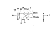
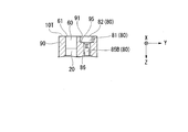
- Modifications 2 and 3) 3A and 3B are diagrams showing a main part of an endoscope according to a modified example of the above-described embodiment, and are a lens unit 60, a light emitting diode 80, and a light shield that constitute the imaging module 10 viewed from the X direction.
- 4 is a cross-sectional view showing a member 90.
- FIG. Modifications 2 and 3 show a structure in which the light emitting diode 80 is arranged next to the lens unit 60.
- the lens unit 60 the light emitting diode 80, and the light shielding member 90 are shown.
- Other members constituting the imaging module 10 shown in FIG. 1 are omitted in this modification.
- a butting portion 95 is provided inside the light guide hole 91 of the light shielding member 90.
- the abutting portion 95 is in contact with the lower surface 86 of the light emitting diode 80 inserted into the light guide hole 91 from the front of the light shielding member 90.
- the abutting portion 95 and the light emitting diode 80 are fixed by a known fixing member such as an adhesive.
- the length (Z direction) of the light guide hole 91 in Modification 2 is shorter than the light guide hole 91 of the first embodiment shown in FIG. Inside the light guide hole 91, the position of the light emitting surface 82 in the Z direction is shifted to the inside of the light guide hole 91 from the end face 10 ⁇ / b> T of the imaging module 10.
- a light guide plate 96 is provided on the light exit surface 82. According to this configuration, the rigid part length L of the imaging module including the light emitting diode 80 can be shortened as in the first modification described above. Further, the light-emitting diode 80 can be protected by the light guide plate 96.
- Modification 3 shown in FIG. 3B is different from Modification 2 in that the light guide plate 96 is not used.
- Other configurations of the third modification are the same as those of the second modification.
- the light exit surface 82 coincides with the imaging surface 61 of the lens unit 60, that is, coincides with the end surface 10 ⁇ / b> T of the imaging module 10.
- the rigid part length L of the imaging module including the light emitting diode 80 can be shortened as in the first modification described above.
- the imaging target can be illuminated over a wide range.
- the structure in which the light emitting diode 80 is arranged next to the lens unit 60 is shown.
- the light emitting diode 80 may be arranged next to the solid-state imaging device 20.
- Modifications 4 and 5 are diagrams showing a main part of an endoscope according to a modified example of the above-described embodiment, in which the solid-state imaging device 20 and the light emitting diode 80 constituting the imaging module 10 viewed from the Z direction are shown.
- FIG. 1 is a diagram showing a main part of an endoscope according to a modified example of the above-described embodiment, in which the solid-state imaging device 20 and the light emitting diode 80 constituting the imaging module 10 viewed from the Z direction are shown.
- 4A and 4B the solid-state imaging device 20 and the light emitting diode 80 are shown. Other members constituting the imaging module 10 shown in FIG. 1 are omitted in this modification.
- 4A and 4B show a wiring WR (WR1, WR2, WR3, WR4, WR5) connected to a plurality of light emitting diodes, and a power supply PW for supplying power to the plurality of light emitting diodes.
- light emitting diodes 80A and 80B are arranged on the left and right sides of the solid-state imaging device 20.
- the two light emitting diodes 80A and 80B are arranged so as to sandwich the solid-state imaging device 20 in the Y direction.
- the power source PW is connected to the first light emitting diode 80A via the wiring WR1.
- the first light emitting diode 80A is connected to the second light emitting diode 80B via the wiring WR2.
- the second light emitting diode 80B is connected to the power source PW via the wiring WR3. That is, the first light-emitting diode 80A and the second light-emitting diode 80B are connected to the power source PW by serial connection.
- light emitting diodes 80A, 80B, 80C, and 80D are arranged on the top, bottom, left, and right of the solid-state imaging device 20.
- the two light emitting diodes 80A and 80B are disposed so as to sandwich the solid-state imaging element 20 in the Y direction
- the two light emitting diodes 80C and 80D are disposed so as to sandwich the solid-state imaging element 20 in the X direction. That is, the periphery of the solid-state imaging device 20 is surrounded by the light emitting diodes 80A, 80B, 80C, and 80D.
- the power source PW is connected to the first light emitting diode 80A via the wiring WR1.
- the first light emitting diode 80A is connected to the second light emitting diode 80B via the wiring WR2.
- the second light emitting diode 80B is connected to the third light emitting diode 80C via the wiring WR3.
- the third light emitting diode 80C is connected to the fourth light emitting diode 80D via the wiring WR4.
- the fourth light emitting diode 80D is connected to the power source PW via the wiring WR5. That is, the light emitting diodes 80A, 80B, 80C, and 80D are connected to the power source PW by serial connection.
- FIG. 5 is a diagram illustrating a main part of an endoscope according to a modification of the above-described embodiment, and is a cross-sectional view illustrating the structure of the imaging module viewed from the X direction.
- the imaging module 10 has a structure in which the outside of the light shielding member 90 is covered with a housing 110.
- the length of the housing 110 in the Z direction is shorter than the rigid part length L.
- a material of the housing 110 it is desirable to select a material having biocompatibility.
- ceramics such as stainless steel, aluminum, titanium, alumina and zirconia are preferably used.
- the inner surface of the housing 110 and the light shielding member 90 are fixed in contact with each other.
- the use of the casing 110 improves resistance to external forces such as bending.
- the gap between the inner surface of the housing 110 and the light shielding member 90 may be filled with resin, and the imaging module 10 may be fixed with the resin.
- the imaging module according to the sixth modification the same effect as that obtained by the above-described embodiment can be obtained, and the imaging module 10 having high strength can be realized.
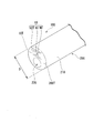
- FIG. 6 is a perspective view showing a main part of the catheter 200 according to the second embodiment of the present invention.
- the same members as those in the first embodiment are denoted by the same reference numerals, and the description thereof is omitted or simplified.
- a catheter 200 illustrated in FIG. 6 is a catheter with an imaging module including the imaging module 10 described above.
- the catheter 200 includes an insulating tube 210 made of, for example, silicon.
- silicon is used as the material of the tube 210, but a flexible material or metal material other than silicon may be used.
- the flexible material include silicon, polyurethane, polyethylene, polytetrafluoroethylene (PTFE, for example, Teflon (registered trademark)), and the like.
- the metal material include titanium, a titanium alloy, and stainless steel.
- not only a flexible material and a metal material but a ceramic material may be used as the material of the tube 210.
- an endoscope 100 including the imaging module 10 according to the first embodiment described above and a channel 220 are provided inside the tube 210. That is, the tube 210 surrounds the imaging module 10. On the end surface 200T of the catheter 200, the opening 220T of the channel 220 is opened, and the end surface 10T of the imaging module 10 is exposed. That is, the end surface 92T of the light guide 92, the end surface of the light shielding member 90, and the imaging surface 61 of the lens unit 60 are exposed on the end surface 200T.
- the diameter D of the feasible catheter 200 is about 2 mm, for example.
- the channel 220 may be used as a lumen or may be used as a working channel.
- a solvent injection lumen that discharges the solvent toward the front of the catheter 200 or a vacuum lumen that removes the liquid existing in front of the catheter 200 can be provided in the tube 210.
- a treatment instrument can be inserted into the channel 220. Examples of treatment tools include various forceps, snares, guide wires, stents, laser treatment tools, and high frequency treatment tools.
- the small-diameter endoscope 100 described in the first embodiment is provided in the catheter 200, the same effect as that obtained by the above-described embodiment is obtained.
- a catheter 200 having both a channel 220 and an imaging module and having a small diameter can be realized.
- SYMBOLS 10 Imaging module, 10T ... End surface, 20 ... Solid-state image sensor, 21 ... Light-receiving surface, 22, 22A, 22B, 22C, 22D ... Imaging terminal, 30 ... Connection body, 31 ... Main body, 31b ... Lower surface, 31t ... Upper surface, 32A, 32B, 32C, 32D ... side terminals, 33A, 33C ... first embedded conductor (embedded conductor), 33B, 33D ... second embedded conductor (embedded conductor), 34B, 34D ... lower surface terminal, 35 ... solder, 40 ... Coaxial cable, 40F ... 1st coaxial cable (coaxial cable), 40S ...
- 2nd coaxial cable (coaxial cable), 41, 41A, 41C ... Internal conductor part, 42 ... Covering part, 43, 43B, 43D ... Sheath conductor part, DESCRIPTION OF SYMBOLS 50 ... Condenser, 60 ... Lens unit, 61 ... Imaging surface, 62 ... Cover member, 70 ... Insulating tube, 80 ... Light emitting diode, 80A ... No. Light emitting diode, 80B ... second light emitting diode, 80C ... third light emitting diode, 80D ... fourth light emitting diode, 81 ... light emitting element, 82 ... light emitting surface, 83 ... light emitting element terminal, 83E ... terminal peripheral portion, 85 ...
- electric power Supply cable 85A ... conductive wire, 85AT ... conductive wire tip, 85AS ... side surface portion, 85B ... outer sheath, 85C ... shield member, 86 ... bottom surface, 87 ... cable reinforcement, 90 ... light shielding member, 91 ... light guide hole, 92: Light guide section, 92T: End face, 93: Light emitting diode insertion hole, 94, 95: Abutting section, 96: Light guide plate, 96T: End face, 100: Endoscope, 110: Housing, 200: Catheter, 200T ... End face, 210 ... Tube, 220 ... Channel, 220T ... Opening, F ... Curved surface, H ... Hard part, K ... Boundary part, L ... Hard part length, PW ... Power source, R ... Rear region, WR, WR , WR2, WR3, WR4, WR5 ... wiring
Landscapes
- Health & Medical Sciences (AREA)
- Life Sciences & Earth Sciences (AREA)
- Surgery (AREA)
- Physics & Mathematics (AREA)
- Engineering & Computer Science (AREA)
- Optics & Photonics (AREA)
- Medical Informatics (AREA)
- General Health & Medical Sciences (AREA)
- Pathology (AREA)
- Nuclear Medicine, Radiotherapy & Molecular Imaging (AREA)
- Biomedical Technology (AREA)
- Heart & Thoracic Surgery (AREA)
- Biophysics (AREA)
- Molecular Biology (AREA)
- Animal Behavior & Ethology (AREA)
- Radiology & Medical Imaging (AREA)
- Public Health (AREA)
- Veterinary Medicine (AREA)
- Multimedia (AREA)
- Signal Processing (AREA)
- Astronomy & Astrophysics (AREA)
- General Physics & Mathematics (AREA)
- Endoscopes (AREA)
- Instruments For Viewing The Inside Of Hollow Bodies (AREA)
Abstract
本発明の撮像モジュールは、光出射面及び発光素子端子を有する平面発光素子と、前記平面発光素子の前記発光素子端子に接続され、前記平面発光素子に電力を供給する電力供給ケーブルと、前記平面発光素子の前記光出射面から出射する光によって照射される照明対象を撮像する固体撮像素子と、前記固体撮像素子に電気的に接続されている同軸ケーブルと、前記固体撮像素子と前記平面発光素子と間に設けられた遮光部材と、前記平面発光素子の前記光出射面から出射する光を前記撮像モジュールの外部に導く導光部と、を備え、前記平面発光素子、前記固体撮像素子、前記遮光部材の一部、及び前記導光部は、硬性部を構成する。
Description
本発明は、撮像モジュール、内視鏡、及びカテーテルに関する。
本願は、2018年2月14日に日本に出願された特願2018-024185号に基づき優先権を主張し、その内容をここに援用する。
本願は、2018年2月14日に日本に出願された特願2018-024185号に基づき優先権を主張し、その内容をここに援用する。
従来、照明用のライトガイドファイババンドルを備えた内視鏡が知られている(例えば、特許文献1参照)。この内視鏡では、固体撮像素子や撮像素子保持筒等により構成される撮像モジュールに干渉しないようにファイババンドルが配置され、ファイババンドルを構成する光ファイバの間の空間に低粘度接着剤が充填されている。内視鏡の後方には、ファイババンドルに光を供給する光源が設けられており、光源から出射された光は、ファイババンドルを通じて、内視鏡の先端に導かれる。
しかしながら、ライトガイドファイババンドルを備えた内視鏡においては、以下の問題点がある。ファイババンドルは剛性を有するため、十分に曲げることができない。このため、ファイババンドルを内視鏡に用いることで、内視鏡の可撓性が低下する。ファイババンドルの曲げによって、光ファイバが折れた場合には、光源からの光をファイババンドルの先端に導くことができない。充分な照度を得るにはファイババンドルを構成する光ファイバの本数を多くする必要があり、この場合にはファイババンドルの断面積が増加し、細径の内視鏡を提供できない。内視鏡の全長に亘ってファイババンドルが配置されるので、内視鏡の投影面内で充分な大きさを有するワーキングチャネルを確保できない。更に、ファイババンドルの材料コスト、組み込みコストが大きく、安価な内視鏡を提供できない。
本発明の一つの態様は、このような従来の事情に鑑みて提案されたものであり、可撓性及び照度が十分に得られる内視鏡を実現できる細径の撮像モジュールと、この撮像モジュールを備える内視鏡と、この撮像モジュールを備えるカテーテルを提供することを目的の一つとする。
上記目的を達成するために、本発明の第1態様に係る撮像モジュールは、光出射面及び発光素子端子を有する平面発光素子と、前記平面発光素子の前記発光素子端子に接続され、前記平面発光素子に電力を供給する電力供給ケーブルと、前記平面発光素子の前記光出射面から出射する光によって照射される照明対象を撮像する固体撮像素子と、前記固体撮像素子に電気的に接続されている同軸ケーブルと、前記固体撮像素子と前記平面発光素子と間に設けられた遮光部材と、前記平面発光素子の前記光出射面から出射する光を前記撮像モジュールの外部に導く導光部と、を備え、前記平面発光素子、前記固体撮像素子、前記遮光部材の一部、及び前記導光部は、硬性部を構成する。
本発明の第1態様に係る撮像モジュールにおいては、前記固体撮像素子と前記同軸ケーブルとの間に位置し、絶縁部材で構成された本体と、前記本体の内部に設けられかつ前記固体撮像素子と前記同軸ケーブルとを電気的に接続する埋め込み導体とを有する接続体を備えてもよい。
本発明の第1態様に係る撮像モジュールにおいては、前記接続体は、前記本体の側面に形成された溝部の内部において前記埋め込み導体が露出する側面端子を備え、前記側面端子に前記同軸ケーブルが電気的に接続されており、前記接続体の後方における前記同軸ケーブルに面する後方領域にて、前記平面発光素子は前記同軸ケーブルに隣り合うように配置されてもよい。
本発明の第1態様に係る撮像モジュールにおいては、前記照明対象からの反射光を前記固体撮像素子の受光面に結像するレンズユニットを備え、前記平面発光素子は、前記レンズユニット又は前記固体撮像素子の隣りに配置されてもよい。
本発明の第1態様に係る撮像モジュールにおいては、前記電力供給ケーブルは、前記発光素子端子に接続される導電線を備え、前記導電線の導電線先端が前記発光素子端子に突き当てられ、前記発光素子端子と前記導電線先端との接触部を覆うように半田が形成されてもよい。
本発明の第1態様に係る撮像モジュールにおいては、前記発光素子端子は、前記発光素子端子の端部に位置する端子外周部を有し、前記導電線は、前記導電線先端から離れた位置にある側面部を有し、前記半田は、前記端子外周部から前記側面部に向けて延びる曲面を形成するように、前記発光素子端子及び前記導電線を覆ってもよい。
本発明の第1態様に係る撮像モジュールにおいては、前記電力供給ケーブルは、前記導電線の外側を覆っているシールド部材を備えてもよい。
本発明の第1態様に係る撮像モジュールにおいては、前記電力供給ケーブルは、極細同軸ケーブルであってもよい。
本発明の第1態様に係る撮像モジュールにおいては、前記発光素子端子及び前記電力供給ケーブルは、ケーブル補強部で被覆されてもよい。
本発明の第1態様に係る撮像モジュールにおいては、前記遮光部材は、遮光性を有する材料で構成されてもよい。
本発明の第1態様に係る撮像モジュールにおいては、前記導光部の端面には、導光板が設けられてもよい。
本発明の第1態様に係る撮像モジュールにおいては、前記導光部の端面は、前記撮像モジュールの端面に一致してもよい。
本発明の第1態様に係る撮像モジュールにおいては、複数の前記平面発光素子を備え、平面視において、複数の前記平面発光素子は、前記固体撮像素子を挟むように配置されてもよい。
本発明の第1態様に係る撮像モジュールにおいては、複数の前記平面発光素子を備え、平面視において、複数の前記平面発光素子は、前記固体撮像素子を囲むように配置されてもよい。
本発明の第1態様に係る撮像モジュールにおいては、前記遮光部材の外部を覆う筐体を備えてもよい。
上記目的を達成するために、本発明の第2態様に係る内視鏡は、第1態様に係る撮像モジュールを備える。
上記目的を達成するために、本発明の第3態様に係るカテーテルは、第1態様に係る撮像モジュールと、前記撮像モジュールを囲む絶縁性のチューブと、前記チューブに設けられたチャネルと、を備える。
以上のように、本発明の上述した態様によれば、可撓性及び照度が十分に得られる内視鏡を実現できる細径の撮像モジュールを提供することができる。また、可撓性及び照度が十分に得られた極細の内視鏡及びカテーテルを提供することができる。
以下、本発明の実施形態について、図面を参照して説明する。
本発明の実施形態を説明する図においては、各構成要素を図面上で認識し得る程度の大きさとするため、各構成要素の寸法及び比率を実際のものとは適宜に異ならせてある。
本発明の実施形態を説明する図においては、各構成要素を図面上で認識し得る程度の大きさとするため、各構成要素の寸法及び比率を実際のものとは適宜に異ならせてある。
(第1実施形態)
(内視鏡100)
図1及び図2は、本発明の第1実施形態に係る内視鏡100の要部を示す図であって、撮像モジュール10の構造を示す断面図である。特に、図1はY方向から見た断面図であり、図2はX方向から見た断面図である。
後述する説明では、Z方向において、接続体30から固体撮像素子20に向かう方向(図1における左側)を「前方」或いは「前側」と称する場合がある。接続体30から同軸ケーブル40に向かう方向(図1における右側)を「後方」或いは「後側」と称する場合がある。
(内視鏡100)
図1及び図2は、本発明の第1実施形態に係る内視鏡100の要部を示す図であって、撮像モジュール10の構造を示す断面図である。特に、図1はY方向から見た断面図であり、図2はX方向から見た断面図である。
後述する説明では、Z方向において、接続体30から固体撮像素子20に向かう方向(図1における左側)を「前方」或いは「前側」と称する場合がある。接続体30から同軸ケーブル40に向かう方向(図1における右側)を「後方」或いは「後側」と称する場合がある。
(撮像モジュール10)
撮像モジュール10は、固体撮像素子20(撮像素子)と、接続体30と、2本の同軸ケーブル40(第1同軸ケーブル40F、第2同軸ケーブル40S)と、コンデンサ50(電子部品)、レンズユニット60と、絶縁チューブ70と、発光ダイオード80と、遮光部材90とを備える。
撮像モジュール10は、固体撮像素子20(撮像素子)と、接続体30と、2本の同軸ケーブル40(第1同軸ケーブル40F、第2同軸ケーブル40S)と、コンデンサ50(電子部品)、レンズユニット60と、絶縁チューブ70と、発光ダイオード80と、遮光部材90とを備える。
(固体撮像素子20)
固体撮像素子20は、接続体30の前方に設けられている。
固体撮像素子20は、固体撮像素子20の上面に位置する受光面21と、固体撮像素子20の下面に設けられた4つの撮像端子22(22A、22B、22C、22D)とを備える。受光面21には、レンズユニット60が搭載されている。撮像端子22は、接続体30の上面31t上に設けられた実装パッド(後述)に接続される端子である。固体撮像素子20としては、例えば、CMOS(相補型金属酸化膜半導体)を好適に用いられる。
撮像モジュール10においては、接続体30を介して、固体撮像素子20が2本の同軸ケーブル40に電気的に接続されている。
固体撮像素子20は、接続体30の前方に設けられている。
固体撮像素子20は、固体撮像素子20の上面に位置する受光面21と、固体撮像素子20の下面に設けられた4つの撮像端子22(22A、22B、22C、22D)とを備える。受光面21には、レンズユニット60が搭載されている。撮像端子22は、接続体30の上面31t上に設けられた実装パッド(後述)に接続される端子である。固体撮像素子20としては、例えば、CMOS(相補型金属酸化膜半導体)を好適に用いられる。
撮像モジュール10においては、接続体30を介して、固体撮像素子20が2本の同軸ケーブル40に電気的に接続されている。
(接続体30)
接続体30は、固体撮像素子20と同軸ケーブル40との間に位置する。
接続体30は、絶縁部材で構成された本体31と、本体31の内部に設けられた埋め込み導体33A、33C(第1埋め込み導体)及び埋め込み導体33B、33D(第2埋め込み導体)とを備える。
本体31の側面には、接続体30が部分的に除去された溝部が形成されている。この溝部の内部には、埋め込み導体33A、33Cの各々が露出する側面端子32A、32C(第1側面端子)と、埋め込み導体33B、33Dの各々が露出する側面端子32B、32D(第2側面端子)とが設けられている。
本体31の下面31bには、埋め込み導体33B、33Dが露出する下面端子34B、34Dが設けられている。
接続体30は、固体撮像素子20と同軸ケーブル40との間に位置する。
接続体30は、絶縁部材で構成された本体31と、本体31の内部に設けられた埋め込み導体33A、33C(第1埋め込み導体)及び埋め込み導体33B、33D(第2埋め込み導体)とを備える。
本体31の側面には、接続体30が部分的に除去された溝部が形成されている。この溝部の内部には、埋め込み導体33A、33Cの各々が露出する側面端子32A、32C(第1側面端子)と、埋め込み導体33B、33Dの各々が露出する側面端子32B、32D(第2側面端子)とが設けられている。
本体31の下面31bには、埋め込み導体33B、33Dが露出する下面端子34B、34Dが設けられている。
埋め込み導体33A、33B、33C、33Dは、接続体30の上面31t上に設けられた実装パッドを介して、各々、撮像端子22A、22B、22C、22Dに電気的に接続されている。
接続体30の上面31tの一辺の長さ(X方向及びY方向)は、2mm以下である。
接続体30の上面31tの一辺の長さ(X方向及びY方向)は、2mm以下である。
(同軸ケーブル40)
図1に示すように、撮像モジュール10は、2本の同軸ケーブル40(40F、40S)を備える。同軸ケーブル40の各々は、内部導体部41(41A、41C)と、被覆部42(絶縁体)と、シース導体部43(43B、43D)とを有する。具体的に、同軸ケーブル40Fは、内部導体部41A及びシース導体部43Bを備える。同軸ケーブル40Sは、内部導体部41C及びシース導体部43Dを備える。
内部導体部41の長さ、シース導体部43の長さ、内部導体部41及びシース導体部43の間に位置する被覆部42の長さは、0.1~1.0mmである。
図1に示すように、撮像モジュール10は、2本の同軸ケーブル40(40F、40S)を備える。同軸ケーブル40の各々は、内部導体部41(41A、41C)と、被覆部42(絶縁体)と、シース導体部43(43B、43D)とを有する。具体的に、同軸ケーブル40Fは、内部導体部41A及びシース導体部43Bを備える。同軸ケーブル40Sは、内部導体部41C及びシース導体部43Dを備える。
内部導体部41の長さ、シース導体部43の長さ、内部導体部41及びシース導体部43の間に位置する被覆部42の長さは、0.1~1.0mmである。
同軸ケーブル40の内部導体部41、被覆部42、及びシース導体部43は、接続体30の溝部内に配置されている。内部導体部41Aは、はんだ付けによって側面端子32Aに電気的に接続されている。シース導体部43Bは、はんだ付けによって側面端子32Bに電気的に接続されている。内部導体部41Cは、はんだ付けによって側面端子32Cに電気的に接続されている。シース導体部43Dは、はんだ付けによって側面端子32Dに電気的に接続されている。
上述した接続構造により、固体撮像素子20の撮像端子22Aは、埋め込み導体33Aを介して、内部導体部41Aと電気的に接続されている。固体撮像素子20の撮像端子22Bは、埋め込み導体33Bを介して、シース導体部43Bと電気的に接続されている。
固体撮像素子20の撮像端子22Cは、埋め込み導体33Cを介して、内部導体部41Cと電気的に接続されている。固体撮像素子20の撮像端子22Dは、埋め込み導体33Dを介して、シース導体部43Dと電気的に接続されている。
固体撮像素子20の撮像端子22Cは、埋め込み導体33Cを介して、内部導体部41Cと電気的に接続されている。固体撮像素子20の撮像端子22Dは、埋め込み導体33Dを介して、シース導体部43Dと電気的に接続されている。
(コンデンサ50)
コンデンサ50は、実装パッドを介して接続体30の下面31bに設けられている。コンデンサ50の外部端子は、下面端子34B、34Dに接続されている。なお、接続体30の下面31b上には、樹脂層が設けられており、下面端子34B、34Dの間における短絡が防止されている。
コンデンサ50は、実装パッドを介して接続体30の下面31bに設けられている。コンデンサ50の外部端子は、下面端子34B、34Dに接続されている。なお、接続体30の下面31b上には、樹脂層が設けられており、下面端子34B、34Dの間における短絡が防止されている。
(レンズユニット60)
レンズユニット60は、円筒状の鏡筒(不図示)内に、対物レンズ(図示略)が組み込まれた構成を有する。このレンズユニット60の光軸は、固体撮像素子20の受光面21に位置合わせされている。鏡筒の軸線方向における一端は、カバー部材62に固定されている。レンズユニット60は、レンズユニット60の前側に位置する撮像面61から入射して鏡筒内のレンズを介して導かれた光を、固体撮像素子20の受光面21に結像させる。
レンズユニット60は、円筒状の鏡筒(不図示)内に、対物レンズ(図示略)が組み込まれた構成を有する。このレンズユニット60の光軸は、固体撮像素子20の受光面21に位置合わせされている。鏡筒の軸線方向における一端は、カバー部材62に固定されている。レンズユニット60は、レンズユニット60の前側に位置する撮像面61から入射して鏡筒内のレンズを介して導かれた光を、固体撮像素子20の受光面21に結像させる。
(絶縁チューブ70)
絶縁チューブ70は、電気絶縁性を有する樹脂製のチューブである。絶縁チューブ70としては、熱収縮チューブが用いられる。絶縁チューブ70の材料としては、例えば、ポリイミド樹脂、シリコーン樹脂、ポリエチレンテレフタレート(PET)、ナイロン、ポリエチレンまたはポリプロピレン等のポリオレフィン系、及びポリテトラフルオロエチレン(PTFE)等のフッ素系樹脂等が用いられる。
絶縁チューブ70は、電気絶縁性を有する樹脂製のチューブである。絶縁チューブ70としては、熱収縮チューブが用いられる。絶縁チューブ70の材料としては、例えば、ポリイミド樹脂、シリコーン樹脂、ポリエチレンテレフタレート(PET)、ナイロン、ポリエチレンまたはポリプロピレン等のポリオレフィン系、及びポリテトラフルオロエチレン(PTFE)等のフッ素系樹脂等が用いられる。
絶縁チューブ70は、少なくとも、接続体30と、接続体30に接続される同軸ケーブル40の一部とを覆っている。接続体30にコンデンサ50が接続されている本実施形態では、絶縁チューブ70は、接続体30と、同軸ケーブル40の一部と、コンデンサ50とを一括して覆っている。ここで、同軸ケーブル40の一部とは、内部導体部41、被覆部42、及びシース導体部43が形成されている領域(露出領域)だけでなく、接続体30の近くに位置する外被(シース導体部43を覆っている部分)を含む領域を意味する。
本実施形態では、図1に示すようにコンデンサ50の端部から外側(右側)に向けて突出するように、絶縁チューブ70が同軸ケーブル40を覆っている。この構造により、絶縁チューブ70は、接続体30、同軸ケーブル40、及びコンデンサ50を保護するとともに、高い絶縁性を実現することができる。
(発光ダイオード80)
発光ダイオード80は、厚さ0.25mm程度の平板の発光素子81(平面発光素子)と、発光素子81の前方に位置する平面である光出射面82と、発光素子81の後方に位置する面(光出射面82とは反対側の面)に設けられた発光素子端子83とを備える。発光素子端子83は、後述する電力供給ケーブル85と電気的に接続されている。
発光ダイオード80は、厚さ0.25mm程度の平板の発光素子81(平面発光素子)と、発光素子81の前方に位置する平面である光出射面82と、発光素子81の後方に位置する面(光出射面82とは反対側の面)に設けられた発光素子端子83とを備える。発光素子端子83は、後述する電力供給ケーブル85と電気的に接続されている。
本実施形態において、発光ダイオード80として、表面実装型発光ダイオードが適用されている。これにより、直進性を有する光を光出射面82から出射することができ、かつ、充分な照度を確保することができる。
なお、表面実装型発光ダイオードに限らず、良好な光の直進性が得られれば、他の構造を有する発光ダイオードが本発明に適用されてもよい。
なお、表面実装型発光ダイオードに限らず、良好な光の直進性が得られれば、他の構造を有する発光ダイオードが本発明に適用されてもよい。
発光ダイオード80は、接続体30の後方において、コンデンサ50及び同軸ケーブル40に面する後方領域Rに配置されている。より具体的に、発光ダイオード80は、同軸ケーブル40に隣り合うように、発光ダイオード80の光出射面82の一部とコンデンサ50とが互いに対向するように、配置されている。換言すると、接続体30の後方において、同軸ケーブル40が配置されていない後方領域Rに、発光ダイオード80が配置されている。
なお、本実施形態では、コンデンサ50が接続体30の下面31bに設けられた例を説明しているが、コンデンサ50が設けられていない構成では、光出射面82の一部と下面31bとが互いに対向するように、発光ダイオード80は、後方領域Rに配置される。
電力供給ケーブル85は、導電線85Aと、導電線85Aを覆う外被85Bと、外被85Bを覆うシールド部材85Cとを備える。導電線85Aは、不図示の電源から電力を発光素子端子83に供給する。外被85Bは、導電線85Aの表面に絶縁性を付与する絶縁被覆である。シールド部材85Cは、外被85Bを覆っており、即ち、導電線85Aの外側を覆っている。シールド部材85Cは、金属メッシュ等の金属部材で形成されており、導電線85Aに供給される電力に起因するノイズが同軸ケーブル40に影響を及ぼすことを抑制する。シールド部材85Cの外周は、絶縁材料で覆われている。なお、電力供給ケーブル85は、極細同軸ケーブルであってもよい。
電力供給ケーブル85は、発光ダイオード80に電圧を印加する2本のケーブルで構成されている。2本のケーブルの各々が、導電線85Aと外被85Bとを備える。シールド部材85Cは、2本のケーブルの各々の外被85Bを覆う構成を有してもよいし、2本のケーブルの2つの外被85Bを一括して覆う構成を有してもよい。
なお、シールド部材85Cを必ずしも設ける必要はなく、シールド部材85Cを備えない構造が採用されてもよい。
なお、シールド部材85Cを必ずしも設ける必要はなく、シールド部材85Cを備えない構造が採用されてもよい。
電力供給ケーブル85においては、外被85Bを除去することで導電線85Aが露出しており、露出した導電線85Aは、半田35を用いて、発光素子端子83に突き当ててはんだ付けされている。具体的に、導電線85Aの導電線先端85ATが発光素子端子83に突き当てられており、半田35は、発光素子端子83と導電線先端85ATとの接触部を覆うように形成されている。
発光素子端子83上に形成された半田35においては、半田35の表面に曲面F(フィレット形状)が形成されていることが好ましい。
曲面Fの形状は、発光素子端子83の面に供給される半田35の量に応じて適宜調整可能である。曲面Fの形状は、図2に示す形状に限定されない。
曲面Fの形状は、発光素子端子83の面に供給される半田35の量に応じて適宜調整可能である。曲面Fの形状は、図2に示す形状に限定されない。
特に、発光素子端子83は、発光素子端子83の端部(導電線85Aから離れた位置)に位置する端子外周部83Eを有している。導電線85Aは、導電線先端85ATから離れた位置にある側面部85ASを有している。半田35は、端子外周部83Eから側面部85ASに向けて延びる曲面Fを形成するように、発光素子端子83及び導電線85Aを覆っている。ここで、図2における側面部85ASのZ方向における位置は、発光素子端子83から離れた位置であり、導電線85Aと外被85Bとの間の境界部Kの近くにある。或いは、側面部85ASは、導電線85Aと外被85Bとの間の境界部Kを覆ってもよい。
発光素子端子83及び電力供給ケーブル85は、後述する発光ダイオード挿通孔93の内部で、ケーブル補強部87により固定されている。ケーブル補強部87は、発光ダイオード80の下面において、発光素子端子83、半田35、及び電力供給ケーブル85を覆っている。
これにより、発光素子端子83と電力供給ケーブル85との間の接続強度が増加する。
これにより、発光素子端子83と電力供給ケーブル85との間の接続強度が増加する。
電力供給ケーブル85は、不図示の電源に接続されている。電源から出力される電力は、電力供給ケーブル85を通じて、発光ダイオード80に供給される。換言すると、同軸ケーブル40とは異なるケーブルを通じて、電力が発光ダイオード80に供給される。電力供給ケーブル85は、従来の内視鏡において用いられるファイババンドルを構成する光ファイバよりも柔らかく、可撓性を有する。
(遮光部材90)
遮光部材90は、固体撮像素子20と発光ダイオード80との間に設けられており、特に、本実施形態では、撮像モジュール10を構成する部材の全体、即ち、固体撮像素子20、接続体30、同軸ケーブル40、コンデンサ50、レンズユニット60、絶縁チューブ70、及び発光ダイオード80を覆っている。即ち、遮光部材90は、撮像モジュール10を構成する部材の全体を一体的に保持する。
図2に示す例では、Z方向における遮光部材90の長さは、後述する硬性部Hの長さ(硬性部長L)に設定されている。遮光部材90の長さは、図2に示す例に限定されず、硬性部長Lよりも短くてもよい。
遮光部材90は、固体撮像素子20と発光ダイオード80との間に設けられており、特に、本実施形態では、撮像モジュール10を構成する部材の全体、即ち、固体撮像素子20、接続体30、同軸ケーブル40、コンデンサ50、レンズユニット60、絶縁チューブ70、及び発光ダイオード80を覆っている。即ち、遮光部材90は、撮像モジュール10を構成する部材の全体を一体的に保持する。
図2に示す例では、Z方向における遮光部材90の長さは、後述する硬性部Hの長さ(硬性部長L)に設定されている。遮光部材90の長さは、図2に示す例に限定されず、硬性部長Lよりも短くてもよい。
遮光部材90には、2つの貫通孔、即ち、導光孔91及び発光ダイオード挿通孔93が設けられている。さらに、発光ダイオード挿通孔93の内部には、発光ダイオード挿通孔93と導光孔91との間に形成された段差、即ち、突き当て部94が設けられている。この突き当て部94は、後方領域Rに位置する。
導光孔91の内部には、光出射面82の一部が露出している。導光孔91の内部にはZ方向に延在する導光部92が設けられている。導光部92は、発光ダイオード80の光出射面82から出射する光を撮像モジュール10の外部に導く。
導光部92は、例えば、流動性を有する液体樹脂を硬化させた透明樹脂であり、導光孔91の内部に固定されており、屈曲性を有しない。また、導光部92の材料は樹脂に限定されずガラスや光ファイバであってもよい。即ち、導光孔91及び導光部92は、光路として機能する。
なお、導光孔91の内部は空間であってもよい。即ち、導光部92は、導光孔91の内部に設けられた導光部材でもよいし、空間であってもよい。ただし、光出射面82から出射される光の直進性を得るために、導光孔91の内部に導光部92を設けることが好ましい。
導光部92は、例えば、流動性を有する液体樹脂を硬化させた透明樹脂であり、導光孔91の内部に固定されており、屈曲性を有しない。また、導光部92の材料は樹脂に限定されずガラスや光ファイバであってもよい。即ち、導光孔91及び導光部92は、光路として機能する。
なお、導光孔91の内部は空間であってもよい。即ち、導光部92は、導光孔91の内部に設けられた導光部材でもよいし、空間であってもよい。ただし、光出射面82から出射される光の直進性を得るために、導光孔91の内部に導光部92を設けることが好ましい。
導光孔91の内表面には、光を反射する反射面が形成されてもよい。
また、導光孔91は、遮光部材90に埋め込まれたステンレス(SUS)等の金属管であってもよい。この場合、金属管は遮光部材として機能し、この金属管は樹脂等によって、レンズユニット60、固体撮像素子20、及び接続体30の隣りに固定される。
また、導光孔91は、遮光部材90に埋め込まれたステンレス(SUS)等の金属管であってもよい。この場合、金属管は遮光部材として機能し、この金属管は樹脂等によって、レンズユニット60、固体撮像素子20、及び接続体30の隣りに固定される。
導光部92の前方における端面92Tには、平板状の導光板96が設けられている。Z方向において、導光板96の端面96Tは、レンズユニット60の撮像面61の一致しており、即ち、撮像モジュール10の端面10Tに一致している。
導光板96は、光透過性の高い透明樹脂で形成されており、例えば、ポリカーボネート等で構成された樹脂板である。或いは、導光板96は、導光孔91の一部と端面92Tとで囲まれた凹部に液状の接着剤が充填された後に、硬化された部材であってもよい。
導光板96は、光透過性の高い透明樹脂で形成されており、例えば、ポリカーボネート等で構成された樹脂板である。或いは、導光板96は、導光孔91の一部と端面92Tとで囲まれた凹部に液状の接着剤が充填された後に、硬化された部材であってもよい。
導光板96は、発光ダイオード80を保護する保護カバー(保護部材)として機能してもよい。また、導光板96は、導光部92によって導かれた光を屈折させるレンズ(光学部材)として機能してもよい。また、導光板96は、導光部92によって導かれた光を導光板96の外部に向けて拡散させる光拡散板(光学部材)として機能してもよい。
本実施形態に係る撮像モジュール10が生体を観察するような内視鏡に適用される場合、導光板96は、生体の体液等が撮像モジュール10に付着することを防止する付着防止部材として機能してもよい。また、導光板96は、生体適合性を有する材料で形成されてもよい。
発光ダイオード挿通孔93は、遮光部材90の内部に発光ダイオード80を取り付ける際に、遮光部材90の後方から内部に向けて発光ダイオード80が通る孔である。発光ダイオード挿通孔93の内部において、発光ダイオード80は、突き当て部94に接触し、接着剤等の公知の固定部材により固定されている。このような固定構造では、光出射面82の一部と、突き当て部94とが接触し、固定されている。
符号Hは、撮像モジュール10において屈曲しない部分、即ち、硬性部Hである。
硬性部Hは、少なくとも、発光ダイオード80、固体撮像素子20、遮光部材90の一部によって構成されていればよい。本実施形態では、発光ダイオード80、レンズユニット60、固体撮像素子20、遮光部材90の一部、接続体30、及び同軸ケーブル40の一部によって硬性部Hが構成されている。硬性部Hの長さ、即ち、硬性部長Lは、例えば、約5mmである。
遮光部材90を構成する材料としては、エポキシ樹脂、アクリル樹脂、ウレタン樹脂等の公知の遮光性を有する樹脂が採用される。また、公知の樹脂にカーボンブラックが添加された材料を用いて遮光部材90が形成されてもよい。
硬性部Hは、少なくとも、発光ダイオード80、固体撮像素子20、遮光部材90の一部によって構成されていればよい。本実施形態では、発光ダイオード80、レンズユニット60、固体撮像素子20、遮光部材90の一部、接続体30、及び同軸ケーブル40の一部によって硬性部Hが構成されている。硬性部Hの長さ、即ち、硬性部長Lは、例えば、約5mmである。
遮光部材90を構成する材料としては、エポキシ樹脂、アクリル樹脂、ウレタン樹脂等の公知の遮光性を有する樹脂が採用される。また、公知の樹脂にカーボンブラックが添加された材料を用いて遮光部材90が形成されてもよい。
本実施形態では、固体撮像素子20、レンズユニット60、接続体30、及び発光ダイオード80を覆うように、遮光部材90が設けられているが、本発明は、遮光部材90の構造を限定しない。固体撮像素子20及びレンズユニット60の周囲に遮光部材90を設けて、発光ダイオード80からの出射光が固体撮像素子20及びレンズユニット60に入射することを防止してもよい。遮光部材90は、遮光機能を有するだけでなく、後述する絶縁チューブ70の機能を有してもよい。この場合、絶縁チューブ70を設ける必要がなくなる。
発光ダイオード80から出射された光は、導光部92を通じて、撮像モジュール10の外部に出射する。また、遮光部材90によって、発光ダイオード80からの出射光が固体撮像素子20に入射することが防止されている。
次に、以上のように構成された撮像モジュール10を備えた内視鏡100の作用について説明する。
電力供給ケーブル85を通じて電力が発光ダイオード80に供給されると、発光ダイオード80は発光し、発光ダイオード80から発光した光は、導光部92を通じて撮像モジュール10の外部に出射する。この光は、内視鏡100によって観察される照明対象を照明し、照明対象からの反射光(像)は、レンズユニット60の撮像面61に入射する。レンズユニット60に入射した光(像)は、対物レンズによって固体撮像素子20の受光面21に結像される。これによって、固体撮像素子20は、照明対象を撮像し、得られた画像を電気信号として出力する。固体撮像素子20から出力された信号は、同軸ケーブル40を通じて、撮像モジュール10の外部に設けられた制御装置によって受信される。
電力供給ケーブル85を通じて電力が発光ダイオード80に供給されると、発光ダイオード80は発光し、発光ダイオード80から発光した光は、導光部92を通じて撮像モジュール10の外部に出射する。この光は、内視鏡100によって観察される照明対象を照明し、照明対象からの反射光(像)は、レンズユニット60の撮像面61に入射する。レンズユニット60に入射した光(像)は、対物レンズによって固体撮像素子20の受光面21に結像される。これによって、固体撮像素子20は、照明対象を撮像し、得られた画像を電気信号として出力する。固体撮像素子20から出力された信号は、同軸ケーブル40を通じて、撮像モジュール10の外部に設けられた制御装置によって受信される。
上述した第1実施形態に係る撮像モジュール10によれば、電力供給ケーブル85は、光ファイバよりも柔らかく、十分な可撓性を有するため、光ファイバで構成されるファイババンドルよりも、可撓性に優れた撮像モジュールを実現することができる。また、発光ダイオード80から発光した光を撮像モジュール10の外部に出射することができるため、十分な照度が得られる内視鏡100を実現することができる。
電力供給ケーブル85は、従来のようなファイババンドルに比べて細いため、細径の撮像モジュール10を実現することができ、即ち、細径の内視鏡100を実現することができる。
電力供給ケーブル85は、従来のようなファイババンドルに比べて細いため、細径の撮像モジュール10を実現することができ、即ち、細径の内視鏡100を実現することができる。
本実施形態では、接続体30の本体31の側面に形成された溝部の内部に設けられた側面端子32A、32B、32C、32Dに、同軸ケーブル40F、40Sが接続されている。この構造により、接続体30の後方に、同軸ケーブルが配置されていない後方領域Rを得ることができ、後方領域Rにおいて発光ダイオード80を配置することができる。
このため、撮像モジュール10を構成する部材の配置レイアウトにおいて、発光ダイオード80を配置する位置として後方領域Rを有効的に利用することができる。即ち、接続体30の後方に同軸ケーブルが配置されている構造と比較して、Z方向に鉛直な方向(図2の場合ではY方向)において同軸ケーブル40F、40Sに近づくように、発光ダイオード80を配置することができる。従って、細径の撮像モジュール10を実現することができ、即ち、細径の内視鏡100を実現することができる。
発光ダイオード80として、Z方向における厚さの薄い平板の表面実装型発光ダイオードが撮像モジュール10に適用されているので、硬性部長Lを短くすることができる。
また、硬性部Hにおいて、導光部92は導光孔91の内部に固定されており、導光部92の屈曲が防止されている。このため、屈曲に起因して導光部92が破損することがない。
また、硬性部Hにおいて、導光部92は導光孔91の内部に固定されており、導光部92の屈曲が防止されている。このため、屈曲に起因して導光部92が破損することがない。
発光ダイオード80と電力供給ケーブル85との接続構造において、表面実装型発光ダイオードに導電線85Aを有する電力供給ケーブル85を適用することで、材料コストおよび組立コストを低く抑えることができる。
電力供給ケーブル85は、ファイババンドルに比べて細いため、電力供給ケーブル85を備える撮像モジュール10を内視鏡又はカテーテルに適用することで、投影面内で充分な大きさを有するワーキングチャネルを確保することができる。
電力供給ケーブル85は、シールド部材85Cを備えるので、導電線85Aに供給される電力に起因するノイズが同軸ケーブル40に影響を及ぼすことを抑制することができる。
電力供給ケーブル85は、ファイババンドルに比べて細いため、電力供給ケーブル85を備える撮像モジュール10を内視鏡又はカテーテルに適用することで、投影面内で充分な大きさを有するワーキングチャネルを確保することができる。
電力供給ケーブル85は、シールド部材85Cを備えるので、導電線85Aに供給される電力に起因するノイズが同軸ケーブル40に影響を及ぼすことを抑制することができる。
半田35に曲面Fを形成することで、半田35の表面積が増加し、発光ダイオード80の放熱性が向上する。特に、樹脂の熱伝導率は0.5W/mK程度であり、これに対して、はんだ及び導電線の熱伝導率は10W/mK以上である。発光ダイオードが樹脂等で覆われた従来の構造では、発光ダイオードからの発熱が、樹脂内部に留まり、放熱し難い。
これに対し、本実施形態に係る撮像モジュール10によれば、樹脂よりも熱伝導率が高い半田35の表面積が増加することで、従来よりも、優れた放熱性が得られる。
これに対し、本実施形態に係る撮像モジュール10によれば、樹脂よりも熱伝導率が高い半田35の表面積が増加することで、従来よりも、優れた放熱性が得られる。
更に、発光素子端子83に導電線85Aを直接的に接続することで、発光ダイオード80の放熱を充分に行うことができる。また、半田35に曲面Fを形成することで、また、発光素子端子83と導電線85Aとの間の電気的接続の信頼性が向上する。
導電線85Aの導電線先端85ATを発光素子端子83に突き当て、導電線85Aと発光素子端子83とがはんだ付けされているので、はんだ付けされる部分の面積が小さくなり、細径の撮像モジュール10の実現に寄与する。
例えば、導電線が折り曲げられた屈曲部を発光素子端子にはんだ付けする場合では、はんだ付けされる部分の面積が大きくなってしまうが、本実施形態では、半田付けされる面積を小さくすることができる。
例えば、導電線が折り曲げられた屈曲部を発光素子端子にはんだ付けする場合では、はんだ付けされる部分の面積が大きくなってしまうが、本実施形態では、半田付けされる面積を小さくすることができる。
発光ダイオード80と電力供給ケーブル85との接続構造においては、発光ダイオード80の発光素子端子83と電力供給ケーブル85の導電線85Aとが確実に接続されているか否か(接続状態)を確認する必要がある。この場合、発光素子端子83を観察し、発光素子端子83において半田35が曲面Fを有するか否かを判断することで、発光素子端子83と導電線85Aとの接続状態を容易に確認することができる。
(第1実施形態の変形例)
次に、上述した第1実施形態の変形例について説明する。
以下に述べる変形例では、第1実施形態と同一部材には同一符号を付して、その説明は省略または簡略化する。
次に、上述した第1実施形態の変形例について説明する。
以下に述べる変形例では、第1実施形態と同一部材には同一符号を付して、その説明は省略または簡略化する。
(変形例1)
上述した実施形態では、接続体30の溝部に露出する側面端子32A、32B、32C、32Dに同軸ケーブル40が電気的に接続された構造を有する接続体30について説明したが、本発明は、接続体30の構造を限定しない。
上述した実施形態では、接続体30の溝部に露出する側面端子32A、32B、32C、32Dに同軸ケーブル40が電気的に接続された構造を有する接続体30について説明したが、本発明は、接続体30の構造を限定しない。
例えば、接続体30の下面31bに埋め込み導体33A、33B、33C、33Dが露出する露出端子を設け、この露出端子に同軸ケーブル40が電気的に接続されてもよい。
この場合、後方領域Rが形成されない。発光ダイオード80は、X方向やY方向において、固体撮像素子20、接続体30、及び同軸ケーブル40のうちいずれかに隣り合うように配置される。
この場合、後方領域Rが形成されない。発光ダイオード80は、X方向やY方向において、固体撮像素子20、接続体30、及び同軸ケーブル40のうちいずれかに隣り合うように配置される。
この構成では、接続体の内部の配線構造が簡素になり、接続体のZ方向における長さを短くすることができる。従って、発光ダイオード80を備えた撮像モジュールの硬性部長Lを短くすることができる。
また、接続体30が省かれた構造、即ち、固体撮像素子20と同軸ケーブル40とを直接的に接続された構造が採用されてもよい。この場合、発光ダイオード80は、X方向やY方向において、固体撮像素子20及び同軸ケーブル40のうちいずれかに隣り合うように配置される。上記と同様に、発光ダイオード80を備えた撮像モジュールの硬性部長Lを短くすることができる。以下に述べる変形例2、3では、Y方向において発光ダイオード80がレンズユニット60に隣り合う構造について説明する。
(変形例2、3)
図3A及び図3Bは、上述した実施形態の変形例に係る内視鏡の要部を示す図であって、X方向から見た撮像モジュール10を構成するレンズユニット60、発光ダイオード80、及び遮光部材90を示す断面図である。
変形例2、3は、発光ダイオード80がレンズユニット60の隣りに配置された構造を示している。
図3A及び図3Bは、上述した実施形態の変形例に係る内視鏡の要部を示す図であって、X方向から見た撮像モジュール10を構成するレンズユニット60、発光ダイオード80、及び遮光部材90を示す断面図である。
変形例2、3は、発光ダイオード80がレンズユニット60の隣りに配置された構造を示している。
図3A及び図3Bにおいては、レンズユニット60、発光ダイオード80、及び遮光部材90が示されている。図1において示した撮像モジュール10を構成する他の部材は、本変形例では省略されている。
図3Aに示す変形例2では、遮光部材90の導光孔91の内部に突き当て部95が設けられている。突き当て部95には、遮光部材90の前方から導光孔91の内部に挿入された発光ダイオード80の下面86が接触している。突き当て部95及び発光ダイオード80は、接着剤等の公知の固定部材により固定されている。
変形例2における導光孔91の長さ(Z方向)は、図2に示す第1実施形態の導光孔91よりも短い。導光孔91の内部において、光出射面82のZ方向の位置は、撮像モジュール10の端面10Tよりも導光孔91の内側にずれている。
光出射面82上には、導光板96が設けられている。この構成によれば、上述した変形例1と同様に、発光ダイオード80を備えた撮像モジュールの硬性部長Lを短くすることができる。また、導光板96により、発光ダイオード80を保護することができる。
図3Bに示す変形例3は、導光板96が用いられていない点で、変形例2とは異なる。変形例3のその他の構成は、変形例2と同じである。
Z方向において、光出射面82は、レンズユニット60の撮像面61の一致しており、即ち、撮像モジュール10の端面10Tに一致している。
この構成によれば、上述した変形例1と同様に、発光ダイオード80を備えた撮像モジュールの硬性部長Lを短くすることができる。また、光出射面82から広い角度で光が出射するので、撮像対象を広範囲で照明することができる。
Z方向において、光出射面82は、レンズユニット60の撮像面61の一致しており、即ち、撮像モジュール10の端面10Tに一致している。
この構成によれば、上述した変形例1と同様に、発光ダイオード80を備えた撮像モジュールの硬性部長Lを短くすることができる。また、光出射面82から広い角度で光が出射するので、撮像対象を広範囲で照明することができる。
なお、変形例2、3では、発光ダイオード80がレンズユニット60の隣りに配置された構造を示したが、発光ダイオード80は、固体撮像素子20の隣りに配置されてもよい。
(変形例4、5)
図4A及び図4Bは、上述した実施形態の変形例に係る内視鏡の要部を示す図であって、Z方向から見た撮像モジュール10を構成する固体撮像素子20と発光ダイオード80とを示す平面図である。
図4A及び図4Bは、上述した実施形態の変形例に係る内視鏡の要部を示す図であって、Z方向から見た撮像モジュール10を構成する固体撮像素子20と発光ダイオード80とを示す平面図である。
図4A及び図4Bにおいては、固体撮像素子20及び発光ダイオード80が示されている。図1において示した撮像モジュール10を構成する他の部材は、本変形例では省略されている。
なお、図4A及び図4Bにおいては、複数の発光ダイオードに接続される配線WR(WR1、WR2、WR3、WR4、WR5)と、複数の発光ダイオードに電力を供給する電源PWが示されている。
なお、図4A及び図4Bにおいては、複数の発光ダイオードに接続される配線WR(WR1、WR2、WR3、WR4、WR5)と、複数の発光ダイオードに電力を供給する電源PWが示されている。
図4Aに示す変形例4では、固体撮像素子20の左右に発光ダイオード80A、80Bが配置されている。換言すると、Y方向において固体撮像素子20を挟むように2つの発光ダイオード80A、80Bが配置されている。
電源PWは、配線WR1を介して、第1発光ダイオード80Aに接続されている。第1発光ダイオード80Aは、配線WR2を介して、第2発光ダイオード80Bに接続されている。第2発光ダイオード80Bは、配線WR3を介して、電源PWに接続されている。
即ち、第1発光ダイオード80A及び第2発光ダイオード80Bは、直列接続により、電源PWに接続されている。
即ち、第1発光ダイオード80A及び第2発光ダイオード80Bは、直列接続により、電源PWに接続されている。
この構成によれば、図2に示すように一つの発光ダイオード80が撮像モジュール10に設けられた構造よりも、より多くの光量を撮像モジュール10に供給することができる。この構成を内視鏡100に適用することで、より明るく撮像対象を照明することができる。また、第1発光ダイオード80A及び第2発光ダイオード80Bは、直列接続により、電源PWに接続されているため、並列接続に比べて、配線の本数を削減することができる。
図4Bに示す変形例5では、固体撮像素子20の上下左右に発光ダイオード80A、80B、80C、80Dが配置されている。換言すると、Y方向において固体撮像素子20を挟むように2つの発光ダイオード80A、80Bが配置され、X方向において固体撮像素子20を挟むように2つの発光ダイオード80C、80Dが配置されている。即ち、固体撮像素子20の周囲が発光ダイオード80A、80B、80C、80Dで囲まれている。
電源PWは、配線WR1を介して、第1発光ダイオード80Aに接続されている。第1発光ダイオード80Aは、配線WR2を介して、第2発光ダイオード80Bに接続されている。第2発光ダイオード80Bは、配線WR3を介して、第3発光ダイオード80Cに接続されている。第3発光ダイオード80Cは、配線WR4を介して、第4発光ダイオード80Dに接続されている。第4発光ダイオード80Dは、配線WR5介して、電源PWに接続されている。即ち、発光ダイオード80A、80B、80C、80Dは、直列接続により、電源PWに接続されている。
この構成によれば、図4Aに示すように2つの発光ダイオード80A、80Bが撮像モジュール10に設けられた構造よりも、より多くの光量を撮像モジュール10に供給することができる。この構成を内視鏡100に適用することで、より明るく撮像対象を照明することができる。また、発光ダイオード80A、80B、80C、80Dは、直列接続により、電源PWに接続されているため、並列接続に比べて、配線の本数を削減することができる。
(変形例6)
図5は、上述した実施形態の変形例に係る内視鏡の要部を示す図であって、X方向から見た撮像モジュールの構造を示す断面図である。
図5に示すように、撮像モジュール10は、遮光部材90の外部が筐体110で覆われた構造を有する。Z方向における筐体110の長さは、硬性部長Lよりも短い。筐体110の材質としては、生体適合性を有している材料を選択することが望ましい。例えば、ステンレス鋼、アルミニウム、チタン、アルミナやジルコニア等のセラミックが好適に用いられる。
図5は、上述した実施形態の変形例に係る内視鏡の要部を示す図であって、X方向から見た撮像モジュールの構造を示す断面図である。
図5に示すように、撮像モジュール10は、遮光部材90の外部が筐体110で覆われた構造を有する。Z方向における筐体110の長さは、硬性部長Lよりも短い。筐体110の材質としては、生体適合性を有している材料を選択することが望ましい。例えば、ステンレス鋼、アルミニウム、チタン、アルミナやジルコニア等のセラミックが好適に用いられる。
筐体110の内部においては、筐体110の内面と遮光部材90とが接触して固定されている。このような構成においては、筐体110を用いたことによって、曲げ等の外力に対する耐性が向上する。また、筐体110の内面と遮光部材90との間の隙間に樹脂を充填し、樹脂によって撮像モジュール10を固定してもよい。
本変形例6に係る撮像モジュールによれば、上述した実施形態によって得られる効果と同様の効果が得られると共に、高い強度を有する撮像モジュール10を実現することができる。
(第2実施形態)
(カテーテル200)
図6は、本発明の第2実施形態に係るカテーテル200の要部を示す斜視図である。図6において、第1実施形態と同一部材には同一符号を付して、その説明は省略または簡略化する。
(カテーテル200)
図6は、本発明の第2実施形態に係るカテーテル200の要部を示す斜視図である。図6において、第1実施形態と同一部材には同一符号を付して、その説明は省略または簡略化する。
図6に示すカテーテル200は、上述した撮像モジュール10を備えた撮像モジュール付きカテーテルである。
カテーテル200は、例えば、シリコン等で形成された絶縁性のチューブ210を備えている。本実施形態では、チューブ210の材料としてシリコンを挙げたが、シリコン以外の可撓性材料や金属材料が用いられてもよい。
例えば、可撓性材料としては、シリコン、ポリウレタン、ポリエチレン、ポリテトラフルオロエチレン(PTFE、例えば、テフロン(登録商標))等が挙げられる。金属材料としては、チタニウム、チタニウム合金、ステンレス鋼等が挙げられる。また、可撓性材料や金属材料に限らず、セラミックス材料がチューブ210の材料として用いられてもよい。
カテーテル200は、例えば、シリコン等で形成された絶縁性のチューブ210を備えている。本実施形態では、チューブ210の材料としてシリコンを挙げたが、シリコン以外の可撓性材料や金属材料が用いられてもよい。
例えば、可撓性材料としては、シリコン、ポリウレタン、ポリエチレン、ポリテトラフルオロエチレン(PTFE、例えば、テフロン(登録商標))等が挙げられる。金属材料としては、チタニウム、チタニウム合金、ステンレス鋼等が挙げられる。また、可撓性材料や金属材料に限らず、セラミックス材料がチューブ210の材料として用いられてもよい。
チューブ210の内部には、上述した第1実施形態に係る撮像モジュール10を備える内視鏡100と、チャネル220とが設けられている。即ち、チューブ210は、撮像モジュール10を囲っている。
カテーテル200の端面200Tにおいては、チャネル220の開口部220Tが開口し、撮像モジュール10の端面10Tが露出している。即ち、端面200Tには、導光部92の端面92T、遮光部材90の端面、及びレンズユニット60の撮像面61が露出している。本実施形態において、実現可能なカテーテル200の直径Dは、例えば、約2mmである。
カテーテル200の端面200Tにおいては、チャネル220の開口部220Tが開口し、撮像モジュール10の端面10Tが露出している。即ち、端面200Tには、導光部92の端面92T、遮光部材90の端面、及びレンズユニット60の撮像面61が露出している。本実施形態において、実現可能なカテーテル200の直径Dは、例えば、約2mmである。
チャネル220は、ルーメンとして用いられてもよいし、ワーキングチャネルとして用いられてもよい。チャネル220をルーメンとして用いる場合、例えば、カテーテル200の前方に向けて溶剤を吐出する溶剤注入ルーメン、或いは、カテーテル200の前方に存在する液体を除去するバキュームルーメンを、チューブ210に設けることができる。
また、チャネル220をワーキングチャネルとして用いる場合、例えば、処置具をチャネル220に挿入することが可能である。処置具としては、例えば、各種鉗子、スネア、ガイドワイヤ、ステント、レーザ処置具、高周波処置具等が挙げられる。
また、チャネル220をワーキングチャネルとして用いる場合、例えば、処置具をチャネル220に挿入することが可能である。処置具としては、例えば、各種鉗子、スネア、ガイドワイヤ、ステント、レーザ処置具、高周波処置具等が挙げられる。
上述した第2実施形態によれば、上記の第1実施形態で述べた細径の内視鏡100がカテーテル200に設けられているので、上述した実施形態によって得られる効果と同様の効果が得られると共に、チャネル220及び撮像モジュールの両方を具備するとともに細径のカテーテル200を実現することができる。
本発明の好ましい実施形態を説明し、上記で説明してきたが、これらは本発明の例示的なものであり、限定するものとして考慮されるべきではないことを理解すべきである。追加、省略、置換、およびその他の変更は、本発明の範囲から逸脱することなく行うことができる。従って、本発明は、前述の説明によって限定されていると見なされるべきではなく、請求の範囲によって制限されている。
10…撮像モジュール、10T…端面、20…固体撮像素子、21…受光面、22、22A、22B、22C、22D…撮像端子、30…接続体、31…本体、31b…下面、31t…上面、32A、32B、32C、32D…側面端子、33A、33C…第1埋め込み導体(埋め込み導体)、33B、33D…第2埋め込み導体(埋め込み導体)、34B、34D…下面端子、35…半田、40…同軸ケーブル、40F…第1同軸ケーブル(同軸ケーブル)、40S…第2同軸ケーブル(同軸ケーブル)、41、41A、41C…内部導体部、42…被覆部、43、43B、43D…シース導体部、50…コンデンサ、60…レンズユニット、61…撮像面、62…カバー部材、70…絶縁チューブ、80…発光ダイオード、80A…第1発光ダイオード、80B…第2発光ダイオード、80C…第3発光ダイオード、80D…第4発光ダイオード、81…発光素子、82…光出射面、83…発光素子端子、83E…端子外周部、85…電力供給ケーブル、85A…導電線、85AT…導電線先端、85AS…側面部、85B…外被、85C…シールド部材、86…下面、87…ケーブル補強部、90…遮光部材、91…導光孔、92…導光部、92T…端面、93…発光ダイオード挿通孔、94、95…突き当て部、96…導光板、96T…端面、100…内視鏡、110…筐体、200…カテーテル、200T…端面、210…チューブ、220…チャネル、220T…開口部、F…曲面、H…硬性部、K…境界部、L…硬性部長、PW…電源、R…後方領域、WR、WR1、WR2、WR3、WR4、WR5…配線
Claims (17)
- 撮像モジュールであって、
光出射面及び発光素子端子を有する平面発光素子と、
前記平面発光素子の前記発光素子端子に接続され、前記平面発光素子に電力を供給する電力供給ケーブルと、
前記平面発光素子の前記光出射面から出射する光によって照射される照明対象を撮像する固体撮像素子と、
前記固体撮像素子に電気的に接続されている同軸ケーブルと、
前記固体撮像素子と前記平面発光素子と間に設けられた遮光部材と、
前記平面発光素子の前記光出射面から出射する光を前記撮像モジュールの外部に導く導光部と、
を備え、
前記平面発光素子、前記固体撮像素子、前記遮光部材の一部、及び前記導光部は、硬性部を構成する、
撮像モジュール。 - 前記固体撮像素子と前記同軸ケーブルとの間に位置し、絶縁部材で構成された本体と、前記本体の内部に設けられかつ前記固体撮像素子と前記同軸ケーブルとを電気的に接続する埋め込み導体とを有する接続体を備える、
請求項1に記載の撮像モジュール。 - 前記接続体は、前記本体の側面に形成された溝部の内部において前記埋め込み導体が露出する側面端子を備え、
前記側面端子に前記同軸ケーブルが電気的に接続されており、
前記接続体の後方における前記同軸ケーブルに面する後方領域にて、前記平面発光素子は前記同軸ケーブルに隣り合うように配置されている、
請求項2に記載の撮像モジュール。 - 前記照明対象からの反射光を前記固体撮像素子の受光面に結像するレンズユニットを備え、
前記平面発光素子は、前記レンズユニット又は前記固体撮像素子の隣りに配置されている、
請求項1に記載の撮像モジュール。 - 前記電力供給ケーブルは、前記発光素子端子に接続される導電線を備え、
前記導電線の導電線先端が前記発光素子端子に突き当てられ、前記発光素子端子と前記導電線先端との接触部を覆うように半田が形成されている、
請求項1から請求項4のいずれか一項に記載の撮像モジュール。 - 前記発光素子端子は、前記発光素子端子の端部に位置する端子外周部を有し、
前記導電線は、前記導電線先端から離れた位置にある側面部を有し、
前記半田は、前記端子外周部から前記側面部に向けて延びる曲面を形成するように、前記発光素子端子及び前記導電線を覆っている、
請求項5に記載の撮像モジュール。 - 前記電力供給ケーブルは、前記導電線の外側を覆っているシールド部材を備える、
請求項5に記載の撮像モジュール。 - 前記電力供給ケーブルは、極細同軸ケーブルである、
請求項5に記載の撮像モジュール。 - 前記発光素子端子及び前記電力供給ケーブルは、ケーブル補強部で被覆されている、
請求項1から請求項8のいずれか一項に記載の撮像モジュール。 - 前記遮光部材は、遮光性を有する材料で構成されている
請求項1から請求項9のいずれか一項に記載の撮像モジュール。 - 前記導光部の端面には、導光板が設けられている
請求項1から請求項10のいずれか一項に記載の撮像モジュール。 - 前記導光部の端面は、前記撮像モジュールの端面に一致している、
請求項1から請求項11のいずれか一項に記載の撮像モジュール。 - 複数の前記平面発光素子を備え、
平面視において、複数の前記平面発光素子は、前記固体撮像素子を挟むように配置されている、
請求項1から請求項12のいずれか一項に記載の撮像モジュール。 - 複数の前記平面発光素子を備え、
平面視において、複数の前記平面発光素子は、前記固体撮像素子を囲むように配置されている、
請求項1から請求項12のいずれか一項に記載の撮像モジュール。 - 前記遮光部材の外部を覆う筐体を備える、
請求項1から請求項14のいずれか一項に記載の撮像モジュール。 - 内視鏡であって、
請求項1から請求項15のいずれか一項に記載の撮像モジュールを備える内視鏡。 - カテーテルであって、
請求項1から請求項15のいずれか一項に記載の撮像モジュールと、
前記撮像モジュールを囲む絶縁性のチューブと、
前記チューブに設けられたチャネルと、
を備えるカテーテル。
Priority Applications (1)
| Application Number | Priority Date | Filing Date | Title |
|---|---|---|---|
| US16/967,795 US11857168B2 (en) | 2018-02-14 | 2019-01-30 | Imaging module, endoscope, and catheter |
Applications Claiming Priority (2)
| Application Number | Priority Date | Filing Date | Title |
|---|---|---|---|
| JP2018024185A JP6995659B2 (ja) | 2018-02-14 | 2018-02-14 | 撮像モジュール、内視鏡、及びカテーテル |
| JP2018-024185 | 2018-02-14 |
Publications (1)
| Publication Number | Publication Date |
|---|---|
| WO2019159693A1 true WO2019159693A1 (ja) | 2019-08-22 |
Family
ID=67619330
Family Applications (1)
| Application Number | Title | Priority Date | Filing Date |
|---|---|---|---|
| PCT/JP2019/003131 Ceased WO2019159693A1 (ja) | 2018-02-14 | 2019-01-30 | 撮像モジュール、内視鏡、及びカテーテル |
Country Status (3)
| Country | Link |
|---|---|
| US (1) | US11857168B2 (ja) |
| JP (1) | JP6995659B2 (ja) |
| WO (1) | WO2019159693A1 (ja) |
Families Citing this family (3)
| Publication number | Priority date | Publication date | Assignee | Title |
|---|---|---|---|---|
| WO2021224996A1 (ja) | 2020-05-08 | 2021-11-11 | オリンパス株式会社 | 撮像モジュール、内視鏡システム及び撮像モジュールの製造方法 |
| US11933765B2 (en) * | 2021-02-05 | 2024-03-19 | Evident Canada, Inc. | Ultrasound inspection techniques for detecting a flaw in a test object |
| JP7488619B1 (ja) | 2023-10-26 | 2024-05-22 | 株式会社タナカ技研 | カメラヘッド及び撮像システム |
Citations (6)
| Publication number | Priority date | Publication date | Assignee | Title |
|---|---|---|---|---|
| JPH11253398A (ja) * | 1998-03-16 | 1999-09-21 | Olympus Optical Co Ltd | 電子内視鏡装置 |
| JP2007021084A (ja) * | 2005-07-21 | 2007-02-01 | Olympus Medical Systems Corp | 内視鏡 |
| US20090012366A1 (en) * | 2004-05-31 | 2009-01-08 | Soo Geun Wang | Rigid-type electronic videoendoscope |
| JP2012205849A (ja) * | 2011-03-30 | 2012-10-25 | Fujifilm Corp | 電子内視鏡 |
| CN105662319A (zh) * | 2014-12-30 | 2016-06-15 | 上海安清医疗器械有限公司 | 内窥镜 |
| JP2017099530A (ja) * | 2015-11-30 | 2017-06-08 | 株式会社フジクラ | 撮像モジュール及び内視鏡 |
Family Cites Families (37)
| Publication number | Priority date | Publication date | Assignee | Title |
|---|---|---|---|---|
| US6820196B2 (en) * | 2001-04-09 | 2004-11-16 | Sony Corporation | Flash memory initialization in a DTV set-top box |
| FR2824646B1 (fr) * | 2001-05-09 | 2003-08-15 | Canal Plus Technologies | Procede de selection d'une image de logiciel executable |
| KR100667289B1 (ko) * | 2005-01-19 | 2007-01-12 | 삼성전자주식회사 | 전자 기기의 셋업 방법 |
| KR100772858B1 (ko) * | 2005-08-23 | 2007-11-02 | 삼성전자주식회사 | 시나리오에 따른 제어 방법 및 시스템 |
| JP4794983B2 (ja) * | 2005-10-31 | 2011-10-19 | パナソニック株式会社 | 音声出力システムの制御方法及び音声出力システム |
| JP5049652B2 (ja) * | 2006-09-07 | 2012-10-17 | キヤノン株式会社 | 通信システム、データの再生制御方法、コントローラ、コントローラの制御方法、アダプタ、アダプタの制御方法、およびプログラム |
| JP4928984B2 (ja) | 2007-03-02 | 2012-05-09 | Hoya株式会社 | 極細径内視鏡の先端部 |
| US8351624B2 (en) * | 2007-06-18 | 2013-01-08 | Sony Corporation | Audio output apparatus, audio input apparatus, audio control apparatus, audio control system, and audio control method |
| US20080320545A1 (en) * | 2007-06-22 | 2008-12-25 | Schwartz Richard T | System and method for providing audio-visual programming with alternative content |
| US20090081365A1 (en) * | 2007-09-20 | 2009-03-26 | Cok Ronald S | Deposition apparatus for temperature sensitive materials |
| WO2009098878A1 (ja) * | 2008-02-06 | 2009-08-13 | Panasonic Corporation | 映像音声データ同期方法、映像出力機器、音声出力機器及び映像音声出力システム |
| JP5210244B2 (ja) * | 2008-08-13 | 2013-06-12 | キヤノン株式会社 | 映像制御装置及び映像制御装置を制御する制御方法 |
| CN102804789B (zh) * | 2009-06-23 | 2015-04-29 | Lg电子株式会社 | 接收系统和提供3d图像的方法 |
| KR20110023441A (ko) * | 2009-08-31 | 2011-03-08 | 삼성전자주식회사 | 이더넷 지원하는 디지털 인터페이스 시스템 및 그 케이블 연결 상태 표시 방법 |
| US8841886B2 (en) * | 2009-09-11 | 2014-09-23 | Nxp B.V. | Power charging of mobile devices via a HDMI interface |
| JP5429552B2 (ja) * | 2009-12-03 | 2014-02-26 | ソニー株式会社 | 制御装置及び制御方法、並びに、制御システム |
| JP2011124925A (ja) * | 2009-12-14 | 2011-06-23 | Sony Corp | 出力制御装置、出力制御方法、プログラム、及び出力制御システム |
| JP5466519B2 (ja) * | 2010-01-20 | 2014-04-09 | 日立コンシューマエレクトロニクス株式会社 | 情報処理装置、及び情報処理装置の信号処理方法 |
| JP5533101B2 (ja) * | 2010-03-23 | 2014-06-25 | ヤマハ株式会社 | オーディオアンプ装置 |
| WO2011132398A1 (ja) * | 2010-04-20 | 2011-10-27 | パナソニック株式会社 | 入出力切替装置および入出力切替方法 |
| JP5553695B2 (ja) * | 2010-06-30 | 2014-07-16 | キヤノン株式会社 | 通信装置、及びその制御方法 |
| JP5539093B2 (ja) * | 2010-07-30 | 2014-07-02 | 三菱電機株式会社 | デジタル放送受信装置およびソフトウェアの起動方法 |
| US9124853B2 (en) * | 2010-11-30 | 2015-09-01 | Verizon Patent And Licensing Inc. | HDMI device and interoperability testing systems and methods |
| JP2012151725A (ja) * | 2011-01-20 | 2012-08-09 | Funai Electric Co Ltd | シンク機器 |
| US8838911B1 (en) * | 2011-03-09 | 2014-09-16 | Verint Systems Inc. | Systems, methods, and software for interleaved data stream storage |
| JP2012248257A (ja) * | 2011-05-31 | 2012-12-13 | Funai Electric Co Ltd | 映像音声機器、及びそれを備える映像音声システム |
| JP2013026859A (ja) * | 2011-07-21 | 2013-02-04 | Toshiba Corp | 映像表示装置、情報再生方法及び情報再生装置 |
| JP2013085224A (ja) * | 2011-07-29 | 2013-05-09 | D & M Holdings Inc | コンテンツデータ伝送システム及びコンテンツデータ伝送方法 |
| JP2013051532A (ja) * | 2011-08-30 | 2013-03-14 | Sony Corp | 機器制御装置、機器制御方法およびプログラム |
| TWI492622B (zh) * | 2011-08-31 | 2015-07-11 | Realtek Semiconductor Corp | 網路訊號接收系統與網路訊號接收方法 |
| US9167296B2 (en) * | 2012-02-28 | 2015-10-20 | Qualcomm Incorporated | Customized playback at sink device in wireless display system |
| US20130292311A1 (en) * | 2012-05-04 | 2013-11-07 | Mark D. Shaw | Stormwater Drain Backflow Flood Control Device |
| US9565993B2 (en) * | 2012-05-17 | 2017-02-14 | Pioneer Corporation | Endoscope |
| JP5767414B2 (ja) * | 2013-08-05 | 2015-08-19 | オリンパス株式会社 | 内視鏡用撮像ユニット |
| WO2015019675A1 (ja) * | 2013-08-06 | 2015-02-12 | オリンパスメディカルシステムズ株式会社 | 挿入装置 |
| KR102140612B1 (ko) * | 2013-09-13 | 2020-08-11 | 삼성전자주식회사 | 오디오 신호의 출력을 지연시키는 a/v 수신 장치 및 그 방법, 그리고, a/v 신호 처리 시스템 |
| WO2017038151A1 (ja) * | 2015-09-02 | 2017-03-09 | オリンパス株式会社 | 超音波プローブ |
-
2018
- 2018-02-14 JP JP2018024185A patent/JP6995659B2/ja active Active
-
2019
- 2019-01-30 US US16/967,795 patent/US11857168B2/en active Active
- 2019-01-30 WO PCT/JP2019/003131 patent/WO2019159693A1/ja not_active Ceased
Patent Citations (6)
| Publication number | Priority date | Publication date | Assignee | Title |
|---|---|---|---|---|
| JPH11253398A (ja) * | 1998-03-16 | 1999-09-21 | Olympus Optical Co Ltd | 電子内視鏡装置 |
| US20090012366A1 (en) * | 2004-05-31 | 2009-01-08 | Soo Geun Wang | Rigid-type electronic videoendoscope |
| JP2007021084A (ja) * | 2005-07-21 | 2007-02-01 | Olympus Medical Systems Corp | 内視鏡 |
| JP2012205849A (ja) * | 2011-03-30 | 2012-10-25 | Fujifilm Corp | 電子内視鏡 |
| CN105662319A (zh) * | 2014-12-30 | 2016-06-15 | 上海安清医疗器械有限公司 | 内窥镜 |
| JP2017099530A (ja) * | 2015-11-30 | 2017-06-08 | 株式会社フジクラ | 撮像モジュール及び内視鏡 |
Also Published As
| Publication number | Publication date |
|---|---|
| US20230200635A1 (en) | 2023-06-29 |
| JP6995659B2 (ja) | 2022-01-14 |
| JP2019136387A (ja) | 2019-08-22 |
| US11857168B2 (en) | 2024-01-02 |
Similar Documents
| Publication | Publication Date | Title |
|---|---|---|
| US11172812B2 (en) | Endoscope | |
| CN103037749B (zh) | 内窥镜 | |
| JP5309274B1 (ja) | 内視鏡 | |
| WO2022067301A1 (en) | Medical imaging device | |
| CN107802227B (zh) | 内窥镜 | |
| WO2016147556A1 (ja) | 光コネクタ、光コネクタセット、撮像ユニット、撮像システム及び光伝送モジュール | |
| US20150190039A1 (en) | Imaging module and endoscope device | |
| JPWO2015019671A1 (ja) | 内視鏡用撮像ユニット | |
| US20160037029A1 (en) | Image pickup apparatus and electronic endoscope | |
| JP5722512B1 (ja) | 内視鏡用撮像ユニット | |
| JP6995659B2 (ja) | 撮像モジュール、内視鏡、及びカテーテル | |
| WO2019176601A1 (ja) | 撮像ユニットおよび斜視型内視鏡 | |
| JP4578913B2 (ja) | 撮像装置 | |
| US10757309B2 (en) | Endoscope imaging module with signal cable and flexible linear structure | |
| JP6727964B2 (ja) | 内視鏡 | |
| JPWO2017072862A1 (ja) | 撮像ユニットおよび内視鏡 | |
| JP7702341B2 (ja) | 内視鏡撮像装置及び内視鏡 | |
| JP7555298B2 (ja) | 内視鏡撮像装置および内視鏡 | |
| JP4709661B2 (ja) | 撮像装置 | |
| JP7163333B2 (ja) | 内視鏡 | |
| JP2022139272A (ja) | 内視鏡撮像装置および内視鏡 | |
| CN113951803A (zh) | 内窥镜摄像装置及内窥镜 | |
| US12309479B2 (en) | Image pickup module and endoscope | |
| JP7592553B2 (ja) | 内視鏡撮像装置および内視鏡 | |
| JP7598290B2 (ja) | 内視鏡 |
Legal Events
| Date | Code | Title | Description |
|---|---|---|---|
| 121 | Ep: the epo has been informed by wipo that ep was designated in this application |
Ref document number: 19754101 Country of ref document: EP Kind code of ref document: A1 |
|
| NENP | Non-entry into the national phase |
Ref country code: DE |
|
| 122 | Ep: pct application non-entry in european phase |
Ref document number: 19754101 Country of ref document: EP Kind code of ref document: A1 |