WO2019159456A1 - 位置検出装置、ならびに電磁誘導結合及び静電結合に基づく位置検出方法 - Google Patents
位置検出装置、ならびに電磁誘導結合及び静電結合に基づく位置検出方法 Download PDFInfo
- Publication number
- WO2019159456A1 WO2019159456A1 PCT/JP2018/042223 JP2018042223W WO2019159456A1 WO 2019159456 A1 WO2019159456 A1 WO 2019159456A1 JP 2018042223 W JP2018042223 W JP 2018042223W WO 2019159456 A1 WO2019159456 A1 WO 2019159456A1
- Authority
- WO
- WIPO (PCT)
- Prior art keywords
- electrode
- loop
- position detection
- electrodes
- sensor
- Prior art date
- Legal status (The legal status is an assumption and is not a legal conclusion. Google has not performed a legal analysis and makes no representation as to the accuracy of the status listed.)
- Ceased
Links
Images


Classifications
-
- G—PHYSICS
- G06—COMPUTING OR CALCULATING; COUNTING
- G06F—ELECTRIC DIGITAL DATA PROCESSING
- G06F3/00—Input arrangements for transferring data to be processed into a form capable of being handled by the computer; Output arrangements for transferring data from processing unit to output unit, e.g. interface arrangements
- G06F3/01—Input arrangements or combined input and output arrangements for interaction between user and computer
- G06F3/03—Arrangements for converting the position or the displacement of a member into a coded form
- G06F3/041—Digitisers, e.g. for touch screens or touch pads, characterised by the transducing means
- G06F3/0416—Control or interface arrangements specially adapted for digitisers
-
- G—PHYSICS
- G06—COMPUTING OR CALCULATING; COUNTING
- G06F—ELECTRIC DIGITAL DATA PROCESSING
- G06F3/00—Input arrangements for transferring data to be processed into a form capable of being handled by the computer; Output arrangements for transferring data from processing unit to output unit, e.g. interface arrangements
- G06F3/01—Input arrangements or combined input and output arrangements for interaction between user and computer
- G06F3/03—Arrangements for converting the position or the displacement of a member into a coded form
- G06F3/033—Pointing devices displaced or positioned by the user, e.g. mice, trackballs, pens or joysticks; Accessories therefor
- G06F3/0354—Pointing devices displaced or positioned by the user, e.g. mice, trackballs, pens or joysticks; Accessories therefor with detection of two-dimensional [2D] relative movements between the device, or an operating part thereof, and a plane or surface, e.g. 2D mice, trackballs, pens or pucks
- G06F3/03545—Pens or stylus
-
- G—PHYSICS
- G06—COMPUTING OR CALCULATING; COUNTING
- G06F—ELECTRIC DIGITAL DATA PROCESSING
- G06F3/00—Input arrangements for transferring data to be processed into a form capable of being handled by the computer; Output arrangements for transferring data from processing unit to output unit, e.g. interface arrangements
- G06F3/01—Input arrangements or combined input and output arrangements for interaction between user and computer
- G06F3/03—Arrangements for converting the position or the displacement of a member into a coded form
- G06F3/041—Digitisers, e.g. for touch screens or touch pads, characterised by the transducing means
- G06F3/0416—Control or interface arrangements specially adapted for digitisers
- G06F3/04164—Connections between sensors and controllers, e.g. routing lines between electrodes and connection pads
-
- G—PHYSICS
- G06—COMPUTING OR CALCULATING; COUNTING
- G06F—ELECTRIC DIGITAL DATA PROCESSING
- G06F3/00—Input arrangements for transferring data to be processed into a form capable of being handled by the computer; Output arrangements for transferring data from processing unit to output unit, e.g. interface arrangements
- G06F3/01—Input arrangements or combined input and output arrangements for interaction between user and computer
- G06F3/03—Arrangements for converting the position or the displacement of a member into a coded form
- G06F3/041—Digitisers, e.g. for touch screens or touch pads, characterised by the transducing means
- G06F3/0416—Control or interface arrangements specially adapted for digitisers
- G06F3/04166—Details of scanning methods, e.g. sampling time, grouping of sub areas or time sharing with display driving
-
- G—PHYSICS
- G06—COMPUTING OR CALCULATING; COUNTING
- G06F—ELECTRIC DIGITAL DATA PROCESSING
- G06F3/00—Input arrangements for transferring data to be processed into a form capable of being handled by the computer; Output arrangements for transferring data from processing unit to output unit, e.g. interface arrangements
- G06F3/01—Input arrangements or combined input and output arrangements for interaction between user and computer
- G06F3/03—Arrangements for converting the position or the displacement of a member into a coded form
- G06F3/041—Digitisers, e.g. for touch screens or touch pads, characterised by the transducing means
- G06F3/044—Digitisers, e.g. for touch screens or touch pads, characterised by the transducing means by capacitive means
- G06F3/0446—Digitisers, e.g. for touch screens or touch pads, characterised by the transducing means by capacitive means using a grid-like structure of electrodes in at least two directions, e.g. using row and column electrodes
-
- G—PHYSICS
- G06—COMPUTING OR CALCULATING; COUNTING
- G06F—ELECTRIC DIGITAL DATA PROCESSING
- G06F3/00—Input arrangements for transferring data to be processed into a form capable of being handled by the computer; Output arrangements for transferring data from processing unit to output unit, e.g. interface arrangements
- G06F3/01—Input arrangements or combined input and output arrangements for interaction between user and computer
- G06F3/03—Arrangements for converting the position or the displacement of a member into a coded form
- G06F3/041—Digitisers, e.g. for touch screens or touch pads, characterised by the transducing means
- G06F3/044—Digitisers, e.g. for touch screens or touch pads, characterised by the transducing means by capacitive means
- G06F3/0447—Position sensing using the local deformation of sensor cells
-
- G—PHYSICS
- G06—COMPUTING OR CALCULATING; COUNTING
- G06F—ELECTRIC DIGITAL DATA PROCESSING
- G06F3/00—Input arrangements for transferring data to be processed into a form capable of being handled by the computer; Output arrangements for transferring data from processing unit to output unit, e.g. interface arrangements
- G06F3/01—Input arrangements or combined input and output arrangements for interaction between user and computer
- G06F3/03—Arrangements for converting the position or the displacement of a member into a coded form
- G06F3/041—Digitisers, e.g. for touch screens or touch pads, characterised by the transducing means
- G06F3/046—Digitisers, e.g. for touch screens or touch pads, characterised by the transducing means by electromagnetic means
-
- G—PHYSICS
- G06—COMPUTING OR CALCULATING; COUNTING
- G06F—ELECTRIC DIGITAL DATA PROCESSING
- G06F2203/00—Indexing scheme relating to G06F3/00 - G06F3/048
- G06F2203/041—Indexing scheme relating to G06F3/041 - G06F3/045
- G06F2203/04104—Multi-touch detection in digitiser, i.e. details about the simultaneous detection of a plurality of touching locations, e.g. multiple fingers or pen and finger
-
- G—PHYSICS
- G06—COMPUTING OR CALCULATING; COUNTING
- G06F—ELECTRIC DIGITAL DATA PROCESSING
- G06F2203/00—Indexing scheme relating to G06F3/00 - G06F3/048
- G06F2203/041—Indexing scheme relating to G06F3/041 - G06F3/045
- G06F2203/04106—Multi-sensing digitiser, i.e. digitiser using at least two different sensing technologies simultaneously or alternatively, e.g. for detecting pen and finger, for saving power or for improving position detection
Definitions
- the present invention relates to a position detection device capable of detecting an indicated position by an indicator by electromagnetic induction coupling and detecting an indicated position by an indicator by electrostatic coupling using a common position detection sensor.
- a position detection device uses an electrostatic coupling type position detection sensor to detect an indicated position with a stylus (electronic pen) compatible with an electrostatic coupling type and to detect a human finger touch position. ing.
- a stylus electronic pen
- electrostatic coupling type position detection sensor to detect an indicated position with a stylus (electronic pen) compatible with an electrostatic coupling type and to detect a human finger touch position.
- this position detection device there is a problem that when a human body such as a hand touches the position detection sensor surface when the pointing position is detected by the stylus, it is difficult to accurately detect the pointing position by the stylus. It was.
- the above-described problem can be solved by detecting the pointing position by the stylus by the electromagnetic induction type position detection sensor and detecting the finger touch position by the electrostatic coupling type position detection sensor. Can do.
- the position detection device is separately provided with an electromagnetic induction type position detection sensor and an electrostatic coupling type position detection sensor, there is a problem that the configuration becomes complicated.
- Patent Document 1 Japanese Patent No. 5702511
- Patent Document 2 Japanese Patent No. 5819565 disclose position detection by an electromagnetic induction method using a single common position detection sensor.
- a position detection device that realizes electrostatic coupling type position detection has been proposed.
- the position detection sensor of the position detection device proposed in Patent Document 1 has a plurality of linear conductors (X-axis line body and Y-axis line body) extending in directions orthogonal to each other on the front surface and the back surface of the substrate.
- X-axis line body and Y-axis line body Provided with switch circuits on one end side and the other end side of the X axis line body and the Y axis line body to form a loop coil for electromagnetic induction coupling and to switch the loop coil, or to use the X axis line for electrostatic coupling applications
- the body and the Y-axis line body are switched. Therefore, there is a problem that the configuration becomes complicated.
- a plurality of linear conductors (X axis line body and Y axis line body) extending in directions orthogonal to each other are provided on the front surface and the back surface of the substrate.
- each of the plurality of X-axis line bodies and the plurality of Y-axis line bodies is configured to be divided into those used in the electromagnetic induction method and those used in the electrostatic coupling method. For this reason, in the position detection sensor, the area that can be detected by the electromagnetic induction method and the area that can be detected by the electrostatic coupling method exist separately, and the entire area of the position detection sensor is electromagnetic induction. There is a problem that the method and the electrostatic coupling method cannot be shared.
- An object of the present invention is to provide a position detection device capable of solving the above problems.
- the position detection apparatus including a signal processing circuit that detects each position indicated by a plurality of indicators on the sensor,
- the first electrode and the second electrode are each formed as a loop electrode, and the signal processing circuit has a selection circuit for selecting the plurality of first electrodes and the plurality of second electrodes.
- the selection circuit includes: By selecting the first electrode and the second electrode so that an induced current is induced in each of the first electrode and the second electrode, between the first indicator and the sensor The position indicated by the first indicator on the sensor is detected by electromagnetic induction coupling, and By selecting the first electrode and the second electrode so that an induced current is not induced in each of the first electrode and the second electrode, between the second indicator and the sensor A position detection device is provided, wherein a position indicated by the second indicator on the sensor is detected by electrostatic coupling.
- a plurality of first electrodes and a plurality of second electrodes are arranged as loop electrodes in the first direction and the second direction intersecting each other on the sensor of the position detection device having the above-described configuration. Yes.
- the selection circuit can select the loop electrodes arranged in the sensor so that an induced current is induced in each of them, and can be electromagnetically coupled to the first indicator.
- the indicated position can be detected by an electromagnetic induction method.
- the second indicator can be electrostatically coupled. It is possible to detect the position indicated by the two pointers.
- FIG. 1 is a diagram showing a configuration example of a position detection device 1 according to the first embodiment of the present invention.
- the position detection device 1 of this embodiment it is possible to use an electronic pen (stylus) as an example of the first indicator and a human finger as an example of the second indicator. Even when the position is designated by the body, the coordinates (X, Y) of the designated position by each of the indicators can be detected.
- an electronic pen 2 that is a first indicator to be detected in the position detection device of the first embodiment is a coil wound around a magnetic core 201 as shown in FIG. 202, and a configuration for transmitting a signal from the signal generation circuit 203 to the position detection device 1 as electromagnetic induction energy through the coil 202.
- the electronic pen 2 includes a battery (not shown) for driving the signal generation circuit 203.
- the position detection device 1 of this embodiment includes a position detection sensor 10 and a signal processing circuit 20 connected to the position detection sensor 10 as shown in FIG.
- the position detection sensor 10 is configured as a transparent sensor disposed on a display screen of a display device such as a liquid crystal display.
- the horizontal direction of the transparent substrate 11 such as a rectangular glass substrate is set to the X-axis direction (example of the first direction), and the vertical direction orthogonal to the horizontal direction of the transparent substrate 11.
- Is configured as the Y-axis direction (example of the second direction) so that the elongated loop electrodes do not overlap each other by the metal mesh electrode combining ITO (Indium11Tin Oxide) or fine wires such as silver and copper on the transparent substrate 11
- ITO Indium11Tin Oxide
- fine wires such as silver and copper
- the loop electrode group includes, for example, an X loop electrode group 12 including a plurality of loop electrodes X as an example of the first electrode, and a Y loop electrode group including a plurality of loop electrodes Y as an example of the second electrode. 13 and a two-layer structure.
- a plurality of loop electrodes X having the Y-axis direction as the longitudinal direction of the elongated loop are arranged at regular intervals so as not to overlap each other in the X-axis direction.
- a loop electrode group 12 is formed.
- a plurality of loop electrodes Y whose X-axis direction is the longitudinal direction of the elongated loop are arranged at regular intervals so as not to overlap each other in the Y-axis direction.
- An electrode group 13 is formed.
- the X loop electrode group 12 is composed of 40 loop electrodes X (X1 to X40)
- the Y loop electrode group 13 is composed of 30 loop electrodes Y (Y1 to Y30).
- the arrangement pitch of the loop electrodes X and Y is preferably 3 to 6 mm, for example, corresponding to the size of the contact area when the position detection sensor 10 is touched with a finger.
- the width of the loop coil should be wide, so the spacing between adjacent ones of the loop electrode X and the loop electrode Y is as shown in FIG. It should be as narrow as possible. Therefore, in this example, adjacent ones of the loop electrode X and the loop electrode Y are in a state of being close to each other. Therefore, the width of the loop in the arrangement direction of each of the loop electrode X and the loop electrode Y is set to be slightly smaller than the arrangement pitch.
- the signal processing circuit 20 connected to the position detection sensor 10 includes a selection circuit 21 for selecting one loop electrode X from the X loop electrode group 12 and a Y loop electrode group 13.
- a selection circuit 22 that selects one loop electrode Y, a mode switching circuit 23 that is switched between when the first indicator is detected by electromagnetic inductive coupling and when the second indicator is detected by electrostatic coupling;
- a pen signal receiving circuit 24 that constitutes an example of a first detection circuit for detecting an indication position by an inductively coupled first indicator, and an indication position by an electrostatically coupled second indicator. It includes a touch detection control circuit 25 that constitutes an example of a second detection circuit for detection, and a process control circuit 26 that includes a computer.
- the selection circuit 21 is composed of two multiplexers 211 and 212, and each winding start end (X1a to X40a) of a plurality of loop electrodes X (X1 to X40) is connected to one multiplexer 211, and winding is performed. Each of the end ends (X1b to X40b) is connected to the other multiplexer 212.
- the two multiplexers 211 and 212 are selected and controlled in conjunction with the selection control signal SEx from the processing control circuit 26, so that one loop electrode X is selected from the X loop electrode group 12 by the selection circuit 21. It is selected sequentially.
- the winding start end of one loop electrode X selected by the selection control signal SEx in the X loop electrode group 12 is selected by the multiplexer 211 and connected to the common terminal XA of this multiplexer 211, and the same loop The winding end of the electrode X is selected by the multiplexer 212 and connected to the common terminal XB of the multiplexer 212.
- the selection circuit 22 includes two multiplexers 221 and 222, and each winding start end (Y1a to Y30a) of the plurality of loop electrodes Y (Y1 to Y30) is connected to one multiplexer 221. Each of the winding end ends (Y1b to Y30b) is connected to the other multiplexer 222.
- the two multiplexers 221 and 222 are selected and controlled in conjunction with the selection control signal SEy from the processing control circuit 26, so that the selection circuit 22 sets the loop electrode Y to 1 from the Y loop electrode group 13. One by one is selected sequentially.
- the winding start end of one loop electrode Y selected by the selection control signal SEy in the Y loop electrode group 13 is selected by the multiplexer 221 and connected to the multiplexer 221 and the common terminal YA, and the same loop
- the winding end of the electrode Y is selected by the multiplexer 222 and connected to the common terminal YB of the multiplexer 222.
- the mode switching circuit 23 includes switching electrodes 23XA and 23XB for the loop electrode X and switching switches 23YA and 23YB for the loop electrode Y.
- the common terminal XA of the multiplexer 211 is connected to the movable terminal of the changeover switch circuit 23XA of the mode changeover circuit 23, and the common terminal XB of the multiplexer 212 is connected to the movable terminal of the changeover switch circuit 23XB of the mode changeover circuit 23. Is done.
- the common terminal YA of the multiplexer 221 is connected to the movable terminal of the changeover switch circuit 23YA of the mode changeover circuit 23, and the common terminal YB of the multiplexer 222 is connected to the movable terminal of the changeover switch circuit 23YB of the mode changeover circuit 23. .
- one fixed terminal P of the changeover switch circuits 23XA, 23XB, 23YA, and 23YB of the mode switching circuit 23 is connected to the pen signal receiving circuit 24, and the other fixed terminal F is connected to the touch detection control circuit 25.
- one fixed terminal P of the changeover switch circuit 23XA of the mode switching circuit 23 is connected to one input terminal (inverted input terminal in the example of the figure) of the X-side differential input amplifier 24X of the pen signal receiving circuit 24.
- one fixed terminal P of the changeover switch circuit 23XB is connected to the other input terminal (non-inverted input terminal in the illustrated example) of the X-side differential input amplifier 24X.
- one fixed terminal P of the changeover switch circuit 23YA of the mode switching circuit 23 is connected to one input terminal (inverted input terminal in the example of the figure) of the Y-side differential input amplifier 24Y of the pen signal receiving circuit 24.
- one fixed terminal P of the changeover switch circuit 23YB is connected to the other input terminal (non-inverted input terminal in the example in the figure) of the Y-side differential input amplifier 24Y.
- an X-axis signal receiving circuit and a Y-axis signal receiving circuit are provided at the subsequent stage of the X-side differential input amplifier 24X and the Y-side differential input amplifier 24Y of the pen signal receiving circuit 24. Yes.
- These X-axis signal reception circuit and Y-axis signal reception circuit detect the reception level of the pen signal (signal received from the electronic pen 2) detected by the loop electrode X and the loop electrode Y, and information on the detected reception level. Is supplied to the processing control circuit 26.
- the processing control circuit 26 detects the coordinates (X, Y) of the indicated position on the position detection sensor 10 by the electronic pen 2 from the information from the pen signal receiving circuit 24.
- the other fixed terminal F of the changeover switch circuit 23XA and the other fixed terminal F of the changeover switch circuit 23XB are connected to each other, and the connection point is a touch signal detection amplifier 251 of the touch detection control circuit 25. Connected to the input terminal.
- the other fixed terminal F of the changeover switch circuit 23YA and the other fixed terminal F of the changeover switch circuit 23YB are connected to each other, and the connection point is connected to the output terminal of the transmission output driver 252 of the touch detection control circuit 25. Is done. Therefore, since both ends of the loop electrode X and the loop electrode Y are short-circuited, each operates as one electrode line.
- the oscillation circuit 253 is connected to the front stage of the transmission output driver 252, and a frequency signal having a predetermined frequency f from the oscillation circuit 253 is transmitted to the position detection sensor 10 through the transmission output driver 252. Further, in the subsequent stage of the touch signal detection amplifier 251 of the touch detection control circuit 25, the signal transmitted to the position detection sensor 10 through the transmission output driver 252 detects the level of the signal received through the position detection sensor 10, A touch detection circuit (not shown) for supplying the detected signal level information to the processing control circuit 26 is provided.
- the processing control circuit 26 uses the fact that the level of the signal from the touch detection control circuit 25 changes at the position designated by the finger, and thereby coordinates (X, Y) of the designated position on the position detection sensor 10 by the finger. To detect.
- the processing control circuit 26 detects the coordinates of the pointing positions of the respective indicators as described above based on the reception information from the pen signal receiving circuit 24 and the touch detection control circuit 25, and the pen signal receiving circuit 24 and A timing control signal is supplied to the touch detection control circuit 25.
- the processing control circuit 26 supplies a selection control signal SEx to the multiplexers 211 and 212 of the selection circuit 21 so as to sequentially select one loop electrode X from the X loop electrode group 12.
- the selection control signal SEy is supplied to the multiplexers 221 and 222 of the selection circuit 22 so that one loop electrode Y is sequentially selected from the Y loop electrode group 13.
- the processing control circuit 26 connects the mode switch circuit 23 to the state in which the movable terminals of the changeover switch circuits 23XA, 23XB, 23YA, and 23YB are connected to the fixed terminal P (electromagnetic induction mode), and the changeover switch circuits 23XA, 23XB, and 23YA. , 23YB is supplied with a mode switching signal MD for switching between a movable terminal connected to the fixed terminal F (electrostatic coupling mode).
- the processing control circuit 26 switches the mode switching circuit 23 alternately between the fixed terminal P side and the fixed terminal F side every predetermined period of time by the mode switching signal MD, whereby the position detection device 1. Are switched in time division between the electromagnetic induction mode and the electrostatic coupling mode.
- the process control circuit 26 connects the movable terminals of the changeover switch circuits 23XA, 23XB, 23YA, and 23YB of the mode changeover circuit 23 to the fixed terminal P by the mode changeover signal MD for a predetermined long period of time.
- the pen signal receiving circuit 24 is driven to switch to the electromagnetic induction mode.
- the processing control circuit 26 sequentially selects all the multiplexers 211 and 212 of the selection circuit 21 from the X loop electrode group 12 one by one during the electromagnetic induction mode period.
- the multiplexers 221 and 222 of the selection circuit 22 are controlled so as to sequentially select all the loop electrodes Y from the Y loop electrode group 13 one by one.
- both ends of one loop electrode X selected by the selection circuit 21 are connected to the X-side differential input of the pen signal reception circuit 24.
- the amplifier 24X is connected to the inverting input terminal and the non-inverting input terminal.
- both ends of the loop electrode Y selected by the selection circuit 22 are used as an inverting input terminal and a non-inverting input terminal of the Y-side differential input amplifier 24Y of the pen signal receiving circuit 24.
- the induced current induced in the loop electrode X and the loop electrode Y according to the signal from the electronic pen 2 is changed to the X-side differential input amplifier 24X and Amplified by the Y-side differential input amplifier 24Y and supplied to the subsequent stage X-axis signal receiving circuit and Y-axis signal receiving circuit, and the level thereof is detected.
- the processing control circuit 26 sends out the switching timing by the selection control signal SEx and the selection control signal SEy of the multiplexers 211 and 212 of the selection circuit 21 and the multiplexers 221 and 222 of the selection circuit 22 and the electronic pen 2 from the pen signal reception circuit 24. Based on the received detection output of the received signal, the coordinates (X, Y) of the indicated position on the position detection sensor by the electronic pen 2 are detected as described above.
- the processing control circuit 26 sets the movable terminals of the changeover switch circuits 23XA, 23XB, 23YA, and 23YB of the mode changeover circuit 23 according to the mode changeover signal MD to the fixed terminal F. And the touch detection control circuit 25 is driven to switch to the electrostatic coupling mode.
- the processing control circuit 26 switches the selection circuit 21 and the selection circuit 22 by the selection control signal SEx and the selection control signal SEy even during the electrostatic coupling mode, and the loop electrode X is selected from the X loop electrode group 12.
- the selection control signal SEx and the selection control signal SEy are controlled in such a manner that one of each is sequentially selected, and one loop electrode Y is sequentially selected from the Y loop electrode group 13.
- the common terminal XA selected by the selection circuit 22 and connected to the winding start end and the common terminal YA connected to the winding end end are provided.
- a signal having a predetermined frequency is supplied from the oscillation circuit 253 through the transmission output driver 252 of the touch detection control circuit 25 to the loop electrodes Y that are connected to each other and function as one electrode line.
- the loop electrode X selected by the selection circuit 21 and connected to the common terminal YA to which the winding start end is connected and the common terminal YB to which the winding end end is connected and acts as one electrode line is:
- the touch detection control circuit 25 is connected to the input terminal of the touch signal detection amplifier 251.
- a signal transmitted to the shorted loop electrode Y through the transmission output driver 252 is received by the shorted loop electrode X, and the reception level is supplied to the touch signal detection amplifier 251.
- the processing control circuit 26 detects the coordinate of the finger touch position by detecting a change in the received signal level from the touch detection control circuit 25.
- the processing control circuit 26 switches to the electromagnetic induction mode as described above by the mode switching signal MD.
- the electromagnetic induction mode and the electrostatic coupling mode are repeated in a time division manner.
- an electronic pen is used by an electromagnetic induction method using the position detection sensor 10 in which the X loop electrode group 12 and the Y loop electrode group 13 are formed. 2 can be detected, and the coordinate of the indicated position by the finger 3 can be detected by the electrostatic coupling method.
- the position detection device 1 since the position detection sensor 10 is formed with the X loop electrode group 12 and the Y loop electrode group 13 instead of the linear electrodes, There is no need to connect the electrodes at the ends to form a loop electrode. For this reason, the position detection device 1 includes a selection circuit 21 and a selection circuit 22 that select each of the loop electrodes X from the X loop electrode group 12 and each of the loop electrodes Y from the Y loop electrode group 13; A simple configuration using the mode switching circuit 23 can be achieved.
- the loop electrode X and the loop electrode Y are sequentially placed one by one in both the electromagnetic induction mode and the electrostatic coupling mode.
- the electromagnetic induction mode a wide loop coil is equivalently configured by simultaneously selecting a plurality of adjacent ones from the X loop electrode group 12 and the Y loop electrode group 13, and the electronic pen 2 can be detected more efficiently.
- the second embodiment described below is a case of such a configuration. In the following description, since the operation in the electrostatic coupling mode is the same as that in the first embodiment, the operation in the electromagnetic induction mode will be mainly described.
- Second Embodiment> 4 to 7 are diagrams for explaining a configuration example of the position detection apparatus 1A of the second embodiment configured to simultaneously select two adjacent ones of the loop electrode X and the loop electrode Y.
- FIG. 4 is a diagram illustrating a configuration example of the position detection device 1A according to the second embodiment.
- a selection circuit 21A and a selection circuit 22A instead of the selection circuit 21 and the selection circuit 22 in the position detection device 1 of the first embodiment, a selection circuit 21A and a selection circuit 22A.
- a processing control circuit 26A is provided instead of the processing control circuit 26.
- the other configuration is the same as that of the position detection device 1 of the first embodiment.
- the same reference numerals are given to the same portions as those of the position detection device 1 of the first embodiment described above, and the description thereof is omitted.
- the selection circuit 21A includes a select switch 211A and a select switch 212A.
- the select switch 211A and the select switch 212A are provided with switches corresponding to the number of loop electrodes X (X1 to X40), and winding start ends X1a to X40a of the loop electrodes X (X1 to X40).
- the select switch 211A is provided with switches corresponding to the number of loop electrodes X (X1 to X40), and winding start ends X1a to X40a of the loop electrodes X (X1 to X40).
- each switch of the select switch 211A is connected to one end of each switch of the select switch 212A.
- the other ends of the plurality of switches of the select switch 211A are connected in common and connected to the common terminal XA ′ of the select switch 211A.
- the other ends of the plurality of switches of the select switch 212A are connected in common and connected to the common terminal XB ′ of the select switch 212A.
- the common terminal XA ′ of the select switch 211A is connected to the movable terminal of the changeover switch circuit 23XA of the mode changeover circuit 23, and the common terminal XB ′ of the select switch 212A is connected to the movable terminal of the changeover switch circuit 23XB of the mode changeover circuit 23. Is done.
- the select switch 211A and the select switch 212A are moved from the X loop electrode group 12 by the selection control signal SEMx from the processing control circuit 26A.
- the two adjacent loop electrodes X are controlled to be selected while sequentially shifting the two loop electrodes X one by one.
- FIG. 5 is a view for explaining selection control of a plurality of switches of the select switches 211A and 212A in the electromagnetic induction mode in the position detection apparatus 1A of the first example of the second embodiment.
- FIG. 5 shows the on / off switching states of the switches to which the loop electrodes X1 to X40 of the X loop electrode group 12 are connected in order of the passage of time in the select switches 211A and 212A. , “1” means switch-on, and “0” means switch-off.
- the selection control shown in FIG. 5 is repeatedly performed by the selection control signals SEMx and SEMy.
- the select switch 211A and the select switch 212A of the selection circuit 21A sequentially select the two adjacent loop electrodes X in order, but first the two switches to which the loop electrodes X1 and X2 are connected.
- the loop electrodes X1 and X2 are connected to the common terminals XA ′ and XB ′.
- the two switches to which the loop electrodes X2 and X3 are connected are turned on, and the loop electrodes X2 and X3 are connected to the common terminals XA ′ and XB ′.
- the loop electrodes X3 and X4, X4 and X5, X5 and X6 are connected to the common terminals XA ′ and XB ′ while shifting the selected loop electrode X one by one.
- the pen signal receiving circuit 24 selects 2 The reception level of the pen signal is detected for each loop electrode X.
- the selection circuit 21A for the X loop electrode group 12 for obtaining the X coordinate has been described above, the selection circuit 22A for the Y loop electrode group 13 for obtaining the Y coordinate can be similarly configured.
- the selection circuit 22A includes a selection switch 221A and a selection switch 222A that include switches for the number of loop electrodes Y (Y1 to Y30), and as shown in FIG.
- Each of the winding start ends Y1a to Y30a of the loop electrode Y (Y1 to Y30) is connected to one end of each switch of the select switch 221A, and each of the winding end ends Y1b to Y30b is connected to one end of each switch of the select switch 222A. Connected.
- the other ends of the plurality of switches of the select switch 221A are connected in common and connected to the common terminal YA 'of the select switch 221A, and the other ends of the plurality of switches of the select switch 222A are connected in common. And connected to the common terminal YB ′ of the select switch 222A.
- the common terminal YA ′ of the select switch 221A is connected to the movable terminal of the changeover switch circuit 23YA of the mode switch circuit 23, and the common terminal YB ′ of the select switch 222A is the movable terminal of the changeover switch circuit 23YB of the mode switch circuit 23. Connected to.
- the select switch 221A and the select switch 222A are controlled by the selection control signal SEMy from the processing control circuit 26A.
- the two loop electrodes Y to be selected are controlled to be selected while being sequentially shifted one by one.
- the Y loop electrode group 13 is also equivalent to a well-known detection method in the electromagnetic induction system in which loop coils that are arranged overlapping each other are sequentially selected.
- the select switch 211A and the select switch 212A, and the select switch 221A and the select switch 222A are connected to the loop electrode X and the loop electrode Y. It is controlled to select one by one. For this reason, in the capacitive coupling mode, the processing control circuit 26A receives SECx that turns on a plurality of switches one by one for the select switch 211A and the select switch 212A, and the select switch 221A and the select switch 222A. SECy is supplied.
- the configuration of the position detection device shown in FIG. 4 is used as it is as the configuration of the position detection device.
- the selection control signals SEMx and SEMy supplied to are different from the first example.
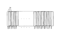
- FIG. 8 is a diagram for explaining selection control of a plurality of switches of the select switches 211A and 212A in the electromagnetic induction mode in the position detection apparatus 1A of the second example of the second embodiment.
- the select switch 211A and the select switch 212A of the selection circuit 21A sequentially select the same three adjacent loop electrodes X, but the loop electrodes X1, X2, and X3 are connected first.
- the three switches are turned on, and the loop electrodes X1, X2, and X3 are connected to the common terminals XA ′ and XB ′.
- the three switches connected to the loop electrodes X2, X3, and X4 are turned on, and the loop electrodes X2, X3, and X4 are connected to the common terminals XA ′ and XB ′.
- loop electrodes X3, X4 and X5, X4, X5 and X6, X5, X6 and X7 are shifted one by one while shifting the three loop electrodes X to the common terminals XA ′ and XB. Connect to ⁇ .
- the three loop electrodes X (coils) are connected in parallel and supplied to the X-side differential input amplifier 24X. It becomes a state.
- the X-side differential input amplifier 24X provides an output ⁇ (i1 + i2 + i3) corresponding to the sum of the currents induced in these three loop electrodes Xn, Xn + 1 and Xn + 2.
- the select switch 211A and the select switch 212A sequentially select the three adjacent loop electrodes X in the order shown in FIG. As shown in FIG. 10, this is equivalent to a well-known detection method in the electromagnetic induction system in which loop coils 15 that are arranged overlapping each other are selected in order.
- a loop coil having a width three times the arrangement pitch of the loop electrodes X can be formed by selecting three adjacent loop electrodes simultaneously.
- the selection circuit 22A for the Y loop electrode group 13 for obtaining the Y coordinate can be similarly configured, and three coils are connected in parallel to be supplied to the Y side differential input amplifier 24Y. .
- the selection circuit 21A and the selection circuit 22A have a plurality of loop electrodes X and a plurality of loop electrodes as shown in FIGS.
- the selection circuit is configured so that the loop electrodes (coils) are connected in series when a plurality of adjacent loop electrodes X and a plurality of loop electrodes Y are selected. You can also.
- the third embodiment is an example in that case.
- FIG. 11 is a diagram for explaining a configuration example of the position detection apparatus 1B according to the third embodiment. In the following description, the operation in the electromagnetic induction mode of the position detection device 1B of the third embodiment will be mainly described.
- a selection circuit 21B and a selection circuit 22B instead of the selection circuit 21 and the selection circuit 22 in the position detection device 1 of the first embodiment, a selection circuit 21B and a selection circuit 22B. And a processing control circuit 26B is provided instead of the processing control circuit 26.
- the other configuration is the same as that of the position detection device 1 of the first embodiment.
- the same parts as those of the position detection device 1 of the first embodiment described above are denoted by the same reference numerals, and the description thereof is omitted.
- the pen signal receiving circuit 24 and the touch detection control circuit 25 are not shown.
- the selection circuit 21B includes a plurality of multiplexers 211B and 212B having the same configuration as the multiplexers 211 and 212 of the first embodiment, and the number of loop electrodes X (X1 to X40) in this example. It is composed of 39 three-terminal switches SX1 to SX39, which is one less than a minute.
- the three-terminal switch has three terminals, a first terminal, a second terminal, and a third terminal, and is set to connect any two terminals among these three terminals by a setting control signal. It is a switch that can do.
- each of the winding end ends X1b to X39b of the loop electrode X (X1 to X39) is connected to the first terminal of each of the three-terminal switches SX1 to SX39, and the winding start end X2a of the loop electrode X (X2 to X40).
- To X40a are connected to the second terminals of the three-terminal switches SX1 to SX39.
- the third terminals of the three-terminal switches SX1 to SX39 are connected to the multiplexers 211B and 212B.
- the winding start end X1a of the loop electrode X1 is directly connected to the multiplexer 212B
- the winding end X40b of the loop electrode X40 is directly connected to the multiplexer 211B.
- the processing control circuit 26B sends a setting control signal CTx for controlling the setting to each of the three-terminal switches SX1 to SX39, A selection control signal SExA and a selection control signal SExB are sent to the multiplexer 211B and the multiplexer 212B, respectively.
- the three-terminal switch SX1 in which the winding end X1b of the loop electrode X1 is connected to the first terminal is connected to the first terminal SX1.
- the three-terminal switch SX2 is controlled so that the first terminal is connected to the second terminal, and the winding end X2b of the adjacent loop electrode X2 is connected to the first terminal.
- Settings are controlled so that the terminal and the third terminal are connected.
- the multiplexer 211B selects the three-terminal switch SX2, and the multiplexer 212B is controlled to select the winding start end X1a of the loop electrode X1.
- the 3-terminal switch SX1 is set and controlled so that the first terminal and the third terminal are connected, and the adjacent 3-terminal switch SX2 is connected to the first terminal and the second terminal. Settings are controlled so that they are connected, and further, the adjacent three-terminal switch SX3 is controlled so that the first terminal and the third terminal are connected. Then, the multiplexer 211B selects the three-terminal switch SX3 in which the first terminal and the third terminal are connected, and the multiplexer 212B similarly connects the first terminal and the third terminal. Selection control is performed so as to select the three-terminal switch SX1.
- the set of three adjacent three-terminal switches SXn to SXn + 2 is sequentially shifted and controlled by one three-terminal switch.
- the three-terminal switches SXn and SXn + 2 at both ends have the first terminal connected to the third terminal, and the central three-terminal switch SXn + 1 has the first The terminal is controlled to be connected to the second terminal.
- the multiplexer 211B and the multiplexer 212B are controlled so as to select the three-terminal switch SXn + 2 and the three-terminal switch SXn at both ends.
- the two loop electrodes X (coils) are connected in series and supplied to the X-side differential input amplifier 24X.
- an output corresponding to the added value of the currents induced in the two loop electrodes X is obtained in the X-side differential input amplifier 24X.
- the winding start ends of the loop electrodes X at both ends are connected to the multiplexers 211B and 212B, and the loop electrodes X between the both ends are adjacent to each other, but the winding end ends and winding start ends are Each of the three-terminal switches to which the plurality of loop electrodes X are connected is controlled so as to be connected.
- the selection circuit 22B for the Y loop electrode group 13 is also configured in the same manner, and similarly controlled to connect a plurality of loop electrodes Y in series. can do. That is, the selection circuit 22B includes a plurality of multiplexers 221B and 222B having the same configuration as the multiplexers 221 and 222 of the first embodiment, and a number that is one less than the number of loop electrodes Y (Y1 to Y30) in this example. This is composed of 29 three-terminal switches SY1 to SY29.
- the multiplexers 221B and 222B and the three-terminal switches SY1 to SY29 of the selection circuit 22B are controlled by the selection control signals SEyA and SEyB and the setting control signal CTy from the processing control circuit 26B, so that the X loop electrode group As in the case of 12, it is possible to select a plurality of adjacent loop electrodes Y by sequentially connecting them in series.
- the loop circuit X and the loop electrode Y are selected one by one by the selection circuit 21B and the selection circuit 22B, as in the second embodiment. To do.
- the position detection sensor 10 includes the loop electrode X and the loop electrode using a conductive material that can be made substantially transparent, such as a metal mesh electrode in which a transparent substrate 11 is combined with fine wires such as ITO, silver, or copper. Y was formed.
- the electrode lines constituting the position detection sensor 10 are formed as a pattern having a predetermined width of about 1 millimeter, for example.
- the inner part of the width of the loop electrode X and the width of the loop electrode Y becomes electrically hollow. The capacity decreases at the center of the loop electrode X and the loop electrode Y, and it becomes difficult to accurately obtain the position indicated by the finger.
- FIGS. 13A and 13B show examples of protrusions that protrude from the line pattern of the electrodes constituting the loop electrode X and the loop electrode Y to the inside of the width of the loop electrode X and the inside of the width of the loop electrode Y. is there.
- the loop electrode X and the loop electrode Y are arranged so as to intersect at right angles.
- a rectangular cavity region 16 is formed by the width of Y.
- the electrode lines of the loop electrode X are opposed to each other at the position toward the center of the rectangular cavity region 16 and project in a direction perpendicular to the electrode line pattern.
- a plurality of protrusions 17a and 17b are formed.
- two protruding portions 18a and 18b that protrude in a direction orthogonal to the electrode line pattern at the center position of the rectangular cavity region 16 are formed. Is done.
- protrusions 17c and 17d that protrude in a direction orthogonal to the electrode line pattern of the loop electrode X are formed, but in this example, the rectangular cavity region 16 is formed.
- These projecting portions 17c and 17d are formed so as to be shifted from the center of each other so as not to face each other.
- protrusions 18c and 18d projecting in a direction intersecting perpendicularly to the electrode line pattern of the loop electrode Y are formed, but in this example, toward a position shifted from the center of the rectangular cavity region 16.
- the protrusions 18c and 18d are formed in a state where they are not opposed to each other.
- the cavity region 16 has a protrusion. Since the portions 17a and 17b and the protrusions 18a and 18b or the protrusions 17c and 17d and the protrusions 18c and 18d are present, the finger is substantially in contact with the loop electrode X and the loop electrode Y. It becomes easier to detect.
- the projections 17a and 17b and the projections 18a and 18b or the projections 17c and 17d and the projections 18c and 18d are provided inside the loop electrodes X and Y, the magnetic field radiated from the electronic pen is In the pen signal reception operation, the projections 17a and 17b and the projections 18a and 18b or the projections 17c and 17d and the projections 18c and 18d are When receiving the magnetic field signal from the electronic pen, there is almost no influence.
- each of the loop electrode X and the loop electrode Y is short-circuited by connecting the winding start end and the winding end end.
- One of the end ends may be an open end (release end), and the other end may be an end for connecting to the touch detection control circuit 25.
- the position detection sensor 10 has a configuration of a transparent sensor in which the loop electrode X and the loop electrode Y are formed by the metal mesh electrode in which the transparent substrate 11 is combined with fine wires such as ITO, silver, and copper.
- the configuration of the opaque sensor may be used for applications other than the application on the display screen of the display device.
- the X-side input and Y-side input amplifier circuits of the pen signal receiving circuit 24 are configured as differential amplifiers, but one end of each of the loop electrode X and the loop electrode Y is connected to a fixed potential. The other end may be supplied to a single-input amplifier.
- the position detection devices 1, 1A, 1B are configured to execute the electromagnetic induction mode and the electrostatic coupling mode in a time-sharing manner based on the mode switching signal MD from the processing control circuits 26, 26A, 26B. Switched to.
- switching between the electromagnetic induction mode and the electrostatic coupling mode may be performed manually by the user.
- the position detection device is provided with a changeover switch and a pushbutton switch that can be changed by the user.
- the processing control circuit can change the electromagnetic induction mode according to the changeover state of the changeover switch or the pushbutton switch. Switch between electrostatic coupling modes.
- the position detection device when the position detection device is in a state of receiving a signal from the electronic pen through the position detection sensor, the position detection device is switched to the electromagnetic induction mode, and in a state of not receiving the signal from the electronic pen through the position detection sensor, You may switch so that it may be set to the electric coupling mode.
- a Bluetooth (registered trademark) standard short-range wireless communication circuit is provided in both the electronic pen and the position detection device, and the short-range wireless communication circuit of the position detection device receives a signal from the electronic pen.
- the position detection device When the position detection device is switched to the electromagnetic induction mode and no signal is received from the electronic pen, the position detection device may be switched to the electrostatic coupling mode.
- the second indicator as a target to be detected in the electrostatic coupling mode is a human finger, but may be a passive electrostatic electronic pen. Further, an active electrostatic coupling type electronic pen may be used. In the case of an active electrostatic coupling type electronic pen, instead of the touch detection control circuit 25, a signal from the active electrostatic coupling type electronic pen is received for each of the loop electrode X and the loop electrode Y, A circuit for detecting the level is provided.
- the position indicated by the electronic pen 2 is detected by receiving a signal from the electronic pen 2 including the oscillation circuit.
- the present invention is not limited to this, and an electronic pen having a resonance circuit composed of a coil and a capacitor is used.
- an AC signal is transmitted from the position detection device to the electronic pen by electromagnetic induction coupling. It is also possible to adopt a configuration in which the position indicated by the electronic pen is detected by receiving a signal fed back via the resonance circuit of the electronic pen.
- the X loop electrode group 12 and the Y loop electrode group 13 may be used, or a loop coil may be separately provided for transmission.
Landscapes
- Engineering & Computer Science (AREA)
- General Engineering & Computer Science (AREA)
- Theoretical Computer Science (AREA)
- Physics & Mathematics (AREA)
- Human Computer Interaction (AREA)
- General Physics & Mathematics (AREA)
- Electromagnetism (AREA)
- Computer Networks & Wireless Communication (AREA)
- Measurement Of Length, Angles, Or The Like Using Electric Or Magnetic Means (AREA)
- Position Input By Displaying (AREA)
- External Artificial Organs (AREA)
- Near-Field Transmission Systems (AREA)
Priority Applications (23)
| Application Number | Priority Date | Filing Date | Title |
|---|---|---|---|
| KR1020207022421A KR102671281B1 (ko) | 2018-02-13 | 2018-11-15 | 위치 검출 장치, 그리고 전자 유도 결합 및 정전 결합에 기초하는 위치 검출 방법 |
| KR1020257021220A KR20250100791A (ko) | 2018-02-13 | 2018-11-15 | 위치 검출 장치, 그리고 전자 유도 결합 및 정전 결합에 기초하는 위치 검출 방법 |
| CN202411393335.4A CN119376568A (zh) | 2018-02-13 | 2018-11-15 | 位置检测装置以及控制装置 |
| CN202411391753.XA CN119376566A (zh) | 2018-02-13 | 2018-11-15 | 位置检测装置以及控制装置 |
| KR1020247017837A KR102826880B1 (ko) | 2018-02-13 | 2018-11-15 | 위치 검출 장치, 그리고 전자 유도 결합 및 정전 결합에 기초하는 위치 검출 방법 |
| EP25208208.6A EP4692999A3 (en) | 2018-02-13 | 2018-11-15 | Position detection device, and position detection method based on electromagnetic inductive coupling and capacitive coupling |
| JP2020500277A JP7079838B2 (ja) | 2018-02-13 | 2018-11-15 | 位置検出装置、ならびに電磁誘導結合及び静電結合に基づく位置検出方法 |
| CN202411393010.6A CN119376567A (zh) | 2018-02-13 | 2018-11-15 | 位置检测装置以及控制装置 |
| CN202411393719.6A CN119376569A (zh) | 2018-02-13 | 2018-11-15 | 位置检测装置 |
| CN202411390688.9A CN119376564A (zh) | 2018-02-13 | 2018-11-15 | 位置检测装置以及控制装置 |
| EP18906401.7A EP3739434B1 (en) | 2018-02-13 | 2018-11-15 | Position detection device and position detection method based on electromagnetic induction coupling and electrostatic coupling |
| CN202411391207.6A CN119376565A (zh) | 2018-02-13 | 2018-11-15 | 位置检测装置以及控制装置 |
| CN201880072381.0A CN111316212B (zh) | 2018-02-13 | 2018-11-15 | 位置检测装置以及基于电磁感应耦合及静电耦合的位置检测方法 |
| US16/986,204 US11249610B2 (en) | 2018-02-13 | 2020-08-05 | Position detection device, and position detection method based on electromagnetic inductive coupling and capacitive coupling |
| US17/559,954 US11644936B2 (en) | 2018-02-13 | 2021-12-22 | Position detection device, and position detection method based on electromagnetic inductive coupling and capacitive coupling |
| JP2022083482A JP7421596B2 (ja) | 2018-02-13 | 2022-05-23 | 位置検出装置 |
| US18/194,453 US12008206B2 (en) | 2018-02-13 | 2023-03-31 | Position detection device, and position detection method based on electromagnetic inductive coupling and capacitive coupling |
| JP2024003028A JP7714061B2 (ja) | 2018-02-13 | 2024-01-12 | 位置検出装置及び位置検出方法 |
| US18/652,659 US12271566B2 (en) | 2018-02-13 | 2024-05-01 | Position detection device, and position detection method based on electromagnetic inductive coupling and capacitive coupling |
| US19/029,926 US20250165112A1 (en) | 2018-02-13 | 2025-01-17 | Position detection device, and position detection method based on electromagnetic inductive coupling and capacitive coupling |
| US19/030,163 US20250165113A1 (en) | 2018-02-13 | 2025-01-17 | Position detection device, and position detection method based on electromagnetic inductive coupling and capacitive coupling |
| US19/029,475 US20250165111A1 (en) | 2018-02-13 | 2025-01-17 | Position detection device, and position detection method based on electromagnetic inductive coupling and capacitive coupling |
| JP2025118671A JP2025133974A (ja) | 2018-02-13 | 2025-07-15 | 位置検出装置 |
Applications Claiming Priority (2)
| Application Number | Priority Date | Filing Date | Title |
|---|---|---|---|
| JP2018022683 | 2018-02-13 | ||
| JP2018-022683 | 2018-02-13 |
Related Child Applications (1)
| Application Number | Title | Priority Date | Filing Date |
|---|---|---|---|
| US16/986,204 Continuation US11249610B2 (en) | 2018-02-13 | 2020-08-05 | Position detection device, and position detection method based on electromagnetic inductive coupling and capacitive coupling |
Publications (1)
| Publication Number | Publication Date |
|---|---|
| WO2019159456A1 true WO2019159456A1 (ja) | 2019-08-22 |
Family
ID=67618519
Family Applications (1)
| Application Number | Title | Priority Date | Filing Date |
|---|---|---|---|
| PCT/JP2018/042223 Ceased WO2019159456A1 (ja) | 2018-02-13 | 2018-11-15 | 位置検出装置、ならびに電磁誘導結合及び静電結合に基づく位置検出方法 |
Country Status (7)
| Country | Link |
|---|---|
| US (7) | US11249610B2 (https=) |
| EP (2) | EP4692999A3 (https=) |
| JP (4) | JP7079838B2 (https=) |
| KR (3) | KR102671281B1 (https=) |
| CN (7) | CN119376566A (https=) |
| TW (1) | TWI798296B (https=) |
| WO (1) | WO2019159456A1 (https=) |
Cited By (3)
| Publication number | Priority date | Publication date | Assignee | Title |
|---|---|---|---|---|
| WO2023238641A1 (ja) * | 2022-06-10 | 2023-12-14 | 株式会社ワコム | 位置検出装置、電磁誘導ペン、及び、位置検出システム |
| JP2024511467A (ja) * | 2021-03-26 | 2024-03-13 | 株式会社 ハイディープ | タッチ入力装置 |
| WO2024116795A1 (ja) * | 2022-11-28 | 2024-06-06 | 株式会社ワコム | 位置検出装置及び電子機器 |
Families Citing this family (15)
| Publication number | Priority date | Publication date | Assignee | Title |
|---|---|---|---|---|
| TWI730591B (zh) * | 2020-01-15 | 2021-06-11 | 興城科技股份有限公司 | 玻璃基板檢測設備及其方法 |
| WO2022097340A1 (ja) | 2020-11-06 | 2022-05-12 | 株式会社ワコム | センサ |
| TWI818421B (zh) * | 2021-01-29 | 2023-10-11 | 南韓商希迪普公司 | 觸控裝置、其之驅動方法及觸控系統 |
| JP7664720B2 (ja) * | 2021-03-15 | 2025-04-18 | 株式会社ワコム | 位置検出センサおよび位置検出装置 |
| KR102773716B1 (ko) * | 2021-04-13 | 2025-02-27 | 주식회사 하이딥 | 터치 입력 장치 |
| US11923842B1 (en) | 2023-01-04 | 2024-03-05 | Dell Products L.P. | System and method for obtaining user input with keyboard integrated magnetic sensing |
| US12136528B2 (en) | 2023-01-04 | 2024-11-05 | Dell Products L.P. | System and method for obtaining user input with passive keyboard |
| US11809646B1 (en) | 2023-03-09 | 2023-11-07 | Dell Products L.P. | System and method for obtaining user input in portable systems |
| US11874687B1 (en) | 2023-03-09 | 2024-01-16 | Dell Products L.P. | System and method for obtaining user input using passive human interface device |
| US11886700B1 (en) * | 2023-03-09 | 2024-01-30 | Dell Products L.P. | System and method for magnetic sensing multiconfiguration data processing systems |
| US11868551B1 (en) | 2023-03-09 | 2024-01-09 | Dell Products L.P. | System and method for customized user input |
| DE102023202826A1 (de) * | 2023-03-28 | 2024-10-02 | Infineon Technologies Ag | Induktives positionsmesssystem zum bestimmen einer bewegung entlang einer gekrümmten bahn |
| US12591321B2 (en) | 2024-07-30 | 2026-03-31 | Dell Products L.P. | Dial based human interface device |
| US12596443B2 (en) | 2024-07-30 | 2026-04-07 | Dell Products L.P. | System and method for obtaining user input with magnetic sensing using a track ball |
| US12493369B1 (en) | 2024-07-30 | 2025-12-09 | Dell Products L.P. | Human interface device sensing |
Citations (4)
| Publication number | Priority date | Publication date | Assignee | Title |
|---|---|---|---|---|
| JPS572511B2 (https=) | 1973-05-08 | 1982-01-16 | ||
| JPS5819565B2 (ja) | 1974-12-20 | 1983-04-19 | 株式会社ブリヂストン | ユソウヨウベルトホゴソウチ |
| JP2014164770A (ja) * | 2013-02-27 | 2014-09-08 | Samsung Display Co Ltd | 表示装置及び表示装置の駆動方法 |
| JP2015041318A (ja) * | 2013-08-23 | 2015-03-02 | 株式会社シロク | 座標検出装置 |
Family Cites Families (27)
| Publication number | Priority date | Publication date | Assignee | Title |
|---|---|---|---|---|
| JPS572511U (https=) | 1980-06-05 | 1982-01-07 | ||
| JPS5819565U (ja) | 1981-07-28 | 1983-02-07 | 株式会社横河電機製作所 | ドキユメント入力装置 |
| JPS5924388A (ja) * | 1982-07-31 | 1984-02-08 | Osukon Denshi Kk | 座標読取り装置 |
| JP2971488B2 (ja) * | 1989-11-01 | 1999-11-08 | 株式会社ワコム | 位置検出装置 |
| JPH07129305A (ja) * | 1993-10-29 | 1995-05-19 | Graphtec Corp | コードレスデジタイザ |
| US5434372A (en) * | 1993-08-19 | 1995-07-18 | Acer Peripherals, Inc. | Position detecting apparatus with coils of opposite loop direction |
| JP3411118B2 (ja) * | 1994-03-31 | 2003-05-26 | グラフテック株式会社 | デジタイザおよびデジタイザの位置決定方法 |
| EP2028585B1 (en) * | 2007-08-21 | 2010-07-14 | Wacom Co., Ltd. | Information processing apparatus, operation input method and computer program product |
| JP2009193534A (ja) | 2008-02-18 | 2009-08-27 | Sega Corp | 指示位置検出装置及び指示位置検出方法 |
| US8482545B2 (en) * | 2008-10-02 | 2013-07-09 | Wacom Co., Ltd. | Combination touch and transducer input system and method |
| US8466692B2 (en) | 2011-04-28 | 2013-06-18 | Waltop International Corporation | Electromagnetic sensor system and antenna loop layout method thereof |
| US9160331B2 (en) * | 2011-10-28 | 2015-10-13 | Atmel Corporation | Capacitive and inductive sensing |
| JP5848589B2 (ja) * | 2011-12-02 | 2016-01-27 | 株式会社ワコム | 位置検出装置および位置検出方法 |
| KR101209514B1 (ko) * | 2012-07-25 | 2012-12-07 | (주)이미지스테크놀로지 | 자기장의 변화와 정전용량의 변화를 감지하는 터치 입력 장치 |
| KR102049261B1 (ko) * | 2012-09-14 | 2019-11-29 | 삼성디스플레이 주식회사 | 표시장치 |
| JP5984259B2 (ja) * | 2012-09-20 | 2016-09-06 | 株式会社ワコム | 位置検出装置 |
| KR101516059B1 (ko) * | 2012-12-26 | 2015-05-04 | 삼성전기주식회사 | 터치 스크린 및 이의 구동 방법 |
| KR101487463B1 (ko) * | 2013-07-03 | 2015-01-28 | 주식회사 더한 | 전자기 유도 방식의 위치감지와 정전용량 방식의 위치감지를 수행할 수 있는 타블렛 |
| KR101501422B1 (ko) | 2013-12-03 | 2015-03-10 | 뉴콤 테크노 가부시키가이샤 | 지정 위치 검출 장치 |
| WO2015137053A1 (ja) * | 2014-03-10 | 2015-09-17 | 株式会社ワコム | 位置検出装置 |
| TW201614448A (en) * | 2014-06-25 | 2016-04-16 | Np Holdings Co Ltd | Coordinate input device with advanced touch sensing |
| EP2998842A4 (en) | 2014-07-25 | 2017-05-03 | Newcom Techno Inc. | Position detection unit |
| KR102344098B1 (ko) * | 2014-10-06 | 2021-12-28 | 가부시키가이샤 와코무 | 위치 지시기 |
| CN104484071B (zh) * | 2014-12-25 | 2018-01-02 | 上海天马微电子有限公司 | 一种触控面板和触控装置及其驱动方法 |
| JP6789210B2 (ja) * | 2015-03-31 | 2020-11-25 | 株式会社ワコム | 電子ペン及び電子ペン本体部 |
| JP6605292B2 (ja) * | 2015-10-16 | 2019-11-13 | 株式会社ジャパンディスプレイ | 表示装置 |
| JP6532105B2 (ja) * | 2015-12-17 | 2019-06-19 | 株式会社ワコム | タッチパネル、信号処理装置及びグランドカップリング方法 |
-
2018
- 2018-11-15 CN CN202411391753.XA patent/CN119376566A/zh active Pending
- 2018-11-15 CN CN202411390688.9A patent/CN119376564A/zh active Pending
- 2018-11-15 KR KR1020207022421A patent/KR102671281B1/ko active Active
- 2018-11-15 CN CN202411393719.6A patent/CN119376569A/zh active Pending
- 2018-11-15 JP JP2020500277A patent/JP7079838B2/ja active Active
- 2018-11-15 KR KR1020247017837A patent/KR102826880B1/ko active Active
- 2018-11-15 CN CN202411391207.6A patent/CN119376565A/zh active Pending
- 2018-11-15 WO PCT/JP2018/042223 patent/WO2019159456A1/ja not_active Ceased
- 2018-11-15 KR KR1020257021220A patent/KR20250100791A/ko active Pending
- 2018-11-15 CN CN201880072381.0A patent/CN111316212B/zh active Active
- 2018-11-15 EP EP25208208.6A patent/EP4692999A3/en active Pending
- 2018-11-15 EP EP18906401.7A patent/EP3739434B1/en active Active
- 2018-11-15 CN CN202411393335.4A patent/CN119376568A/zh active Pending
- 2018-11-15 CN CN202411393010.6A patent/CN119376567A/zh active Pending
- 2018-11-26 TW TW107142072A patent/TWI798296B/zh active
-
2020
- 2020-08-05 US US16/986,204 patent/US11249610B2/en active Active
-
2021
- 2021-12-22 US US17/559,954 patent/US11644936B2/en active Active
-
2022
- 2022-05-23 JP JP2022083482A patent/JP7421596B2/ja active Active
-
2023
- 2023-03-31 US US18/194,453 patent/US12008206B2/en active Active
-
2024
- 2024-01-12 JP JP2024003028A patent/JP7714061B2/ja active Active
- 2024-05-01 US US18/652,659 patent/US12271566B2/en active Active
-
2025
- 2025-01-17 US US19/030,163 patent/US20250165113A1/en active Pending
- 2025-01-17 US US19/029,926 patent/US20250165112A1/en active Pending
- 2025-01-17 US US19/029,475 patent/US20250165111A1/en active Pending
- 2025-07-15 JP JP2025118671A patent/JP2025133974A/ja active Pending
Patent Citations (4)
| Publication number | Priority date | Publication date | Assignee | Title |
|---|---|---|---|---|
| JPS572511B2 (https=) | 1973-05-08 | 1982-01-16 | ||
| JPS5819565B2 (ja) | 1974-12-20 | 1983-04-19 | 株式会社ブリヂストン | ユソウヨウベルトホゴソウチ |
| JP2014164770A (ja) * | 2013-02-27 | 2014-09-08 | Samsung Display Co Ltd | 表示装置及び表示装置の駆動方法 |
| JP2015041318A (ja) * | 2013-08-23 | 2015-03-02 | 株式会社シロク | 座標検出装置 |
Cited By (4)
| Publication number | Priority date | Publication date | Assignee | Title |
|---|---|---|---|---|
| JP2024511467A (ja) * | 2021-03-26 | 2024-03-13 | 株式会社 ハイディープ | タッチ入力装置 |
| JP7646246B2 (ja) | 2021-03-26 | 2025-03-21 | 株式会社 ハイディープ | タッチ入力装置 |
| WO2023238641A1 (ja) * | 2022-06-10 | 2023-12-14 | 株式会社ワコム | 位置検出装置、電磁誘導ペン、及び、位置検出システム |
| WO2024116795A1 (ja) * | 2022-11-28 | 2024-06-06 | 株式会社ワコム | 位置検出装置及び電子機器 |
Also Published As
Similar Documents
| Publication | Publication Date | Title |
|---|---|---|
| JP7421596B2 (ja) | 位置検出装置 | |
| TWI705360B (zh) | 觸控面板、訊號處理裝置及耦合方法 | |
| JP4872113B2 (ja) | 位置検出装置 | |
| KR102151545B1 (ko) | 위치 검출 장치 | |
| US20160041677A1 (en) | Position detecting unit | |
| CN109426369B (zh) | 位置检测传感器以及位置检测装置 | |
| JP2015049890A (ja) | 位置感知方法、位置感知装置、アンテナ装置、及びディスプレイ装置 | |
| JP2026069734A (ja) | 端末装置および位置検出センサ | |
| KR20140046275A (ko) | 펜의 위치를 측정하는 위치 측정 장치 및 그 제어 방법 |
Legal Events
| Date | Code | Title | Description |
|---|---|---|---|
| 121 | Ep: the epo has been informed by wipo that ep was designated in this application |
Ref document number: 18906401 Country of ref document: EP Kind code of ref document: A1 |
|
| ENP | Entry into the national phase |
Ref document number: 2020500277 Country of ref document: JP Kind code of ref document: A |
|
| ENP | Entry into the national phase |
Ref document number: 20207022421 Country of ref document: KR Kind code of ref document: A |
|
| NENP | Non-entry into the national phase |
Ref country code: DE |
|
| ENP | Entry into the national phase |
Ref document number: 2018906401 Country of ref document: EP Effective date: 20200814 |
|
| WWD | Wipo information: divisional of initial pct application |
Ref document number: 1020257021220 Country of ref document: KR |
|
| WWP | Wipo information: published in national office |
Ref document number: 1020257021220 Country of ref document: KR |
|
| WWG | Wipo information: grant in national office |
Ref document number: 2018906401 Country of ref document: EP |