WO2019150844A1 - 光学素子の成形方法 - Google Patents
光学素子の成形方法 Download PDFInfo
- Publication number
- WO2019150844A1 WO2019150844A1 PCT/JP2018/047368 JP2018047368W WO2019150844A1 WO 2019150844 A1 WO2019150844 A1 WO 2019150844A1 JP 2018047368 W JP2018047368 W JP 2018047368W WO 2019150844 A1 WO2019150844 A1 WO 2019150844A1
- Authority
- WO
- WIPO (PCT)
- Prior art keywords
- molding
- mold
- molding material
- die
- viscosity
- Prior art date
- Legal status (The legal status is an assumption and is not a legal conclusion. Google has not performed a legal analysis and makes no representation as to the accuracy of the status listed.)
- Ceased
Links
Images

Classifications
-
- C—CHEMISTRY; METALLURGY
- C03—GLASS; MINERAL OR SLAG WOOL
- C03B—MANUFACTURE, SHAPING, OR SUPPLEMENTARY PROCESSES
- C03B11/00—Pressing molten glass or performed glass reheated to equivalent low viscosity without blowing
-
- C—CHEMISTRY; METALLURGY
- C03—GLASS; MINERAL OR SLAG WOOL
- C03B—MANUFACTURE, SHAPING, OR SUPPLEMENTARY PROCESSES
- C03B11/00—Pressing molten glass or performed glass reheated to equivalent low viscosity without blowing
- C03B11/12—Cooling, heating, or insulating the plunger, the mould, or the glass-pressing machine; cooling or heating of the glass in the mould
-
- G—PHYSICS
- G02—OPTICS
- G02B—OPTICAL ELEMENTS, SYSTEMS OR APPARATUS
- G02B3/00—Simple or compound lenses
Definitions
- the present invention relates to a method for molding an optical element.
- Patent Document 1 when the molding material is pressed and deformed, by monitoring the approach speed of the upper mold with respect to the lower mold, it is detected that the molding material is filled in the cavity based on a decrease in the approach speed, A method of forming an optical element is disclosed in which the pressure deformation is terminated after detecting the filling and then cooled and cured.
- the molding die is cooled to cure the molding material. Therefore, when the molding material is pressed and deformed, the molding material M softened in the gap between the upper die 11 and the side die 13 and the gap between the lower die 12 and the side die 13, for example, as shown in part A of FIG. 4. There was a case of getting in. As a result, the molding material M that has entered the gap becomes a burr after cooling and hardening, and the burr is caught at the time of taking out and there is a possibility that the optical element is cracked.
- the molding method disclosed in Patent Document 1 since the pressure on the outer peripheral side of the molding material M is pressed in a state lower than the temperature of the center portion, the contact position between the molding material M and the inner surface of the side mold 13 is local. Therefore, there was a possibility that the molding material M might be seized on the inner surface of the side mold 13. Further, in the molding method disclosed in Patent Document 1, although the molding material M is filled in the cavity, the contact time of the molding material M with the inner surface of the side mold 13 and the outer peripheral portion of the molding surface in the vicinity thereof is the upper mold 11. The contact time of the molding material M with respect to the central portion of the molding surface 11a and the central portion of the molding surface 12a of the lower mold 12 is shorter. For this reason, there is a possibility that the surface accuracy of the outer peripheral portion of the optical element after molding and the outer peripheral portion of the molding surface cannot be ensured.
- the present invention has been made in view of the above, and a method for molding an optical element capable of suppressing cracking and seizure of the optical element and ensuring the surface accuracy of the outer peripheral portion of the optical element and the outer peripheral portion of the molding surface.
- the purpose is to provide.
- an optical element molding method presses a molding material arranged in a molding die composed of an upper die, a lower die, and a side die.
- the molding material does not enter the gap between the upper mold and the side mold and the gap between the lower mold and the side mold.
- the optical element molding method according to the present invention is the above invention, wherein the molding die is heated in the second pressing step so that the surface temperature of the molding material is higher than the first viscosity.
- the second temperature is set to a low second viscosity, and a second pressing force smaller than the first pressing force is applied to the molding material.
- the optical element molding method according to the present invention is the above-described invention, wherein the upper mold and the lower mold are disposed between the heating step and the first pressing step or during the first pressing step.
- the activity of the material surface is lowered by lowering the temperature of one or more of the side molds, and the viscosity of the surface of the molding material is made higher than the first viscosity.
- the activity of the material surface is lowered to suppress seizure with the molding die, and the gap between the upper die and the side die and the lower die Since the molding material can be prevented from entering the gap between the side mold and the side mold, it is possible to suppress the fragility of the optical element caused by burrs caused by the molding material entering.
- molding and a molding surface outer peripheral part is securable.
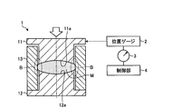
- FIG. 1 is a cross-sectional view schematically showing a configuration of a molding die used in the method for molding an optical element according to the embodiment of the present invention.
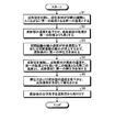
- FIG. 2 is a flowchart showing the procedure of the optical element molding method according to the embodiment of the present invention.
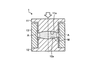
- FIG. 3 is a cross-sectional view schematically showing a molding material after pressing in the optical element molding method according to the embodiment of the present invention.
- FIG. 4 is a cross-sectional view schematically showing a molding material after pressing in the conventional optical element molding method.
- the optical element molding method according to the present embodiment presses a molding material arranged in a molding die composed of an upper die, a lower die, and a side die, thereby providing an optical surface by the upper die and the lower die, This is a method of molding an optical element having a side surface transferred by a side mold.
- a molding die 1 As shown in FIG. 1, a molding die 1, a position gauge 2, a timer 3, and a control unit 4 are used.
- the molding die 1 includes an upper die 11 having a molding surface 11a formed at one end, a lower die 12 having a molding surface 12a formed at one end, and a side die (sleeve) 13.
- a cavity Ca that is a space surrounded by the upper mold 11, the lower mold 12, and the side mold 13 is formed inside the mold 1, and the molding material M is disposed in the cavity Ca.
- the molding surface 11a of the upper mold 11 and the molding surface 12a of the lower mold 12 are arranged to face each other with the molding material M in between.
- the side mold 13 is for sliding and guiding the upper mold 11 and the lower mold 12.
- the side mold 13 is formed in a cylindrical shape as a whole, and holds the upper mold 11 and the lower mold 12 so as to be freely inserted and removed. Note that gaps necessary for sliding during mold operation are formed between the upper mold 11 and the side mold 13 and between the lower mold 12 and the side mold 13.
- each mold constituting the mold 1 is configured to be heated by a heater unit (not shown), and the molding material M disposed inside the mold 1 can be indirectly heated. As will be described later, the molding material M heated and softened by the molding die 1 is deformed by the approaching action of the upper die 11 and the lower die 12, and is shaped into the shape of the optical element.
- the position gauge 2, the timer 3 and the control unit 4 are for monitoring the speed at which the distance between the upper mold 11 and the lower mold 12 is reduced when the molding material M is pressed.
- the position gauge 2 measures the relative distance of the upper mold 11 relative to the lower mold 12 when the upper mold 11 is approaching the lower mold 12, and outputs the information to the control unit 4.
- the timer 3 measures the time when the upper mold 11 is approaching the lower mold 12 and outputs the information to the control unit 4.
- control unit 4 calculates the speed at which the distance between the molds is reduced based on these pieces of information, and whether or not the reduction speed of the distance between the molds of the upper mold 11 and the lower mold 12 is equal to or lower than a predetermined speed, or Detects whether the reduction of the distance between the molds has stopped.
- a method for molding an optical element according to the present embodiment will be described with reference to FIGS.
- a heating process, a first pressing process, a second pressing process, a cooling process, and a mold releasing process are performed.
- a surface temperature (viscosity) adjusting step is performed between the heating step and the first pressing step, or during the first pressing step, as necessary.
- the molding material M does not enter the gap between the molding dies 1 when the molding die 1 is heated to apply the first pressing force set in advance to the temperature of the molding material M. It is set as the 1st temperature used as the 1st viscosity (refer Step S1 of Drawing 2).
- the above-mentioned “gap between the molds of the mold 1” specifically means a gap between the upper mold 11 and the side mold 13 and a gap between the lower mold 12 and the side mold 13.
- the molding die 1 is heated by a heater unit (not shown), thereby heating the molding material M disposed in the cavity Ca of the molding die 1 to the first temperature, Soften to one viscosity.
- This first temperature is in the range from the TG point (glass transition point) to the SP point (softening point) of the molding material M, and with respect to the first pressing force in the first pressing step described later, the mold 1 Is a temperature at which the softened molding material M cannot enter the gap between the molds (first viscosity).
- the heating process by changing the set temperature of the heater unit provided in the upper mold 11 and the lower mold 12, the vertical difference in formability due to the shape factor and the shape of the mold can be adjusted.
- the first temperature is determined by experimental determination in advance in consideration of the heating temperature of the molding material M and the tendency of viscosity change with respect to the first pressing force.
- the combination of the first temperature (first viscosity) and the first pressing force used in the present embodiment is that the molding material M enters the gap between the molds of the molding die 1 in the first pressing step described later. It is a combination that does not. For example, at a certain temperature (viscosity), when the intrusion of the molding material M occurs at a certain pressing force, the intrusion of the molding material M can be suppressed by lowering the pressing force.
- the molding material M enters at a certain pressure (viscosity) at a certain pressing force, the penetration of the molding material M can be suppressed by lowering the temperature (increasing the viscosity).
- the combination of the first temperature (first viscosity) and the first pressing force is determined according to the molding purpose.
- the temperature of the molding die 1, that is, the temperature of one or more of the upper die 11, the lower die 12, and the side die 13 is lowered to reduce the viscosity of the surface of the molding material M to the first viscosity.
- the “surface” of the molding material M includes not only the surface of the molding material M but also a surface layer having a predetermined depth from the surface.
- the surface viscosity adjusting step specifically, after the molding material M is softened by heating in the heating step, the temperature of the molding material M in contact with the molding die 1 is slightly lowered by slightly lowering the temperature of the molding die 1. Increase slightly.
- the possibility of the molding material M entering the gaps between the molds 1 can be further reduced.
- the value of the temperature decrease of the mold 1 in the surface viscosity adjusting step is determined by experimentally obtaining in advance.
- the surface viscosity adjusting step may be performed as an independent step after the heating step, or may be performed while the molding material M is being pressed in the first pressing step which is a subsequent step.
- First pressing step In the first pressing step, the molding material is used until the reduction speed of the distance between the upper mold 11 and the lower mold 12 is equal to or lower than a predetermined speed or until the reduction of the distance between the upper mold 11 and the lower mold 12 is stopped. A first pressing force is applied to M (see step S3 in FIG. 2).
- the upper die 11 is relatively brought closer to the lower die 12 and a first pressing force is applied to the molding material M in the molding die 1.
- the position gauge 2, the timer 3 and the control unit 4 monitor the reduction speed of the distance between the upper mold 11 and the lower mold 12, and the reduction speed of the distance between the molds becomes a predetermined speed or less.
- the molding material M is pressed until the approaching action of the mold 12 is rapidly decelerated or the reduction of the distance between the molds is stopped and the approaching action of the upper mold 11 and the lower mold 12 is stopped.
- the rapid deceleration and stop of the approaching action of the upper die 11 and the lower die 12 is that the molding material M is filled in the cavity Ca of the molding die 1, that is, the molding material M is the molding surface 11 a of the upper die 11.
- the molding surface 12a of the lower mold 12 and the inner surface of the side mold 13 are in contact with each other. In this state, the molding material M cannot be pushed further. Further, since the viscosity of the molding material M is adjusted in the heating step and the surface viscosity adjusting step, the molding material M does not enter the gap between the molds 1 as shown in FIG.
- Step S4 In the second pressing step, the mold 1 is heated to set the surface temperature of the molding material M to a second temperature that is a second viscosity lower than the first viscosity. Is applied (see step S4 in FIG. 2).
- the molding is in contact with the molding surface 11a of the upper die 11, the molding surface 12a of the lower die 12, and the inner surface of the side die 13 by slightly raising the temperature of the molding die 1.
- the surface of the material M is reheated, and the viscosity of the surface of the molding material M is slightly lowered from the first viscosity.
- the adhesion between the molding surface 11a of the upper mold 11, the molding surface 12a of the lower mold 12 and the inner surface of the side mold 13, and the molding material M is improved.
- the surface accuracy of the upper and lower optical surfaces and side surfaces of the optical element can be ensured.
- the second pressing step only the surface of the molding material M is heated, and no significant deformation of the entire molding material M occurs, so that the molding material M may enter a gap between the molds 1. Absent.
- the second pressing step it is desirable to press the molding material M with a second pressing force smaller than the first pressing force after the molding material M is reheated.
- the possibility that the molding material M enters the gap between the molds of the molding die 1 can be further reduced.
- surface stress can be further improved without excessive stress.
- the value of the temperature increase width and the value of the pressing force decrease width of the mold 1 in the second pressing step are experimentally determined and determined in advance.
- the second pressing step is mainly performed to ensure the surface accuracy of the optical element after molding, but by performing this step, it is possible to adjust the sharpness of the ridge line of the outer peripheral portion of the optical element. .
- the optical element molding method it is determined in the first pressing step that the approaching action of the upper mold 11 and the lower mold 12 is suddenly decelerated or the reduction in the distance between the molds is stopped. After that, it is desirable to immediately move to the second pressing step, raise the temperature of the mold 1, and lower the pressing force from the first pressing force as necessary. Moreover, it is desirable to move to the cooling process promptly even after the completion of the second pressing process.
- the activity of the material surface is lowered to suppress the seizure with the molding die 1 and the molding die. Since it is possible to suppress the molding material M from entering the gap between the molds 1, it is possible to suppress the fragility of the optical element caused by burrs caused by the molding material M entering. Moreover, according to the molding method of the optical element according to the present embodiment, it is possible to ensure the surface accuracy of the outer peripheral part of the optical element after molding and the outer peripheral part of the molding surface.
- optical element molding method according to the present invention has been specifically described above with reference to the embodiments for carrying out the invention.
- the gist of the present invention is not limited to these descriptions, and the description of the claims. Should be widely interpreted on the basis. Needless to say, various changes and modifications based on these descriptions are also included in the spirit of the present invention.
- the optical element molding method according to the present embodiment is basically applied to a uniaxial condition-variable molding method, but can also be applied to a circulation molding method.
Landscapes
- Engineering & Computer Science (AREA)
- Chemical & Material Sciences (AREA)
- Manufacturing & Machinery (AREA)
- Materials Engineering (AREA)
- Organic Chemistry (AREA)
- Physics & Mathematics (AREA)
- General Physics & Mathematics (AREA)
- Optics & Photonics (AREA)
- Casting Or Compression Moulding Of Plastics Or The Like (AREA)
Abstract
光学素子の成形方法は、成形素材を押圧することにより、上型および下型による光学面と、側型による側面とが転写された光学素子を成形する方法であり、成形型を加熱することにより、成形素材の温度を、予め設定された第一の押圧力を加えた際に、上型と側型との隙間および下型と側型との隙間に成形素材が入り込まない第一の粘度となる第一の温度とする加熱工程と、上型および下型の型間距離の縮小速度が所定速度以下となるまで、または型間距離の縮小が停止するまで、成形素材に第一の押圧力を加える第一の押圧工程と、成形型を加熱することにより、成形素材の表面の温度を、第一の粘度よりも低い第二の粘度となる第二の温度とし、成形素材に第一の押圧力を加える第二の押圧工程と、を含む。
Description
本発明は、光学素子の成形方法に関する。
従来、上型、下型および側型から構成される成形型内のキャビティに成形素材を配置し、当該成形素材を押圧することにより、上型および下型による光学面と、側型による側面とが転写された光学素子を成形する方法が知られている。
例えば特許文献1では、成形素材の押圧変形の際に、下型に対する上型の接近速度を監視することにより、接近速度の低下に基づいてキャビティ内に成形素材が充填されたことを検知し、充填の検知後に押圧変形を終了して冷却硬化させる光学素子の成形方法が開示されている。
ここで、特許文献1で開示された成形方法では、キャビティ内に成形素材が充填された後に成形型を冷却して成形素材を硬化させる。そのため、成形素材の押圧変形の際に、例えば図4のA部に示すように、上型11と側型13との隙間および下型12と側型13との隙間に軟化した成形素材Mが入り込む場合があった。その結果、隙間に入り込んだ成形素材Mが冷却硬化後にバリとなり、取り出し時にバリが引っ掛かって光学素子に割れが発生するおそれがあった。
また、特許文献1で開示された成形方法では、成形素材Mの外周側の温度が中心部の温度よりも低い状態で押圧するため、成形素材Mと側型13の内面との接触位置が局所的に高圧となり、成形素材Mが側型13の内面に焼き付くおそれがあった。また、特許文献1で開示された成形方法では、キャビティ内に成形素材Mは充填されるものの、側型13の内面とその近傍の成形面外周部に対する成形素材Mの接触時間が、上型11の成形面11aの中心部分および下型12の成形面12aの中心部分に対する成形素材Mの接触時間よりも短い。そのため、成形後の光学素子の外周部と成形面外周部の面精度を確保することができないおそれがあった。
本発明は、上記に鑑みてなされたものであって、光学素子の割れおよび焼き付きを抑制し、かつ光学素子の外周部と成形面外周部の面精度を確保することができる光学素子の成形方法を提供することを目的とする。
上述した課題を解決し、目的を達成するために、本発明に係る光学素子の成形方法は、上型、下型および側型から構成される成形型内に配置された成形素材を押圧することにより、前記上型および前記下型による光学面と、前記側型による側面とが転写された光学素子を成形する光学素子の成形方法であって、前記成形型を加熱することにより、前記成形素材の温度を、予め設定された第一の押圧力を加えた際に、前記上型と前記側型との隙間および前記下型と前記側型との隙間に前記成形素材が入り込まない第一の粘度となる第一の温度とする加熱工程と、前記上型および前記下型の型間距離の縮小速度が所定速度以下となるまで、または前記型間距離の縮小が停止するまで、前記成形素材に前記第一の押圧力を加える第一の押圧工程と、前記成形型を加熱することにより、前記成形素材の表面の温度を、前記第一の粘度よりも低い第二の粘度となる第二の温度とし、前記成形素材に前記第一の押圧力を加える第二の押圧工程と、を含むことを特徴とする。
また、本発明に係る光学素子の成形方法は、上記発明において、前記第二の押圧工程において、前記成形型を加熱することにより、前記成形素材の表面の温度を、前記第一の粘度よりも低い第二の粘度となる第二の温度とし、前記成形素材に前記第一の押圧力よりも小さい第二の押圧力を加えることを特徴とする。
また、本発明に係る光学素子の成形方法は、上記発明において、前記加熱工程と前記第一の押圧工程との間、または前記第一の押圧工程の最中に、前記上型、前記下型および前記側型のうちの一つ以上の温度を低下させることにより、素材表面の活性度を下げるとともに、前記成形素材の表面の粘度を前記第一の粘度よりも高くすることを特徴とする。
本発明に係る光学素子の成形方法によれば、成形素材の成形中に、素材表面の活性度を下げて成形型との焼き付き性を抑制するとともに、上型と側型との隙間および下型と側型との隙間に成形素材が入り込むことを抑制することができるため、成形素材の入り込みによってバリが生じることによる光学素子の割れやすさを抑制することができる。また、本発明によれば、成形後の光学素子の外周部および成形面外周部の面精度を確保することができる。
以下、本発明に係る光学素子の成形方法の実施の形態について、図面を参照しながら説明する。なお、本発明は以下の実施の形態に限定されるものではなく、以下の実施の形態における構成要素には、当業者が置換可能かつ容易なもの、あるいは実質的に同一のものも含まれる。
本実施の形態に係る光学素子の成形方法は、上型、下型および側型から構成される成形型内に配置された成形素材を押圧することにより、上型および下型による光学面と、側型による側面とが転写された光学素子を成形する方法である。本実施の形態に係る光学素子の成形方法では、図1に示すように、成形型1と、位置ゲージ2と、タイマー3と、制御部4と、を用いる。
成形型1は、一端に成形面11aが形成された上型11と、一端に成形面12aが形成された下型12と、側型(スリーブ)13と、を備えている。成形型1の内部には、上型11、下型12および側型13によって囲まれた空間であるキャビティCaが形成されており、キャビティCa内に成形素材Mが配置される。
上型11の成形面11aおよび下型12の成形面12aは、成形素材Mを挟んで対向して配置されている。側型13は、上型11および下型12を摺動させて案内するためのものである。側型13は、全体として円筒状に形成されており、上型11および下型12を抜き差し自在に保持している。なお、上型11と側型13との間、および下型12と側型13との間には、型動作時の摺動に必要な隙間が形成されている。
また、成形型1を構成する各型は、図示しないヒータユニットによって加熱可能に構成されており、成形型1内部に配置される成形素材Mを間接的に加熱することが可能となっている。後記するように、成形型1によって加熱され軟化した成形素材Mは、上型11と下型12との接近動作によって変形し、光学素子の形状に成形される。
位置ゲージ2、タイマー3および制御部4は、成形素材Mの押圧時において、上型11および下型12の型間距離が縮小する速度を監視するためのものである。位置ゲージ2は、上型11が下型12に対して接近している際に、下型12に対する上型11の相対的な距離を測定し、その情報を制御部4に対して出力する。また、タイマー3は、上型11が下型12に対して接近している際の時間を測定し、その情報を制御部4に対して出力する。そして、制御部4は、これらの情報に基づいて、型間距離が縮小する速度を算出し、上型11および下型12の型間距離の縮小速度が所定速度以下となったか否か、または型間距離の縮小が停止したか否かを検知する。
以下、本実施の形態に係る光学素子の成形方法について、図1~図3を参照しながら説明する。光学素子の成形方法では、加熱工程と、第一の押圧工程と、第二の押圧工程と、冷却工程と、離型工程と、を行う。また、光学素子の成形方法では、必要に応じて、加熱工程と第一の押圧工程との間、または第一の押圧工程の最中に、表面温度(粘度)調整工程を行う。
(加熱工程)
加熱工程では、成形型1を加熱することにより、成形素材Mの温度を、予め設定された第一の押圧力を加えた際に、成形素材Mが成形型1の型間の隙間に入り込まない第一の粘度となる第一の温度とする(図2のステップS1参照)。なお、前記した「成形型1の型間の隙間」とは、具体的には上型11と側型13との隙間および下型12と側型13との隙間のことを意味している。
加熱工程では、成形型1を加熱することにより、成形素材Mの温度を、予め設定された第一の押圧力を加えた際に、成形素材Mが成形型1の型間の隙間に入り込まない第一の粘度となる第一の温度とする(図2のステップS1参照)。なお、前記した「成形型1の型間の隙間」とは、具体的には上型11と側型13との隙間および下型12と側型13との隙間のことを意味している。
加熱工程では、具体的には、図示しないヒータユニットによって成形型1を加熱することにより、成形型1のキャビティCa内に配置した成形素材Mを第一の温度まで加熱し、成形素材Mを第一の粘度まで軟化させる。この第一の温度は、成形素材MのTG点(ガラス転移点)以上SP点(軟化点)以下の範囲であり、後記する第一の押圧工程における第一の押圧力に対し、成形型1の型間の隙間に軟化した成形素材Mが侵入できない粘度(第一の粘度)となる温度である。なお、加熱工程では、上型11および下型12に設けられたヒータユニットの設定温度を変えることにより、形状要因や型の形状による成形性の上下差を調整することもできる。
ここで、第一の温度(第一の粘度)は、第一の押圧力に対する、成形素材Mの加熱温度および粘度変化の傾向を考慮して予め実験的に求めて決定する。本実施の形態で利用する第一の温度(第一の粘度)および第一の押圧力の組み合わせは、後記する第一の押圧工程において、成形型1の型間の隙間に成形素材Mが侵入しないような組み合わせとなっている。例えばある温度(粘度)において、ある押圧力では成形素材Mの侵入が発生する場合、それよりも押圧力を低くすることにより成形素材Mの侵入を抑制することができる。逆に、ある押圧力において、ある温度(粘度)では成形素材Mの侵入が発生する場合、それよりも温度を低く(粘度を高く)することにより成形素材Mの侵入を抑制することができる。本実施の形態では、これらの傾向を考慮して、成形目的に応じて第一の温度(第一の粘度)および第一の押圧力の組み合わせを決定する。
(表面粘度調整工程)
表面粘度調整工程では、成形型1の温度、すなわち上型11、下型12および側型13のうちの一つ以上の温度を低下させることにより、成形素材Mの表面の粘度を第一の粘度よりも高くする(図2のステップS2参照)。なお、前記した成形素材Mの「表面」には、成形素材Mの表面のみならず、表面から所定深さの表層も含まれる。
表面粘度調整工程では、成形型1の温度、すなわち上型11、下型12および側型13のうちの一つ以上の温度を低下させることにより、成形素材Mの表面の粘度を第一の粘度よりも高くする(図2のステップS2参照)。なお、前記した成形素材Mの「表面」には、成形素材Mの表面のみならず、表面から所定深さの表層も含まれる。
表面粘度調整工程では、具体的には、加熱工程で成形素材Mを加熱軟化させた後に、成形型1の温度を少し下げることにより、成形型1に接触している成形素材Mの表面の粘度を若干上昇させる。この表面粘度調整工程を行うことにより、成形型1の型間の隙間に成形素材Mが入り込む可能性をより低下させることができる。なお、表面粘度調整工程における成形型1の温度の下げ幅の値は、予め実験的に求めて決定する。また、表面粘度調整工程は、加熱工程の後に独立した工程として行ってもよく、あるいは後工程の第一の押圧工程において成形素材Mを押圧している最中に行ってもよい。
(第一の押圧工程)
第一の押圧工程では、上型11および下型12の型間距離の縮小速度が所定速度以下となるまで、または上型11および下型12の型間距離の縮小が停止するまで、成形素材Mに第一の押圧力を加える(図2のステップS3参照)。
第一の押圧工程では、上型11および下型12の型間距離の縮小速度が所定速度以下となるまで、または上型11および下型12の型間距離の縮小が停止するまで、成形素材Mに第一の押圧力を加える(図2のステップS3参照)。
第一の押圧工程では、具体的には、下型12に対して上型11を相対的に接近させ、成形型1内の成形素材Mに第一の押圧力を加える。その際、位置ゲージ2、タイマー3および制御部4によって、上型11および下型12の型間距離の縮小速度を監視し、型間距離の縮小速度が所定速度以下となり、上型11および下型12の接近動作が急激に減速するか、あるいは型間距離の縮小が停止し、上型11および下型12の接近動作が停止するまで、成形素材Mを押圧する。
ここで、上型11および下型12の接近動作の急激な減速および停止は、成形型1のキャビティCa内に成形素材Mが充填されたこと、すなわち成形素材Mが上型11の成形面11a、下型12の成形面12aおよび側型13の内面に接触したことを意味している。この状態では、成形素材Mをこれ以上押し込むことはできない。また、前記した加熱工程および表面粘度調整工程において、成形素材Mの粘度を調整しているため、図3に示すように、成形素材Mが成形型1の型間の隙間に入り込むこともない。
(第二の押圧工程)
第二の押圧工程では、成形型1を加熱することにより、成形素材Mの表面の温度を、第一の粘度よりも低い第二の粘度となる第二の温度とし、成形素材Mに第一の押圧力を加える(図2のステップS4参照)。
第二の押圧工程では、成形型1を加熱することにより、成形素材Mの表面の温度を、第一の粘度よりも低い第二の粘度となる第二の温度とし、成形素材Mに第一の押圧力を加える(図2のステップS4参照)。
第二の押圧工程では、具体的には、成形型1の温度を少し上げることにより、上型11の成形面11a、下型12の成形面12aおよび側型13の内面に接触している成形素材Mの表面を再加熱し、当該成形素材Mの表面の粘度を第一の粘度よりも若干低下させる。そして、この状態で成形素材Mを押圧することにより、上型11の成形面11a、下型12の成形面12aおよび側型13の内面と、成形素材Mとの密着性を向上させ、成形後の光学素子の上下の光学面および側面の面精度を確保することができる。なお、第二の押圧工程では、成形素材Mの表面だけを加熱しており、成形素材M全体の大きな変形は生じないため、当該成形素材Mが成形型1の型間の隙間に入り込むこともない。
ここで、第二の押圧工程では、成形素材Mの再加熱後に、第一の押圧力よりも小さい第二の押圧力で成形素材Mを押圧することが望ましい。これにより、成形素材Mの押圧の際に成形型1の型間の隙間に成形素材Mが入り込む可能性をより低下させることができる。また、より低圧にすることにより、無理な応力が無く面精度をより向上させることができる。なお、第二の押圧工程における成形型1の温度の上げ幅の値および押圧力の下げ幅の値は、予め実験的に求めて決定する。また、第二の押圧工程は、主に成形後の光学素子の面精度を確保するために行うが、本工程を行うことにより、光学素子の外周部の稜線の尖り具合の調整も可能である。
また、本実施の形態に係る光学素子の成形方法では、第一の押圧工程において上型11および下型12の接近動作が急激に減速するか、あるいは型間距離の縮小が停止したと判定された後に速やかに第二の押圧工程に移行し、成形型1の温度を上昇させ、必要に応じて押圧力を第一の押圧力から低下させることが望ましい。また、第二の押圧工程の完了後も、速やかに冷却工程に移行することが望ましい。
(冷却工程)
冷却工程では、第二の押圧工程よりも押圧力および成形型1の温度を低下させ、形状と面精度が確定した成形素材Mを冷却して硬化させる(図2のステップS5参照)。冷却工程では、ヒートショックによる光学特性の急激な変化を防ぐために、成形素材Mを段階的に冷却するか徐冷する。
冷却工程では、第二の押圧工程よりも押圧力および成形型1の温度を低下させ、形状と面精度が確定した成形素材Mを冷却して硬化させる(図2のステップS5参照)。冷却工程では、ヒートショックによる光学特性の急激な変化を防ぐために、成形素材Mを段階的に冷却するか徐冷する。
(離型工程)
離型工程では、成形後の光学素子を成形型1から取り出す(図2のステップS6参照)。
離型工程では、成形後の光学素子を成形型1から取り出す(図2のステップS6参照)。
以上説明したような本実施の形態に係る光学素子の成形方法によれば、成形素材Mの成形中に、素材表面の活性度を下げて成形型1との焼き付き性を抑制するとともに、成形型1の型間の隙間に成形素材Mが入り込むことを抑制することができるため、成形素材Mの入り込みによってバリが生じることによる光学素子の割れやすさを抑制することができる。また、本実施の形態に係る光学素子の成形方法によれば、成形後の光学素子の外周部および成形面外周部の面精度を確保させることができる。
以上、本発明に係る光学素子の成形方法について、発明を実施するための形態により具体的に説明したが、本発明の趣旨はこれらの記載に限定されるものではなく、請求の範囲の記載に基づいて広く解釈されなければならない。また、これらの記載に基づいて種々変更、改変等したものも本発明の趣旨に含まれることはいうまでもない。
例えば、本実施の形態に係る光学素子の成形方法は、基本的には単軸による条件変動式の成形方法に適用されるが、循環式の成形方法にも適用可能である。
1 成形型
11 上型
11a,12a 成形面
12 下型
13 側型
2 位置ゲージ
3 タイマー
4 制御部
Ca キャビティ
M 成形素材
11 上型
11a,12a 成形面
12 下型
13 側型
2 位置ゲージ
3 タイマー
4 制御部
Ca キャビティ
M 成形素材
Claims (3)
- 上型、下型および側型から構成される成形型内に配置された成形素材を押圧することにより、前記上型および前記下型による光学面と、前記側型による側面とが転写された光学素子を成形する光学素子の成形方法であって、
前記成形型を加熱することにより、前記成形素材の温度を、予め設定された第一の押圧力を加えた際に、前記上型と前記側型との隙間および前記下型と前記側型との隙間に前記成形素材が入り込まない第一の粘度となる第一の温度とする加熱工程と、
前記上型および前記下型の型間距離の縮小速度が所定速度以下となるまで、または前記型間距離の縮小が停止するまで、前記成形素材に前記第一の押圧力を加える第一の押圧工程と、
前記成形型を加熱することにより、前記成形素材の表面の温度を、前記第一の粘度よりも低い第二の粘度となる第二の温度とし、前記成形素材に前記第一の押圧力を加える第二の押圧工程と、
を含むことを特徴とする光学素子の成形方法。 - 前記第二の押圧工程において、前記成形型を加熱することにより、前記成形素材の表面の温度を、前記第一の粘度よりも低い第二の粘度となる第二の温度とし、前記成形素材に前記第一の押圧力よりも小さい第二の押圧力を加えることを特徴とする請求項1に記載の光学素子の成形方法。
- 前記加熱工程と前記第一の押圧工程との間、または前記第一の押圧工程の最中に、前記上型、前記下型および前記側型のうちの一つ以上の温度を低下させることにより、素材表面の活性度を下げるとともに、前記成形素材の表面の粘度を前記第一の粘度よりも高くすることを特徴とする請求項1または請求項2に記載の光学素子の成形方法。
Applications Claiming Priority (2)
| Application Number | Priority Date | Filing Date | Title |
|---|---|---|---|
| JP2018016290A JP2019131444A (ja) | 2018-02-01 | 2018-02-01 | 光学素子の成形方法 |
| JP2018-016290 | 2018-02-01 |
Publications (1)
| Publication Number | Publication Date |
|---|---|
| WO2019150844A1 true WO2019150844A1 (ja) | 2019-08-08 |
Family
ID=67479806
Family Applications (1)
| Application Number | Title | Priority Date | Filing Date |
|---|---|---|---|
| PCT/JP2018/047368 Ceased WO2019150844A1 (ja) | 2018-02-01 | 2018-12-21 | 光学素子の成形方法 |
Country Status (2)
| Country | Link |
|---|---|
| JP (1) | JP2019131444A (ja) |
| WO (1) | WO2019150844A1 (ja) |
Cited By (1)
| Publication number | Priority date | Publication date | Assignee | Title |
|---|---|---|---|---|
| JP7040847B1 (ja) * | 2021-08-20 | 2022-03-23 | ナルックス株式会社 | ガラス光学素子のプレス成形方法 |
Citations (5)
| Publication number | Priority date | Publication date | Assignee | Title |
|---|---|---|---|---|
| JP2000086255A (ja) * | 1998-09-14 | 2000-03-28 | Canon Inc | 光学素子の成形方法 |
| JP2005314146A (ja) * | 2004-04-28 | 2005-11-10 | Olympus Corp | 光学素子の成形方法 |
| JP2008083190A (ja) * | 2006-09-26 | 2008-04-10 | Olympus Corp | 光学素子の成形方法 |
| JP2009249273A (ja) * | 2008-04-11 | 2009-10-29 | Olympus Corp | 光学素子の製造方法 |
| WO2017064979A1 (ja) * | 2015-10-13 | 2017-04-20 | オリンパス株式会社 | 光学素子製造装置の制御方法、光学素子の製造方法及び光学素子製造装置 |
-
2018
- 2018-02-01 JP JP2018016290A patent/JP2019131444A/ja active Pending
- 2018-12-21 WO PCT/JP2018/047368 patent/WO2019150844A1/ja not_active Ceased
Patent Citations (5)
| Publication number | Priority date | Publication date | Assignee | Title |
|---|---|---|---|---|
| JP2000086255A (ja) * | 1998-09-14 | 2000-03-28 | Canon Inc | 光学素子の成形方法 |
| JP2005314146A (ja) * | 2004-04-28 | 2005-11-10 | Olympus Corp | 光学素子の成形方法 |
| JP2008083190A (ja) * | 2006-09-26 | 2008-04-10 | Olympus Corp | 光学素子の成形方法 |
| JP2009249273A (ja) * | 2008-04-11 | 2009-10-29 | Olympus Corp | 光学素子の製造方法 |
| WO2017064979A1 (ja) * | 2015-10-13 | 2017-04-20 | オリンパス株式会社 | 光学素子製造装置の制御方法、光学素子の製造方法及び光学素子製造装置 |
Cited By (2)
| Publication number | Priority date | Publication date | Assignee | Title |
|---|---|---|---|---|
| JP7040847B1 (ja) * | 2021-08-20 | 2022-03-23 | ナルックス株式会社 | ガラス光学素子のプレス成形方法 |
| WO2023021689A1 (ja) * | 2021-08-20 | 2023-02-23 | ナルックス株式会社 | ガラス光学素子のプレス成形方法 |
Also Published As
| Publication number | Publication date |
|---|---|
| JP2019131444A (ja) | 2019-08-08 |
Similar Documents
| Publication | Publication Date | Title |
|---|---|---|
| US10252930B2 (en) | Bent glass plate for optical use and fabrication method thereof | |
| CN104093538B (zh) | 透镜成形装置 | |
| JP5783378B2 (ja) | 鋳物の矯正方法 | |
| JP3849669B2 (ja) | 光学素子製造方法 | |
| JP3917362B2 (ja) | 精密成形品の成形方法 | |
| WO2019150844A1 (ja) | 光学素子の成形方法 | |
| JP2001180946A (ja) | 光学ガラス素子の成形方法およびその方法を用いた光学ガラス素子の成形装置 | |
| JP6338973B2 (ja) | 成形方法及び成形装置 | |
| JP6374951B2 (ja) | 光学素子成形用型セット、及び、光学素子の製造方法 | |
| JP5672961B2 (ja) | プラスチック成形品の成形方法 | |
| JP2011116632A (ja) | 光学素子の成形方法及び成形装置 | |
| JP4508804B2 (ja) | 光学素子の成形方法 | |
| JP3998763B2 (ja) | メニスカスレンズの成形型及び成形方法 | |
| CN106458679A (zh) | 光学元件的制造方法 | |
| JP6653135B2 (ja) | 光学素子の製造方法及び製造装置 | |
| JP5809945B2 (ja) | 光学素子の製造方法、及び、光学素子の製造装置 | |
| JP4951394B2 (ja) | 光学素子の成形方法 | |
| JP5445087B2 (ja) | 光学素子用成形型及び光学素子の成形方法 | |
| JP2012046370A (ja) | 光学レンズの成形方法 | |
| JP2009249273A (ja) | 光学素子の製造方法 | |
| JP5372071B2 (ja) | 微細構造転写成形方法 | |
| JP2006044952A (ja) | ガラスレンズ成型用プレス型およびそれを用いたガラスレンズ製造方法 | |
| JP2011256051A (ja) | ガラス基板成形用金型及びガラス基板製造方法 | |
| JPH06263462A (ja) | ガラスレンズ成形型 | |
| JPH02137740A (ja) | 光学素子の成形方法 |
Legal Events
| Date | Code | Title | Description |
|---|---|---|---|
| 121 | Ep: the epo has been informed by wipo that ep was designated in this application |
Ref document number: 18904023 Country of ref document: EP Kind code of ref document: A1 |
|
| NENP | Non-entry into the national phase |
Ref country code: DE |
|
| 122 | Ep: pct application non-entry in european phase |
Ref document number: 18904023 Country of ref document: EP Kind code of ref document: A1 |