WO2019150438A1 - 表示デバイス - Google Patents
表示デバイス Download PDFInfo
- Publication number
- WO2019150438A1 WO2019150438A1 PCT/JP2018/002998 JP2018002998W WO2019150438A1 WO 2019150438 A1 WO2019150438 A1 WO 2019150438A1 JP 2018002998 W JP2018002998 W JP 2018002998W WO 2019150438 A1 WO2019150438 A1 WO 2019150438A1
- Authority
- WO
- WIPO (PCT)
- Prior art keywords
- display device
- wiring
- routing wiring
- terminal portion
- display
- Prior art date
- Legal status (The legal status is an assumption and is not a legal conclusion. Google has not performed a legal analysis and makes no representation as to the accuracy of the status listed.)
- Ceased
Links
Images



Classifications
-
- G—PHYSICS
- G02—OPTICS
- G02F—OPTICAL DEVICES OR ARRANGEMENTS FOR THE CONTROL OF LIGHT BY MODIFICATION OF THE OPTICAL PROPERTIES OF THE MEDIA OF THE ELEMENTS INVOLVED THEREIN; NON-LINEAR OPTICS; FREQUENCY-CHANGING OF LIGHT; OPTICAL LOGIC ELEMENTS; OPTICAL ANALOGUE/DIGITAL CONVERTERS
- G02F1/00—Devices or arrangements for the control of the intensity, colour, phase, polarisation or direction of light arriving from an independent light source, e.g. switching, gating or modulating; Non-linear optics
- G02F1/01—Devices or arrangements for the control of the intensity, colour, phase, polarisation or direction of light arriving from an independent light source, e.g. switching, gating or modulating; Non-linear optics for the control of the intensity, phase, polarisation or colour
- G02F1/13—Devices or arrangements for the control of the intensity, colour, phase, polarisation or direction of light arriving from an independent light source, e.g. switching, gating or modulating; Non-linear optics for the control of the intensity, phase, polarisation or colour based on liquid crystals, e.g. single liquid crystal display cells
- G02F1/133—Constructional arrangements; Operation of liquid crystal cells; Circuit arrangements
- G02F1/1333—Constructional arrangements; Manufacturing methods
- G02F1/1345—Conductors connecting electrodes to cell terminals
- G02F1/13452—Conductors connecting driver circuitry and terminals of panels
-
- G—PHYSICS
- G06—COMPUTING OR CALCULATING; COUNTING
- G06F—ELECTRIC DIGITAL DATA PROCESSING
- G06F1/00—Details not covered by groups G06F3/00 - G06F13/00 and G06F21/00
- G06F1/16—Constructional details or arrangements
- G06F1/1613—Constructional details or arrangements for portable computers
- G06F1/1633—Constructional details or arrangements of portable computers not specific to the type of enclosures covered by groups G06F1/1615 - G06F1/1626
- G06F1/1637—Details related to the display arrangement, including those related to the mounting of the display in the housing
-
- H—ELECTRICITY
- H05—ELECTRIC TECHNIQUES NOT OTHERWISE PROVIDED FOR
- H05K—PRINTED CIRCUITS; CASINGS OR CONSTRUCTIONAL DETAILS OF ELECTRIC APPARATUS; MANUFACTURE OF ASSEMBLAGES OF ELECTRICAL COMPONENTS
- H05K1/00—Printed circuits
- H05K1/02—Details
- H05K1/14—Structural association of two or more printed circuits
- H05K1/147—Structural association of two or more printed circuits at least one of the printed circuits being bent or folded, e.g. by using a flexible printed circuit
-
- H—ELECTRICITY
- H05—ELECTRIC TECHNIQUES NOT OTHERWISE PROVIDED FOR
- H05K—PRINTED CIRCUITS; CASINGS OR CONSTRUCTIONAL DETAILS OF ELECTRIC APPARATUS; MANUFACTURE OF ASSEMBLAGES OF ELECTRICAL COMPONENTS
- H05K1/00—Printed circuits
- H05K1/18—Printed circuits structurally associated with non-printed electric components
- H05K1/189—Printed circuits structurally associated with non-printed electric components characterised by the use of flexible or folded printed circuits
-
- H—ELECTRICITY
- H10—SEMICONDUCTOR DEVICES; ELECTRIC SOLID-STATE DEVICES NOT OTHERWISE PROVIDED FOR
- H10K—ORGANIC ELECTRIC SOLID-STATE DEVICES
- H10K59/00—Integrated devices, or assemblies of multiple devices, comprising at least one organic light-emitting element covered by group H10K50/00
- H10K59/10—OLED displays
- H10K59/12—Active-matrix OLED [AMOLED] displays
- H10K59/131—Interconnections, e.g. wiring lines or terminals
-
- H—ELECTRICITY
- H10—SEMICONDUCTOR DEVICES; ELECTRIC SOLID-STATE DEVICES NOT OTHERWISE PROVIDED FOR
- H10K—ORGANIC ELECTRIC SOLID-STATE DEVICES
- H10K77/00—Constructional details of devices covered by this subclass and not covered by groups H10K10/80, H10K30/80, H10K50/80 or H10K59/80
- H10K77/10—Substrates, e.g. flexible substrates
- H10K77/111—Flexible substrates
-
- H—ELECTRICITY
- H05—ELECTRIC TECHNIQUES NOT OTHERWISE PROVIDED FOR
- H05K—PRINTED CIRCUITS; CASINGS OR CONSTRUCTIONAL DETAILS OF ELECTRIC APPARATUS; MANUFACTURE OF ASSEMBLAGES OF ELECTRICAL COMPONENTS
- H05K2201/00—Indexing scheme relating to printed circuits covered by H05K1/00
- H05K2201/04—Assemblies of printed circuits
- H05K2201/049—PCB for one component, e.g. for mounting onto mother PCB
-
- H—ELECTRICITY
- H05—ELECTRIC TECHNIQUES NOT OTHERWISE PROVIDED FOR
- H05K—PRINTED CIRCUITS; CASINGS OR CONSTRUCTIONAL DETAILS OF ELECTRIC APPARATUS; MANUFACTURE OF ASSEMBLAGES OF ELECTRICAL COMPONENTS
- H05K2201/00—Indexing scheme relating to printed circuits covered by H05K1/00
- H05K2201/05—Flexible printed circuits [FPCs]
- H05K2201/052—Branched
-
- H—ELECTRICITY
- H05—ELECTRIC TECHNIQUES NOT OTHERWISE PROVIDED FOR
- H05K—PRINTED CIRCUITS; CASINGS OR CONSTRUCTIONAL DETAILS OF ELECTRIC APPARATUS; MANUFACTURE OF ASSEMBLAGES OF ELECTRICAL COMPONENTS
- H05K2201/00—Indexing scheme relating to printed circuits covered by H05K1/00
- H05K2201/05—Flexible printed circuits [FPCs]
- H05K2201/053—Tails
-
- H—ELECTRICITY
- H05—ELECTRIC TECHNIQUES NOT OTHERWISE PROVIDED FOR
- H05K—PRINTED CIRCUITS; CASINGS OR CONSTRUCTIONAL DETAILS OF ELECTRIC APPARATUS; MANUFACTURE OF ASSEMBLAGES OF ELECTRICAL COMPONENTS
- H05K2201/00—Indexing scheme relating to printed circuits covered by H05K1/00
- H05K2201/05—Flexible printed circuits [FPCs]
- H05K2201/058—Direct connection between two or more FPCs or between flexible parts of rigid PCBs
-
- H—ELECTRICITY
- H05—ELECTRIC TECHNIQUES NOT OTHERWISE PROVIDED FOR
- H05K—PRINTED CIRCUITS; CASINGS OR CONSTRUCTIONAL DETAILS OF ELECTRIC APPARATUS; MANUFACTURE OF ASSEMBLAGES OF ELECTRICAL COMPONENTS
- H05K2201/00—Indexing scheme relating to printed circuits covered by H05K1/00
- H05K2201/10—Details of components or other objects attached to or integrated in a printed circuit board
- H05K2201/10007—Types of components
- H05K2201/10128—Display
-
- H—ELECTRICITY
- H05—ELECTRIC TECHNIQUES NOT OTHERWISE PROVIDED FOR
- H05K—PRINTED CIRCUITS; CASINGS OR CONSTRUCTIONAL DETAILS OF ELECTRIC APPARATUS; MANUFACTURE OF ASSEMBLAGES OF ELECTRICAL COMPONENTS
- H05K2201/00—Indexing scheme relating to printed circuits covered by H05K1/00
- H05K2201/10—Details of components or other objects attached to or integrated in a printed circuit board
- H05K2201/10613—Details of electrical connections of non-printed components, e.g. special leads
- H05K2201/10621—Components characterised by their electrical contacts
- H05K2201/10681—Tape Carrier Package [TCP]; Flexible sheet connector
-
- H—ELECTRICITY
- H10—SEMICONDUCTOR DEVICES; ELECTRIC SOLID-STATE DEVICES NOT OTHERWISE PROVIDED FOR
- H10K—ORGANIC ELECTRIC SOLID-STATE DEVICES
- H10K2102/00—Constructional details relating to the organic devices covered by this subclass
- H10K2102/301—Details of OLEDs
- H10K2102/311—Flexible OLED
-
- Y—GENERAL TAGGING OF NEW TECHNOLOGICAL DEVELOPMENTS; GENERAL TAGGING OF CROSS-SECTIONAL TECHNOLOGIES SPANNING OVER SEVERAL SECTIONS OF THE IPC; TECHNICAL SUBJECTS COVERED BY FORMER USPC CROSS-REFERENCE ART COLLECTIONS [XRACs] AND DIGESTS
- Y02—TECHNOLOGIES OR APPLICATIONS FOR MITIGATION OR ADAPTATION AGAINST CLIMATE CHANGE
- Y02E—REDUCTION OF GREENHOUSE GAS [GHG] EMISSIONS, RELATED TO ENERGY GENERATION, TRANSMISSION OR DISTRIBUTION
- Y02E10/00—Energy generation through renewable energy sources
- Y02E10/50—Photovoltaic [PV] energy
- Y02E10/549—Organic PV cells
Definitions
- the present invention relates to a display device having a bent portion in a frame region for narrowing the frame.
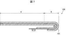
- the display device 100 disclosed in Patent Document 1 includes a display area A and a peripheral area B as shown in FIG.
- the peripheral region B is provided with a bent portion 101 for narrowing the frame, and the peripheral region B is bent at the bent portion 101.
- the wiring provided in the bent portion needs to be provided with, for example, a blank shape instead of a simple straight line, As a result, the resistance of the wiring is increased.
- One aspect of the present invention has been made in view of the above-described conventional problems, and an object of the present invention is to provide a display device that can reduce the resistance of a wiring even when the frame is narrowed. It is in.
- a display device includes a display region, a frame region having a bent portion and formed around the display region, and the bending in the frame region.
- An outer terminal portion having a first outer terminal portion and a second outer terminal portion provided in order from the display region side on the outer side opposite to the display region side from the portion; and the first outer terminal portion;
- a first routing wiring that electrically connects the internal wiring of the display region across the bent portion; an inner terminal portion provided inside the bent portion in the frame region; and the first outer terminal portion.
- at least the second outer terminal portion and the inner terminal portion of the second outer terminal portion are provided with a flexible second routing wiring that is electrically connected without passing through the bent portion.
- (A)-(l) is a top view which shows the shape of the 1st routing wiring of the said organic electroluminescence display. It is a top view which shows typically the whole structure of the organic electroluminescent display apparatus as a display device in Embodiment 2 of this invention. It is a top view which shows typically the whole structure of the organic electroluminescent display apparatus as a display device in Embodiment 3 of this invention. It is sectional drawing which shows the structure of the conventional display apparatus.
- FIG. 1 is a plan view schematically showing the overall configuration of an organic EL display device 1A of the present embodiment.
- An organic EL display device 1A as a display device of the present embodiment is a top emission type organic EL display device that emits light upward, and is connected to the display panel 40 and the display panel 40 as shown in FIG. And an electronic circuit board 50 made of a flexible substrate.
- the organic EL display device 1A is not necessarily a top emission type but may be a bottom emission type.
- the display panel 40 has a display area 41 and a frame area 42 provided around the display area 41.
- the frame region 42 is formed so that a part thereof protrudes on one side of the square display region 41. Further, in the present embodiment, for the purpose of narrowing the frame, a part of the protruding frame region 42 is folded back to the back side of the display region 41 at the bent portion 42a.
- FIG. 2 is a cross-sectional view showing the configuration of the organic EL display device 1A.
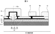
- FIG. 3 is a cross-sectional view illustrating a configuration of an end portion of the frame region 42 in the organic EL display device 1A.
- the display area 41 of the display panel 40 includes a base material 2, a resin layer 3, a barrier layer 4 (undercoat layer), a TFT (Thin Film Transistor) layer 10, and light emission in order from the bottom.
- the device layer 20, the sealing layer 30, the adhesive layer 5, and the functional film 6 are provided.
- Examples of the material of the substrate 2 include polyethylene terephthalate (PET).
- Examples of the material of the resin layer 3 include polyimide, epoxy, and polyamide.
- the barrier layer 4 is a layer that prevents moisture and impurities from reaching the TFT layer 10 and the light emitting element layer 20 when the display device is used.
- the barrier layer 4 can be composed of, for example, a silicon oxide film, a silicon nitride film, a silicon oxynitride film, or a stacked film thereof formed by CVD (Chemical Vapor Deposition).
- the TFT layer 10 is formed on the semiconductor film 11, the inorganic insulating film 12 formed above the semiconductor film 11, the gate electrode G formed above the inorganic insulating film 12, and the upper layer above the gate electrode G.
- the inorganic insulating film 13 is formed, the capacitor wiring (not shown) formed above the inorganic insulating film 13, the inorganic insulating film 14 formed above the capacitive wiring, and the upper layer than the inorganic insulating film 14.
- the semiconductor film 11, the inorganic insulating film 12 that is a gate insulating film, and the gate electrode G constitute a thin film transistor Td that functions as a light emission control transistor.
- the source electrode S is connected to the source region of the semiconductor film 11, and the drain electrode D is connected to the drain region of the semiconductor film 11.
- the semiconductor film 11 is made of, for example, low-temperature polysilicon (LTPS) or an oxide semiconductor.
- LTPS low-temperature polysilicon
- FIG. 2 the TFT having the semiconductor film 11 as a channel is shown as a top gate structure, but a bottom gate structure may be used.
- the TFT channel is an oxide semiconductor.
- the inorganic insulating films 12, 13, and 14 can be formed of, for example, a silicon oxide (SiOx) film, a silicon nitride (SiNx) film, or a stacked film thereof formed by a CVD method.
- the planarizing film 15 functions as an interlayer insulating film, and can be composed of a photosensitive organic material that can be applied, such as polyimide or acrylic.
- the gate electrode G, the source electrode S, the drain electrode D, and the terminal are, for example, aluminum (Al), tungsten (W), molybdenum (Mo), tantalum (Ta), chromium (Cr), titanium (Ti), copper (Cu ) Of a metal containing at least one of (1).
- the light emitting element layer 20 is composed of, for example, an organic light emitting diode layer, and an anode electrode 21 formed above the planarizing film 15 and a display area 41 that is an area overlapping the light emitting element layer 20.
- a pixel bank 22 defining sub-pixels; a light emitting layer 23 formed above the anode electrode 21; and a cathode electrode 24 formed above the light emitting layer 23.
- an organic light emitting diode (OLED) is configured to include the cathode electrode 24.
- the pixel bank 22 covers the edge of the anode electrode 21, and the light emitting layer 23 is formed in a light emitting region which is a region surrounded by the pixel bank 22 by a vapor deposition method or an ink jet method.
- the light emitting element layer 20 is an organic light emitting diode (OLED) layer, for example, a hole injection layer, a hole transport layer, a light emitting layer 23, an electron is formed on the bottom surface of the pixel bank 22, that is, the portion where the anode electrode 21 is exposed.
- a transport layer and an electron injection layer are stacked.
- a layer other than the light emitting layer 23 can be used as a common layer.
- the anode (anode) electrode 21 is composed of a laminate of, for example, ITO (Indium (Tin Oxide) and an alloy containing silver (Ag), and has light reflectivity.
- the cathode electrode 24 can be made of a light-transmitting conductive material such as ITO (Indium Tin Oxide) or IZO (Indium Zinc Oxide).
- the light-emitting element layer 20 is an OLED layer
- holes and electrons are recombined in the light-emitting layer 23 by the driving current between the anode electrode 21 and the cathode electrode 24, and the excitons generated thereby fall to the ground state.
- the cathode electrode 24 is light-transmitting and the anode electrode 21 is light-reflective, the light emitted from the light-emitting layer 23 is directed upward and becomes top emission.
- the light emitting element layer 20 is not limited to constituting an OLED element, and may constitute an inorganic light emitting diode or a quantum dot light emitting diode.
- a sealing layer 30 is formed on the light emitting element layer 20.
- the sealing layer 30 is translucent, and includes an inorganic sealing film 31 that covers the cathode electrode 24 of the light emitting element layer 20, an organic sealing film 32 that is formed above the inorganic sealing film 31, and organic sealing. And an inorganic sealing film 33 covering the film 32.
- the inorganic sealing films 31 and 33 can be composed of, for example, a silicon oxide film, a silicon nitride film, a silicon oxynitride film, or a stacked film thereof formed by CVD using a mask.
- the organic sealing film 32 is a light-transmitting organic film thicker than the inorganic sealing films 31 and 33, and can be composed of a photosensitive organic material that can be applied, such as polyimide or acrylic.
- a photosensitive organic material such as polyimide or acrylic.
- an ink containing such an organic material is applied onto the inorganic sealing film 31 by inkjet and then cured by UV irradiation.
- the sealing layer 30 covers the light emitting element layer 20 and prevents penetration of foreign matters such as water and oxygen into the light emitting element layer 20.
- the functional film 6 is, for example, a film having an optical compensation function, a touch sensor function, a protection function, and the like, and is adhered by the adhesive layer 5.
- a first routing wiring 43 extending from the internal wiring of the display area 41 is arranged at the end of the frame area 42 in the display panel 40.
- the first lead wiring 43 includes a lead wiring DW, a relay wiring LW, and a terminal wiring TW.
- the lead-out wiring DW is electrically connected to various internal wirings of the TFT layer 10 shown in FIG. Specifically, the lead-out wiring DW is connected to an internal wiring of the display area 41, for example, a source wiring (data wiring) provided in the display area 41 and connected to the source electrode S.
- a gate wiring (not shown) connected to the gate electrode G is connected to an IC chip 51 described later via the first outer terminal portion TM, the gate wiring is included in the internal wiring of the display region 41.
- the relay wiring LW is formed in the same process as the source electrode S, for example. Therefore, the relay wiring LW is formed on the inorganic insulating film 14 with the same material as the source electrode S. Specifically, the relay wiring LW and the source electrode S are formed of, for example, a two-layer titanium film and an aluminum film sanded thereon. The relay wiring LW is covered with the planarizing film 15. In the present embodiment, the bent portion 42a exists in the portion where the relay wiring LW is arranged.
- the terminal wiring TW is a wiring extending further from the relay wiring LW to the end of the frame area 42, and the first outer terminal portion TM is connected to the end.
- a planarizing film 15 covers a part on the upper side of the first outer terminal portion TM. Accordingly, the other part of the first outer terminal portion TM is exposed.
- the first outer terminal portion TM and the second outer terminal portion described later are provided in order from the display region 41 side on the outer side opposite to the display region 41 side than the bent portion 42a.
- the first terminal wiring 43 and a second wiring 63 described later are connected to each other.
- an electronic circuit board 50 and a flexible printed circuit (FPC) 60 are connected to the end of the frame region 42.
- FPC 60 is provided on the outermost side in the end portion of the frame region 42, and the electronic circuit board 50 is provided so as to partially cover the upper side of the end portion on the bent portion 42a side in the FPC 60.
- the electronic circuit board 50 and the FPC 60 are connected by a connecting portion 61a.
- an IC chip 51 is mounted on the electronic circuit board 50.
- the terminals of the IC chip 51 are connected to the first outer terminal portion TM, which is a part of the outer terminal portion, through an anisotropic conductive adhesive (ACF: Anisotropic Conductive ⁇ ⁇ ⁇ Film) (not shown).
- ACF Anisotropic Conductive ⁇ ⁇ ⁇ Film
- COF Chip On Film
- the FPC 60 is provided with a connector 62 as a second outer terminal portion, and this connector 62 is connected to the second routing wiring 63.
- the details of the second routing wiring 63 will be described later.
- the display panel 40 has flexibility.
- a bent portion 42a is provided in a frame region 42 that is a peripheral portion of the display panel 40, and the frame region 42 of the display panel 40 is bent at the bent portion 42a.
- the inorganic insulating films 13 and 14 and the like are removed, and the planarizing film 15 which is an organic film is filled.
- the electronic circuit board 50 and the FPC 60 are connected to the outside of the bent portion 42a in the display panel 40.
- the electronic circuit board 50 is provided with the IC chip 51 as an integrated circuit element for driving the display area 41 of the display panel 40 and mounted with a power supply semiconductor element (not shown). Yes.
- the first routing wiring 43 disposed between the display area 41 of the display panel 40 and the IC chip 51 is disposed so as to intersect the bent portion 42 a of the display panel 40. This is because in the first routing wiring 43, the number of output terminals in the data wiring connected to the first routing wiring 43 is large, so that the frame cannot be narrowed without bending.
- FIGS. 4A to 4L are plan views showing the shape of the first routing wiring 43 of the organic EL display device 1A.
- the first routing wiring 43 has many restrictions on the wiring shape in order to prevent disconnection at the bent portion 42a. For this reason, as shown in FIGS. 4A to 4L, the wiring 43a is not a simple straight wiring, but is formed in, for example, a wide, mesh-shaped or blank-shaped wiring 43a. As a result, the resistance of the first routing wiring 43 is increased. That is, the first routing wiring 43 is a high impedance wiring. Further, in the electronic circuit board 50 having the configuration of COF (Chip On Film), the crimp terminal portion tends to have a high resistance.
- COF Chip On Film
- a direct connection between the FPC 60 and the inner terminal portion 44 provided on the inner side of the bent portion 42a of the frame region 42 is provided.
- a second lead-out wiring 63 arranged in the circuit. That is, the second routing wiring 63 passes from the power supply semiconductor element (not shown) mounted on the FPC 60 to the inner terminal portion 44 through the connector 62 as the second outer terminal portion without passing through the bent portion 42 a of the frame region 42. It is connected.
- the second routing wiring 63 is arranged in the vicinity of the first routing wiring 43 and has a lower impedance than the first routing wiring 43.
- the second routing wiring 63 is configured using a part of the wiring of the FPC 60 and has flexibility.
- the second routing wiring 63 is not necessarily made of a flexible printed circuit board, and may be made of, for example, a covered wiring having flexibility. Thereby, when the frame area 42 is bent at the bent portion 42a, the second routing wiring 63 can also be flexibly bent while maintaining the insulating property.
- the second routing wiring 63 is a power supply voltage line (power supply line)
- the second routing wiring 63 is connected to, for example, the IC chip 51 on the electronic circuit board 50.
- the organic EL display device 1A having the bent portion 42a in the frame region 42 of the display panel 40 for narrowing the frame it is possible to prevent disconnection and reduce the total resistance of the wiring. It becomes.
- the first routing wiring 43 and the second routing wiring 63 such as a power supply line are different routes. As a result, it is possible to prevent noise from being mixed into the first routing wiring 43.
- the IC chip 51 as an integrated circuit element is provided on the electronic circuit board 50 made of COF.
- the total wiring of the organic EL display device 1A having the bent portion 42a in the frame region 42 of the display panel 40 for narrowing the frame is reduced. It is possible to provide the organic EL display device 1 ⁇ / b> A that can reduce the resistance and can prevent power consumption and display quality from being lowered.
- the second routing wiring 63 is described as being applied to a power supply line.
- the present invention is not necessarily limited to this, and the second routing wiring 63 can be used for other wiring with a small number of terminals.
- the second routing wiring 63 transmits the power supply wiring that transmits the above-described high power supply voltage or low power supply voltage, the wiring that transmits the clock signal, the wiring that transmits the start pulse signal, and the switching signal for time division driving. It is possible to apply to at least one of the wirings. Alternatively, it can be shared with the inspection terminal. For example, since a large current flows through a wiring that transmits a clock signal, it is desirable to reduce the resistance.
- the second routing wiring 63 applied other than the power supply line is connected from the FPC 60 to an external circuit (not shown) without being connected to the IC chip 51, for example.
- the inner terminal portion 44 provided inside the bent portion 42a in the frame region 42, and the connector as the first outer terminal portion TM and the second outer terminal portion.
- a flexible second routing wiring 63 is provided which electrically connects at least the connector 62 and the inner terminal portion 44 without passing through the bent portion 42a.
- the second routing wiring 63 is directly connected between at least the connector 62 and the inner terminal portion 44 provided on the inner side of the bent portion 42a in the frame region 42 without using the bent portion 42a. Connected.
- the organic EL display device 1A that can reduce the resistance of the wiring even when the frame is narrowed.
- the display region 41 is formed with a plurality of thin film transistors Td, a light emitting element layer 20, and a plurality of thin film transistors Td above and below the light emitting element layer 20.
- the planarizing film 15 is provided.
- the first routing wiring 43 is formed in an upper layer than the gate electrode G of the thin film transistor Td and in a lower layer than the planarizing film 15, or is formed in the same layer as the gate electrode G. As a result, the first lead wiring 43 can be formed in the same process as the internal wiring of the display area 41.
- the second routing wiring 63 is provided in the vicinity of the bent portion 42a. Therefore, since the first routing wiring 43 is routed in the bent portion 42a, the second routing wiring 63 and the first routing wiring 43 can be collectively arranged at positions near each other.
- the second routing wiring 63 is configured using a flexible printed circuit board. Thereby, the 2nd routing wiring 63 can be given flexibility, and bending becomes easy.
- an electronic circuit board 50 and an FPC 60 configured by COF (Chip On Film) are provided outside the bent portion 42a in the frame region 42.
- the first outer terminal portion TM of the first routing wiring 43 is connected to an IC chip 51 as an integrated circuit element mounted on the electronic circuit board 50, and the FPC 60 is an outer terminal connected to the second routing wiring 63. It has a connector 62 as a second outer terminal part which is a part of the part.
- the electronic circuit board 50 and the FPC 60 made of COF are provided outside the bent portion 42a in the frame region 42, the first routing wiring 43 and the second routing wiring 63 are respectively used for the purpose. Accordingly, it can be properly sorted and arranged.
- the second routing wiring 63 can supply a high power supply voltage or a low power supply voltage.
- the second routing wiring 63 can transmit at least one of a clock signal, a start pulse signal, and a time-division drive switching signal.
- the number of signal lines for transmitting the clock signal, the signal line for transmitting the start pulse signal, and the signal line for transmitting the switching signal for the time-division driving are respectively larger than the number of signal lines to the thin film transistor Td for each pixel in the display area 41. Therefore, it is possible to use a different route from the second routing wiring 63. As a result, at least one of the clock signal, the start pulse signal, and the time-division drive switching signal is transmitted through the second routing wiring 63, whereby the total resistance of the wiring can be reduced. As a result, it is possible to provide the organic EL display device 1A capable of reducing power consumption.
- the second routing wiring 63 has a lower resistance than the first routing wiring 43. As a result, it is possible to prevent disconnection of the total wiring and reduce resistance of the total wiring. As a result, it is possible to provide the organic EL display device 1A capable of reducing power consumption. In addition, this makes it possible to achieve both a narrow frame and low resistance.
- the organic EL display device 1A the IC chip 51 as an integrated circuit element is provided on the electronic circuit board 50.
- the organic EL display device 1B according to the present embodiment is different in that the IC chip 71 as an integrated circuit element is provided outside the bent portion 42a in the frame region 42 of the display panel 40. .
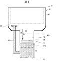
- FIG. 5 is a plan view schematically showing the configuration of the organic EL display device 1B of the present embodiment.
- the IC chip 71 as an integrated circuit element is provided outside the bent portion 42a in the frame region 42 of the display panel 40. Specifically, the IC chip 71 is directly mounted on the first outer terminal portion TM. As a result, the IC chip 71 is a so-called COP (Chip On Panel).
- COP Chip On Panel
- the FPC 60 having the connector 62 is connected to the outside of the bent portion 42a in the frame region 42 at the connection portion 61b, and the second routing wiring 63 is electrically connected to the connector 62. Yes.
- an organic EL display device 1B capable of reducing the total resistance of the wiring and thereby reducing power consumption is provided.
- Embodiment 3 The following will describe still another embodiment of the present invention with reference to FIG.
- the configurations other than those described in the present embodiment are the same as those in the first embodiment and the second embodiment.
- members having the same functions as those shown in the drawings of Embodiment 1 and Embodiment 2 are given the same reference numerals, and explanation thereof is omitted.
- the organic EL display device 1C as the display device in the present embodiment includes a plurality of inner terminal portions 44 inside the bent portion 42a in the frame region 42. The difference is that a plurality of second routing wires 63 are provided.
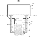
- FIG. 6 is a plan view schematically showing the configuration of the organic EL display device 1C of the present embodiment.
- the organic EL display device 1 ⁇ / b> C of the present embodiment is provided with a plurality of inner terminal portions 44 inside the bent portion 42 a in the frame region 42 and a plurality of second lead wirings 63.
- the second routing wiring 63 is connected to a plurality of inner terminal portions 44 from a plurality of locations of the FPC 60. Specifically, without passing the bent portion 42a of the frame region 42 from the left and right sides of the FPC 60 toward the two inner terminal portions 44a and 44b formed inside the bent portion 42a in the frame region 42 of the display panel 40. Second routing wirings 63 and 63 are provided.
- One second routing wiring 63 is electrically connected from the connector 62 which is the second outer terminal portion of the FPC 60 to the inner terminal portion 44a, and the other second routing wiring 63 is connected from the connector 62 of the FPC 60 to the inner terminal portion 44b. Until electrically connected.
- the second routing wirings 63 and 63 are lower impedance wiring than the first routing wiring 43 and have flexibility.
- the two inner terminal portions 44a and 44b and the second routing wirings 63 and 63 connected to the corresponding inner terminal portions 44a and 44b are provided, it is easy to reduce the total resistance of the wiring. As a result, it is possible to provide the organic EL display device 1C that can easily reduce the power consumption. Further, when a plurality of inner terminal portions 44a and 44b are provided, for example, the degree of freedom in designing the layout of wirings connected to the second routing wirings 63 and 63 can be increased. For this reason, there is a merit that wiring can be easily routed.
- the present invention is not necessarily limited to this, and in the organic EL display device 1B of Embodiment 2, a plurality of inner terminal portions 44 and second lead wirings 63 can be provided. That is, even in the type in which the IC chip 71 is directly provided in the frame region 42 of the display panel 40, a plurality of second routing wirings 63 such as the second routing wirings 63 and 63 can be provided.
- the organic EL display devices 1A to 1C as display devices have been described as examples.
- the display device in one embodiment of the present invention is not particularly limited as long as it is a display panel including a display element.
- the display element includes a display element whose brightness and transmittance are controlled by current and a display element whose brightness and transmittance are controlled by voltage.
- an electric current control display element an organic EL (Electro Luminescence) display device provided with OLED (Organic Light Emitting Diode) or an EL display device such as an inorganic EL display device provided with an inorganic light emitting diode,
- a voltage-controlled display element there is a liquid crystal display element or the like.
- the display device (organic EL display devices 1A to 1C) according to the first aspect of the present invention includes a display region 41, a frame region 42 having a bent portion 42a and formed around the display region 41, and the frame region. 42, a first outer terminal portion TM and a second outer terminal portion (connector 62) provided in order from the display region 41 side on the outer side opposite to the display region 41 side from the bent portion 42a.
- a first lead wire 43 that electrically connects the outer terminal portion having the first outer terminal portion TM and the internal wiring of the display region 41 across the bent portion 42a, and the bent portion in the frame region 42 Out of the inner terminal portion 44 provided inside the portion 42a, the first outer terminal portion TM, and the second outer terminal portion (connector 62), at least the second outer terminal portion (connector). It is characterized in that a second lead wirings 63 having flexibility are electrically connected without passing through the bent portion 42a motor 62) and the inner terminal portion 44.
- the display device is provided with a bent portion in the frame region and the frame region is bent at the bent portion in order to narrow the frame. Further, the first routing wiring arranged between the internal wiring in the display area and the first outer terminal portion is arranged so as to cross the bent portion in the frame area.
- the first lead-out wiring is formed in a wide width with many restrictions on the shape of the wiring in order to prevent disconnection at the bent portion, resulting in higher resistance of the wiring.
- an inner terminal portion is provided inside the bent portion in the frame region, and at least the second outer terminal portion and the second outer terminal portion among the first outer terminal portion and the second outer terminal portion.
- a flexible second routing wiring is provided in which the inner terminal portion is electrically connected without passing through the bent portion. That is, the second routing wiring is directly connected at least between the second outer terminal portion and the inner terminal portion provided inside the bent portion in the frame region without the bent portion.
- the display region 41 includes a plurality of thin film transistors Td, a plurality of light emitting elements (light emitting element layer 20), and the plurality of thin film transistors Td. And a planarizing film 15 formed in an upper layer and a lower layer than the plurality of light emitting elements (light emitting element layer 20), and the first routing wiring 43 is more than the gate electrode G of the thin film transistor Td. It may be formed in an upper layer and a lower layer than the planarizing film 15 or in the same layer as the gate electrode G.
- the first routing wiring can be formed in the same process as the internal wiring of the display area.
- the second routing wiring 63 is provided in the vicinity of the bent portion 42a.
- the second routing wiring and the first routing wiring can be collectively arranged in the vicinity of each other.
- the second routing wiring 63 may be configured using a flexible printed board.
- the electronic circuit board 50 and the flexible printed circuit 60 configured by COF (ChipCOn Film) are provided outside the bent portion 42a in the frame region 42.
- the first outer terminal portion TM is connected to an integrated circuit element (IC chip 51) mounted on the electronic circuit board 50, and the flexible printed circuit 60 includes the second outer terminal portion TM. It can be assumed that an outer terminal portion (connector 62) is provided.
- a 1st routing wiring and a 2nd routing wiring are each suitable according to the objective It can be arranged separately.
- a plurality of the inner terminal portions 44 may be provided.
- the second routing wiring 63 can supply a high power supply voltage or a low power supply voltage.
- a display device capable of reducing power consumption can be provided.
- the second routing wiring 63 can transmit a clock signal.
- the number of signal lines for transmitting a clock signal is smaller than the number of signal lines to the thin film transistors for each pixel in the display area, and can be a different path from the first routing wiring. As a result, the total resistance of the wiring can be reduced by transmitting the clock signal through the second routing wiring. As a result, a display device capable of reducing power consumption can be provided.
- the second lead wiring 63 can transmit a start pulse signal.
- the number of signal lines for transmitting the start pulse signal is smaller than the number of signal lines to the thin film transistor for each pixel in the display area, and can be a different path from the first routing wiring. As a result, the resistance of the total wiring can be reduced by transmitting the start pulse signal through the second routing wiring. As a result, a display device capable of reducing power consumption can be provided.
- the second routing wiring 63 can transmit a switching signal for time division driving.
- the number of signal lines for transmitting the time division drive switching signal is smaller than the number of signal lines to the thin film transistor for each pixel in the display area, and can be a different path from the first routing wiring. As a result, the total resistance of the wiring can be reduced by transmitting the switching signal for the time division drive through the second routing wiring. As a result, a display device capable of reducing power consumption can be provided.
- the second routing wiring 63 has a lower resistance than the first routing wiring 43.
- the first routing wiring 43 can transmit a data signal.
- the data signal to the pixels in the display area can be transmitted by the first routing wiring.
- 1A to 1C organic EL display device (display device) 10 TFT layer 15 Planarizing film 20 Light emitting element layer (multiple light emitting elements) 23 Light emitting layer 30 Sealing layer 40 Display panel 41 Display area 42 Frame area 42a Bending part 43 First routing wiring 44 Inner terminal parts 44a and 44b Inner terminal part 50 Electronic circuit board 51 IC chip 60 Flexible printed circuit (FPC) 61a connection portion 61b connection portion 62 connector (second outer terminal portion) 63 Second lead wiring 71 IC chip DW Lead wiring (first lead wiring) LW relay wiring (first routing wiring) TW terminal wiring (first routing wiring) TM First outer terminal part (outer terminal part, first routing wiring) Td thin film transistor
Landscapes
- Engineering & Computer Science (AREA)
- Physics & Mathematics (AREA)
- Microelectronics & Electronic Packaging (AREA)
- Theoretical Computer Science (AREA)
- General Physics & Mathematics (AREA)
- Nonlinear Science (AREA)
- Computer Hardware Design (AREA)
- General Engineering & Computer Science (AREA)
- Human Computer Interaction (AREA)
- Mathematical Physics (AREA)
- Chemical & Material Sciences (AREA)
- Crystallography & Structural Chemistry (AREA)
- Optics & Photonics (AREA)
- Electroluminescent Light Sources (AREA)
- Devices For Indicating Variable Information By Combining Individual Elements (AREA)
Abstract
狭額縁化を図った場合においても、配線の低抵抗化を可能とする表示デバイスを提供する。有機EL表示装置(1A)は、表示領域(41)と、折り曲げ部(42a)を有し、かつ表示領域(41)の周囲に形成された額縁領域(42)と、額縁領域(42)において、折り曲げ部(42a)よりも表示領域(41)側とは反対側である外側に表示領域(41)側から順に設けられた第1外側端子部(TM)及びコネクタ(62)を有する外側端子部と、第1外側端子部(TM)と表示領域(41)の内部配線とを、折り曲げ部(42a)と交差して電気的に接続する第1引き回し配線(43)と、額縁領域(42)における折り曲げ部(42a)の内側に設けられた内側端子部(44)と、第1外側端子部(TM)及びコネクタ62のうち、少なくともコネクタ(62)と内側端子部(44)とを折り曲げ部(42a)を通ることなく電気的に接続した可撓性を有する第2引き回し配線(63)とを備えている。
Description
本発明は、狭額縁化のために額縁領域に折り曲げ部を有する表示デバイスに関するものである。
例えば、特許文献1に開示された表示装置100は、図7に示すように、表示領域Aと周辺領域Bとを有している。周辺領域Bには狭額縁化のために折り曲げ部101が設けられており、これによって、周辺領域Bは折り曲げ部101にて折り曲げられている。
しかしながら、従来の表示装置においては、折り曲げ部での断線を防ぐため、周知のように、該折り曲げ部に設けられる配線において、単純な直線の配線ではなく、例えば抜き形状などを設ける必要があり、結果として配線の高抵抗化に繋がっている。
本発明の一態様は、前記従来の問題点に鑑みなされたものであって、その目的は、狭額縁化を図った場合においても、配線の低抵抗化を可能とする表示デバイスを提供することにある。
本発明の一態様における表示デバイスは、前記の課題を解決するために、表示領域と、折り曲げ部を有し、かつ前記表示領域の周囲に形成された額縁領域と、前記額縁領域において、前記折り曲げ部よりも前記表示領域側とは反対側である外側に、前記表示領域側から順に設けられた第1外側端子部及び第2外側端子部を有する外側端子部と、前記第1外側端子部と前記表示領域の内部配線とを、前記折り曲げ部と交差して電気的に接続する第1引き回し配線と、前記額縁領域における折り曲げ部の内側に設けられた内側端子部と、前記第1外側端子部及び前記第2外側端子部のうち、少なくとも前記第2外側端子部と前記内側端子部とを前記折り曲げ部を通ることなく電気的に接続した可撓性を有する第2引き回し配線とを備えていることを特徴としている。
本発明の一態様によれば、狭額縁化を図った場合においても、配線の低抵抗化を可能とする表示デバイスを提供するという効果を奏する。
〔実施の形態1〕
本発明の一実施形態について図1~図3に基づいて説明すれば、以下のとおりである。
本発明の一実施形態について図1~図3に基づいて説明すれば、以下のとおりである。
本実施の形態の表示デバイスとしての例えば有機EL表示装置1Aの全体構成について、図1に基づいて説明する。図1は、本実施の形態の有機EL表示装置1Aの全体構成を模式的に示す平面図である。
本実施の形態の表示デバイスとしての有機EL表示装置1Aは、上方に向けて発光するトップエミッション型の有機EL表示装置であり、図1に示すように、表示パネル40と、表示パネル40に接続されたフレキシブル基板からなる電子回路基板50とを備えている。尚、有機EL表示装置1Aは、必ずしもトップエミッション型でなく、ボトムエミッション型であってもよい。
表示パネル40は、表示領域41と、該表示領域41の周囲に設けられた額縁領域42とを有している。額縁領域42は、例えば、方形の表示領域41の一辺側において一部が張り出すように形成されている。また、本実施の形態では、狭額縁化のため、張り出された額縁領域42の一部が折り曲げ部42aにて、表示領域41の裏面側に折り返されるようになっている。
有機EL表示装置1Aの表示パネル40の断面構造について、図2及び図3に基づいて説明する。図2は、有機EL表示装置1Aの構成を示す断面図である。図3は、有機EL表示装置1Aにおける額縁領域42の端部の構成を示す断面図である。
図2に示すように、表示パネル40の表示領域41は、下側から順に、基材2、樹脂層3、バリア層4(アンダーコート層)、TFT(Thin Film Transistor:薄膜トランジスタ)層10、発光素子層20、封止層30、接着層5及び機能フィルム6を備えている。
基材2の材料としては、例えばポリエチレンテレフタレート(PET)が挙げられる。また、樹脂層3の材料としては、例えば、ポリイミド、エポキシ、ポリアミド等が挙げられる。
バリア層4は、表示デバイスの使用時に、水分や不純物が、TFT層10や発光素子層20に到達することを防ぐ層である。バリア層4は、例えば、CVD(Chemical Vapor Deposition:化学気相成長法)により形成される酸化シリコン膜、窒化シリコン膜、若しくは酸窒化シリコン膜、又はこれらの積層膜で構成することができる。
TFT層10は、半導体膜11と、半導体膜11よりも上層に形成される無機絶縁膜12と、無機絶縁膜12よりも上層に形成されるゲート電極Gと、ゲート電極Gよりも上層に形成される無機絶縁膜13と、無機絶縁膜13よりも上層に形成される図示しない容量配線と、容量配線よりも上層に形成される無機絶縁膜14と、無機絶縁膜14よりも上層に形成されるソース電極S及びドレイン電極Dと、ソース電極S及びドレイン電極Dよりも上層に形成される平坦化膜15とを含んでいる。
前記半導体膜11、ゲート絶縁膜である無機絶縁膜12及びゲート電極Gによって、発光制御トランジスタとして機能する薄膜トランジスタTdが構成されている。ソース電極Sは半導体膜11のソース領域に接続され、ドレイン電極Dは半導体膜11のドレイン領域に接続されている。
半導体膜11は、例えば低温ポリシリコン(LTPS)又は酸化物半導体で構成される。尚、図2では、半導体膜11をチャネルとするTFTがトップゲート構造で示されているが、ボトムゲート構造でもよい。例えば、TFTのチャネルが酸化物半導体の場合である。
無機絶縁膜12・13・14は、例えば、CVD法によって形成された酸化シリコン(SiOx)膜若しくは窒化シリコン(SiNx)膜又はこれらの積層膜によって構成することができる。平坦化膜15は、層間絶縁膜として機能し、例えばポリイミド、アクリル等の塗布可能な感光性有機材料によって構成することができる。
ゲート電極G、ソース電極S、ドレイン電極D及び端子は、例えば、アルミニウム(Al)、タングステン(W)、モリブデン(Mo)、タンタル(Ta)、クロム(Cr)、チタン(Ti)、銅(Cu)の少なくとも1つを含む金属の単層膜又は積層膜によって構成されている。
発光素子層20は、本実施の形態では、例えば有機発光ダイオード層にてなり、平坦化膜15よりも上層に形成されるアノード電極21と、発光素子層20と重なる領域である表示領域41のサブ画素を規定する画素バンク22と、アノード電極21よりも上層に形成される発光層23と、発光層23よりも上層に形成されるカソード電極24とを含み、アノード電極21、発光層23、及びカソード電極24を含むように、例えば有機発光ダイオード(OLED)が構成される。
画素バンク22はアノード電極21のエッジを覆っており、発光層23は、蒸着法又はインクジェット法によって、画素バンク22で囲まれた領域である発光領域に形成される。発光素子層20が有機発光ダイオード(OLED)層である場合、画素バンク22の底面つまりアノード電極21が露出した部分上には、例えば、正孔注入層、正孔輸送層、発光層23、電子輸送層及び電子注入層が積層される。ここでは、発光層23以外を共通層とすることができる。
アノード(陽極)電極21は、例えばITO(Indium Tin Oxide)と銀(Ag)を含む合金との積層によって構成され、光反射性を有する。カソード電極24は、ITO(Indium Tin Oxide)又はIZO(Indium Zinc Oxide)等の透光性の導電材で構成することができる。
発光素子層20がOLED層である場合、アノード電極21及びカソード電極24の間の駆動電流によって正孔と電子とが発光層23内で再結合し、これによって生じたエキシトンが基底状態に落ちることによって、光が放出される。カソード電極24が透光性であり、アノード電極21が光反射性であるため、発光層23から放出された光は上方に向かい、トップエミッションとなる。
発光素子層20は、OLED素子を構成する場合に限られず、無機発光ダイオード又は量子ドット発光ダイオードを構成してもよい。
前記発光素子層20の上側には、封止層30が形成されている。封止層30は透光性であり、発光素子層20のカソード電極24を覆う無機封止膜31と、無機封止膜31よりも上層に形成される有機封止膜32と、有機封止膜32を覆う無機封止膜33とを含む。
無機封止膜31・33は、例えば、マスクを用いたCVDにより形成される酸化シリコン膜、窒化シリコン膜若しくは酸窒化シリコン膜、又はこれらの積層膜で構成することができる。
有機封止膜32は、無機封止膜31・33よりも厚い透光性有機膜であり、ポリイミド、アクリル等の塗布可能な感光性有機材料によって構成することができる。例えば、このような有機材料を含むインクを無機封止膜31上にインクジェット塗布した後、UV照射により硬化させる。
これにより、封止層30は、発光素子層20を覆い、水、酸素等の異物の発光素子層20への浸透を防いでいる。
機能フィルム6は、例えば、光学補償機能、タッチセンサ機能、保護機能等を有するフィルムであり、接着層5により接着される。
次に、表示パネル40における額縁領域42の端部には、図3に示すように、表示領域41の内部配線から延びる第1引き回し配線43が配されている。第1引き回し配線43は、引き出し配線DW、中継配線LW及び端子配線TWを含む。
引き出し配線DWは、図2に示すTFT層10の各種の内部配線と電気的に接続される。具体的には、引き出し配線DWは、表示領域41の内部配線、例えば、表示領域41に設けられかつソース電極Sに接続されたソース配線(データ配線)に接続されている。尚、ゲート電極Gに接続された図示しないゲート配線が第1外側端子部TMを介して後述するICチップ51に接続される場合には、該ゲート配線は表示領域41の内部配線に含まれる。
中継配線LWは、例えばソース電極Sと同一工程で形成される。このため、中継配線LWは、無機絶縁膜14上にソース電極Sと同材料にて形成される。具体的には、中継配線LW及びソース電極Sは、例えば、2層のチタン膜及びこれらにサンドされたアルミニウム膜にて形成される。また、中継配線LWは、平坦化膜15で覆われている。本実施の形態では、中継配線LWが配されている部分に折り曲げ部42aが存在する。
端子配線TWは、中継配線LWからさらに額縁領域42の末端に延びる配線であり、末端には第1外側端子部TMが接続されている。第1外側端子部TMの上側における一部には、平坦化膜15が覆っている。したがって、第1外側端子部TMの他の一部は露出している。
また、額縁領域42では、折り曲げ部42aよりも表示領域41側とは反対側である外側に、表示領域41側から順に設けられた上記第1外側端子部TM及び後述の第2外側端子部を有する外側端子部が設けられており、第1引き回し配線43及び後述の第2引き回し配線63が接続されている。
図1に示すように、本実施の形態では、額縁領域42の端部には、電子回路基板50とフレキシブルプリント回路(Flexible Printed Circuits:FPC)60(以下、「FPC60」という。)とが接続されている。FPC60が額縁領域42の端部における最も外側に設けられていると共に、FPC60における折り曲げ部42a側の端部の上側を一部覆うようにして電子回路基板50が設けられている。前記電子回路基板50とFPC60とは、接続部61aにて接続されている。
電子回路基板50には、例えばICチップ51が搭載されている。ICチップ51の端子は、図示しない異方性導電接着剤(ACF:Anisotropic Conductive Film)を介して外側端子部の一部である上記第1外側端子部TMに接続されている。この結果、電子回路基板50は、所謂COF(Chip On Film)の構成を有している。
FPC60には、第2外側端子部としてのコネクタ62が設けられており、このコネクタ62は、第2引き回し配線63に接続されている。尚、第2引き回し配線63の詳細については後述する。
本実施の形態の有機EL表示装置1Aでは、表示パネル40が可撓性を有している。そして、狭額縁化のため、表示パネル40の周囲部である額縁領域42に折り曲げ部42aが設けられており、この折り曲げ部42aにて表示パネル40の額縁領域42を折曲している。折り曲げ部42aでは、折り曲げ加工を容易に行うために、図3に示すように、無機絶縁膜13・14等が除去され、有機膜である平坦化膜15が充填されている。さらに、表示パネル40における折り曲げ部42aよりも外側には、前述したように、電子回路基板50及びFPC60が接続されている。
上記電子回路基板50には、前述したように、表示パネル40の表示領域41を駆動する集積回路素子としてのICチップ51が設けられていると共に、図示しない電源供給用半導体素子等が実装されている。
この結果、表示パネル40の表示領域41とICチップ51との間に配される第1引き回し配線43は、表示パネル40の折り曲げ部42aを交差して配されている。この理由は、第1引き回し配線43では、該第1引き回し配線43に接続されたデータ配線における出力端子の数が多いので、折曲しないと狭額縁化できないためである。
ここで、第1引き回し配線43の配線形状について、図4の(a)~(l)に基づいて説明する。図4の(a)~(l)は、有機EL表示装置1Aの第1引き回し配線43の形状を示す平面図である。
本実施の形態の有機EL表示装置1Aでは、第1引き回し配線43は、折り曲げ部42aでの断線を防ぐため、配線形状に制約が多い。このため、図4の(a)~(l)に示すように、単純な直線配線ではなく、例えば、幅広、網目状又は抜き形状の配線43aに形成されている。この結果、第1引き回し配線43の高抵抗化を招くものとなっている。つまり、第1引き回し配線43は、高インピーダンス配線となっている。また、COF(Chip On Film)の構成を有する電子回路基板50においては、圧着端子部において高抵抗になる傾向がある。
一方、端子数が少なくてもよい電源供給線等は接続領域が小さくて済むため、折り曲げ部42aを介さなくても狭額縁化を損なわない。また、電源供給線は、抵抗が大きいと電力を特に消費する。
そこで、本実施の形態の有機EL表示装置1Aにおいては、図1に示すように、FPC60と、額縁領域42の折り曲げ部42aよりも内側に設けられた内側端子部44との間を、直接的に配される第2引き回し配線63にて接続している。すなわち、第2引き回し配線63は、額縁領域42の折り曲げ部42aを通さずに、FPC60に搭載された図示しない電源供給用半導体素子から第2外側端子部としてのコネクタ62を経て内側端子部44まで接続されている。第2引き回し配線63は、第1引き回し配線43の近傍に配されており、かつ第1引き回し配線43よりも低インピーダンスの配線となっている。また、第2引き回し配線63は、FPC60の一部の配線を用いて構成されており、フレキシブル性を有している。尚、第2引き回し配線63は、必ずしもフレキシブルプリント基板からなっている必要はなく、フレキシブル性を有する例えば被覆配線からなっていてもよい。これにより、額縁領域42を折り曲げ部42aにて折り曲げたときに、第2引き回し配線63も絶縁性を保持して柔軟に曲げることができる。
また、第2引き回し配線63が電源電圧線(電源供給線)である場合には、第2引き回し配線63は、例えば、電子回路基板50上のICチップ51に接続される。
この結果、狭額縁化のために表示パネル40の額縁領域42に折り曲げ部42aを有する有機EL表示装置1Aにおいて、断線の発生を防止すると共に、配線のトータル的な低抵抗化を図ることが可能となる。延いては、消費電力の低減、及び表示品質の低下を防止し得る有機EL表示装置1Aを提供することができる。すなわち、高抵抗の場合、電圧低下幅が大きくなり、発光量変動が大きい。この結果、表示品質の低下を招く。
また、本実施の形態では、第1引き回し配線43と電源供給線等の第2引き回し配線63とは別ルートの配線となる。この結果、第1引き回し配線43にノイズが混入することを防止することができる。
また、本実施の形態の有機EL表示装置1Aでは、集積回路素子としてのICチップ51は、COFからなる電子回路基板50に設けられている。これにより、ICチップ51が電子回路基板50に設けられている場合に、狭額縁化のために表示パネル40の額縁領域42に折り曲げ部42aを有する有機EL表示装置1Aにおいて、配線のトータル的な低抵抗化を図り、延いては、消費電力の低減、及び表示品質の低下を防止し得る有機EL表示装置1Aを提供することができる。
尚、本実施の形態では、第2引き回し配線63は、電源供給線に適用されるとして説明した。しかし、本発明の一態様においては、必ずしもこれに限らず、第2引き回し配線63は、端子数が少ない他の配線に使用することが可能である。例えば、第2引き回し配線63は、前述した高電源電圧又は低電源電圧を伝達する電源供給配線、クロック信号を伝達する配線、スタートパルス信号を伝達する配線、及び時分割駆動の切替信号を伝達する配線の少なくとも一つに適用することが可能である。或いは、検査端子と共用することも可能である。例えばクロック信号を伝達する配線は、大きな電流が流れるので、低抵抗化が望ましい。尚、電源供給線以外に適用された第2引き回し配線63は、例えばICチップ51に接続されることなく、FPC60から図示しない外部回路に接続される。
このように、本実施の形態の有機EL表示装置1Aでは、額縁領域42における折り曲げ部42aの内側に設けられた内側端子部44と、第1外側端子部TM及び第2外側端子部としてのコネクタ62のうち、少なくともコネクタ62と内側端子部44とを折り曲げ部42aを通ることなく電気的に接続した可撓性を有する第2引き回し配線63とを備えている。すなわち、本実施の形態では、第2引き回し配線63は、少なくともコネクタ62と、額縁領域42における折り曲げ部42aの内側に設けられた内側端子部44との間を、折り曲げ部42aを介さずに直接接続される。
この結果、狭額縁化を図った場合においても、配線の低抵抗化を可能とする有機EL表示装置1Aを提供することができる。
また、本実施の形態における有機EL表示装置1Aでは、表示領域41には、複数の薄膜トランジスタTdと、発光素子層20と、複数の薄膜トランジスタTdよりも上層かつ発光素子層20よりも下層に形成された平坦化膜15とが設けられている。そして、第1引き回し配線43は、薄膜トランジスタTdのゲート電極Gよりも上層かつ平坦化膜15よりも下層に形成されているか、又は前記ゲート電極Gと同層に形成されている。これにより、第1引き回し配線43を表示領域41の内部配線と同一工程で形成することができる。
また、本実施の形態における有機EL表示装置1Aでは、第2引き回し配線63は、折り曲げ部42aの近傍に設けられている。これにより、折り曲げ部42aには第1引き回し配線43が引き回されているので、第2引き回し配線63及び第1引き回し配線43を互いの近傍位置にまとめて配設することができる。
また、本実施の形態における有機EL表示装置1Aでは、第2引き回し配線63は、フレキシブルプリント基板を用いて構成されている。これにより、第2引き回し配線63にフレキシブル性を持たせることができ、折り曲げが容易となる。
また、本実施の形態における有機EL表示装置1Aでは、額縁領域42における折り曲げ部42aの外側には、COF(Chip On Film)にて構成される電子回路基板50とFPC60とが設けられている。第1引き回し配線43の第1外側端子部TMは、電子回路基板50に搭載された集積回路素子としてのICチップ51に接続されており、FPC60は、第2引き回し配線63に接続される外側端子部の一部である第2外側端子部としてのコネクタ62を有している。
これにより、額縁領域42における折り曲げ部42aの外側に、COFにて構成される電子回路基板50とFPC60とが設けられている場合に、第1引き回し配線43及び第2引き回し配線63をそれぞれ目的に応じて適切に分別して配設することができる。
また、本実施の形態における有機EL表示装置1Aでは、第2引き回し配線63は、高電源電圧又は低電源電圧を供給するとすることができる。
高電源電圧又は低電源電圧は、低インピーダンスに供給することが好ましい。この結果、高電源電圧又は低電源電圧を第2引き回し配線63にて供給することによって、トータル的な配線の断線防止、及びトータル的な配線の低抵抗化を図ることができる。延いては、消費電力の低減、及び表示品質の低下を防止し得る有機EL表示装置1Aを提供することができる。
また、本実施の形態における有機EL表示装置1Aでは、第2引き回し配線63は、クロック信号、スタートパルス信号及び時分割駆動の切替信号のいずれか少なくとも1つを伝達するとすることができる。
クロック信号を伝達する信号線、スタートパルス信号を伝達する信号線、及び時分割駆動の切替信号を伝達する信号線は、それぞれ、表示領域41の画素毎の薄膜トランジスタTdへの信号線に比べて本数が少なく、第2引き回し配線63とは別経路とすることが可能である。この結果、クロック信号、スタートパルス信号及び時分割駆動の切替信号のいずれか少なくとも1つを第2引き回し配線63にて伝達することによって、トータル的な配線の低抵抗化を図ることができる。延いては、消費電力の低減を図り得る有機EL表示装置1Aを提供することができる。
また、本実施の形態における有機EL表示装置1Aでは、第2引き回し配線63は、第1引き回し配線43よりも低抵抗である。これにより、トータル的な配線の断線防止、及びトータル的な配線の低抵抗化を図ることができる。延いては、消費電力の低減を図り得る有機EL表示装置1Aを提供することができる。また、これにより、狭額縁と低抵抗化とを両立することができる。
〔実施の形態2〕
本発明の他の実施の形態について図5に基づいて説明すれば、以下のとおりである。尚、本実施の形態において説明すること以外の構成は、前記実施の形態1と同じである。また、説明の便宜上、前記の実施の形態1の図面に示した部材と同一の機能を有する部材については、同一の符号を付し、その説明を省略する。
本発明の他の実施の形態について図5に基づいて説明すれば、以下のとおりである。尚、本実施の形態において説明すること以外の構成は、前記実施の形態1と同じである。また、説明の便宜上、前記の実施の形態1の図面に示した部材と同一の機能を有する部材については、同一の符号を付し、その説明を省略する。
前記実施の形態1における有機EL表示装置1Aでは、集積回路素子としてのICチップ51は、電子回路基板50に設けられていた。これに対して、本実施の形態における有機EL表示装置1Bでは、集積回路素子としてのICチップ71は、表示パネル40の額縁領域42における折り曲げ部42aの外側に設けられている点が異なっている。
本実施の形態の表示デバイスとしての有機EL表示装置1Bの構成について、図5に基づいて説明する。図5は、本実施の形態の有機EL表示装置1Bの構成を模式的に示す平面図である。
本実施の形態の有機EL表示装置1Bでは、図5に示すように、集積回路素子としてのICチップ71は、表示パネル40の額縁領域42における折り曲げ部42aの外側に設けられている。具体的には、ICチップ71は、第1外側端子部TMに直接的に実装されている。この結果、ICチップ71は、所謂COP(Chip On Panel)となっている。
また、本実施の形態では、コネクタ62を有するFPC60は、接続部61bにて額縁領域42における折り曲げ部42aの外側で接続されており、第2引き回し配線63はコネクタ62に電気的に接続されている。
この構成により、ICチップ71が、表示パネル40の額縁領域42における折り曲げ部42aの外側に設けられている場合に、狭額縁化のために表示パネル40の額縁領域42に折り曲げ部42aを有する有機EL表示装置1Bにおいて、配線のトータル的な低抵抗化を図り、延いては、消費電力の低減を図り得る有機EL表示装置1Bを提供するものとなっている。
〔実施の形態3〕
本発明のさらに他の実施の形態について図6に基づいて説明すれば、以下のとおりである。尚、本実施の形態において説明すること以外の構成は、前記実施の形態1及び実施の形態2と同じである。また、説明の便宜上、前記の実施の形態1及び実施の形態2の図面に示した部材と同一の機能を有する部材については、同一の符号を付し、その説明を省略する。
本発明のさらに他の実施の形態について図6に基づいて説明すれば、以下のとおりである。尚、本実施の形態において説明すること以外の構成は、前記実施の形態1及び実施の形態2と同じである。また、説明の便宜上、前記の実施の形態1及び実施の形態2の図面に示した部材と同一の機能を有する部材については、同一の符号を付し、その説明を省略する。
本実施の形態における表示デバイスとしての有機EL表示装置1Cは、実施の形態1の有機EL表示装置1Aの構成に加えて、額縁領域42における折り曲げ部42aの内側に内側端子部44が複数設けられ、第2引き回し配線63が複数設けられている点が異なっている。
本実施の形態における表示デバイスとしての有機EL表示装置1Cの構成について、図6に基づいて説明する。図6は、本実施の形態の有機EL表示装置1Cの構成を模式的に示す平面図である。
本実施の形態の有機EL表示装置1Cは、図6に示すように、額縁領域42における折り曲げ部42aの内側に内側端子部44が複数設けられ、かつ第2引き回し配線63が複数設けられている。換言すれば、第2引き回し配線63は、FPC60の複数箇所から複数の内側端子部44に接続されている。具体的には、FPC60の左右の両側から表示パネル40の額縁領域42における折り曲げ部42aの内側に形成された2つの内側端子部44a・44bに向けて額縁領域42の折り曲げ部42aを通さずに配される第2引き回し配線63・63が設けられている。一方の第2引き回し配線63はFPC60の第2外側端子部であるコネクタ62から内側端子部44aまで電気的に接続されており、他方の第2引き回し配線63はFPC60のコネクタ62から内側端子部44bまで電気的に接続されている。第2引き回し配線63・63は、第1引き回し配線43よりも低インピーダンスの配線となっていると共に、フレキシブル性を有している。
このように2つの内側端子部44a・44bと、対応する内側端子部44a・44bに接続された第2引き回し配線63・63が設けられているので、配線のトータル的な低抵抗化を容易に図り、延いては、消費電力の低減を簡単に図り得る有機EL表示装置1Cを提供することができる。また、複数の内側端子部44a・44bを設ける場合には、例えば、第2引き回し配線63・63に接続される配線のレイアウトについての設計自由度を大きくすることができる。このため、配線の引き回しを容易に行うことができるというメリットがある。
尚、本実施の形態では、実施の形態1の有機EL表示装置1Aにおいて、第2引き回し配線63が複数設けられている点について説明した。しかし、本発明の一態様においては、必ずしもこれに限らず、実施の形態2の有機EL表示装置1Bにおいても、内側端子部44及び第2引き回し配線63を複数設けることが可能である。すなわち、ICチップ71が、表示パネル40の額縁領域42に直接設けられているタイプにおいても、第2引き回し配線63・63のように第2引き回し配線63を複数設けることが可能である。
また、実施の形態1~3では、表示デバイスとしての有機EL表示装置1A~1Cを例示して説明した。しかし、本発明の一態様における表示デバイスは、表示素子を備えた表示パネルであれば、特に限定されるものではない。前記表示素子には、電流によって輝度や透過率が制御される表示素子と、電圧によって輝度や透過率が制御される表示素子とがある。電流制御の表示素子としては、OLED(Organic Light Emitting Diode:有機発光ダイオード)を備えた有機EL(Electro Luminescence:エレクトロルミネッセンス)表示装置若しくは無機発光ダイオードを備えた無機EL表示装置等のEL表示装置、又はQLED(Quantum dot Light Emitting Diode:量子ドット発光ダイオード)を備えたQLED表示装置等がある。また、電圧制御の表示素子としては、液晶表示素子等がある。
〔まとめ〕
本発明の態様1における表示デバイス(有機EL表示装置1A~1C)は、表示領域41と、折り曲げ部42aを有し、かつ前記表示領域41の周囲に形成された額縁領域42と、前記額縁領域42において、前記折り曲げ部42aよりも前記表示領域41側とは反対側である外側に、前記表示領域41側から順に設けられた第1外側端子部TM及び第2外側端子部(コネクタ62)を有する外側端子部と、前記第1外側端子部TMと前記表示領域41の内部配線とを、前記折り曲げ部42aと交差して電気的に接続する第1引き回し配線43と、前記額縁領域42における折り曲げ部42aの内側に設けられた内側端子部44と、前記第1外側端子部TM及び第2外側端子部(コネクタ62)のうち、少なくとも前記第2外側端子部(コネクタ62)と前記内側端子部44とを前記折り曲げ部42aを通ることなく電気的に接続した可撓性を有する第2引き回し配線63とを備えていることを特徴としている。
本発明の態様1における表示デバイス(有機EL表示装置1A~1C)は、表示領域41と、折り曲げ部42aを有し、かつ前記表示領域41の周囲に形成された額縁領域42と、前記額縁領域42において、前記折り曲げ部42aよりも前記表示領域41側とは反対側である外側に、前記表示領域41側から順に設けられた第1外側端子部TM及び第2外側端子部(コネクタ62)を有する外側端子部と、前記第1外側端子部TMと前記表示領域41の内部配線とを、前記折り曲げ部42aと交差して電気的に接続する第1引き回し配線43と、前記額縁領域42における折り曲げ部42aの内側に設けられた内側端子部44と、前記第1外側端子部TM及び第2外側端子部(コネクタ62)のうち、少なくとも前記第2外側端子部(コネクタ62)と前記内側端子部44とを前記折り曲げ部42aを通ることなく電気的に接続した可撓性を有する第2引き回し配線63とを備えていることを特徴としている。
前記構成によれば、表示デバイスは、狭額縁化のため、額縁領域に折り曲げ部を設けて額縁領域を折り曲げ部にて折り曲げている。また、表示領域の内部配線と第1外側端子部との間に配される第1引き回し配線は、額縁領域の折り曲げ部を交差して配されている。
この種の表示デバイスでは、第1引き回し配線は、折り曲げ部での断線を防ぐため、配線形状に制約が多く幅広等に形成するので、結果として配線の高抵抗化に繋がっている。
一方、端子数が少なくてもよい電源供給線等は接続領域が小さくて済むため、折り曲げ部を介さなくても狭額縁化を損なわない。
そこで、本発明の一態様においては、額縁領域における折り曲げ部の内側には内側端子部が設けられていると共に、第1外側端子部及び第2外側端子部のうち、少なくとも第2外側端子部と内側端子部とを折り曲げ部を通ることなく電気的に接続した可撓性を有する第2引き回し配線を備えている。すなわち、第2引き回し配線は、少なくとも第2外側端子部と、額縁領域における折り曲げ部の内側に設けられた内側端子部との間を、折り曲げ部を介さずに直接接続される。
この結果、狭額縁化を図った場合においても、配線の低抵抗化を可能とする表示デバイスを提供することができる。
本発明の態様2における表示デバイス(有機EL表示装置1A~1C)では、前記表示領域41には、複数の薄膜トランジスタTdと、複数の発光素子(発光素子層20)と、前記複数の薄膜トランジスタTdよりも上層かつ前記複数の発光素子(発光素子層20)よりも下層に形成された平坦化膜15とが設けられていると共に、前記第1引き回し配線43は、前記薄膜トランジスタTdのゲート電極Gよりも上層かつ前記平坦化膜15よりも下層に形成されているか、又は前記ゲート電極Gと同層に形成されているとすることができる。
これにより、第1引き回し配線を表示領域の内部配線と同一工程で形成することができる。
本発明の態様3における表示デバイス(有機EL表示装置1A~1C)では、前記第2引き回し配線63は、前記折り曲げ部42aの近傍に設けられていることが好ましい。
これにより、折り曲げ部には第1引き回し配線が引き回されているので、第2引き回し配線及び第1引き回し配線を互いの近傍位置にまとめて配設することができる。
本発明の態様4における表示デバイス(有機EL表示装置1A~1C)では、前記第2引き回し配線63は、フレキシブルプリント基板を用いて構成されているとすることができる。
これにより、第2引き回し配線にフレキシブル性を持たせることができ、折り曲げが容易となる。
本発明の態様5における表示デバイス(有機EL表示装置1A)では、前記額縁領域42における折り曲げ部42aの外側には、COF(Chip On Film)にて構成される電子回路基板50とフレキシブルプリント回路60とが設けられていると共に、前記第1外側端子部TMは、電子回路基板50に搭載された集積回路素子(ICチップ51)に接続されており、前記フレキシブルプリント回路60には、前記第2外側端子部(コネクタ62)が設けられているとすることができる。
これにより、額縁領域における折り曲げ部の外側に、COFにて構成される電子回路基板とフレキシブルプリント回路とが設けられている場合に、第1引き回し配線及び第2引き回し配線をそれぞれ目的に応じて適切に分別して配設することができる。
本発明の態様6における表示デバイス(有機EL表示装置1C)では、前記内側端子部44は、複数設置されているとすることができる。
これにより、複数の内側端子部に対応する複数の第2引き回し配線を設けることができる。この結果、配線のトータル的な低抵抗化を容易に図り、延いては、消費電力の低減を簡単に図り得る有機EL表示装置を提供することができる。また、第2引き回し配線に接続される配線のレイアウトについての設計自由度を大きくすることができ、第2引き回し配線の引き回しを容易に行うことができる。
本発明の態様7における表示デバイス(有機EL表示装置1A~1C)では、第2引き回し配線63は、高電源電圧又は低電源電圧を供給するとすることができる。
高電源電圧又は低電源電圧は、低インピーダンスに供給することが好ましい。この結果、高電源電圧又は低電源電圧を第2引き回し配線にて供給することによって、トータル的な配線の断線防止、及びトータル的な配線の低抵抗化を図ることができる。延いては、消費電力の低減を図り得る表示デバイスを提供することができる。
本発明の態様8における表示デバイス(有機EL表示装置1A~1C)では、前記第2引き回し配線63は、クロック信号を伝達するとすることができる。
クロック信号を伝達する信号線は、表示領域の画素毎の薄膜トランジスタへの信号線に比べて本数が少なく、第1引き回し配線とは別経路とすることが可能である。この結果、クロック信号を第2引き回し配線にて伝達することによって、トータル的な配線の低抵抗化を図ることができる。延いては、消費電力の低減を図り得る表示デバイスを提供することができる。
本発明の態様9における表示デバイス(有機EL表示装置1A~1C)では、前記第2引き回し配線63は、スタートパルス信号を伝達するとすることができる。
スタートパルス信号を伝達する信号線は、表示領域の画素毎の薄膜トランジスタへの信号線に比べて本数が少なく、第1引き回し配線とは別経路とすることが可能である。この結果、スタートパルス信号を第2引き回し配線にて伝達することによって、トータル的な配線の低抵抗化を図ることができる。延いては、消費電力の低減を図り得る表示デバイスを提供することができる。
本発明の態様10における表示デバイス(有機EL表示装置1A~1C)では、前記第2引き回し配線63は、時分割駆動の切替信号を伝達するとすることができる。
時分割駆動の切替信号を伝達する信号線は、表示領域の画素毎の薄膜トランジスタへの信号線に比べて本数が少なく、第1引き回し配線とは別経路とすることが可能である。この結果、時分割駆動の切替信号を第2引き回し配線にて伝達することによって、トータル的な配線の低抵抗化を図ることができる。延いては、消費電力の低減を図り得る表示デバイスを提供することができる。
本発明の態様11における表示デバイス(有機EL表示装置1A~1C)では、前記第2引き回し配線63は、前記第1引き回し配線43よりも低抵抗であることが好ましい。
これにより、トータル的な配線の断線防止、及びトータル的な配線の低抵抗化を図ることができる。延いては、消費電力の低減を図り得る表示デバイスを提供することができる。
本発明の態様12における表示デバイス(有機EL表示装置1A~1C)では、前記第1引き回し配線43は、データ信号を伝達するとすることができる。
これにより、表示領域の画素へのデータ信号を第1引き回し配線にて伝達することができる。
1A~1C 有機EL表示装置(表示デバイス)
10 TFT層
15 平坦化膜
20 発光素子層(複数の発光素子)
23 発光層
30 封止層
40 表示パネル
41 表示領域
42 額縁領域
42a 折り曲げ部
43 第1引き回し配線
44 内側端子部
44a・44b 内側端子部
50 電子回路基板
51 ICチップ
60 フレキシブルプリント回路(FPC)
61a 接続部
61b 接続部
62 コネクタ(第2外側端子部)
63 第2引き回し配線
71 ICチップ
DW 引き出し配線(第1引き回し配線)
LW 中継配線(第1引き回し配線)
TW 端子配線(第1引き回し配線)
TM 第1外側端子部(外側端子部、第1引き回し配線)
Td 薄膜トランジスタ
10 TFT層
15 平坦化膜
20 発光素子層(複数の発光素子)
23 発光層
30 封止層
40 表示パネル
41 表示領域
42 額縁領域
42a 折り曲げ部
43 第1引き回し配線
44 内側端子部
44a・44b 内側端子部
50 電子回路基板
51 ICチップ
60 フレキシブルプリント回路(FPC)
61a 接続部
61b 接続部
62 コネクタ(第2外側端子部)
63 第2引き回し配線
71 ICチップ
DW 引き出し配線(第1引き回し配線)
LW 中継配線(第1引き回し配線)
TW 端子配線(第1引き回し配線)
TM 第1外側端子部(外側端子部、第1引き回し配線)
Td 薄膜トランジスタ
Claims (12)
- 表示領域と、
折り曲げ部を有し、かつ前記表示領域の周囲に形成された額縁領域と、
前記額縁領域において、前記折り曲げ部よりも前記表示領域側とは反対側である外側に、前記表示領域側から順に設けられた第1外側端子部及び第2外側端子部を有する外側端子部と、
前記第1外側端子部と前記表示領域の内部配線とを、前記折り曲げ部と交差して電気的に接続する第1引き回し配線と、
前記額縁領域における折り曲げ部の内側に設けられた内側端子部と、
前記第1外側端子部及び前記第2外側端子部のうち、少なくとも前記第2外側端子部と前記内側端子部とを前記折り曲げ部を通ることなく電気的に接続した可撓性を有する第2引き回し配線とを備えていることを特徴とする表示デバイス。 - 前記表示領域には、複数の薄膜トランジスタと、複数の発光素子と、前記複数の薄膜トランジスタよりも上層かつ前記複数の発光素子よりも下層に形成された平坦化膜とが設けられていると共に、
前記第1引き回し配線は、前記薄膜トランジスタのゲート電極よりも上層かつ前記平坦化膜よりも下層に形成されているか、又は前記ゲート電極と同層に形成されていることを特徴とする請求項1に記載の表示デバイス。 - 前記第2引き回し配線は、前記折り曲げ部の近傍に設けられていることを特徴とする請求項1又は2に記載の表示デバイス。
- 前記第2引き回し配線は、フレキシブルプリント基板を用いて構成されていることを特徴とする請求項1~3のいずれか1項に記載の表示デバイス。
- 前記額縁領域における折り曲げ部の外側には、COFにて構成される電子回路基板とフレキシブルプリント回路とが設けられていると共に、
前記第1外側端子部は、前記電子回路基板に搭載された集積回路素子に接続されており、
前記フレキシブルプリント回路には、前記第2外側端子部が設けられていることを特徴とする請求項4に記載の表示デバイス。 - 前記内側端子部は、複数設置されていることを特徴とする請求項1~5のいずれか1項に記載の表示デバイス。
- 前記第2引き回し配線は、高電源電圧又は低電源電圧を供給することを特徴とする請求項1~6のいずれか1項に記載の表示デバイス。
- 前記第2引き回し配線は、クロック信号を伝達することを特徴とする請求項1~6のいずれか1項に記載の表示デバイス。
- 前記第2引き回し配線は、スタートパルス信号を伝達することを特徴とする請求項1~6のいずれか1項に記載の表示デバイス。
- 前記第2引き回し配線は、時分割駆動の切替信号を伝達することを特徴とする請求項1~6のいずれか1項に記載の表示デバイス。
- 前記第2引き回し配線は、前記第1引き回し配線よりも低抵抗であることを特徴とする請求項1~10のいずれか1項に記載の表示デバイス。
- 前記第1引き回し配線は、データ信号を伝達することを特徴とする請求項1~11のいずれか1項に記載の表示デバイス。
Priority Applications (2)
| Application Number | Priority Date | Filing Date | Title |
|---|---|---|---|
| US16/964,167 US12520678B2 (en) | 2018-01-30 | 2018-01-30 | Display device |
| PCT/JP2018/002998 WO2019150438A1 (ja) | 2018-01-30 | 2018-01-30 | 表示デバイス |
Applications Claiming Priority (1)
| Application Number | Priority Date | Filing Date | Title |
|---|---|---|---|
| PCT/JP2018/002998 WO2019150438A1 (ja) | 2018-01-30 | 2018-01-30 | 表示デバイス |
Publications (1)
| Publication Number | Publication Date |
|---|---|
| WO2019150438A1 true WO2019150438A1 (ja) | 2019-08-08 |
Family
ID=67478180
Family Applications (1)
| Application Number | Title | Priority Date | Filing Date |
|---|---|---|---|
| PCT/JP2018/002998 Ceased WO2019150438A1 (ja) | 2018-01-30 | 2018-01-30 | 表示デバイス |
Country Status (2)
| Country | Link |
|---|---|
| US (1) | US12520678B2 (ja) |
| WO (1) | WO2019150438A1 (ja) |
Citations (8)
| Publication number | Priority date | Publication date | Assignee | Title |
|---|---|---|---|---|
| US20020176044A1 (en) * | 2001-05-23 | 2002-11-28 | Lim Joo Soo | Portable information terminal using liquid crystal display |
| JP2009020228A (ja) * | 2007-07-11 | 2009-01-29 | Funai Electric Co Ltd | 液晶表示装置 |
| JP2009271313A (ja) * | 2008-05-07 | 2009-11-19 | Funai Electric Co Ltd | 液晶表示装置 |
| WO2014162792A1 (ja) * | 2013-04-02 | 2014-10-09 | シャープ株式会社 | 表示装置およびその駆動方法 |
| JP2014197181A (ja) * | 2013-03-07 | 2014-10-16 | 株式会社半導体エネルギー研究所 | 表示装置 |
| US20160174304A1 (en) * | 2014-12-10 | 2016-06-16 | Lg Display Co., Ltd. | Flexible display device with multiple types of micro-coating layers |
| JP2017111435A (ja) * | 2015-12-15 | 2017-06-22 | エルジー ディスプレイ カンパニー リミテッド | フレキシブル表示装置 |
| JP2017227827A (ja) * | 2016-06-24 | 2017-12-28 | 株式会社ジャパンディスプレイ | 表示装置 |
Family Cites Families (6)
| Publication number | Priority date | Publication date | Assignee | Title |
|---|---|---|---|---|
| JP6419608B2 (ja) | 2015-03-12 | 2018-11-07 | 株式会社ジャパンディスプレイ | 表示装置 |
| KR102631839B1 (ko) * | 2016-09-07 | 2024-01-31 | 삼성디스플레이 주식회사 | 표시 장치 |
| KR102718898B1 (ko) * | 2016-12-06 | 2024-10-17 | 삼성디스플레이 주식회사 | 표시 장치 |
| KR102298370B1 (ko) * | 2017-07-07 | 2021-09-06 | 삼성디스플레이 주식회사 | 표시 장치 및 그 제조방법 |
| KR102370450B1 (ko) * | 2017-07-07 | 2022-03-04 | 삼성디스플레이 주식회사 | 표시 장치 |
| KR102351977B1 (ko) * | 2017-07-18 | 2022-01-17 | 삼성디스플레이 주식회사 | 표시 장치 |
-
2018
- 2018-01-30 US US16/964,167 patent/US12520678B2/en active Active
- 2018-01-30 WO PCT/JP2018/002998 patent/WO2019150438A1/ja not_active Ceased
Patent Citations (8)
| Publication number | Priority date | Publication date | Assignee | Title |
|---|---|---|---|---|
| US20020176044A1 (en) * | 2001-05-23 | 2002-11-28 | Lim Joo Soo | Portable information terminal using liquid crystal display |
| JP2009020228A (ja) * | 2007-07-11 | 2009-01-29 | Funai Electric Co Ltd | 液晶表示装置 |
| JP2009271313A (ja) * | 2008-05-07 | 2009-11-19 | Funai Electric Co Ltd | 液晶表示装置 |
| JP2014197181A (ja) * | 2013-03-07 | 2014-10-16 | 株式会社半導体エネルギー研究所 | 表示装置 |
| WO2014162792A1 (ja) * | 2013-04-02 | 2014-10-09 | シャープ株式会社 | 表示装置およびその駆動方法 |
| US20160174304A1 (en) * | 2014-12-10 | 2016-06-16 | Lg Display Co., Ltd. | Flexible display device with multiple types of micro-coating layers |
| JP2017111435A (ja) * | 2015-12-15 | 2017-06-22 | エルジー ディスプレイ カンパニー リミテッド | フレキシブル表示装置 |
| JP2017227827A (ja) * | 2016-06-24 | 2017-12-28 | 株式会社ジャパンディスプレイ | 表示装置 |
Also Published As
| Publication number | Publication date |
|---|---|
| US12520678B2 (en) | 2026-01-06 |
| US20210036092A1 (en) | 2021-02-04 |
Similar Documents
| Publication | Publication Date | Title |
|---|---|---|
| KR102560393B1 (ko) | 유기 발광 표시 장치 | |
| US11943976B2 (en) | Display device | |
| CN111937489B (zh) | 显示装置 | |
| CN111937058B (zh) | 显示设备 | |
| KR20170115164A (ko) | 표시 장치 | |
| WO2020066011A1 (ja) | 表示デバイス | |
| KR102640114B1 (ko) | 유기발광 표시장치 | |
| US10134828B2 (en) | Display device and method of manufacturing a display device | |
| CN112385313B (zh) | 显示设备 | |
| JP2018006115A (ja) | 表示装置 | |
| WO2019058485A1 (ja) | 表示デバイス | |
| WO2019187074A1 (ja) | 表示デバイス | |
| WO2019187159A1 (ja) | 表示デバイス | |
| WO2019187156A1 (ja) | 表示デバイス | |
| US11538894B2 (en) | Display device with overlapped wiring lines at periphery of cutout region | |
| WO2018179215A1 (ja) | 表示デバイス、表示デバイスの製造方法、表示デバイスの製造装置、実装装置、コントローラ | |
| JP7280962B2 (ja) | 表示装置 | |
| CN111919510B (zh) | 显示设备 | |
| CN112753058B (zh) | 显示装置 | |
| US12048209B2 (en) | Display device | |
| WO2019150438A1 (ja) | 表示デバイス | |
| CN111971730B (zh) | 显示设备 | |
| US20240298471A1 (en) | Display device | |
| KR102610485B1 (ko) | 전계발광 표시장치 | |
| WO2019167239A1 (ja) | 表示装置及び表示装置の製造方法 |
Legal Events
| Date | Code | Title | Description |
|---|---|---|---|
| 121 | Ep: the epo has been informed by wipo that ep was designated in this application |
Ref document number: 18903780 Country of ref document: EP Kind code of ref document: A1 |
|
| NENP | Non-entry into the national phase |
Ref country code: DE |
|
| 122 | Ep: pct application non-entry in european phase |
Ref document number: 18903780 Country of ref document: EP Kind code of ref document: A1 |
|
| NENP | Non-entry into the national phase |
Ref country code: JP |
|
| WWG | Wipo information: grant in national office |
Ref document number: 16964167 Country of ref document: US |