WO2019146640A1 - ヒートシンク付きパワーモジュール用基板及びパワーモジュール - Google Patents
ヒートシンク付きパワーモジュール用基板及びパワーモジュール Download PDFInfo
- Publication number
- WO2019146640A1 WO2019146640A1 PCT/JP2019/002076 JP2019002076W WO2019146640A1 WO 2019146640 A1 WO2019146640 A1 WO 2019146640A1 JP 2019002076 W JP2019002076 W JP 2019002076W WO 2019146640 A1 WO2019146640 A1 WO 2019146640A1
- Authority
- WO
- WIPO (PCT)
- Prior art keywords
- heat sink
- layer
- power module
- substrate
- heat
- Prior art date
- Legal status (The legal status is an assumption and is not a legal conclusion. Google has not performed a legal analysis and makes no representation as to the accuracy of the status listed.)
- Ceased
Links
Images


Classifications
-
- H—ELECTRICITY
- H01—ELECTRIC ELEMENTS
- H01L—SEMICONDUCTOR DEVICES NOT COVERED BY CLASS H10
- H01L23/00—Details of semiconductor or other solid state devices
- H01L23/34—Arrangements for cooling, heating, ventilating or temperature compensation ; Temperature sensing arrangements
- H01L23/36—Selection of materials, or shaping, to facilitate cooling or heating, e.g. heatsinks
- H01L23/373—Cooling facilitated by selection of materials for the device or materials for thermal expansion adaptation, e.g. carbon
- H01L23/3735—Laminates or multilayers, e.g. direct bond copper ceramic substrates
-
- C—CHEMISTRY; METALLURGY
- C04—CEMENTS; CONCRETE; ARTIFICIAL STONE; CERAMICS; REFRACTORIES
- C04B—LIME, MAGNESIA; SLAG; CEMENTS; COMPOSITIONS THEREOF, e.g. MORTARS, CONCRETE OR LIKE BUILDING MATERIALS; ARTIFICIAL STONE; CERAMICS; REFRACTORIES; TREATMENT OF NATURAL STONE
- C04B37/00—Joining burned ceramic articles with other burned ceramic articles or other articles by heating
- C04B37/02—Joining burned ceramic articles with other burned ceramic articles or other articles by heating with metallic articles
- C04B37/023—Joining burned ceramic articles with other burned ceramic articles or other articles by heating with metallic articles characterised by the interlayer used
- C04B37/026—Joining burned ceramic articles with other burned ceramic articles or other articles by heating with metallic articles characterised by the interlayer used consisting of metals or metal salts
-
- H—ELECTRICITY
- H01—ELECTRIC ELEMENTS
- H01L—SEMICONDUCTOR DEVICES NOT COVERED BY CLASS H10
- H01L23/00—Details of semiconductor or other solid state devices
- H01L23/12—Mountings, e.g. non-detachable insulating substrates
- H01L23/14—Mountings, e.g. non-detachable insulating substrates characterised by the material or its electrical properties
- H01L23/15—Ceramic or glass substrates
-
- H—ELECTRICITY
- H01—ELECTRIC ELEMENTS
- H01L—SEMICONDUCTOR DEVICES NOT COVERED BY CLASS H10
- H01L23/00—Details of semiconductor or other solid state devices
- H01L23/34—Arrangements for cooling, heating, ventilating or temperature compensation ; Temperature sensing arrangements
- H01L23/36—Selection of materials, or shaping, to facilitate cooling or heating, e.g. heatsinks
- H01L23/367—Cooling facilitated by shape of device
-
- H—ELECTRICITY
- H01—ELECTRIC ELEMENTS
- H01L—SEMICONDUCTOR DEVICES NOT COVERED BY CLASS H10
- H01L23/00—Details of semiconductor or other solid state devices
- H01L23/34—Arrangements for cooling, heating, ventilating or temperature compensation ; Temperature sensing arrangements
- H01L23/36—Selection of materials, or shaping, to facilitate cooling or heating, e.g. heatsinks
- H01L23/373—Cooling facilitated by selection of materials for the device or materials for thermal expansion adaptation, e.g. carbon
- H01L23/3736—Metallic materials
-
- H—ELECTRICITY
- H01—ELECTRIC ELEMENTS
- H01L—SEMICONDUCTOR DEVICES NOT COVERED BY CLASS H10
- H01L23/00—Details of semiconductor or other solid state devices
- H01L23/34—Arrangements for cooling, heating, ventilating or temperature compensation ; Temperature sensing arrangements
- H01L23/42—Fillings or auxiliary members in containers or encapsulations selected or arranged to facilitate heating or cooling
- H01L23/433—Auxiliary members in containers characterised by their shape, e.g. pistons
- H01L23/4334—Auxiliary members in encapsulations
-
- H—ELECTRICITY
- H01—ELECTRIC ELEMENTS
- H01L—SEMICONDUCTOR DEVICES NOT COVERED BY CLASS H10
- H01L23/00—Details of semiconductor or other solid state devices
- H01L23/52—Arrangements for conducting electric current within the device in operation from one component to another, i.e. interconnections, e.g. wires, lead frames
- H01L23/538—Arrangements for conducting electric current within the device in operation from one component to another, i.e. interconnections, e.g. wires, lead frames the interconnection structure between a plurality of semiconductor chips being formed on, or in, insulating substrates
- H01L23/5386—Geometry or layout of the interconnection structure
-
- H—ELECTRICITY
- H01—ELECTRIC ELEMENTS
- H01L—SEMICONDUCTOR DEVICES NOT COVERED BY CLASS H10
- H01L23/00—Details of semiconductor or other solid state devices
- H01L23/562—Protection against mechanical damage
-
- C—CHEMISTRY; METALLURGY
- C04—CEMENTS; CONCRETE; ARTIFICIAL STONE; CERAMICS; REFRACTORIES
- C04B—LIME, MAGNESIA; SLAG; CEMENTS; COMPOSITIONS THEREOF, e.g. MORTARS, CONCRETE OR LIKE BUILDING MATERIALS; ARTIFICIAL STONE; CERAMICS; REFRACTORIES; TREATMENT OF NATURAL STONE
- C04B2237/00—Aspects relating to ceramic laminates or to joining of ceramic articles with other articles by heating
- C04B2237/02—Aspects relating to interlayers, e.g. used to join ceramic articles with other articles by heating
- C04B2237/12—Metallic interlayers
- C04B2237/121—Metallic interlayers based on aluminium
-
- C—CHEMISTRY; METALLURGY
- C04—CEMENTS; CONCRETE; ARTIFICIAL STONE; CERAMICS; REFRACTORIES
- C04B—LIME, MAGNESIA; SLAG; CEMENTS; COMPOSITIONS THEREOF, e.g. MORTARS, CONCRETE OR LIKE BUILDING MATERIALS; ARTIFICIAL STONE; CERAMICS; REFRACTORIES; TREATMENT OF NATURAL STONE
- C04B2237/00—Aspects relating to ceramic laminates or to joining of ceramic articles with other articles by heating
- C04B2237/02—Aspects relating to interlayers, e.g. used to join ceramic articles with other articles by heating
- C04B2237/16—Silicon interlayers
-
- C—CHEMISTRY; METALLURGY
- C04—CEMENTS; CONCRETE; ARTIFICIAL STONE; CERAMICS; REFRACTORIES
- C04B—LIME, MAGNESIA; SLAG; CEMENTS; COMPOSITIONS THEREOF, e.g. MORTARS, CONCRETE OR LIKE BUILDING MATERIALS; ARTIFICIAL STONE; CERAMICS; REFRACTORIES; TREATMENT OF NATURAL STONE
- C04B2237/00—Aspects relating to ceramic laminates or to joining of ceramic articles with other articles by heating
- C04B2237/30—Composition of layers of ceramic laminates or of ceramic or metallic articles to be joined by heating, e.g. Si substrates
- C04B2237/32—Ceramic
- C04B2237/36—Non-oxidic
- C04B2237/366—Aluminium nitride
-
- C—CHEMISTRY; METALLURGY
- C04—CEMENTS; CONCRETE; ARTIFICIAL STONE; CERAMICS; REFRACTORIES
- C04B—LIME, MAGNESIA; SLAG; CEMENTS; COMPOSITIONS THEREOF, e.g. MORTARS, CONCRETE OR LIKE BUILDING MATERIALS; ARTIFICIAL STONE; CERAMICS; REFRACTORIES; TREATMENT OF NATURAL STONE
- C04B2237/00—Aspects relating to ceramic laminates or to joining of ceramic articles with other articles by heating
- C04B2237/30—Composition of layers of ceramic laminates or of ceramic or metallic articles to be joined by heating, e.g. Si substrates
- C04B2237/40—Metallic
- C04B2237/402—Aluminium
-
- H—ELECTRICITY
- H01—ELECTRIC ELEMENTS
- H01L—SEMICONDUCTOR DEVICES NOT COVERED BY CLASS H10
- H01L2224/00—Indexing scheme for arrangements for connecting or disconnecting semiconductor or solid-state bodies and methods related thereto as covered by H01L24/00
- H01L2224/01—Means for bonding being attached to, or being formed on, the surface to be connected, e.g. chip-to-package, die-attach, "first-level" interconnects; Manufacturing methods related thereto
- H01L2224/26—Layer connectors, e.g. plate connectors, solder or adhesive layers; Manufacturing methods related thereto
- H01L2224/31—Structure, shape, material or disposition of the layer connectors after the connecting process
- H01L2224/32—Structure, shape, material or disposition of the layer connectors after the connecting process of an individual layer connector
- H01L2224/321—Disposition
- H01L2224/32151—Disposition the layer connector connecting between a semiconductor or solid-state body and an item not being a semiconductor or solid-state body, e.g. chip-to-substrate, chip-to-passive
- H01L2224/32221—Disposition the layer connector connecting between a semiconductor or solid-state body and an item not being a semiconductor or solid-state body, e.g. chip-to-substrate, chip-to-passive the body and the item being stacked
- H01L2224/32225—Disposition the layer connector connecting between a semiconductor or solid-state body and an item not being a semiconductor or solid-state body, e.g. chip-to-substrate, chip-to-passive the body and the item being stacked the item being non-metallic, e.g. insulating substrate with or without metallisation
-
- H—ELECTRICITY
- H01—ELECTRIC ELEMENTS
- H01L—SEMICONDUCTOR DEVICES NOT COVERED BY CLASS H10
- H01L2224/00—Indexing scheme for arrangements for connecting or disconnecting semiconductor or solid-state bodies and methods related thereto as covered by H01L24/00
- H01L2224/01—Means for bonding being attached to, or being formed on, the surface to be connected, e.g. chip-to-package, die-attach, "first-level" interconnects; Manufacturing methods related thereto
- H01L2224/34—Strap connectors, e.g. copper straps for grounding power devices; Manufacturing methods related thereto
- H01L2224/39—Structure, shape, material or disposition of the strap connectors after the connecting process
- H01L2224/40—Structure, shape, material or disposition of the strap connectors after the connecting process of an individual strap connector
- H01L2224/401—Disposition
- H01L2224/40135—Connecting between different semiconductor or solid-state bodies, i.e. chip-to-chip
- H01L2224/40137—Connecting between different semiconductor or solid-state bodies, i.e. chip-to-chip the bodies being arranged next to each other, e.g. on a common substrate
-
- H—ELECTRICITY
- H01—ELECTRIC ELEMENTS
- H01L—SEMICONDUCTOR DEVICES NOT COVERED BY CLASS H10
- H01L23/00—Details of semiconductor or other solid state devices
- H01L23/34—Arrangements for cooling, heating, ventilating or temperature compensation ; Temperature sensing arrangements
- H01L23/36—Selection of materials, or shaping, to facilitate cooling or heating, e.g. heatsinks
- H01L23/367—Cooling facilitated by shape of device
- H01L23/3677—Wire-like or pin-like cooling fins or heat sinks
-
- H—ELECTRICITY
- H01—ELECTRIC ELEMENTS
- H01L—SEMICONDUCTOR DEVICES NOT COVERED BY CLASS H10
- H01L23/00—Details of semiconductor or other solid state devices
- H01L23/34—Arrangements for cooling, heating, ventilating or temperature compensation ; Temperature sensing arrangements
- H01L23/40—Mountings or securing means for detachable cooling or heating arrangements ; fixed by friction, plugs or springs
- H01L23/4006—Mountings or securing means for detachable cooling or heating arrangements ; fixed by friction, plugs or springs with bolts or screws
-
- H—ELECTRICITY
- H01—ELECTRIC ELEMENTS
- H01L—SEMICONDUCTOR DEVICES NOT COVERED BY CLASS H10
- H01L25/00—Assemblies consisting of a plurality of semiconductor or other solid state devices
- H01L25/03—Assemblies consisting of a plurality of semiconductor or other solid state devices all the devices being of a type provided for in a single subclass of subclasses H10B, H10D, H10F, H10H, H10K or H10N, e.g. assemblies of rectifier diodes
- H01L25/04—Assemblies consisting of a plurality of semiconductor or other solid state devices all the devices being of a type provided for in a single subclass of subclasses H10B, H10D, H10F, H10H, H10K or H10N, e.g. assemblies of rectifier diodes the devices not having separate containers
- H01L25/07—Assemblies consisting of a plurality of semiconductor or other solid state devices all the devices being of a type provided for in a single subclass of subclasses H10B, H10D, H10F, H10H, H10K or H10N, e.g. assemblies of rectifier diodes the devices not having separate containers the devices being of a type provided for in group subclass H10D
- H01L25/072—Assemblies consisting of a plurality of semiconductor or other solid state devices all the devices being of a type provided for in a single subclass of subclasses H10B, H10D, H10F, H10H, H10K or H10N, e.g. assemblies of rectifier diodes the devices not having separate containers the devices being of a type provided for in group subclass H10D the devices being arranged next to each other
-
- H—ELECTRICITY
- H01—ELECTRIC ELEMENTS
- H01L—SEMICONDUCTOR DEVICES NOT COVERED BY CLASS H10
- H01L25/00—Assemblies consisting of a plurality of semiconductor or other solid state devices
- H01L25/18—Assemblies consisting of a plurality of semiconductor or other solid state devices the devices being of the types provided for in two or more different main groups of the same subclass of H10B, H10D, H10F, H10H, H10K or H10N
-
- H—ELECTRICITY
- H01—ELECTRIC ELEMENTS
- H01L—SEMICONDUCTOR DEVICES NOT COVERED BY CLASS H10
- H01L2924/00—Indexing scheme for arrangements or methods for connecting or disconnecting semiconductor or solid-state bodies as covered by H01L24/00
- H01L2924/15—Details of package parts other than the semiconductor or other solid state devices to be connected
- H01L2924/181—Encapsulation
Definitions
- the present invention relates to a substrate and a power module for a power module with a heat sink used for a semiconductor device for controlling a large current and a high voltage.
- a ceramic substrate such as AlN (aluminum nitride), Al 2 O 3 (alumina), Si 3 N 4 (silicon nitride), etc., and one surface of this ceramic substrate are joined
- a configuration including a circuit layer made of a metal having excellent conductivity such as aluminum (Al) or copper (Cu).
- a metal layer made of a metal excellent in thermal conductivity is formed on the other surface of the ceramic substrate, or a heat sink (heat dissipation layer) is joined via the metal layer. It is The power module substrate with a heat sink to which the heat sink is joined is used with the heat sink attached to the cooler.
- the power module is manufactured by mounting (mounting) a semiconductor element such as a power element on the surface (upper surface) of the circuit layer of the power module substrate with a heat sink configured as described above.
- the power module on which the semiconductor element is mounted is also sealed with a resin by potting or molding in order to ensure insulation and protect the wiring.
- the thickness of the circuit layer bonded to one surface of the ceramic substrate and the thickness of the metal layer bonded to the other surface are formed to the same extent, and the metal layer has a high rigidity heat sink. It manufactures by joining. For this reason, the substrate for the power module with heat sink has a difference in rigidity between the upper and lower sides through the ceramic substrate, and warpage may occur when it is heated in the mounting process of the semiconductor element or in the temperature change in the use environment. There is.
- the circuit layer is a laminated structure of the first layer and the second layer, and the second layer made of high rigidity aluminum is provided on the opposite side of the ceramic substrate.
- Patent Document 1 describes the thicknesses t1 and t2 (mm), bonding areas A1 and A2 (mm 2 ), and proof stress ⁇ 1 and ⁇ 2 (N / mm 2 ) for the second layer of the circuit layer and the heat sink.
- each small circuit layer of the circuit layer formed of a plurality of small circuit layers is formed into a laminated structure of a first layer and a second layer, and the heat sink (heat dissipation plate) has the same main component as the second layer. It is described that a symmetrical structure centering on a ceramic substrate is formed by forming it from the material (copper or aluminum) of the above.
- Patent Document 2 describes that the symmetry between the circuit layer and the metal layer is further enhanced by providing a non-joining portion with the ceramic substrate also in the metal layer in the non-joining region between the small circuit layers. It is done.
- the symmetrical structure centering on the ceramic substrate is achieved by forming the heat sink (heat sink) and the second layer of the circuit layer with the same material (copper or aluminum) as the main component. It can not apply, when it is comprised and a circuit layer (2nd layer) and a heat sink are formed with a different material.
- the present invention has been made in view of such circumstances, and it is possible to provide a substrate and a power module for a power module with a heat sink which can form the circuit layer and the heat sink with different materials and can reduce the warpage at the time of heating. To aim.
- the power module substrate with a heat sink comprises: a ceramic substrate; a circuit layer bonded to the first surface of the ceramic substrate; a metal layer bonded to the second surface of the ceramic substrate; A substrate for a power module with a heat sink comprising: a heat sink joined via a side joining material; a first layer in which the circuit layer is joined to the first surface of the ceramic substrate; and the first layer A second layer bonded to the surface of the first layer, and the first layer and the metal layer are made of aluminum having a purity of 99.99% by mass or more, and the second layer and the heat radiation side bonding material Is made of pure copper or copper alloy, the heat sink is made of aluminum having a lower purity than the first layer and the metal layer, and the bonding area between the second layer and the first layer is A1 (m 2), the equivalent thickness of the volume of the second layer divided by the bonding area A1 t1 (mm), the yield strength of the second layer .sigma.1 (N / mm 2), coefficient of linear expansion of said second
- the circuit layer is a laminated structure of the first layer and the second layer
- a copper material is used for the second layer of the circuit layer
- an aluminum material is used for the heat sink
- the second layer is made of aluminum Is also made of copper which is excellent in conductivity.
- the heat sink uses aluminum with low purity and high rigidity, that is, high proof stress, and also uses copper as the heat-dissipation side joint between the metal layer and the heat sink. In these combinations, the above ratio at 25 ° C. Is adjusted to the above-mentioned range, and the symmetrical structure centering on the ceramic substrate is constituted.
- the joint areas A1, A2 and A3, the corresponding plate thicknesses t1, t2 and t3, the resistances ⁇ 1, ⁇ 2 and ⁇ 3, and the linear expansion coefficients ⁇ 1, ⁇ 2 and ⁇ 3 are all values at 25 ° C. (normal temperature).
- the power module substrate with a heat sink has various variations in the shape of the circuit layer and the heat sink, for example, when the circuit layer is patterned by arranging a plurality of small circuit layers side by side, or when fins are provided on the heat sink It will be composed of Even in such a case, the second layer is evaluated not only by the proof stress but also by a relational expression in which the equivalent plate thickness obtained by dividing the volume of each member by the bonding area and the linear expansion coefficient of each member is added.
- the symmetry of the rigidity and thermal stress between the heat sink and the heat dissipating side bonding material can be stably formed in the substrate for a power module with a heat sink having various forms, and the occurrence of warpage can be surely prevented.
- a relatively soft aluminum plate having a purity of 99.99% by mass or more that is, a low proof stress aluminum plate is disposed in the first layer and the metal layer joined to the ceramic substrate, the substrate for the power module with heat sink is heated It is possible to reduce the thermal stress applied to the ceramic substrate at times etc. and to prevent the occurrence of cracking.
- the stress acting on both surfaces of the ceramic substrate is unlikely to be biased when the substrate for the power module with heat sink is heated, and the occurrence of warpage can be suppressed in the mounting process of the semiconductor element and the use environment. For this reason, the joint reliability of a power module can be improved and good heat dissipation can be exhibited.
- the area of the top surface of the heat sink to which the heat dissipating side bonding material is bonded is preferably larger than the area of the bonding surface with the heat dissipating side bonding material.
- the bonding area with the molding resin is broad. It can be provided. Therefore, the bonding reliability between the semiconductor element and the power module substrate with a heat sink can be improved.
- the heat sink has a peripheral wall portion erected from the periphery of the top surface portion toward the circuit layer side, and the top surface portion and the peripheral wall portion It is preferable that at least a part of the heat radiation side bonding material be accommodated in the accommodation recess surrounded by the above.
- the bonding area with the molding resin can be further widened.
- the bonding reliability between the semiconductor element and the power module substrate with a heat sink can be improved.
- a power module according to the present invention comprises the power module substrate with a heat sink, and a semiconductor element mounted on the surface of the circuit layer.
- warpage during heating can be reduced, so problems in the mounting process of the semiconductor element can be eliminated and temperature cycles ( Warpage at the time of cooling and heating cycles can be suppressed, and bonding reliability can be improved.
- FIG. 3A shows the 1st joining process in the manufacturing process of the board
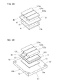
- FIG. 3B shows a 2nd joining process. It is a schematic diagram explaining the bonding area of each member. It is a perspective view of a substrate for power modules with a heat sink of a 2nd embodiment of the present invention. It is a front view of the board
- FIG. 1 It is a perspective view of a substrate for power modules with a heat sink of a 3rd embodiment of the present invention. It is a front view of the board
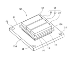
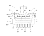
- First Embodiment 1 and 2 show a power module substrate 101 with a heat sink according to the first embodiment.
- the power module substrate 101 with a heat sink includes a power module substrate 10A and a heat sink 15A joined to the power module substrate 10A via the heat radiation side bonding material 14.
- the power module 201 is manufactured by mounting an element 91 such as a semiconductor element on the surface of a power module substrate 101 with a heat sink.
- the element 91 and the power module substrate 101 with a heat sink are resin-sealed with a molding resin 93 made of epoxy resin or the like, and the exposed surface of the power module 201 (exposed surface of the heat sink 15A) is a cooler etc. It is used in a state where it is pressed and fixed to the surface of other parts of
- the power module substrate 10 A is formed on a single ceramic substrate 11, a circuit layer 12 joined to the first surface of the ceramic substrate 11, and a second surface of the ceramic substrate 11. And a single metal layer 13 bonded.
- the ceramic substrate 11 is made of, for example, a ceramic material such as AlN (aluminum nitride), Si 3 N 4 (silicon nitride), or Al 2 O 3 (alumina).
- the circuit layer 12 is composed of a plurality of small circuit layers 21 to 23 as shown in FIG. 1 and FIG.
- the small circuit layers 21 to 23 are joined to the first surface of the ceramic substrate 11 at an interval.
- the small circuit layers 21 to 23 constituting the circuit layer 12 are a first layer 121 joined to the surface (first surface) of the ceramic substrate 11 and a surface of the first layer 121 (on the opposite side to the ceramic substrate 11). And a second layer 122 bonded to the surface).
- the first layer 121 is made of aluminum (so-called 4N aluminum) having a purity of 99.99% by mass or more, and is joined to the first surface of the ceramic substrate 11 using a brazing material.
- the second layer 122 is made of pure copper or copper alloy, and is bonded to the first layer 121 made of aluminum by solid phase diffusion bonding.
- the metal layer 13 is made of aluminum having a purity of 99.99% by mass or more, and a brazing material is used for the second surface of the ceramic substrate 11 (opposite to the circuit layer 12). Jointed.
- the heat sink 15A is bonded to the surface of the metal layer 13 (surface on the opposite side to the ceramic substrate 11) via the heat radiation side bonding material 14.
- the heat dissipating side bonding material 14 is made of copper or a copper alloy similarly to the second layer 122 of the circuit layer 12, and is bonded to the metal layer 13 and the heat sink 15A by solid phase diffusion bonding.
- the heat sink 15A is made of aluminum whose purity is lower than that of the first layer 121 of the circuit layer 12 and the metal layer 13.
- so-called 3N aluminum having a purity of 99.90 mass% or more according to JIS standard, so-called 99.0 mass% or more
- It is formed of aluminum of 2N aluminum (for example, A1050 etc.) or aluminum alloy such as A3003, A6063 and A5052.
- the heat sink 15 ⁇ / b> A has a rectangular flat top surface 51.
- the heat radiation side bonding material 14 is bonded onto the top surface 51.
- the metal layer 13 of the power module substrate 10 ⁇ / b> A is bonded to the top surface portion 51 via the heat radiation side bonding material 14.
- the upper surface of the top surface portion 51 is formed larger than the bonding surface with the heat radiation side bonding material 14.
- mounting holes 52 penetrating in the thickness direction are provided.
- the power module substrate 101 with a heat sink can be incorporated into another component by screwing or the like using the mounting holes 52 of the heat sink 15A.
- the shape of the heat sink 15A is not particularly limited, and as shown in FIGS. 1 and 2, besides a flat plate shape, a shape in which a large number of pin-shaped fins are integrally formed, and band-like fins parallel to one another are integrated. An appropriate shape such as the formed shape can be adopted.
- the thickness of the ceramic substrate 11 made of Si 3 N 4 (silicon nitride) is 0.2 mm to 1.5 mm, and the purity is 99.
- the plate thickness of the first layer 121 made of 99% by mass or more of aluminum (so-called 4N aluminum) is 0.1 mm to 2.5 mm, and the plate thickness of the metal layer 13 is 0.1 mm to 2.5 mm.
- the thickness of the second layer 122 made of oxygen free copper (C1020) is 0.1 mm to 4.0 mm, and the thickness of the heat radiation side bonding material 14 is 0.05 mm to 2.0 mm.
- the plate thickness of the top surface portion 51 of the heat sink 15A made of A6063 aluminum alloy is set to 0.5 mm to 3.0 mm. However, these dimensions are not limited to the above numerical range.
- the bonding area between the second layer 122 and the first layer 121 of the circuit layer 12 is A1 (mm 2 ), and the volume of the second layer 122 is the bonding area A1.
- the equivalent plate thickness divided by t1 (mm) the proof stress of the second layer 122 be ⁇ 1 (N / mm 2 )
- the linear expansion coefficient of the second layer 122 be ⁇ 1 (/ K).
- the joint areas A1, A2 and A3, the corresponding plate thicknesses t1, t2 and t3, the resistances ⁇ 1, ⁇ 2 and ⁇ 3, and the linear expansion coefficients ⁇ 1, ⁇ 2 and ⁇ 3 are all values at 25 ° C. (normal temperature).
- the bonding area A1 between the first layer 121 and the second layer 122 in the relational expression of the above ratio is as shown in FIG.
- the sum (a11 + a12 + a13) of the bonding areas a11 to a13 of the three first layers 121 and the three second layers 122 in the small circuit layers 21 to 23 constituting the circuit layer 12 is obtained.
- the equivalent plate thickness t1 of the second layer 122 is a value obtained by dividing the total volume V1 of the three second layers 122 in each of the small circuit layers 21 to 23 by the bonding area A1.
- the volumes of the second layers 122 of the small circuit layers 21 to 23 are v11, v12 and v13, respectively, the total volume V1 of the second layers 122 is (v11 + v12 + v13),
- the bonding area A2 between the heat dissipating side bonding material 14 and the metal layer 13 is a single area.
- the volume V2 of the material 14 is also a single volume. Accordingly, the equivalent plate thickness t2 of the heat radiation side bonding material 14 is (V2 / A2).
- areas a11 to a13 are respectively (11 mm ⁇ 36 mm) and volumes v11 to v13 are respectively (11 mm ⁇ 36 mm ⁇ 1.0 mm)
- the bonding area A2 (36 mm ⁇ 36 mm)
- the volume V2 (36 mm ⁇ 36 mm ⁇ 0.1 mm)
- the corresponding plate thickness t2 0.1 mm.
- the resistance ⁇ 3 at 25 ° C. is 50 N / mm 2 and the linear expansion coefficient ⁇ 3 is 23.4 / K.
- the equivalent plate thickness t3 of the heat sink 15A 1. It will be 9 mm.
- the element 91 according to the required function is mounted on the power module substrate 101 with a heat sink thus configured, and the power module 201 is manufactured.
- the element 91 is an electronic component provided with a semiconductor, and various semiconductor elements such as an IGBT (Insulated Gate Bipolar Transistor), a MOSFET (Metal Oxide Semiconductor Field Effect Transistor), an FWD (Free Wheeling Diode), and the like are selected.
- IGBT Insulated Gate Bipolar Transistor
- MOSFET Metal Oxide Semiconductor Field Effect Transistor
- FWD Free Wheeling Diode
- an upper electrode portion is provided at the upper portion
- a lower electrode portion is provided at the lower portion
- the lower electrode portion is joined to the upper surface of the circuit layer 12 by solder or the like.
- the element 91 is mounted on the upper surface (second layer 122) of the circuit layer 12.
- An upper electrode portion of the element 91 is connected to a circuit electrode portion or the like of the circuit layer 12 through a lead frame 92 or the like joined by solder or the like.
- the power module 201 in which the element 91 is mounted is integrated by resin-sealing the element 91 and the power module substrate 101 with a heat sink with a molding resin 93 except for the back surface side of the metal layer 13.
- a molding resin 93 for example, an epoxy resin containing a SiO 2 filler can be used, and for example, it is molded by transfer molding.
- the power module substrate 101 for a heat sink with a second layer 122 is formed on the surface of the first layer 121. It is manufactured by bonding the heat sink 15A to the surface of the heat-radiating side bonding material 14 on the surface of the metal layer 13 and the surface of the heat-radiating side bonding material 14 (second bonding step).
- a first layer aluminum plate 121a to be the first layer 121 of the circuit layer 12 is laminated on one surface of the ceramic substrate 11 via the brazing material 41, and the brazing material is also on the other surface.
- a metal layer aluminum plate 13 a to be the metal layer 13 is laminated through 41.
- Each layer is joined via the brazing material 41 by heating to a joining temperature in a vacuum atmosphere in a state where these laminated bodies are pressurized in the laminating direction, and an integrally formed joined body 30 is obtained.
- brazing material of an alloy such as an Al--Si system in the form of a foil.
- brazing material containing Mg brazing can be performed in a non-oxidizing atmosphere, not in a vacuum atmosphere.
- the conditions for brazing and bonding are, for example, a pressing force of 0.1 MPa to 1.0 MPa and a heating temperature of 630 ° C. to 650 ° C., and the pressure and heating state is maintained for 10 minutes to 50 minutes.
- the second layer copper plate 122a to be the second layer 122 is laminated on the first layer 121 of the joined body 30 obtained in the first joining step, and the heat radiation side joining material 14 is attached to the metal layer 13.
- the heat sinks 15A are stacked via the bonding plate 14a. In a state where these laminates are pressurized in the laminating direction, the first layer 121 and the second layer 122, the metal layer 13 and the heat radiation side bonding material 14, and the heat radiation side bonding material are heated by heating to the bonding temperature in a vacuum atmosphere. Solid phase diffusion bonding is performed on the heat sink 14 and the heat sink 15A.
- the pressure is 0.5 MPa to 2.0 MPa
- the heating temperature is 500 ° C. to 540 ° C.
- the pressure and heating state is maintained for 30 minutes to 120 minutes.
- the bonding surfaces of the first layer 121 and the second layer 122, the metal layer 13 and the heat radiation side bonding material 14, and the heat radiation side bonding material 14 and the heat sink 15A are smoothed by removing scratches in advance.
- the preferable heating temperature for vacuum heating in solid phase diffusion bonding is in the range of a eutectic temperature of aluminum and copper of at least -5 ° C.
- the power module substrate 101 with a heat sink configured as described above uses a copper material for the second layer 122 of the circuit layer 12, uses an aluminum material for the heat sink 15A, and uses a second layer 122 more than aluminum. It is made of copper which is excellent in conductivity.
- the heat sink 15A an aluminum material having low purity and high rigidity, that is, a high yield strength is used as the heat sink 15A, and a copper material is used as the heat radiation side joint material 14 between the metal layer 13 and the heat sink 15A.
- a relatively soft aluminum plate having a purity of 99.99% by mass or more, that is, a low proof stress is disposed on the first layer 121 and the metal layer 13 bonded to the ceramic substrate 11. Therefore, it is possible to reduce the thermal stress applied to the ceramic substrate 11 at the time of heating of the power module substrate 101 with a heat sink and the like, and to prevent the occurrence of cracking.
- the stress acting on both surfaces of the ceramic substrate 11 is unlikely to be biased when heating the power module substrate 101 with a heat sink, and the occurrence of warpage can be suppressed in the mounting process of the element 91 and the use environment.
- the bonding reliability of the power module 201 can be improved, and good heat dissipation can be exhibited.
- the power module substrate 101 with a heat sink of the present embodiment forms the top surface 51 having a larger area than the bonding surface with the heat radiation side bonding material 14 on the heat sink 15A, the power module on which the element 91 is mounted When sealing 201 with a molding resin 93 or the like, the bonding area with the molding resin 93 can be made wide. Therefore, the bonding reliability between the element 91 and the power module substrate 101 with a heat sink can be improved.
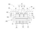
- the heat sink 15A is configured to include the flat top surface portion 51.
- the present invention also includes a configuration including a heat sink 15B in which a plurality of pin fins 53 are disposed as in the above.
- the elements common to the first embodiment are denoted by the same reference numerals to simplify the description.
- the configurations of the power module substrate 10A and the heat radiation side bonding material 14 are the same as in the first embodiment, but as shown in FIG. 5 and FIG.
- the heat sink 15 B has a shape in which a plurality of pin fins 53 are provided upright on the lower surface of the top surface portion 51.
- the entire volume V3 is a value including the top surface 51 and the pin fins 53, and from this volume V3, the equivalent plate thickness t3 of the heat sink 15B is determined.
- ⁇ 3 ⁇ is 0.70 or more and 1.30 or less.
- the ratio (A1 ⁇ t1 ⁇ ⁇ 1 ⁇ ⁇ 1) / ⁇ (A2 ⁇ t2 ⁇ ⁇ 2 ⁇ ⁇ 2) + (A3 ⁇ t3 ⁇ ⁇ 3 ⁇ ⁇ 3) ⁇ within the above-mentioned range at 25 ° C.
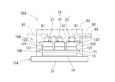
- Third Embodiment 7 and 8 show a power module substrate 103 (power module 203) with a heat sink according to the third embodiment. Also in the third embodiment, the same reference numerals are given to the elements common to the first embodiment and the second embodiment to simplify the description.
- the configurations of the substrate for power module 10A and the heat radiation side bonding material 14 are the same as in the first embodiment, but as shown in FIG. 15C has a peripheral wall 54 erected from the peripheral edge of the top surface 51 toward the circuit layer 12 side, and an accommodating recess 55 surrounded by the top surface 51 and the peripheral wall 54 is provided on the upper surface of the heat sink 15C. It is provided.
- the power module substrate 10 A and the heat sink 15 C are bonded via the heat radiation side bonding material 14. At least a portion of the heat radiation side bonding material 14 is accommodated in the accommodation recess 55 of the heat sink 15C.
- the heat dissipating side bonding material 14, the metal layer 13 and the ceramic substrate 11, and a part of the first layer 121 are housed inside the housing recess 55.
- the entire volume V3 is a value including the peripheral wall portion 54 in addition to the top surface portion 51 and the pin fins 53, and this volume V3 corresponds to the heat sink 15C.
- the plate thickness t3 is determined.
- ⁇ 3 ⁇ is 0.70 or more and 1.30 or less.
- the ratio (A1 ⁇ t1 ⁇ ⁇ 1 ⁇ ⁇ 1) / ⁇ (A2 ⁇ t2 ⁇ ⁇ 2 ⁇ ⁇ 2) + (A3 ⁇ t3 ⁇ ⁇ 3 ⁇ ⁇ 3) ⁇ at 25 ° C. is within the above range
- the symmetrical structure centering on the ceramic substrate 11 can be comprised, and generation
- the bonding area with the molding resin 93 can be made wider. Therefore, the bonding reliability between the element 91 and the power module substrate 103 with a heat sink can be improved.
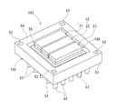
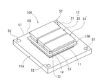
- Fourth Embodiment 9 and 10 show a power module substrate 104 (power module 204) with a heat sink according to the fourth embodiment. Also in the fourth embodiment, the same reference numerals as in the first to third embodiments described above denote the same elements in order to simplify the description.
- the configurations of the heat radiation side bonding material 14 and the heat sink 15A are the same as those of the first embodiment, but as shown in FIGS.
- the second layer 122 of the layer 12 is integrally formed with a terminal portion 123 projecting outward beyond the first layer 121.
- a lead frame 94 for external connection is connected to the terminal portion 123 by soldering or the like.
- the entire volume V1 becomes a value including the terminal portion 123, and the equivalent plate thickness t1 of the second layer 122 can be determined from the volume V1. .
- ⁇ 3) ⁇ is 0.70 or more and 1.30 or less.
- the ratio (A1 ⁇ t1 ⁇ ⁇ 1 ⁇ ⁇ 1) / ⁇ (A2 ⁇ t2 ⁇ ⁇ 2 ⁇ ⁇ 2) + (A3 ⁇ t3 ⁇ ⁇ 3 ⁇ ⁇ 3) ⁇ at 25 ° C. falls within the above range
- the symmetrical structure centering on the ceramic substrate 11 can be comprised, and generation
- the substrate 104 for a power module with a heat sink in which the shapes of the circuit layer 12 and the heat sink 15A are formed by various variations, not only the rigidity of each member but also the equivalent plate obtained by dividing the volume of each member by the bonding area
- the symmetrical structure centering on the ceramic substrate 11 can be comprised, and generation
- the members constituting the samples of Inventive Examples 1 to 10 and Comparative Examples 1 to 3 include a ceramic substrate made of AlN having a thickness of 0.635 mm, a first layer made of 4N-Al having a thickness of 0.6 mm, and a metal layer. And prepared.
- the heat dissipating side bonding material and the heat sink the respective materials, equivalent plate thickness, bonding area, linear expansion coefficient (CTE) and proof stress are shown in Tables 1 to 3.
- the “embodiments” in Tables 1 and 2 show in which embodiment form (shape) the second layer and the heat sink of each sample are formed.
- the “ratio” in Table 4 indicates the ratio (A1 ⁇ t1 ⁇ ⁇ 1 ⁇ ⁇ 1) / ⁇ (A2 ⁇ t2 ⁇ ⁇ 2 ⁇ ⁇ 2) + (A3 ⁇ t3 ⁇ ⁇ 3 ⁇ ⁇ 3) ⁇ at 25 ° C.
- the “yield strength” in FIGS. 1 to 3 was measured at 25 ° C. by a method based on JIS G0567: 2012.
- the amount of warpage was measured with a moiré-type three-dimensional shape measuring machine for the change in flatness at the central portion (in the range of 40 mm ⁇ 40 mm) of the back of the heat sink.
- the difference between the initial warpage and the warpage during heating was 150 ⁇ m or less, the warpage amount was small, the evaluation was good “A”, and when the difference exceeded 150 ⁇ m, the warpage amount was evaluated as “B”.
- Table 4 shows the results.
Landscapes
- Engineering & Computer Science (AREA)
- Chemical & Material Sciences (AREA)
- Physics & Mathematics (AREA)
- General Physics & Mathematics (AREA)
- Condensed Matter Physics & Semiconductors (AREA)
- Computer Hardware Design (AREA)
- Microelectronics & Electronic Packaging (AREA)
- Power Engineering (AREA)
- Materials Engineering (AREA)
- Ceramic Engineering (AREA)
- Geometry (AREA)
- Structural Engineering (AREA)
- Organic Chemistry (AREA)
- Cooling Or The Like Of Semiconductors Or Solid State Devices (AREA)
Priority Applications (4)
| Application Number | Priority Date | Filing Date | Title |
|---|---|---|---|
| KR1020207020962A KR102387210B1 (ko) | 2018-01-24 | 2019-01-23 | 히트 싱크 부착 파워 모듈용 기판 및 파워 모듈 |
| CN201980007458.0A CN111602238B (zh) | 2018-01-24 | 2019-01-23 | 带散热片的功率模块用基板及功率模块 |
| US16/963,667 US11355415B2 (en) | 2018-01-24 | 2019-01-23 | Heat sink-attached power module substrate board and power module |
| EP19743122.4A EP3745453B1 (en) | 2018-01-24 | 2019-01-23 | Substrate for power module with heat sink, and power module |
Applications Claiming Priority (2)
| Application Number | Priority Date | Filing Date | Title |
|---|---|---|---|
| JP2018-009313 | 2018-01-24 | ||
| JP2018009313A JP6601512B2 (ja) | 2018-01-24 | 2018-01-24 | ヒートシンク付きパワーモジュール用基板及びパワーモジュール |
Publications (1)
| Publication Number | Publication Date |
|---|---|
| WO2019146640A1 true WO2019146640A1 (ja) | 2019-08-01 |
Family
ID=67395646
Family Applications (1)
| Application Number | Title | Priority Date | Filing Date |
|---|---|---|---|
| PCT/JP2019/002076 Ceased WO2019146640A1 (ja) | 2018-01-24 | 2019-01-23 | ヒートシンク付きパワーモジュール用基板及びパワーモジュール |
Country Status (7)
| Country | Link |
|---|---|
| US (1) | US11355415B2 (enExample) |
| EP (1) | EP3745453B1 (enExample) |
| JP (1) | JP6601512B2 (enExample) |
| KR (1) | KR102387210B1 (enExample) |
| CN (1) | CN111602238B (enExample) |
| TW (1) | TWI758579B (enExample) |
| WO (1) | WO2019146640A1 (enExample) |
Cited By (2)
| Publication number | Priority date | Publication date | Assignee | Title |
|---|---|---|---|---|
| WO2023032462A1 (ja) * | 2021-09-02 | 2023-03-09 | ローム株式会社 | 半導体装置およびその製造方法 |
| WO2025027845A1 (ja) * | 2023-08-03 | 2025-02-06 | 三菱電機株式会社 | 半導体装置および半導体装置の製造方法 |
Families Citing this family (6)
| Publication number | Priority date | Publication date | Assignee | Title |
|---|---|---|---|---|
| JP2021061341A (ja) * | 2019-10-08 | 2021-04-15 | 昭和電工株式会社 | 半導体冷却装置 |
| JP7487533B2 (ja) | 2020-04-02 | 2024-05-21 | 富士電機株式会社 | 半導体モジュールおよび車両 |
| DE102021212232A1 (de) * | 2021-10-29 | 2023-05-04 | Zf Friedrichshafen Ag | Leistungsmodul und verfahren zum montieren eines leistungsmoduls |
| DE102022207525A1 (de) | 2022-07-22 | 2024-01-25 | Vitesco Technologies Germany Gmbh | Leistungsmodul und Verfahren zur Herstellung desselben, Stromrichter mit einem Leistungsmodul |
| TWI811136B (zh) * | 2022-10-17 | 2023-08-01 | 創世電股份有限公司 | 半導體功率元件 |
| TWI836729B (zh) * | 2022-11-16 | 2024-03-21 | 財團法人工業技術研究院 | 陶瓷電路板結構及功率模組 |
Citations (8)
| Publication number | Priority date | Publication date | Assignee | Title |
|---|---|---|---|---|
| JP2003078086A (ja) * | 2001-09-04 | 2003-03-14 | Kubota Corp | 半導体素子モジュール基板の積層構造 |
| JP2015211125A (ja) * | 2014-04-25 | 2015-11-24 | 三菱マテリアル株式会社 | パワーモジュール用基板及びヒートシンク付パワーモジュール用基板並びにヒートシンク付パワーモジュール |
| JP2015216370A (ja) | 2014-04-25 | 2015-12-03 | 三菱マテリアル株式会社 | ヒートシンク付きパワーモジュール用基板及びパワーモジュール |
| JP2016027645A (ja) * | 2014-07-04 | 2016-02-18 | 三菱マテリアル株式会社 | 放熱板付パワーモジュール用基板及びパワーモジュール |
| JP2016046356A (ja) * | 2014-08-21 | 2016-04-04 | 三菱マテリアル株式会社 | 放熱板付パワーモジュール用基板及びパワーモジュール |
| JP2016181549A (ja) * | 2015-03-23 | 2016-10-13 | 三菱マテリアル株式会社 | ヒートシンク付きパワーモジュール用基板 |
| JP2017073483A (ja) | 2015-10-08 | 2017-04-13 | 三菱マテリアル株式会社 | ヒートシンク付きパワーモジュール用基板及びパワーモジュール |
| JP2018009313A (ja) | 2016-07-12 | 2018-01-18 | 鹿島建設株式会社 | 地盤改良工法及びプレキャスト地盤の製造方法 |
Family Cites Families (6)
| Publication number | Priority date | Publication date | Assignee | Title |
|---|---|---|---|---|
| JP5403129B2 (ja) | 2012-03-30 | 2014-01-29 | 三菱マテリアル株式会社 | パワーモジュール用基板、ヒートシンク付パワーモジュール用基板、パワーモジュール、及びパワーモジュール用基板の製造方法 |
| WO2014142310A1 (ja) * | 2013-03-14 | 2014-09-18 | 三菱マテリアル株式会社 | 接合体、パワーモジュール用基板、及びヒートシンク付パワーモジュール用基板 |
| JP6621076B2 (ja) * | 2013-03-29 | 2019-12-18 | 三菱マテリアル株式会社 | パワーモジュール用基板、ヒートシンク付パワーモジュール用基板及びパワーモジュール |
| KR102232098B1 (ko) * | 2013-10-10 | 2021-03-24 | 미쓰비시 마테리알 가부시키가이샤 | 히트 싱크가 부착된 파워 모듈용 기판 및 그 제조 방법 |
| EP3166140B1 (en) * | 2014-07-04 | 2020-06-03 | Mitsubishi Materials Corporation | Substrate unit for power modules, and power module |
| JP6638284B2 (ja) * | 2015-09-28 | 2020-01-29 | 三菱マテリアル株式会社 | 放熱板付パワーモジュール用基板及びパワーモジュール |
-
2018
- 2018-01-24 JP JP2018009313A patent/JP6601512B2/ja active Active
-
2019
- 2019-01-23 EP EP19743122.4A patent/EP3745453B1/en active Active
- 2019-01-23 KR KR1020207020962A patent/KR102387210B1/ko active Active
- 2019-01-23 CN CN201980007458.0A patent/CN111602238B/zh active Active
- 2019-01-23 WO PCT/JP2019/002076 patent/WO2019146640A1/ja not_active Ceased
- 2019-01-23 US US16/963,667 patent/US11355415B2/en active Active
- 2019-01-24 TW TW108102677A patent/TWI758579B/zh active
Patent Citations (8)
| Publication number | Priority date | Publication date | Assignee | Title |
|---|---|---|---|---|
| JP2003078086A (ja) * | 2001-09-04 | 2003-03-14 | Kubota Corp | 半導体素子モジュール基板の積層構造 |
| JP2015211125A (ja) * | 2014-04-25 | 2015-11-24 | 三菱マテリアル株式会社 | パワーモジュール用基板及びヒートシンク付パワーモジュール用基板並びにヒートシンク付パワーモジュール |
| JP2015216370A (ja) | 2014-04-25 | 2015-12-03 | 三菱マテリアル株式会社 | ヒートシンク付きパワーモジュール用基板及びパワーモジュール |
| JP2016027645A (ja) * | 2014-07-04 | 2016-02-18 | 三菱マテリアル株式会社 | 放熱板付パワーモジュール用基板及びパワーモジュール |
| JP2016046356A (ja) * | 2014-08-21 | 2016-04-04 | 三菱マテリアル株式会社 | 放熱板付パワーモジュール用基板及びパワーモジュール |
| JP2016181549A (ja) * | 2015-03-23 | 2016-10-13 | 三菱マテリアル株式会社 | ヒートシンク付きパワーモジュール用基板 |
| JP2017073483A (ja) | 2015-10-08 | 2017-04-13 | 三菱マテリアル株式会社 | ヒートシンク付きパワーモジュール用基板及びパワーモジュール |
| JP2018009313A (ja) | 2016-07-12 | 2018-01-18 | 鹿島建設株式会社 | 地盤改良工法及びプレキャスト地盤の製造方法 |
Cited By (2)
| Publication number | Priority date | Publication date | Assignee | Title |
|---|---|---|---|---|
| WO2023032462A1 (ja) * | 2021-09-02 | 2023-03-09 | ローム株式会社 | 半導体装置およびその製造方法 |
| WO2025027845A1 (ja) * | 2023-08-03 | 2025-02-06 | 三菱電機株式会社 | 半導体装置および半導体装置の製造方法 |
Also Published As
| Publication number | Publication date |
|---|---|
| CN111602238B (zh) | 2023-11-10 |
| TW201933560A (zh) | 2019-08-16 |
| JP2019129208A (ja) | 2019-08-01 |
| US20210074607A1 (en) | 2021-03-11 |
| KR20200112845A (ko) | 2020-10-05 |
| JP6601512B2 (ja) | 2019-11-06 |
| US11355415B2 (en) | 2022-06-07 |
| EP3745453A1 (en) | 2020-12-02 |
| CN111602238A (zh) | 2020-08-28 |
| TWI758579B (zh) | 2022-03-21 |
| KR102387210B1 (ko) | 2022-04-14 |
| EP3745453A4 (en) | 2021-10-27 |
| EP3745453B1 (en) | 2022-09-21 |
Similar Documents
| Publication | Publication Date | Title |
|---|---|---|
| JP6488917B2 (ja) | 放熱板付パワーモジュール用基板及びパワーモジュール | |
| TWI758579B (zh) | 附散熱座功率模組用基板及功率模組 | |
| CN100578768C (zh) | 散热装置及功率模块 | |
| JP6435945B2 (ja) | ヒートシンク付きパワーモジュール用基板 | |
| EP3166140B1 (en) | Substrate unit for power modules, and power module | |
| JP7151583B2 (ja) | ヒートシンク付き絶縁回路基板 | |
| CN104603933A (zh) | 功率模块用基板及功率模块 | |
| CN110998839B (zh) | 功率模块 | |
| JP6417834B2 (ja) | 冷却器付パワーモジュール用基板及び冷却器付パワーモジュール用基板の製造方法 | |
| JP6435711B2 (ja) | 放熱板付パワーモジュール用基板及びパワーモジュール | |
| JP2019129208A5 (enExample) | ||
| JP2005011922A (ja) | ヒートシンクを備えた両面銅貼り基板、およびこれを用いた半導体装置 | |
| JP7163583B2 (ja) | 半導体装置 | |
| JP6681660B2 (ja) | ヒートシンク付パワーモジュール用基板及びパワーモジュール | |
| JP6565735B2 (ja) | パワーモジュール用基板及びパワーモジュール並びにパワーモジュール用基板の製造方法 | |
| CN111819681B (zh) | 带散热器的绝缘电路基板 | |
| JP2004343035A (ja) | 放熱部品、回路基板および半導体装置 | |
| JP7063559B2 (ja) | ベース板及びパワーモジュール | |
| WO2025046903A1 (ja) | 半導体装置および半導体装置の製造方法 |
Legal Events
| Date | Code | Title | Description |
|---|---|---|---|
| 121 | Ep: the epo has been informed by wipo that ep was designated in this application |
Ref document number: 19743122 Country of ref document: EP Kind code of ref document: A1 |
|
| NENP | Non-entry into the national phase |
Ref country code: DE |
|
| ENP | Entry into the national phase |
Ref document number: 2019743122 Country of ref document: EP Effective date: 20200824 |