WO2019139150A1 - 光学積層体、偏光板、ディスプレイパネル及び画像表示装置 - Google Patents
光学積層体、偏光板、ディスプレイパネル及び画像表示装置 Download PDFInfo
- Publication number
- WO2019139150A1 WO2019139150A1 PCT/JP2019/000793 JP2019000793W WO2019139150A1 WO 2019139150 A1 WO2019139150 A1 WO 2019139150A1 JP 2019000793 W JP2019000793 W JP 2019000793W WO 2019139150 A1 WO2019139150 A1 WO 2019139150A1
- Authority
- WO
- WIPO (PCT)
- Prior art keywords
- refractive index
- low refractive
- index layer
- optical laminate
- fine particles
- Prior art date
Links
Images


Classifications
-
- G—PHYSICS
- G02—OPTICS
- G02B—OPTICAL ELEMENTS, SYSTEMS OR APPARATUS
- G02B5/00—Optical elements other than lenses
- G02B5/30—Polarising elements
- G02B5/3025—Polarisers, i.e. arrangements capable of producing a definite output polarisation state from an unpolarised input state
- G02B5/3033—Polarisers, i.e. arrangements capable of producing a definite output polarisation state from an unpolarised input state in the form of a thin sheet or foil, e.g. Polaroid
-
- B—PERFORMING OPERATIONS; TRANSPORTING
- B32—LAYERED PRODUCTS
- B32B—LAYERED PRODUCTS, i.e. PRODUCTS BUILT-UP OF STRATA OF FLAT OR NON-FLAT, e.g. CELLULAR OR HONEYCOMB, FORM
- B32B7/00—Layered products characterised by the relation between layers; Layered products characterised by the relative orientation of features between layers, or by the relative values of a measurable parameter between layers, i.e. products comprising layers having different physical, chemical or physicochemical properties; Layered products characterised by the interconnection of layers
- B32B7/02—Physical, chemical or physicochemical properties
- B32B7/023—Optical properties
-
- G—PHYSICS
- G02—OPTICS
- G02B—OPTICAL ELEMENTS, SYSTEMS OR APPARATUS
- G02B1/00—Optical elements characterised by the material of which they are made; Optical coatings for optical elements
- G02B1/10—Optical coatings produced by application to, or surface treatment of, optical elements
- G02B1/11—Anti-reflection coatings
-
- G—PHYSICS
- G02—OPTICS
- G02B—OPTICAL ELEMENTS, SYSTEMS OR APPARATUS
- G02B1/00—Optical elements characterised by the material of which they are made; Optical coatings for optical elements
- G02B1/10—Optical coatings produced by application to, or surface treatment of, optical elements
- G02B1/14—Protective coatings, e.g. hard coatings
-
- G—PHYSICS
- G02—OPTICS
- G02B—OPTICAL ELEMENTS, SYSTEMS OR APPARATUS
- G02B5/00—Optical elements other than lenses
- G02B5/02—Diffusing elements; Afocal elements
-
- G—PHYSICS
- G02—OPTICS
- G02B—OPTICAL ELEMENTS, SYSTEMS OR APPARATUS
- G02B5/00—Optical elements other than lenses
- G02B5/30—Polarising elements
-
- G—PHYSICS
- G02—OPTICS
- G02F—OPTICAL DEVICES OR ARRANGEMENTS FOR THE CONTROL OF LIGHT BY MODIFICATION OF THE OPTICAL PROPERTIES OF THE MEDIA OF THE ELEMENTS INVOLVED THEREIN; NON-LINEAR OPTICS; FREQUENCY-CHANGING OF LIGHT; OPTICAL LOGIC ELEMENTS; OPTICAL ANALOGUE/DIGITAL CONVERTERS
- G02F1/00—Devices or arrangements for the control of the intensity, colour, phase, polarisation or direction of light arriving from an independent light source, e.g. switching, gating or modulating; Non-linear optics
- G02F1/01—Devices or arrangements for the control of the intensity, colour, phase, polarisation or direction of light arriving from an independent light source, e.g. switching, gating or modulating; Non-linear optics for the control of the intensity, phase, polarisation or colour
- G02F1/13—Devices or arrangements for the control of the intensity, colour, phase, polarisation or direction of light arriving from an independent light source, e.g. switching, gating or modulating; Non-linear optics for the control of the intensity, phase, polarisation or colour based on liquid crystals, e.g. single liquid crystal display cells
- G02F1/133—Constructional arrangements; Operation of liquid crystal cells; Circuit arrangements
- G02F1/1333—Constructional arrangements; Manufacturing methods
- G02F1/1335—Structural association of cells with optical devices, e.g. polarisers or reflectors
- G02F1/133502—Antiglare, refractive index matching layers
-
- H—ELECTRICITY
- H10—SEMICONDUCTOR DEVICES; ELECTRIC SOLID-STATE DEVICES NOT OTHERWISE PROVIDED FOR
- H10K—ORGANIC ELECTRIC SOLID-STATE DEVICES
- H10K59/00—Integrated devices, or assemblies of multiple devices, comprising at least one organic light-emitting element covered by group H10K50/00
- H10K59/50—OLEDs integrated with light modulating elements, e.g. with electrochromic elements, photochromic elements or liquid crystal elements
Definitions
- the present invention relates to an optical laminate, a polarizing plate, a display panel, and an image display device.
- An image display surface in an image display apparatus such as a liquid crystal display (LCD), a cathode ray tube display (CRT), a plasma display (PDP), an electroluminescence display (ELD), a field emission display (FED),
- LCD liquid crystal display
- CRT cathode ray tube display
- PDP plasma display
- ELD electroluminescence display
- FED field emission display
- an antiglare film having irregularities on the surface and an antireflective optical laminate having an antireflective layer on the surface are provided.
- Such an optical laminate for preventing reflection suppresses the reflection of an image or reduces the reflectance by light scattering or interference.
- the optical laminates for preventing reflection there is known one in which an antiglare layer having a concavo-convex shape is formed on the surface of a transparent substrate and a low refractive index layer having a low refractive index is provided thereon.
- Such an optical laminate is packed in a packaging material and transported or transported, but since the convex portion is mainly present on the surface of the low refractive index layer of the uneven shape of the antiglare layer, the optical laminate and the packaging are packaged. It was thought that the surface of the low refractive index layer was hard to be scratched when it was in point contact when it was in contact with the material. However, in practice, rubbing between the optical laminate and the packaging material causes a problem such as scratching. Therefore, there is a strong demand for improving the abrasion resistance of the optical laminate.
- a compound having a polymerizable unsaturated group is used in the antiglare layer to impart hardness to the antiglare layer, or inorganic particles are contained in the low refractive index layer to form the low refractive index layer.
- a method of improving the scratch resistance of an optical laminate by imparting hardness or the like is disclosed (see, for example, Patent Document 1).
- An object of the present invention is to provide an optical laminate having excellent scratch resistance while having anti-reflection performance in view of the above-mentioned current situation.
- the present invention is an optical laminate in which an antiglare layer and a low refractive index layer are laminated in this order on one surface of a light transmitting substrate, and any 5 ⁇ m square of the surface of the low refractive index layer
- the optical laminate is characterized in that when the arithmetic average roughness Ra of the unevenness in the region and the ten-point average roughness Rz of the unevenness are measured, the Ra is 4 nm or less and the Rz is 60 nm or less
- the first present invention it is also referred to as the first present invention.
- the present invention is an optical laminate in which an antiglare layer and a low refractive index layer are laminated in this order on one surface of a light transmitting substrate, any surface of the low refractive index layer
- the above Ra is 1.5 nm or less
- the above Rz is 30 nm or less
- the optical laminate is also characterized in that the hardness when the pressed indenter is indented by 300 nm is higher than the hardness when the indenter measured by the nanoindentation method is depressed by 30 nm (hereinafter also referred to as second invention) ).
- the optical layered body of the first present invention and the optical layered body of the second present invention are not distinguished, they will be referred to as “the optical layered body of the present invention”.
- the hardness of the surface of the low refractive index layer measured by the nano-indentation method under the condition of an indentation depth of 30 nm is preferably 440 MPa or more.
- the low refractive index layer preferably contains hollow silica fine particles.
- the present invention is also a polarizing plate comprising a polarizing element, which is characterized in that the optical laminate of the present invention is provided on the surface of the polarizing element.
- the present invention is also a display panel comprising the optical laminate of the present invention or the polarizing plate of the present invention.
- the present invention is also an image display device comprising the optical laminate of the present invention or the polarizing plate of the present invention.
- the present inventors found that the low refractive index located on the surface Method for imparting hardness to a refractive index layer, method for imparting flatness to the low refractive index layer, method for imparting slipperiness to the surface of the low refractive index layer, and the low refractive index layer and the antiglare layer It has been found that the method of imparting interlayer adhesion can improve the scratch resistance of an optical laminate.
- the inventors of the present invention observed in detail the flaws generated on the surface of the optical laminate having the conventional antiglare layer and the low refractive index layer, and it was found that the flaws were generated regardless of the uneven shape. I found it. That is, there are two scratch modes, and one is a reduction in film thickness due to scraping of the low refractive index layer, and an interference color caused by interference of reflected light from each layer of the optical laminate having the low refractive index layer. The other was that the low refractive index layers were all scraped off and scratched.
- the optical laminate of the present invention at least an antiglare layer and a low refractive index layer are formed in this order on a light transmitting substrate.
- the low refractive index layer is a layer having a refractive index lower than the refractive index of components other than the low refractive index layer, such as a light transmitting substrate and an antiglare layer constituting the optical laminate of the present invention.
- Means The arithmetic mean roughness Ra of the surface of the low refractive index layer described later, the ten-point mean roughness Rz of asperities, and the hardness measured by the nanoindentation method are on one surface of the light transmitting substrate.
- At least an antiglare layer and a low refractive index layer were measured in this order on the optical laminate.
- the layer configuration of the optical laminate can be preferably cross-sectionally observed at a magnification of 1000 to 20,000 times by using an STEM.
- Rz is an index of the height of irregularities on the surface of the low refractive index layer.
- Ra and Rz are used to judge the texture and flatness of the surface of the low refractive index layer, but Ra is a parameter whose actual shape is unknown, but the target is low.
- the average height of the whole of various micro shapes of texture present on the refractive index layer surface can be known, and the height of the entire texture can be controlled.
- Rz is an average value of the highest place and the lowest place among textures of the low refractive index layer surface. Since the texture of the surface of the low refractive index layer is only an averaged result if it is only Ra, there is a possibility that discrimination can not be made even if there are sudden high convex portions or low concave portions. Since the irregularities cause scratches, there is insufficient control of the texture of the surface of the low refractive index layer. Therefore, in the present invention, the maximum allowable height and the maximum allowable depth are controlled by Rz in addition to the above-mentioned Ra, and as a result, the control of the above-mentioned sudden convex portion or concave portion becomes possible.
- the low refractive index layer is extremely excellent in flatness, and specifically, JIS B0601 (in any arbitrary 5 ⁇ m square area of the surface of the low refractive index layer)
- the above-mentioned Ra is 4 nm or less
- the above-mentioned Rz is 60 nm or less when the arithmetic mean roughness Ra of the irregularities defined in 2001) and the ten-point average roughness Rz of the irregularities are measured.
- the flatness of the optical layered body of the present invention is insufficient and the scratch resistance becomes insufficient.
- the optical layered body according to the first aspect of the present invention at least the antiglare layer and the low refractive index layer are formed in this order on the light transmitting substrate, and therefore, on the surface of the low refractive index layer.
- the concavo-convex shape derived from the above antiglare layer is formed, and the antiglare performance is ensured, but the surface of the above low refractive index layer is extremely flattened when viewed in a microscopic field of view (5 ⁇ m square area) It is. Therefore, the optical laminate of the first present invention has excellent scratch resistance.
- the arithmetic mean roughness (Ra) of the surface of the low refractive index layer in a microscopic field of view is more preferably 3 nm or less, and still more preferably 2 nm or less.
- the ten-point average roughness (Rz) of the surface of the low refractive index layer in a microscopic field of view is more preferably 45 nm or less, and still more preferably 35 nm or less.
- the above-mentioned excellent scuff resistance means, for example, that no scuffing occurs in a scuffing test in which a friction load of 700 g / cm 2 using a steel wool of Bonstar No. 0000 made of Bonstar U.S.A.
- the above scanning range of 5 ⁇ m is to determine and control the texture state and flatness of the surface of the low refractive index layer that is originally laminated on the surface of the antiglare layer with some irregularities.
- the visual field area to be measured is as narrow as possible. If the visual field area is larger than the above range, the measurement itself with AFM may become difficult including defects such as deflection of the measurement sample, unevenness of the antiglare layer, and environmental foreign matter. On the other hand, when the visual field area is narrower than the above range, the surface roughness of the low refractive index layer may not be evaluated properly.
- Measurement samples are prepared in the order of (1) to (4) below.
- the sample is prepared by cutting into 8 mm ⁇ 8 mm size smaller than the carbon tape.
- a carbon tape is attached to the back surface of the sample to prepare a measurement sample.
- Arithmetic mean roughness Ra extracts only the reference length (l) in the direction of the mean line from the roughness curve of the surface of the obtained measurement sample according to JIS B 0031 (1994), and the direction of the mean line of this removed portion
- X be the X axis
- Y be the direction of longitudinal magnification
- the value obtained by the following equation is expressed in micrometers ( ⁇ m) .
- the ten-point average roughness Rz extracts only the reference length (l) in the direction of the mean line from the roughness curve of the surface of the obtained measurement sample, and Average value of the absolute value of the highest peak to the fifth peak (Yp) measured in the direction of longitudinal magnification and average value of the absolute value of the lowest peak to the fifth bottom (Yv) (Yv) The sum of and is obtained as the following equation, and this value is expressed in micrometers ( ⁇ m).
- the above Yp 1 , Yp 2 , Yp 3 , Yp 4 , and Yp 5 are the elevations of the fifth to the fifth highest peaks of the extraction portion with respect to the reference length l.
- the above Yv 1 , Yv 2 , Yv 3 , Yv 4 and Yv 5 are the elevations of the valley bottoms from the lowest valley bottom to the fifth valley bottom with respect to the reference length l.
- the low refractive index layer in the optical laminate according to the first aspect of the present invention preferably has a hardness of 440 MPa or more on the surface of the low refractive index layer measured under the condition of 30 nm indentation depth by nanoindentation method.
- the nanoindentation method is a physical quantity that can be measured directly, and is a method that can determine hardness and elastic modulus using load, displacement of the indenter from the place where the indenter comes in contact with the sample surface, and time. is there. That is, as shown in FIG.
- the surface at the time of plastic deformation is treated as the starting point of analysis. That is, as shown in FIG. 1 (b), in the press-fit load-press-fit depth curve, the hardness is determined focusing on the unloading curve which is a simple elastic recovery. Therefore, the hardness of the nanoindentation method is a hardness at which mainly the property of elastic deformation appears in the cured resin layer made of the polymer material as in the present invention.
- the force which repels the surface of the layer to be scratched immediately after the layer itself receives some rubbing force.
- the mechanism is evaluated by the hardness by the nanoindentation method among various indentation hardness test methods because it matches with the mechanism of the hardness by the nanoindentation method described above (force to recover elastically after plastic deformation).
- We selected as optimal for the present invention.
- abrasion resistance of about 300 g / cm 2 to 500 g / cm 2 can be obtained, and it is preferably used for a home-fixed TV monitor display.
- displays in recent years are widely used for digital signage at stations and airports, etc.
- abrasion resistance such as a load of 600 g / cm 2 or more may be preferred. In that case, it was found that it is effective to improve the hardness involved in the elastic deformation and elastic recovery force of the low refractive index layer itself which is the surface layer which receives the rubbing force as well as the flatness.
- the reason why the indentation depth is 30 nm is to determine the hardness to which the elastic deformation force of the low refractive index layer itself is involved. In addition, a stable measurement is possible at this depth, and the influence of the underlying layer, for example, the antiglare layer, is scarce.
- the hardness of the surface of the low refractive index layer measured under the conditions of an indentation depth of 30 nm by the nanoindentation method is more preferably 500 MPa or more, and still more preferably 600 MPa or more.
- the upper limit of the hardness of the low refractive index layer surface measured under the condition of the indentation depth of 30 nm is preferably 4000 MPa, more preferably 2000 MPa, and still more preferably 1600 MPa.
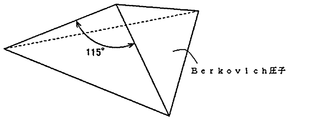
- the hardness by the nanoindentation method is measured in a displacement amount control mode using “TI950 TriboIndenter” manufactured by HYSITRON (Hiditron). Specifically, in the low refractive index layer, a Berkovich indenter (triangular pyramid, made of diamond, 115 ° in inclination angle) as shown in FIG.
- the indentation depth of the indenter selects 30 nm which can stably measure the hardness by nanoindentation method, and the hardness measurement by nanoindentation method is 25 ° C ⁇ 5 ° C, relative humidity 30% or more and 70% or less Shall be conducted under the following circumstances.
- the following method can be used as a method for producing a measurement sample of the nanoindentation method.
- An adhesive resin product name "Aron Alpha (registered trademark) for general use, manufactured by Toa Gosei Co., Ltd.
- the above adhesive resin is dropped on the central portion of the slide glass 1 (product name “slide glass (cut-off type) 1-9645-11”, manufactured by As One Corporation). At this time, the adhesive resin is not spread, and the dropping is one drop so that the adhesive resin does not protrude from the optical laminate when it is spread as described later.
- the optical laminate cut into the above size is brought into contact with the slide glass so that the low refractive index layer side is the upper surface and the adhesive resin is positioned at the center of the optical laminate, the slide glass 1 and the optical laminate Push and spread the adhesive resin between them and temporarily bond.
- another new slide glass 2 is placed on the optical laminate to obtain a laminate of slite glass 1 / adhesive resin / optical laminate / slide glass 2.
- a weight of 30 g or more and 50 g or less is placed on the slide glass 2, and in this state, it is left at room temperature for 12 hours. Thereafter, the weight and the slide glass 2 are removed and used as a measurement sample.
- the four corners of the optical laminate fixed with the adhesive resin may be further fixed with a tape (product name “Cellotape (registered trademark)”, manufactured by Nichiban Co., Ltd.).
- the following method can be used, for example.
- the above-mentioned measurement sample is fixed to the measurement stage of the measuring instrument installed parallel to the vibration isolation table.
- a method of fixing the four sides of the slide glass 1 with a tape product name "Sellotape (registered trademark), manufactured by Nichiban Co., Ltd.) or the like is optional, and the sample for measurement may not move.
- the said measuring instrument has an air suction system, you may fix by an air suction system.
- the indentation hardness at the position of 30 nm indentation amount on the surface of the low refractive index layer is measured under the following measurement conditions.
- the indentation hardness is an arithmetic mean value of the hardness of the obtained five points by measuring arbitrary five points in the vicinity of the surface center (region where the adhesive resin exists) of the low refractive index layer of the measurement sample.
- the low refractive index layer is observed at a magnification of 50 times to 500 times using a microscope, and a portion having an extremely convex structure and a portion having an extremely concave structure And should be selected from parts that are as flat as possible.
- the following conditions are preferably used as the specific measurement conditions of the hardness when the indenter is indented by 30 nm.
- Used indenter Berkovich indenter (triangular pyramid)
- Measurement conditions Displacement control method Displacement control mode
- Maximum displacement 30 nm Arrival time to maximum displacement: Holding time at 3 seconds maximum displacement: 5 seconds
- Test score 5 points (this arithmetic mean value is taken as the measurement result)
- the low refractive index layer is extremely excellent in flatness, and specifically, it is JIS in an arbitrary 5 ⁇ m square area of the surface of the low refractive index layer.
- the Ra is 1.5 nm or less
- the Rz is 30 nm or less. That is, in the optical laminate of the second invention, at least the antiglare layer and the low refractive index layer are formed in this order on the light transmitting substrate, and therefore, on the surface of the low refractive index layer.
- the concavo-convex shape derived from the above antiglare layer is formed, and the antiglare performance is ensured, but the surface of the above low refractive index layer is extremely flattened when viewed in a microscopic field of view (5 ⁇ m square area) It is.
- the range of such arithmetic average roughness (Ra) and ten-point average roughness (Rz) is satisfied, and further, the surface of the low refractive index layer is measured by nano-indentation method
- the arithmetic average roughness (Ra) of the surface of the low refractive index layer is preferably 1.2 nm or less, more preferably 1.0 nm or less.
- the ten-point average roughness (Rz) of the surface of the low refractive index layer is preferably 25 nm or less, more preferably 20 nm or less.
- the above-mentioned excellent scuff resistance means, for example, that no scuffing occurs in a scuffing test in which a friction load of 700 g / cm 2 using a steel wool of Bonstar No. 0000 made of Bonstar U.S.A.
- the selection in the solvent of the composition for the low refractive index layer described later, the low refractive index described later can be suitably formed depending on the drying conditions and curing conditions when applying the composition for layer to form a coating, selection of the leveling agent contained in the composition for antiglare layer described later, and the like.
- the arithmetic mean roughness (Ra) and the ten-point mean roughness (Rz) of the surface of the low refractive index layer in the optical laminate according to the second invention are AFM: SPM-9600 (Shimadzu).
- the above scanning range of 5 ⁇ m is to determine and control the texture state and flatness of the surface of the low refractive index layer that is originally laminated on the surface of the antiglare layer with some irregularities.
- the visual field area to be measured is as narrow as possible. If the visual field area is larger than the above range, the measurement itself with AFM may become difficult including defects such as deflection of the measurement sample, unevenness of the antiglare layer, and environmental foreign matter. On the other hand, when the visual field area is narrower than the above range, the surface roughness of the low refractive index layer may not be evaluated properly.
- Measurement samples are prepared in the order of (1) to (4) below.
- the sample is prepared by cutting into 8 mm ⁇ 8 mm size smaller than the carbon tape.
- a carbon tape is attached to the back surface of the sample to prepare a measurement sample.
- Arithmetic mean roughness Ra extracts only the reference length (l) in the direction of the mean line from the roughness curve of the surface of the obtained measurement sample according to JIS B 0031 (1994), and the direction of the mean line of this removed portion
- X be the X axis
- Y be the direction of longitudinal magnification
- the value obtained by the following equation is expressed in micrometers ( ⁇ m) .
- the ten-point average roughness Rz extracts only the reference length (l) in the direction of the mean line from the roughness curve of the surface of the obtained measurement sample, and Average value of the absolute value of the highest peak to the fifth peak (Yp) measured in the direction of longitudinal magnification and average value of the absolute value of the lowest peak to the fifth bottom (Yv) (Yv) The sum of and is obtained as the following equation, and this value is expressed in micrometers ( ⁇ m).
- the above Yp 1 , Yp 2 , Yp 3 , Yp 4 , and Yp 5 are the elevations of the fifth to the fifth highest peaks of the extraction portion with respect to the reference length l.
- the above Yv 1 , Yv 2 , Yv 3 , Yv 4 and Yv 5 are the elevations of the valley bottoms from the lowest valley bottom to the fifth valley bottom with respect to the reference length l.
- the low refractive index layer has a hardness of 300 nm when the indenter measured by the nano-indentation method is pressed in when 30 nm of the indenter measured by the nano-indentation method. It is an optical laminated body characterized by being higher than hardness. By being in such a range of hardness, excellent scratch resistance can be suitably imparted to the optical laminate of the second invention.
- the nanoindentation method is a physical quantity that can be measured directly, and is a method that can determine hardness and elastic modulus using load, displacement of the indenter from the place where the indenter comes in contact with the sample surface, and time. is there. That is, as shown in FIG.
- the surface at the time of plastic deformation is treated as the starting point of analysis. That is, as shown in FIG. 1 (b), in the press-fit load-press-fit depth curve, the hardness is determined focusing on the unloading curve which is a simple elastic recovery. Therefore, the hardness of the nanoindentation method is a hardness at which mainly the property of elastic deformation appears in the cured resin layer made of the polymer material as in the present invention.
- the force which repels the surface of the layer to be scratched immediately after the layer itself receives some rubbing force.
- the mechanism is evaluated by the hardness by the nanoindentation method among various indentation hardness test methods because it matches with the mechanism of the hardness by the nanoindentation method described above (force to recover elastically after plastic deformation).
- We selected as optimal for the present invention.
- the hardness when an indenter is indented by 30 nm is a hardness involving physical properties such as elastic deformation and elastic recovery force of only the low refractive index layer.
- the hardness when an indenter is indented by 300 nm is a depth obtained by further adding 200 nm to a low refractive index layer having a thickness of about 100 nm, for example, an antiglare layer if the base of the low refractive index layer is an antiglare layer
- a low refractive index layer having a thickness of about 100 nm for example, an antiglare layer if the base of the low refractive index layer is an antiglare layer
- the physical properties of both the low refractive index layer and the low refractive index layer are involved.
- the scratch resistance is a place where the low refractive index layer is strongly related, but when the load is increased, the relationship between the antiglare layer which is the base layer and the like also becomes strong.
- the underlayer in this case is not limited to a single layer directly underlying the low refractive index layer, but may be the entire plurality of layers below the low refractive index layer.
- the combination of flatness and hardness (nano-indentation hardness) balance as described above is considered to be effective for high scratch resistance for the following reasons.
- the hardness of the low refractive index layer is greater than the hardness of the base layer / low refractive index layer, the force that repels the rubbing force weakens, making it difficult to achieve the above state, and the hardness of the low refractive index layer is excessive. In such a case, the adhesion with the underlayer may be weakened.
- the hardness when the indenter measured by the nanoindentation method is pushed 300 nm is preferably 490 MPa at the lower limit, 580 MPa at the upper limit, and 510 MPa at the lower limit, more preferably at the upper limit Is 560 MPa.
- the lower limit of the hardness when the indenter measured by the nanoindentation method is 30 nm is preferably 470 MPa
- the upper limit is preferably 560 MPa
- the lower limit is more preferably 490 MPa, more preferably The upper limit is 540 MPa.
- the hardness by the nanoindentation method is measured in a displacement amount control mode using “TI950 TriboIndenter” manufactured by HYSITRON (Hiditron).
- TI950 TriboIndenter manufactured by HYSITRON (Hiditron).
- a Berkovich indenter triangular pyramid, made of diamond, 115 ° in inclination angle
- the indentation depth of the indenter is 30 nm or 300 nm, which can stably measure the hardness by the nanoindentation method, and the hardness measurement by the nanoindentation method is 25 ° C. ⁇ 5 ° C., relative humidity 30% to 70%. It shall be conducted under the environment of% or less.
- the following method can be used as a method for producing a measurement sample of the nanoindentation method.
- An adhesive resin product name "Aron Alpha (registered trademark) for general use, manufactured by Toa Gosei Co., Ltd.
- the above adhesive resin is dropped on the central portion of the slide glass 1 (product name “slide glass (cut-off type) 1-9645-11”, manufactured by As One Corporation). At this time, the adhesive resin is not spread, and the dropping is one drop so that the adhesive resin does not protrude from the optical laminate when it is spread as described later.
- the optical laminate cut into the above size is brought into contact with the slide glass so that the low refractive index layer side is the upper surface and the adhesive resin is positioned at the center of the optical laminate, the slide glass 1 and the optical laminate Push and spread the adhesive resin between them and temporarily bond.
- another new slide glass 2 is placed on the optical laminate to obtain a laminate of slite glass 1 / adhesive resin / optical laminate / slide glass 2.
- a weight of 30 g or more and 50 g or less is placed on the slide glass 2, and in this state, it is left at room temperature for 12 hours. Thereafter, the weight and the slide glass 2 are removed and used as a measurement sample.
- the four corners of the optical laminate fixed with the adhesive resin may be further fixed with a tape (product name “Cellotape (registered trademark)”, manufactured by Nichiban Co., Ltd.).
- the following method can be used, for example.
- the above-mentioned measurement sample is fixed to the measurement stage of the measuring instrument installed parallel to the vibration isolation table.
- a method of fixing the four sides of the slide glass 1 with a tape product name "Sellotape (registered trademark), manufactured by Nichiban Co., Ltd.) or the like is optional, and the sample for measurement may not move.
- the said measuring instrument has an air suction system, you may fix by an air suction system.
- the indentation hardness at the 30 nm or 300 nm indentation amount on the surface of the low refractive index layer is measured under the following measurement conditions.
- the indentation hardness is an arithmetic mean value of the hardness of the obtained five points by measuring arbitrary five points in the vicinity of the surface center (region where the adhesive resin exists) of the low refractive index layer of the measurement sample.
- the low refractive index layer is observed at a magnification of 50 times to 500 times using a microscope, and a portion having an extremely convex structure and a portion having an extremely concave structure And should be selected from parts that are as flat as possible.
- the following conditions are preferably used as the specific measurement conditions of the hardness when the indenter is indented by 30 nm.
- Used indenter Berkovich indenter (triangular pyramid, made of diamond, 115 degrees in the angle)
- Test score 5 points (this arithmetic mean value is taken as the measurement result)
- Temperature at measurement 25 ° C Relative humidity at the time of measurement: 50%
- the following conditions are preferably used as the specific measurement conditions of the hardness when the above-mentioned indenter is pressed into 300 nm.
- Displacement control method Displacement control mode Maximum displacement: 300 nm Arrival time to maximum displacement: retention time at 30 seconds maximum displacement: 5 seconds unloading time at maximum displacement: 30 seconds Test score: 5 points (this arithmetic mean value is taken as the measurement result) Temperature at measurement: 25 ° C Relative humidity at the time of measurement: 50%
- the contact angle to water of the surface of the low refractive index layer is preferably 102 ° or less.
- the contact angle of the surface of the low refractive index layer with water is 102 ° or less, the interlayer adhesion between the low refractive index layer and the other layers can be sufficiently imparted, and the scratch resistance is improved. be able to.
- the contact angle to water of the surface of the low refractive index layer is more preferably 100 ° or less.
- the low refractive index layer preferably contains hollow silica fine particles.
- the hollow silica fine particles serve to lower the refractive index while maintaining the layer strength of the low refractive index layer.
- the "hollow silica fine particles” is a structure in which a gas is filled inside, and the silica whose refractive index decreases in inverse proportion to the occupancy of the gas compared to the original refractive index of the silica fine particles. Means particulates.
- hollow silica fine particles are not particularly limited, and preferred examples thereof include silica fine particles prepared using the technique disclosed in Japanese Patent Application Laid-Open No. 2001-233611.
- the hollow silica fine particles are easy to manufacture and high in their own hardness, and therefore when the low refractive index layer is formed by mixing with a binder component described later, the layer strength is improved and the refractive index is lowered. It is possible to make adjustments.
- the hollow silica fine particles have an average particle diameter of 45 to 65 nm. If the thickness is less than 45 nm, the low refractive index layer can not be sufficiently lowered in refractive index, while if it exceeds 65 nm, the amount of protrusion from the surface of the low refractive index layer increases, and the extremely high smoothness described above It will be impossible to obtain a low refractive index layer.
- the lower limit of the average particle diameter of the hollow silica fine particles is preferably 47 nm and 60 nm, and within this range, the smoothness of the low refractive index layer can be maintained and a good appearance can be obtained.
- the average particle diameter of the hollow silica fine particles means the average particle diameter of the hollow silica fine particles in the low refractive index layer, and the cross section in the thickness direction of the low refractive index layer is taken by SEM, TEM and It is a value which is observed by STEM etc., selects 30 arbitrary single particle-like hollow silica fine particles, measures the particle diameter of the cross section, and is calculated as the average value.
- STEM scanning transmission electron microscope
- the hollow silica fine particles preferably have an average particle diameter of 50% or more and less than 100% of the thickness of the low refractive index layer. If it is less than 50%, the refractive index of the low refractive index layer can not be sufficiently lowered, and the antireflection performance of the optical laminate of the present invention may be inferior. On the other hand, if it is 100% or more, fine irregularities due to the hollow silica fine particles are formed on the surface of the low refractive index layer, so that the control of texture is insufficient, and sufficient flatness is provided in a certain specific area. In some cases, the low refractive index layer can not be obtained, and the haze of the optical laminate of the present invention may be deteriorated.
- the lower limit of the average particle diameter of the hollow silica fine particles is preferably 70%, and more preferably 80%, with respect to the thickness of the low refractive index layer.
- the average particle diameter of the hollow silica fine particles is in this range, the effects of the present invention can be more suitably exhibited.
- the hollow silica fine particles preferably have a shell thickness of 5 to 12 nm. If the thickness is less than 5 nm, the strength of the hollow silica fine particles may be insufficient. If the thickness exceeds 12 nm, the low refractive index layer may not be sufficiently reduced in refractive index.
- the more preferable lower limit of the thickness of the shell is 6 nm, and the more preferable upper limit is 10 nm.
- the above shell means an outer shell composed of silica excluding the gas present in the central portion of the hollow silica fine particles, and the thickness of the shell is measured by cross-sectional microscope observation of the low refractive index layer can do.
- the content of the hollow silica fine particles in the low refractive index layer is appropriately adjusted according to the content state of the hollow silica fine particles in the low refractive index layer described later, but 100 parts by mass of a binder resin (solid content) described later On the other hand, it is preferably 50 to 200 parts by mass. If the content is less than 50 parts by mass, the content of the hollow silica fine particles is small, so the refractive index of the low refractive index layer does not become sufficiently low, and the antireflection performance of the optical laminate of the present invention becomes insufficient. is there. On the other hand, if it exceeds 200 parts by mass, the effect of adding hollow silica fine particles can not be seen, and the strength of the low refractive index layer may be insufficient. A more preferable lower limit is 60 parts by mass, and a more preferable upper limit is 180 parts by mass.
- the low refractive index layer preferably contains solid silica fine particles.
- solid silica fine particles refers to a silica fine particle having a refractive index intrinsic to silica fine particles, unlike the hollow silica fine particles described above, which has a structure in which no gas is filled therein. means.
- the solid silica fine particles may be any of amorphous wet silica synthesized in a liquid and dry silica mainly produced by combustion of silicon tetrachloride.
- the solid silica fine particles preferably have an average particle size of 8 to 50 nm. If it is less than 8 nm, the hardness of the surface of the low refractive index layer may not increase, and if it exceeds 50 nm, the arithmetic average roughness Ra and Rz measured in any 5 ⁇ m square region of the surface of the low refractive index layer will be high. Sometimes.
- the more preferable lower limit of the average particle diameter of the solid silica fine particles is 10 nm, and the more preferable upper limit is 20 nm.
- the average particle diameter of the solid silica fine particles means a value measured in the same manner as the hollow silica fine particles described above.
- the content of the solid silica fine particles in the low refractive index layer is preferably 10 to 100 parts by mass with respect to 100 parts by mass of the solid content of the binder resin described later. If the content of the solid silica fine particles in the low refractive index layer is less than 10 parts by mass, the effect of increasing the hardness of the surface of the low refractive index layer may be insufficient, and sufficient scratch resistance may not be imparted. If the amount is more than 100 parts by mass, adjustment of the low reflectance may be difficult, and a low refractive index layer having sufficient flatness may not be obtained.
- a more preferable lower limit of the content of the solid silica fine particles in the low refractive index layer is 20 parts by mass, a more preferable upper limit is 90 parts by mass, a still more preferable upper limit is 80 parts by mass, and a particularly preferable upper limit is 60 parts by mass It is.
- the solid silica fine particles preferably have on the surface a functional group having reactivity with a binder resin described later, such as a functional group having an ethylenically unsaturated bond.
- a functional group having an ethylenically unsaturated bond By having the reactive functional group on the surface, the hardness of the low refractive index layer becomes excellent.
- the low refractive index layer may have an additive as long as the above-mentioned hardness is not impaired. It does not specifically limit as said additive, For example, a fluorine-type compound, a silicone type compound, a silicone * fluorine atom containing type compound etc. are mentioned. These additives may be used alone or in combination of two or more. For example, a material having good compatibility with the additive contained in the base layer on which the low refractive index layer is stacked may be appropriately selected and combined from the above compounds.
- the optical laminate of the present invention is excellent in anti-glare property and uneven shape (particularly, the convex portion), so that it has excellent blocking resistance.
- the optical laminate of the present invention it is presumed that the above-described compound is present at a high concentration on the surface of the low refractive index layer and on the air interface side. Therefore, the said additive also exhibits the function as an antifouling agent.
- the optical laminate of the present invention also has excellent antifouling performance.
- organic silicone is mentioned.
- the organic silicone is not particularly limited, but it is preferable to have a reactive functional group in the molecule.
- the said organic silicone reacts with the binder component mentioned later, and drop-off
- the organic silicone having a reactive functional group include (poly) dimethylsiloxane, (poly) diethylsiloxane, (poly) diphenylsiloxane, (poly) methylphenylsiloxane, alkyl-modified (poly) dimethylsiloxane, and azo group-containing.
- one having a dimethylsiloxane structure is preferable because a problem of bleeding out from the low refractive index layer hardly occurs.
- the content of the organic silicone is appropriately determined depending on the blocking resistance and antifouling performance of the target low refractive index layer, but the total content of 100 parts by mass of the hollow silica fine particles described above and the binder component described later. Preferably, it is 1 to 10 parts by mass. If it is less than 1 part by mass, sufficient blocking resistance and antifouling performance may not be imparted to the low refractive index layer to be formed, and if it exceeds 10 parts by mass, the added organic silicone is a low refractive index layer May bleed out from In addition, the effect of the addition of the organic silicone can not be observed, the production cost is increased, the hardness and appearance of the obtained low refractive index layer are lowered, and the reflectance may be increased.
- the more preferable lower limit of the content of the organic silicone is 2 parts by mass, and the more preferable upper limit is 8 parts by mass.
- Examples of the fluorine-based compound which also functions as the antifouling agent include compounds containing a reactive functional group and a fluorine atom, and examples of the silicone / fluorine atom-containing compound include reactive functional groups.
- the compound etc. which contain group, a fluorine atom, and a silicon atom are mentioned. By containing such an antifouling agent, the antifouling performance of the low refractive index layer to be formed can be further improved.
- a reactive fluorine compound in particular a fluorine-containing monomer having an ethylenically unsaturated bond
- Olefins such as fluoroethylene, vinylidene fluoride, tetrafluoroethylene, hexafluoropropylene, perfluorobutadiene, perfluoro-2,2-dimethyl-1,3-dioxole and the like can be mentioned.
- a fluorine polymer having a fluorinated alkylene group in the main chain, an oligomer, a fluorinated polymer having a fluorinated alkylene group or a fluorinated alkyl group in the main chain and a side chain, an oligomer and the like can also be mentioned.
- a fluorinated polymer having a fluorinated alkylene group and a fluorinated alkyl group in the main chain and side chain is particularly preferably used because the problem of bleeding out from the low refractive index layer is less likely to occur.
- a silicone-containing vinylidene fluoride co-product obtained by reacting an organic silicone having the above reactive functional group in the molecule with the above reactive fluorine compound
- examples thereof include polymers and fluorine-modified organic silicone compounds.
- the low refractive index layer is an antifouling agent in addition to the fluorine compound, the silicone compound and the silicone / fluorine atom containing compound as long as the effect of the present invention described above is not impaired May be included.
- the optical laminate of the present invention has more excellent antifouling performance.
- the low refractive index layer preferably contains a binder component.
- the binder component include ionizing radiation curable resins, and in the present invention, (meth) acrylic resins are particularly preferably used.
- (meth) acrylic means acrylic or methacrylic.
- the (meth) acrylic resin include polymers or copolymers of (meth) acrylic monomers, and the above (meth) acrylic monomers are not particularly limited, and examples thereof include pentaerythritol tri (meth) acrylate and dipentameric acid.
- these (meth) acrylate monomers may be those in which a part of the molecular skeleton is modified, and modified with ethylene oxide, propylene oxide, caprolactone, isocyanuric acid, alkyl, cyclic alkyl, aromatic, bisphenol, etc. Things can also be used.
- These (meth) acrylic monomers may be used alone or in combination of two or more. These (meth) acrylic monomers satisfy the range of the refractive index as described later and are excellent in curing reactivity, and can improve the hardness of the obtained low refractive index layer.
- the (meth) acrylic monomer preferably has a refractive index of 1.47 to 1.53. It is practically impossible to make the refractive index less than 1.47, and when it exceeds 1.53, a low refractive index layer with a sufficiently low refractive index may not be obtained.
- the (meth) acrylic monomer preferably has a weight average molecular weight of 250 to 1,000. If the ratio is less than 250, the number of functional groups decreases, which may lower the hardness of the obtained low refractive index layer. If it exceeds 1000, the functional group equivalent (number of functional groups / molecular weight) generally decreases, so the crosslink density may be low and a low refractive index layer of sufficient hardness may not be obtained.
- the weight average molecular weight of the said (meth) acrylic monomer can be calculated
- the measurement column may be used in combination with a commercially available column for use in tetrahydrofuran or chloroform.
- commercially available columns include Shodex GPC KF-801 and GPC-KF 800D (all of which are trade names, manufactured by Showa Denko KK).
- an RI (differential refractive index) detector and a UV detector may be used.
- the weight average molecular weight can be appropriately measured, for example, by a GPC system such as Shodex GPC-101 (manufactured by Showa Denko KK) using such a solvent, a column, and a detector.
- the change rate of the contact angle of water on the surface of the low refractive index layer before and after the saponification treatment is preferably 15% or less. If it exceeds 15%, the organic silicone on the surface of the low refractive index layer may fall off, and the blocking resistance and the staining resistance of the optical laminate of the present invention may be insufficient.
- a more preferred upper limit to the rate of change of the contact angle of water on the surface of the low refractive index layer is 10%, and a further preferred upper limit is 5%.
- the rate of change of the contact angle of water on the surface of the low refractive index layer before and after the saponification treatment is measured with a contact angle meter before and after the saponification treatment of the low refractive index layer ⁇ (pre-measured value-post-measured It can be calculated by (value) / pre-measured value ⁇ ⁇ 100.
- the low refractive index layer preferably has a refractive index of less than 1.45. If it is 1.45 or more, the antireflection performance of the optical laminate of the present invention may be insufficient.
- a more preferred lower limit is 1.15 and a preferred lower limit is 1.20 in order to improve the physical strength.
- the preferable upper limit of the refractive index of the low refractive index layer is 1.40 for good display quality, and the particularly preferable upper limit is 1.36 to cope with the high level display quality of recent image display devices. .
- the low refractive index layer has the following formula (II): 120 ⁇ n A d A ⁇ 145 (II) It is preferable in terms of reducing the reflectance that
- the low refractive index layer is formed of the hollow silica fine particles, the solid silica fine particles, the monomer component of the binder component, the fluorine-based compound, the silicone-based compound and the silicone / fluorine atom-containing compound and, if necessary, other low-refractive-index layers.
- a low refractive index layer composition containing a stain or the like can be prepared and formed using the low refractive index layer composition.
- the composition for the low refractive index layer may further contain a solvent.
- the solvent is not particularly limited, and examples thereof include methanol, ethanol, propanol, isopropyl alcohol, n-butanol, s-butanol, t-butanol, benzyl alcohol, alcohols such as PGME; acetone, methyl ethyl ketone, methyl isobutyl ketone, cyclohexanone, Ketones such as heptanone, diisobutyl ketone, diethyl ketone; methyl acetate, ethyl acetate, propyl acetate, butyl acetate, methyl formate, ethyl formate, propyl formate, butyl formate, esters of PGMEA etc .; aliphatic hydrocarbons such as hexane, cyclohexane etc.
- Halogenated hydrocarbons such as methylene chloride, chloroform and carbon tetrachloride; Aromatic hydrocarbons such as benzene, toluene and xylene; Dimethylformamide, dimethylacetamide, n-methyl pyro Amides such as Don diethyl ether, dioxane, ethers such as tetrahydrofuran; ether alcohols such as 1-methoxy-2-propanol.
- methyl isobutyl ketone, methyl ethyl ketone, isopropyl alcohol (IPA), n-butanol, sec-butanol, t-butanol, PGME and PGMEA are preferable.
- the said composition for low refractive index layers may contain the other component as needed.
- the other components include photopolymerization initiators, leveling agents, crosslinking agents, curing agents, polymerization accelerators, viscosity modifiers, antistatic agents, ultraviolet absorbers, light absorption wavelength modifiers, pigments, dyes Resins other than those mentioned above can be mentioned.
- the said composition for low-refractive-index layers contains the resin system which has a radically polymerizable unsaturated group
- it is marketed as acetophenone (For example, trade name Irgacure 184 (made by BASF)) 1-hydroxy-cyclohexyl-phenyl-ketone), benzophenones, thioxanthones, benzoin, benzoin methyl ether and the like, and these may be used alone or in combination of two or more.
- the photopolymerization initiator include aromatic diazonium salts, aromatic sulfonium salts, and aromatic iodonium salts, A metallocene compound, a benzoin sulfonic acid ester, etc. are mentioned, These may be used independently and 2 or more types may be used together.
- Specific photopolymerization initiators that can be used in the present invention include, for example, Irgacure 184, Irgacure 907, Irgacure 369, Irgacure 379, Irgacure 819, Irgacure 127, Irgacure 500, Irgacure 754, Irgacure 250 manufactured by Ciba Specialty Chemicals.
- CURE DETX-S, KAYACURE CTX, KAYACURE BMS, KAYACURE DMBI etc. are mentioned.
- Irgacure 369, Irgacure 127, Irgacure 907, Esacure ONE, Speedcure MBB, Speedcure PBZ, and KAYACURE DETX-S are preferable.
- the addition amount of the photopolymerization initiator is preferably 0.1 to 10 parts by mass with respect to 100 parts by mass of the solid content of the binder resin.
- leveling agent, crosslinking agent, curing agent, polymerization accelerator, viscosity modifier, antistatic agent, ultraviolet absorber, light absorption wavelength regulator, pigment, dye and other resins known resins can be used. .
- the viscosity of the composition for the low refractive index layer is preferably in the range of 0.5 to 5 cps (25 ° C.), preferably 0.7 to 3 cps (25 ° C.) at which preferable coatability can be obtained. It is possible to realize an excellent antireflective film of visible light, to form a uniform thin film without coating unevenness, and to form a low refractive index layer which is particularly excellent in adhesion to an object to be coated. .
- the method for preparing the composition for the low refractive index layer is not particularly limited, and, for example, the hollow silica fine particles described above, the monomer component of the binder component, the organic silicone, and the antifouling agent added as needed, the solvent It can obtain by mixing components, such as a photoinitiator.
- the mixing can be performed using a known apparatus such as a paint shaker or bead mill, a kneader, a mixer and the like. Known methods such as can be used.
- the low refractive index layer is formed by applying a coating formed by applying the composition for a low refractive index layer on an antiglare layer to be described later, if necessary, and applying the coating by irradiation with ionizing radiation and / or heating. It can be formed by curing. It does not specifically limit as a method to apply
- the light transmitting substrate preferably has smoothness and heat resistance and is excellent in mechanical strength.
- the material forming the light transmitting substrate include, for example, polyester (polyethylene terephthalate, polyethylene naphthalate), cellulose triacetate, cellulose diacetate, cellulose acetate butyrate, polyamide, polyimide, polyether sulfone, polysulfone, Examples thereof include acrylic resins such as polypropylene, polymethylpentene, polyvinyl chloride, polyvinyl acetal, polyether ketone, polymethyl methacrylate (PMMA), polycarbonates, and thermoplastic resins such as polyurethane.
- polyester polyethylene terephthalate, polyethylene naphthalate
- cellulose triacetate polymethyl methacrylate (PMMA)
- PMMA polymethyl methacrylate
- the resin material which comprises the said transparent substrate may be used independently, and multiple may be used together.
- the light transmitting substrate preferably uses the thermoplastic resin as a film having a high degree of flexibility, but a plate of these thermoplastic resins is used depending on the use mode requiring curability. It is also possible, or a plate-like object such as a glass plate may be used.
- an amorphous olefin polymer (Cyclo-Olefin-Polymer: COP) film having an alicyclic structure can be mentioned.
- This is a substrate on which a norbornene-based polymer, a single ring cyclic olefin-based polymer, a cyclic conjugated diene-based polymer, a vinyl alicyclic hydrocarbon-based polymer, etc. is used.
- COP amorphous olefin polymer
- the thickness of the light transmitting substrate is preferably 5 to 300 ⁇ m, more preferably 10 ⁇ m, still more preferably 15 ⁇ m, and more preferably 200 ⁇ m, in the case of a film-like material. is there.
- the upper limit is more preferably 90 ⁇ m, particularly preferably 70 ⁇ m, and most preferably 50 ⁇ m.
- the thickness which exceeds these thickness may be sufficient.
- the above-mentioned light transmitting substrate has physical properties or chemical treatments such as corona discharge treatment, oxidation treatment, etc., as well as an anchor agent or to improve adhesion when forming the above-mentioned antiglare layer etc. thereon.
- a paint called a primer may be performed in advance.
- triacetyl cellulose or polymethyl methacrylate which is mainly used as a light transmitting substrate for LCD, polyester, norbornene resin, cyclic olefin resin, and a light transmitting group for OLED
- a polyimide film (not just a polyimide alone but a polyamide may be mixed) is also used as a material, and when aiming at thin film display, the above-mentioned light-transmitting
- the thickness of the substrate is preferably 7 to 45 ⁇ m.
- the upper limit of the thickness of the light transmitting substrate is preferably 30 ⁇ m, and the upper limit of the thickness of the light transmitting substrate (COP, polyimide film, etc.) is preferably 20 ⁇ m.
- the antiglare layer is formed on one surface of the light transmitting substrate, and has an uneven shape on the surface.
- the method of forming the concavo-convex shape of the above-mentioned antiglare layer is not particularly limited. It is also good. Especially, it is preferable that the uneven
- the antiglare agent is a fine particle, and the shape is not particularly limited, such as a spherical shape, an elliptical shape, and an indeterminate shape.
- organic fine particles, inorganic fine particles and inorganic components can be used as the above-mentioned antiglare agent, and fine particles of transparency are preferable.
- the material of the organic fine particles is not particularly limited.
- resins, epoxy resins, silicone resins, polyvinylidene fluoride resins and polytetrafluoroethylene resins are preferable as a basic material for forming a relatively large convex base, in particular a convex shape, of irregularities.
- the material of the inorganic component is not particularly limited, and examples thereof include metal oxide sols such as silica sol and zirconia sol, and clay-based components such as aerosil and swelling clay.
- metal oxide sols such as silica sol and zirconia sol
- clay-based components such as aerosil and swelling clay.
- the above-mentioned inorganic fine particles and inorganic components can be used alone as a base of convexes and concaves by being aggregated alone.
- the uneven base is made of organic fine particles
- inorganic fine particles / inorganic components are present around the organic fine particles, or between the organic fine particles and the organic fine particles (the organic fine particles are not aggregated, and the average of the organic fine particles is It is preferable as a material for forming a flat shape in a specific region to improve the abrasion resistance, by causing the inorganic fine particles / inorganic component to be present as an aggregate of the inorganic fine particles / inorganic component while having a distance of 3 times or more the particle diameter.
- the antiglare agents may be used alone or in combination of two or more.
- the aggregation of the present invention means not only the aggregation of fine particles in which the fine particles are in close contact with each other at 360 ° around a certain particle but also the fine particles have an average particle diameter of the fine particle somewhere in 360 ° of a certain particle Also included is a collection of particles that are collected at a distance less than 3 times the In particular, since a binder resin is present around fine particles in the antiglare layer, it is believed that a binder is often contained between the fine particles to form an aggregate rather than an aggregate in which the fine particles are completely in close contact with each other. Be
- the inorganic fine particles may be conductive metal oxide fine particles.
- the conductive metal oxide fine particles are not particularly limited, and, for example, ZnO, Sb 2 O 2 , SnO 2 , CeO 2 , indium tin oxide, In 2 O 3 , Al 2 O 3 , antimony doped tin oxide, aluminum doped Zinc oxide etc. can be mentioned.
- the organic fine particles, the inorganic fine particles, and the material of the inorganic component may be used at the same time, or a plurality of each may be used.
- the organic fine particle or the inorganic fine particle / inorganic component may have a core / shell structure.
- the shell portion may have a polymerizable functional group introduced on the surface.
- the shell part is a structure in which the polymerizable functional group is directly or a monomer, an oligomer, or a polymer having a polymerizable functional group in a graft form and bonded to the core by a chemical reaction; the polymerizable functional group on the surface of the particle part (core) And monomers, oligomers, polymers having a film structure in the form of a film, and a structure in which they are bonded by a chemical reaction.
- the antiglare layer contains the organic fine particles, the inorganic fine particles, and the antiglare material of the inorganic component singly or in plurals, and further contains a binder resin.
- a relatively large convex that is a base of the uneven shape of the surface of the antiglare layer It is desirable to control the portion and to reduce as much as possible the unevenness due to the particles on the surface between the convex portion and the convex portion.
- each antiglare material is an aggregate particle, it is preferable to make it 1.5 times or more larger than the average particle diameter of the aggregate.
- the convex portion of the antiglare layer may be, for example, the above-mentioned organic fine particle, although the fine particle may be present alone, but approximately, several fine particles are often present in a state where the particle spacing is narrow. That is, when the surface of the antiglare layer is observed at the minimum, a portion in which two or more particles are densely collected tends to form a convex portion.
- the binder resin can be sufficiently present on the particle assembly (small particle assembly) smaller than the large particle assembly forming the portion, so that the above-described surface shape between the projection and the projection can be easily controlled.
- the viscosity of the binder resin used at that time is preferably high.
- the viscosity of the binder resin can be adjusted by the viscosity of the binder resin itself, the solid content between the solvent and the solute, and the drying conditions at the time of production.
- the binder resin and the solvent can be appropriately selected and mixed from those to be described later.
- each antiglare material alone means that the above-mentioned organic fine particles and the above-mentioned inorganic fine particles / inorganic components are not mixed and used.
- organic fine particles it is considered independently that acrylic resin fine particles of resin material and styrene-acrylic copolymer fine particles are mixed, or fine particles of different particle sizes are mixed and used.
- the surface asperity shape is determined by the aggregates of the inorganic fine particles and inorganic components described later and the organic fine particles. It may be formed.
- the concavo-convex shape formed on the surface of the antiglare layer was able to control less unevenness due to particles on the surface between the main convex portion and the convex portion. It can be shaped. It is presumed that this is because the inorganic fine particles, the inorganic component, and the organic fine particles are distributed in a specific state in the antiglare layer as described later.
- the particle sizes of the organic fine particle and the inorganic fine particle / inorganic component in this case are preferably larger in the organic fine particle.
- the inorganic fine particles and inorganic component preferably have an average particle size of 10% or less of the average particle size of the organic fine particles.
- the shape of the inorganic fine particle or inorganic component is spherical or indeterminate and the major axis / minor axis is less than 5, and the shape is indeterminate, the major axis / minor axis is 5 or more, in the form of layer In this case, it is not limited to this and may be larger or smaller than the organic fine particles.
- the above-mentioned inorganic fine particles and the above-mentioned inorganic component form an aggregate and be contained roughly and densely in the above-mentioned antiglare layer.
- the aggregates of the inorganic fine particles and the inorganic component are coarsely distributed in the antiglare layer to preferably form a surface state other than the convex portion of the concavo-convex shape on the surface of the antiglare layer. With such a surface state, when the low refractive index layer is laminated, the scratch resistance is improved, and the flatness in an arbitrary 5 ⁇ m square region on the surface of the low refractive index layer can be easily improved.
- an arbitrary cross section in the thickness direction of the antiglare layer is observed under the conditions of 10,000 magnifications with an electron microscope (a transmission type such as TEM or STEM is preferable, for example, the above observation conditions are used).
- an area where the area ratio of inorganic fine particles / aggregate of the above-mentioned inorganic component occupies 5% or more in an observation area of 2 ⁇ m square “inorganic fine particles / aggregate of the above-mentioned inorganic component are densely distributed Defined as “area where the area ratio of the inorganic fine particle / aggregate of the inorganic component occupies in the observation area of 2 ⁇ m square is less than 1%”, “inorganic fine particle / aggregate of the inorganic component is roughly distributed” Defined as the In addition, a region in which the inorganic fine particle / the aggregate of the inorganic component is densely distributed, or a region in which the inorganic fine particle / the aggregate of the inorganic component is roughly distributed, ie
- the area ratio of the said inorganic fine particle and the aggregate of the said inorganic component can be calculated, for example using image analysis software.
- image analysis software for example, there is a trade name: WinRoof manufactured by Mitani Corporation. It is possible to calculate an image of a 2 ⁇ m square area observed under the condition of 10,000 magnifications and binarized by this software.
- the inorganic fine particles are preferably surface-treated.
- the surface treatment of the inorganic fine particles makes it possible to preferably control the degree to which the aggregates of the inorganic fine particles are coarsely and densely distributed in the antiglare layer, and is densely distributed around the organic fine particles. Can be controlled within a reasonable range. Further, the chemical resistance and the saponification resistance of the inorganic fine particle itself can be improved.
- hydrophobization process for example, the method etc. which process the said inorganic fine particle with hydrophobization agents, such as a silane compound which has an alkyl group, etc. are mentioned.
- the alkyl group include methyl group, ethyl group, propyl group, butyl group, hexyl group, octyl group and the like
- examples of the silane compound having an alkyl group include methyltrichlorosilane, dimethyldichlorosilane, and the like.
- Trimethylchlorosilane, trimethylsilanol, hexamethyldisilazane, methyltrimethoxysilane, methyltriethoxysilane, ethyltriethoxysilane, propyltrimethoxysilane, butyltrimethoxysilane, octyltrimethoxysilane and the like can be mentioned.
- the silica fine particles have versatility as the above-mentioned inorganic fine particles.
- hydroxyl groups silica groups
- the hydroxyl groups on the surface of the silica fine particles are reduced by the surface treatment, and excessive aggregation of the silica fine particles can be prevented. The above-mentioned effects are exhibited.
- the aggregation of the silica fine particles by adjusting the degree of hydrophobization of the surface of the silica fine particles according to the type of the hydrophobizing agent, for example, by lengthening the alkyl chain of the silane compound having an alkyl group.
- the influence of steric hindrance by the silane compound having the alkyl group is increased, and as a result, the hydrophobicity of the surface of the silica fine particle can be reduced.
- the said silica particle consists of amorphous silica.
- the Lewis acidity of the silica fine particles becomes strong due to lattice defects contained in the crystal structure, and it may be impossible to control the excessive aggregation of the above-mentioned silica fine particles.
- fumed silica is preferably used because it is easy to aggregate itself and to easily form aggregates described later.
- the fumed silica refers to amorphous silica having a particle diameter of 200 nm or less prepared by a dry method, and is obtained by reacting a volatile compound containing silicon in a gas phase.
- silicon compounds such as those produced by hydrolyzing SiCl 4 in a flame of oxygen and hydrogen can be mentioned.
- AEROSIL R 805 (made by Nippon Aerosil Co., Ltd.) etc. are mentioned, for example.
- the content of the silica fine particles is not particularly limited, but it is preferably 0.1 to 5.0% by mass in the antiglare layer. If the amount is less than 0.1% by mass, a dense distribution may not be sufficiently formed around the organic fine particles described above, and it may be difficult to form a surface state of the antiglare layer preferable for improving the scratch resistance. If it exceeds 5.0% by mass, aggregates are generated excessively to cause internal diffusion, which may reduce transparency and may cause a whitish problem. A more preferable lower limit is 0.5% by mass, and a more preferable upper limit is 3.0% by mass.
- the fine silica particles preferably have an average particle size of 1 to 100 nm. If it is less than 1 nm, a dense distribution may not be sufficiently formed around the organic fine particles, and if it exceeds 100 nm, a dense distribution may not be sufficiently formed around the organic fine particles.
- a more preferable lower limit is 5 nm, and a more preferable upper limit is 50 nm.
- the average particle diameter of the silica fine particles is 50 particles randomly dispersed by visual observation from an image of a cross-sectional electron microscope (a transmission type such as TEM or STEM and the magnification is preferably 1 to 100,000 times). The diameter can be measured and determined from its average value.
- the aggregate of the silica fine particles may have a structure in which the silica fine particles described above in the antiglare layer are connected in a beaded shape (pearl necklace shape).
- a surface state other than the convex portion of the surface asperity shape of the antiglare layer is suitably formed as described later. can do.
- the above-mentioned structure in which the silica fine particles are linked in a beaded shape is, for example, a structure (linear structure) in which the silica fine particles are continuously connected in a straight line, a structure in which plural linear structures are intertwined, the above-mentioned straight chain structure
- a structure linear structure
- plural linear structures are intertwined
- the above-mentioned straight chain structure There may be any structure such as a branched structure having one or more side chains in which a plurality of silica fine particles are continuously formed.
- the aggregate of the silica fine particles preferably has an average particle diameter of 100 nm to 2 ⁇ m. If it is less than 100 nm, the buffer action of the concavo-convex formation of the aggregate due to hardening and shrinkage described later may not be exhibited sufficiently, and if it exceeds 2 ⁇ m, a dense distribution may not be formed sufficiently around the organic fine particles. Besides, light may be diffused by the aggregates of the silica fine particles, or the surface unevenness caused by the aggregates may be too large, which may deteriorate the light room and dark room contrast of the image display device.
- the more preferable lower limit of the average particle diameter of the above aggregate is 200 nm, and the more preferable upper limit is 1 ⁇ m.
- the average particle diameter of the aggregates of the above silica fine particles is selected from a 5 ⁇ m square region containing a large amount of aggregates of silica fine particles from observation (about 10,000 to 20,000 times) with a cross-sectional electron microscope. The particle diameter of the aggregate of the fine particles is measured, and the particle diameter of the aggregate of the top five fine silica particles excluding the largest one is averaged.
- particle diameter of the aggregate of silica fine particles is such that when the cross section of the aggregate of silica fine particles is sandwiched between any two parallel straight lines, the distance between the two straight lines becomes maximum 2 It is measured as the distance between straight lines in a combination of straight lines in a book. Further, the particle diameter of the aggregate of the silica fine particles may be calculated using image analysis software.
- the silica fine particles are densely distributed by forming aggregates around the organic fine particles contained in the antiglare layer.
- the aggregate of the silica fine particles is preferably contained in a coarse and dense manner in the antiglare layer, and in the antiglare layer, aggregation of many silica fine particles around the organic fine particles is carried out. It is preferable that a region in which a collection exists and a region in which only aggregates of the silica fine particles are densely distributed are formed. For example, the state in which the aggregate of the silica fine particles is densely distributed around the organic fine particles can be easily confirmed by electron microscopic observation of the cross section of the above-mentioned antiglare layer.
- the aggregate of the silica fine particles densely distributed around the organic fine particles is not only the cross section passing through the center of the organic fine particles but also the center of the organic fine particles. A densely distributed state is observed even in the shifted cross section.
- the phrase "the aggregates of the silica fine particles are densely distributed around the organic fine particles” means that the antiglare is performed under the condition of 20,000 times magnification with an electron microscope (a transmission type such as TEM, STEM is preferable).
- the area ratio of the aggregates of the silica fine particles in the area outside the organic fine particles and excluding the organic fine particles is 200 nm It means the state of 10% or more.
- the texture of the low refractive index layer surface is good, and the specific region It can be made into the shape which can control Ra and Rz of a range, and in order to improve abrasion resistance, it is preferable.
- the reason why such a shape can be made is presumed to be due to the following reasons. That is, when the composition for the antiglare layer is applied and dried to evaporate the solvent, the binder resin tends to follow the shape of the organic fine particles when the viscosity of the binder resin is low.
- the binder resin when the binder resin is only a polyfunctional monomer, the volume may shrink when it is cured, but since the organic fine particles in the polymer state do not shrink, only the binder resin shrinks.
- a relatively large convex portion formed on the surface at a position corresponding to a place where two or more organic fine particles are aggregated becomes a steep slope, and is relatively large so as to become a foundation of such a concavo-convex shape
- small convex portions triggered by organic fine particles existing alone may be easily generated between the convex portions and the convex portions.
- the binder resin has the shape of the organic fine particles.
- silica fine particles not only silica fine particles but also other inorganic fine particles and inorganic components used in combination with the organic fine particles form aggregates of inorganic fine particles and inorganic components, It is thought that a good antiglare layer surface shape can be formed by the same mechanism. As described above, even in the case of an antiglare layer composition containing only organic particles, an antiglare layer having a suitable surface state can be formed by controlling the viscosity and thickness of the binder resin.
- the antiglare layer composition containing only the organic fine particle and the antiglare composition containing the inorganic fine particle / inorganic component in addition to the organic fine particle are compared, the latter material type does not depend on the intrinsic physical properties of the binder resin itself. Since composition viscosity etc. can be freely arranged, it can be said that it is better in that various surface shape designs are possible.
- the organic fine particles and the silica fine particles preferably have a spherical shape in a single particle state.
- a spherical shape in a single particle state.
- a high contrast display image can be obtained when applied to an image display device.
- the organic fine particle is mainly a fine particle which forms the surface asperity shape of the antiglare layer, and is a fine particle whose control of the refractive index and the particle diameter is easy.
- control of the size of the concavo-convex shape formed in the antiglare layer is facilitated.
- the control of the difference in refractive index between the organic fine particles and the binder resin is easy, the control of the antiglare property and the transparency can be maintained, and the occurrence of whiteness can be suppressed.
- the content of the organic fine particles is preferably 0.5 to 10.0% by mass in the antiglare layer.
- the amount is less than 0.5% by mass, the antiglare performance may be insufficient.
- the amount is more than 10.0% by mass, it may be difficult to obtain the surface state of the antiglare layer capable of improving the abrasion resistance.
- the transparency may be lowered, and the problem of appearing whitish may occur, and the contrast of the displayed image may be inferior when used in an image display device.
- a more preferable lower limit is 1.0% by mass, and a more preferable upper limit is 8.0% by mass.
- the size of the organic fine particles is appropriately determined in accordance with the thickness of the antiglare layer and the like, but for example, the average particle size is preferably 0.3 to 5.0 ⁇ m. If it is less than 0.3 ⁇ m, the dispersibility of the organic fine particles may not be controlled, and if it exceeds 5.0 ⁇ m, the convex shape on the surface of the antiglare layer becomes large, and the antiglare layer can improve the scratch resistance. It may be difficult to obtain the surface condition. A more preferable lower limit is 1.0 ⁇ m, and a more preferable upper limit is 3.0 ⁇ m.
- the average particle size of the organic fine particles is preferably 20 to 60% of the thickness of the antiglare layer.
- the average particle diameter of the organic fine particles in the antiglare layer is determined as a value obtained by averaging the maximum diameters of the particles in transmission optical microscope observation of the antiglare layer.
- an optical laminate of about 2 cm square is fixed to a slide glass with a tape or the like, and three parts considered to be homogeneous surfaces free of foreign matter and flaws are observed at 200 to 500 times, and can be seen in the field of view 15
- the maximum diameter of this particle is measured and calculated as the arithmetically averaged value.
- the maximum particle diameter of the cross section is measured by selecting the number (the number of n is increased because it is unclear which section of the particle is the cross section), and the value is calculated as the average value.
- the particle diameter of the particles used for the antiglare layer the above-mentioned weight average diameter and the diameter observed with a microscope or the like do not greatly change.
- SEM scanning electron microscope
- 10 images are taken at a magnification of 1000 to 20000 times, and an imaging screen
- arbitrary 30 particles among the imaged particles are selected, the maximum particle diameter is measured, and it is determined as the arithmetic mean value.
- Measurement conditions include, for example, “SE” for signal selection, “5 kV” for acceleration voltage, “10 ⁇ A to 20 ⁇ A” for emission current, “mixed” for SE detector, “Norm” for probe current, and “UHR for focus mode. “Condenser lens 1“ 5.0 ”, W. D. Can be made “8 mm”, Tilt can be made “30 °”, etc., but it is not limited to this. In addition, since TE detector is not used at the time of SEM observation, the TE detector is always removed before SEM observation.
- the antiglare layer among the inorganic components, it is easy to adjust the surface state of the antiglare layer other than the convex shape and the convex portion even by containing a clay inorganic component such as swelling clay in particular. can do.
- the above-mentioned swellable clay may have a cation exchange ability and be capable of swelling by taking in water between the layers of the swellable clay, and it may be a natural product as a synthetic product (including substituted substances and derivatives). It may be. It may also be a mixture of natural products and synthetic products.
- swellable clay examples include mica, synthetic mica, vermiculite, montmorillonite, iron montmorillonite, beidellite, saponite, hectorite, Stephenite, nontronite, magadiite, elalite, kanemite, layered titanic acid, smectite, synthesis Smectite, finely powdered silica, calcium silicate, aluminum silicate, calcium carbonate, magnesium carbonate, finely powdered talc, titanium oxide, diatomaceous earth, smectite, kaolin clay and the like can be mentioned. These swelling clays may be used alone or in combination of two or more.
- the content of the swellable clay is preferably 0.1 to 10% by mass, and more preferably 0.2 to 5% by mass, with respect to 100% by mass of the solid content of the binder resin. .
- the content of the swellable clay is 0.1% by mass, the change in viscosity is small as in the case of no addition, and the effect of controlling the surface state of the antiglare layer other than the convex portion may be insufficient.
- the content of the swellable clay exceeds 10% by mass, the coating suitability may be insufficient because the viscosity is too high.
- the above-mentioned antiglare layer can be mixed and contained with organic fine particles, inorganic fine particles and other inorganic components.
- organic fine particles, inorganic fine particles and other inorganic components together with the above-mentioned swellable clay inorganic component, the surface state of the antiglare layer other than the relatively large convex portion formed on the surface of the antiglare layer is suitably varied. Can be controlled.
- the organic fine particles, the inorganic fine particles and the other inorganic components the same ones as exemplified for the above-mentioned antiglare agent can be used.
- binder resin As said binder resin, the thing of transparency is preferable, for example, ionizing radiation curable resin is preferable.
- resin is a concept also including monomers, oligomers, polymers and the like unless otherwise stated.
- Examples of the ionizing radiation-curable resin include compounds having one or more unsaturated bonds, such as compounds having a functional group such as acrylates.
- Examples of the compound having an unsaturated bond of 1 include ethyl (meth) acrylate, ethylhexyl (meth) acrylate, styrene, methylstyrene, N-vinylpyrrolidone and the like.
- Examples of compounds having two or more unsaturated bonds include trimethylolpropane tri (meth) acrylate, tripropylene glycol di (meth) acrylate, diethylene glycol di (meth) acrylate, pentaerythritol tri (meth) acrylate and dipentaerythritol Hexa (meth) acrylate, 1,6-hexanediol di (meth) acrylate, neopentyl glycol di (meth) acrylate, trimethylolpropane tri (meth) acrylate, ditrimethylolpropane tetra (meth) acrylate, pentaerythritol tetra (meth) acrylate ) Acrylate, dipentaerythritol penta (meth) acrylate, tripentaerythritol octa (meth) acrylate, tetrapentaerythritol dec (meth)
- (meth) acrylate refers to methacrylate and acrylate.
- the above-mentioned ionizing radiation curable resin one obtained by modifying the above-mentioned compound with PO, EO or the like can also be used.
- polyester resins of relatively low molecular weight having unsaturated double bonds polyether resins, acrylic resins, epoxy resins, epoxy resins, urethane resins, alkyd resins, spiroacetal resins, polybutadiene resins, polythiol polyene resins, etc. It can be used as an ionizing radiation curable resin.
- the ionizing radiation curable resin is used in combination with a solvent-drying resin (a thermoplastic resin, etc., a resin which becomes a film only by drying the solvent added for adjusting the solid content at the time of coating). It can also be done.
- a solvent-drying resin By using a solvent-drying resin in combination, when forming the antiglare layer, it is possible to effectively prevent a film defect on the application surface of the coating liquid.
- the solvent-drying resin which can be used in combination with the ionizing radiation-curable resin is not particularly limited, and generally, a thermoplastic resin can be used.
- thermoplastic resin For example, styrene resin, (meth) acrylic resin, vinyl acetate resin, vinyl ether resin, halogen containing resin, alicyclic olefin resin, polycarbonate resin, polyester resin Resin, polyamide resin, cellulose derivative, phenol resin, urea resin, diallyl phthalate resin, melamine resin, guanamine resin, unsaturated polyester resin, polyurethane resin, epoxy resin, amino alkyd resin, melamine-urea cocondensation resin, silicon resin, A silicone resin and rubber, an elastomer, etc. can be mentioned.
- styrene resin (meth) acrylic resin, vinyl acetate resin, vinyl ether resin, halogen containing resin, alicyclic olefin resin, polycarbonate resin, polyester resin Resin, polyamide resin, cellulose derivative, phenol resin, urea resin, diallyl phthalate resin, melamine resin, guanamine resin, unsaturated polyester resin, polyurethane resin
- the thermoplastic resin is preferably non-crystalline and soluble in an organic solvent (in particular, a common solvent capable of dissolving a plurality of polymers and curable compounds).
- organic solvent in particular, a common solvent capable of dissolving a plurality of polymers and curable compounds.
- styrene resins (meth) acrylic resins, alicyclic olefin resins, polyester resins, cellulose derivatives (cellulose esters and the like) and the like are preferable from the viewpoint of film forming property, transparency and weather resistance.
- the antiglare layer containing the above antiglare agent and binder resin is, for example, coated on a light transmitting substrate with a composition for antiglare layer containing an antiglare agent, a monomer component of a binder resin and a solvent, and then dried. It can form by making the coating film formed by making it harden
- the particle diameter and content of the antiglare agent and the content of the binder resin are not particularly limited, and the scratch resistance is improved at the time when the low refractive index layer is laminated on the surface shape of the antiglare layer described later. It may be adjusted appropriately so as to satisfy the desired surface state.
- Examples of the solvent contained in the composition for an antiglare layer include alcohols (methanol, ethanol, propanol, butanol, cyclohexanol, isopropyl alcohol etc.), ketones (acetone, methyl ethyl ketone, methyl isobutyl ketone, cyclohexanone etc.), Ethers (dioxane, tetrahydrofuran etc.), aliphatic hydrocarbons (hexane etc.), alicyclic hydrocarbons (cyclohexane etc.), aromatic hydrocarbons (toluene, xylene etc.), halogenated carbons (dichloromethane, dichloroethane Etc.), esters (methyl acetate, ethyl acetate, butyl acetate etc.), cellosolves (methyl cellosolve, ethyl cellosolve etc.), cellosolve acetates, sulfoxides (dimethyl
- the composition for the antiglare layer preferably further contains a photopolymerization initiator. It does not specifically limit as said photoinitiator, The thing similar to the photoinitiator demonstrated in the said composition for low-refractive-index layers is mentioned.
- the said photoinitiator may be used independently and 2 or more types may be used together.
- the composition for the antiglare layer is preferably mixed with a photosensitizer, and specific examples thereof include n-butylamine, triethylamine, poly-n-butylphosphine and the like.
- the content of the photopolymerization initiator in the composition for an antiglare layer is preferably 0.5 to 10.0 parts by mass with respect to 100 parts by mass of the binder resin. If the amount is less than 0.5 parts by mass, the hard coat performance of the antiglare layer to be formed may be insufficient, and if it exceeds 10.0 parts by mass, the possibility of inhibiting the curing may also appear. Not desirable.
- the content ratio (solid content) of the raw material in the composition for an antiglare layer is not particularly limited, but usually 5 to 70% by mass, particularly preferably 25 to 60% by mass.
- the composition for an antiglare layer preferably contains a leveling agent.
- a leveling agent a fluorine-type leveling agent, a silicone type leveling agent, a silicone * fluorine atom containing type
- the composition for an antiglare layer preferably contains a fluorine-based or silicone-based leveling agent as the leveling agent. When the composition for antiglare layer contains a leveling agent, it can be suitably avoided that the antiglare layer has a Benard cell structure.
- a surface tension difference or the like is generated between the surface and the inner surface of the coating in the coating, thereby causing a large number of convections in the coating.
- the structure generated by this convection is called a Benard cell structure, and causes problems such as wrinkles and coating defects in the formed antiglare layer.
- the unevenness of the surface of the antiglare layer becomes too large and the transparency decreases and becomes whitish, and the transmitted light from the inside of the display device is distorted due to the unevenness of the antiglare layer Adverse effects, such as the appearance of scintillating scintillation.
- the leveling agent As described above, this convection can be prevented, so that not only an uneven film without defects or unevenness can be obtained, but also adjustment of the uneven shape can be facilitated.
- the composition for the low refractive index layer is applied, the leveling agent contained in the substance moves to the low refractive index composition, and compatibility with the composition for the low refractive index layer, When there is a problem with compatibility with components such as leveling agents and antifouling agents contained in the low refractive index layer composition, the arrangement of hollow silica etc contained in the low refractive index layer described later is disturbed. The unevenness formed on the surface of the low refractive index layer may be large.
- the composition for an antiglare layer contain a non-reactive leveling agent.
- the non-reactive leveling agent has problems in compatibility with the composition for the low refractive index layer described later, and in compatibility with components such as the leveling agent and the antifouling agent contained in the composition for the low refractive index layer. Because the surface of the low refractive index layer is unlikely to be formed, a suitable uneven shape can be formed on the surface of the low refractive index layer.
- the non-reactive leveling agent those of lipophilic group-containing oligomers are suitably used.
- the content of the nonreactive leveling agent is preferably 0.025 to 0.50 parts by mass with respect to 100 parts by mass of the binder resin in the antiglare layer. If the content of the non-reactive leveling agent is less than 0.025 parts by mass, unevenness in appearance may occur due to insufficient leveling force, and the content of the non-reactive leveling agent is 0.50 parts by mass The coating solution may foam easily and cause defects.
- the more preferable lower limit of the content of the non-reactive leveling agent is 0.050 parts by mass, and the more preferable upper limit is 0.20 parts by mass.
- composition for an antiglare layer preferably contains only the non-reactive leveling agent as a leveling agent, but may contain other leveling agents as long as the effects of the present invention are not impaired. Good.
- the composition for the antiglare layer may be a conventionally known dispersant, surfactant or antistatic agent, depending on the purpose of increasing the hardness of the antiglare layer, suppressing the cure shrinkage, controlling the refractive index, etc.
- Silane coupling agent, thickener, anti-coloring agent, coloring agent (pigment, dye), antifoaming agent, flame retardant, UV absorber, adhesion promoter, polymerization inhibitor, antioxidant, surface modifier, easy A lubricant or the like may be added.
- composition for the antiglare layer may be used as a mixture of photosensitizers, and specific examples thereof include n-butylamine, triethylamine, poly-n-butylphosophine and the like.
- the preparation method of the composition for antiglare layer is not particularly limited as long as the respective components can be uniformly mixed, and for example, known methods such as a paint shaker, a bead mill, a kneader, and a mixer can be used.
- a spin coat method for example, a dip method, a spray method, a die coat method, a bar coat method, a roll coater method, a meniscus coater
- a spin coat method for example, a spin coat method, a dip method, a spray method, a die coat method, a bar coat method, a roll coater method, a meniscus coater
- known methods such as a method, a flexo printing method, a screen printing method, and a peel coater method.
- Distribution state of aggregates of organic fine particles and silica fine particles by selecting solvent relative evaporation rate, solid content concentration, coating solution temperature, drying temperature, drying air velocity, drying time, solvent atmosphere concentration of drying zone, etc. Can be adjusted.
- a method of adjusting the distribution state of the aggregates of the organic fine particles and the fine particles of silica by selecting the drying conditions is simple and preferable.
- the specific drying temperature is preferably 30 to 120 ° C.
- the drying air velocity is preferably 0.2 to 50 m / s, and the organic fine particles can be obtained by performing the drying treatment appropriately adjusted within this range once or plural times.
- the distribution state of the aggregate of silica particles can be adjusted to a desired state.
- a light source such as an ultra high pressure mercury lamp, a high pressure mercury lamp, a low pressure mercury lamp, a carbon arc lamp, a black light fluorescent lamp, a metal halide lamp is used.
- the method is mentioned.
- a wavelength of ultraviolet light a wavelength range of 190 to 380 nm can be used.
- the electron beam source include various electron beam accelerators such as Cockcroft-Walt type, Bande graft type, Resonant transformer type, Insulated core transformer type, Linear type, Dynamitron type, and High frequency type.
- the thickness of the antiglare layer is preferably 2.0 to 15.0 ⁇ m. If the thickness is less than 2.0 ⁇ m, the surface of the antiglare layer may be easily scratched, and if it exceeds 15.0 ⁇ m, the antiglare layer may be easily broken. A more preferable range of the thickness of the antiglare layer is 2.0 to 7.0 ⁇ m, and still more preferably, the upper limit is 5.0 ⁇ m.
- the thickness of the said glare-proof layer can be measured by cross-sectional microscope observation, such as SEM and an optical microscope. By observation, it can be calculated as an arithmetic mean value obtained by measuring arbitrary five points having no foreign matter or flaw.
- the optical laminate of the present invention is also a surface on the light transmitting substrate on which the antiglare layer and the low refractive index layer are not laminated, as needed, as long as the effects of the present invention are not impaired.
- Functional layer (antistatic layer, antifouling layer, adhesive layer, antireflective layer, other hard coat layer, etc.) between the upper surface of the low refractive index layer or between the light transmitting substrate and the antiglare layer
- One or two or more layers of the above can be suitably formed. Among them, it is preferable to have at least one of the antistatic layer and the antifouling layer. As these layers, the same ones as known antireflective laminates can be adopted.
- a functional layer such as an antifouling layer may be laminated on the low refractive index layer, but the functional layer has scratch resistance, antireflective property, etc. It is an extremely thin film that does not impair the optical characteristics.
- the said ultra-thin film is a thin film whose film thickness is as thin as 35 nm or less, for example. That is, although the optical laminate of the present invention has the above-described low refractive index layer as an essential component, all physical properties obtained by the optical laminate of the present invention having such a low refractive index layer are Even when the functional layer is laminated, the same performance is exhibited. Therefore, the substantial air interface of the optical laminate of the present invention may not be a low refractive index layer.
- the optical laminate of the present invention preferably has a total light transmittance of 85% or more. If it is less than 85%, the transparency is insufficient, and when the optical laminate of the present invention is mounted on the surface of the image display device, color reproducibility and visibility may be impaired.
- the total light transmittance is more preferably 90% or more, and still more preferably 91% or more.
- the total light transmittance can be measured by "HM-150" manufactured by Murakami Color Research Laboratory, according to JIS K7361.
- the optical laminate of the present invention is an antireflective film having a low refractive index layer on the antiglare layer.
- a more preferable optical laminate can be obtained by controlling as a luminous reflectance (%) calculated as lightness that a human feels with eyes instead of a simple 5 ° regular reflectance (%).
- the luminous reflectance (%) preferred in the present invention is 3.0% or less, preferably as low as possible, and is preferably 2.0% or less, more preferably 1.0% or less.
- a preferable range of the optical laminate of the present invention is 0.3% to 1.8%.
- the content is 1.5% or less, most preferably 1.0% or less.
- the luminous reflectance (%) is measured, for example, using a spectral reflectance measuring instrument (manufactured by Shimadzu Corporation, trade name: UV-2450), etc., to measure a 5 ° regular reflectance in a wavelength range of 380 to 780 nm. After that, it can be calculated and calculated by software (built-in device) which is converted as the lightness felt by human eyes.
- the optical laminate of the present invention preferably has a haze of less than 15%.
- the antiglare layer may consist of internal haze by internal diffusion due to the contained fine particles and external haze due to the uneven shape of the surface, and the internal haze due to internal diffusion is preferably in the range of 0% or more and less than 10%. It is more preferably in the range of% or more and less than 7%, and still more preferably in the range of 0% or more and less than 5%.
- the external haze of the surface is preferably in the range of 0% to less than 5%, more preferably in the range of 0% to less than 3%, and still more preferably in the range of 0% to less than 1%.
- the said internal haze is calculated
- the resin that forms the surface asperity has a refractive index equal to or a difference in refractive index of 0.02 or less, and the wire bar has a dry film thickness of 8 ⁇ m (completely The coating is applied so as to obtain a film thickness that can make the surface flat, and after drying at 70 ° C. for 1 minute, it is cured by irradiation with 100 mJ / cm 2 of ultraviolet light. By this, the unevenness
- the antiglare layer may be pre-bleached if the resin applied to the surface of the antiglare layer is easily repelled and hard to wet. Soak the surface of the layer with a saponification treatment (2 mol / L NaOH (or KOH) solution for 3 minutes at 55 ° C, then wash with water, completely remove water droplets with Kimwipe (registered trademark), etc., and then in a 50 ° C oven. It is good to carry out hydrophilic treatment by drying for 1 minute.
- the film having a flat surface has no surface asperity, and thus has only an internal haze.
- the internal haze can be determined by measuring the haze of this film according to JIS K-7136 in the same manner as the haze. Also, the external haze can be determined as (haze-internal haze). In a simple manner, it is possible to calculate an optical transparent adhesive film having an adhesive layer having a refractive index lower than that of the resin forming the surface irregularities, as a substitute for the resin layer. At that time, the haze of the transparent adhesive film for optics may be measured in advance and subtracted from the internal haze.
- the optical laminate of the present invention preferably has a contrast ratio of 80% or more, more preferably 90% or more. When it is less than 80%, when the optical laminate of the present invention is mounted on the display surface, the dark room contrast may be inferior and the visibility may be impaired.
- the contrast ratio is a value measured by the following method.
- a color luminance meter (BM-5A manufactured by Topcon Co., Ltd.) is used, and the measurement angle of the color luminance meter is set at 1 °, and is measured with a field of view of 5 mm on the sample.
- the amount of light of the backlight is set so that the luminance is 3600 cd / m 2 when two polarizing plates are set in parallel nicols in the state where the sample is not set.
- the preferable lower limit of the 60 ° gloss value is 100, the more preferable lower limit is 105, the still more preferable lower limit is 110, and the preferable upper limit is 160, the more preferable upper limit is 150.
- the 60 ° gloss was determined as a gloss (%) according to JIS Z 8741 using a precision gloss meter GM-26PRO (Murakami Color Research Laboratory). The size of the sample is 5 cm ⁇ 10 cm, and the back surface (surface without antiglare layer) of the sample is brought into close contact with the blackboard by air suction method and measured.
- FIG. 3 is a view for explaining a measurement method (angle) of gloss according to JIS Z 8741. As shown in FIG.
- 60 ° is an image for confirming the antiglare property when viewed from an oblique angle. That is, the preferable antiglare property can be controlled by the 60 ° gloss regardless of the viewing angle even when the screen becomes large.
- the preferable lower limit of 20 ° gloss is 70, the more preferable lower limit is 75, the still more preferable lower limit is 80, the preferable upper limit is 150, the more preferable upper limit is 120, and the more preferable upper limit is 100. is there.
- 20 ° is an image for confirming the antiglare property when the screen is viewed from the front (that is, 20 ° from the angle perpendicular to the screen), and the TV and monitor are large.
- This screen front direction is an angle range in which the person to be visually recognized is highly likely to be reflected, so that the surface shape is such that the 20 ° gloss value in the front direction is smaller than the 60 ° gloss value visually recognized from the oblique direction. Is preferred.
- the antiglare ratio (%) of the 20 ° gloss in the front direction with respect to the 60 ° gloss in the oblique direction is 65% to 95 % Is preferred. If it is smaller than 65%, the front antiglare property tends to be too strong, the transparency decreases, and if it is more than 95%, that is, if the 20 ° and 60 ° gloss are almost the same, the front antiglare property Tends to be too low, and may be annoyed by the reflection of the observing person himself.
- the optical laminate of the present invention has excellent antiglare performance.
- the reflectance (visual reflectance), total light transmittance, 20 ° gloss and 60 ° gloss at the same time in a preferred range, particularly a monitor that sees a large screen or moving image of 50 inches or more, etc.
- the visibility of the display is very good regardless of the viewing angle, so it is preferable as the antiglare property of the antiglare layer / low refractive index layer of the optical laminate of the present invention.
- the optical laminate of the present invention has excellent scratch resistance as well as optical properties that are easily visible even when viewed from such an angle, and therefore it can be said to be very suitable for large-screen digital signage etc. frequently used in recent years. .
- the description of the gross unit (%) is omitted.
- the optical properties of the optical laminate such as gloss, reflectance (visual reflectance), total light transmittance, haze, contrast ratio, etc. It may be measured after peeling and removing, or pre-processing to make the film thickness of the adhesive layer etc. as thin as possible.
- the low refractive index layer is laminated on the surface of other members. If it is, it can be directly measured without performing the above-mentioned pretreatment.
- the optical laminate of the present invention may be in the form of a single sheet cut to a predetermined size, or may be in the form of a roll in which a long sheet is rolled up.
- the size of the sheet is not particularly limited, but the maximum diameter is about 2 to 500 inches.
- the "maximum diameter" refers to the maximum length when two arbitrary points of the optical laminate are connected. For example, when the optical laminate is rectangular, the diagonal of the region is the largest diameter. When the optical laminated body is circular, the diameter is the largest.
- the width and length of the long sheet to be wound into a roll are not particularly limited, but in general, the width is 300 to 3000 mm and the length Is about 50 to 5000 m.
- the optical laminate of the present invention in the form of a roll can be used by cutting it into a sheet according to the size of a display device or the like. At the time of cutting, it is preferable to exclude roll ends and the like whose physical properties are not stable.
- the shape of each leaf is not particularly limited, and may be, for example, a polygon (triangle, quadrangle, pentagon, etc.) or a circle, or a random irregular shape.
- the aspect ratio is not particularly limited as long as there is no problem as a display screen.
- vertical: horizontal 1: 1, 3: 4, 10:16, 9:16, 1: 2, etc., but in in-vehicle applications and digital signage rich in design, the aspect ratio is limited. I will not.
- the optical laminate of the present invention may further have other optical members such as a polarizing element and a retardation film.
- a polarizing element for example, one having the above-described antiglare layer and the like on at least one surface of the light transmitting substrate and further having a polarizing element can be mentioned.
- the polarizing element may have a polarizing element protective film on at least one surface.
- the layer structure thereof may be a structure in which a light transmitting substrate, an antiglare layer and the like are sequentially laminated on at least one surface of the polarizing element.
- a light transmitting substrate, an antiglare layer, and the like are sequentially laminated on one side of a polarizing element, and a polarizing element protective film is laminated on the other side, or a polarizing element on both sides of the polarizing element.
- stacked in order on one polarizing element protective film are mentioned.
- the surface on the side of the antiglare layer etc. is usually the light exit surface.
- the optical laminate having the polarizing element can also be used as a polarizing plate.
- Such a polarizing plate is also one of the present invention. That is, the present invention is a polarizing plate provided with a polarizing element, and is also a polarizing plate characterized by comprising the optical laminate of the present invention on the surface of the polarizing element.
- the polarizing element is not particularly limited.
- a polyvinyl alcohol film, a polyvinyl formal film, a polyvinyl acetal film, an ethylene-vinyl acetate copolymer-based saponified film, and the like which are dyed with iodine or the like and stretched can be used.
- the optical laminate or polarizing plate of the present invention can be suitably used as a display panel and an image display device.
- the present invention is also a display panel comprising the optical laminate of the present invention or the polarizing plate of the present invention.
- the present invention is also an image display device comprising the optical laminate of the present invention or the polarizing plate of the present invention.
- the display panel is a viewer-side member of a display.
- a liquid crystal display will be described by way of example.
- the display panel includes two glass plates (for example, a color filter substrate and an array substrate) in which a liquid crystal material is confined, a polarizing element etc It is a member comprising the optical laminate and the like of the present invention.
- the optical laminate of the present invention is used as a component of an image display device such as a liquid crystal display device, and the upper surface of the antiglare layer or the like of the optical laminate faces the viewer side (light exit surface side of the image display device) It is preferable to arrange and use it. Furthermore, the optical laminate of the present invention is placed on the surface of the image display device, and the upper surface of the antiglare layer etc. of the optical laminate of the present invention faces the viewer (the light emitting surface of the display). It is preferable to arrange and use.
- the optical laminate of the present invention and the polarizing element may be bonded together in the state of a single sheet cut according to the size of the display device, or roll-shaped members may be bonded to each other.
- roll-like members When roll-like members are pasted together, it may cut according to the size of a display after that.
- the optical laminate of the present invention is applied to a display device such as a liquid crystal display device, the size of the display device may be obtained after the sheet-like or roll optical laminate is attached to a display element or the like described later. You may cut according to. At the time of cutting, it is preferable to exclude roll ends and the like whose physical properties are not stable.
- An image display apparatus provided with the optical laminate of the present invention is characterized by including the above-described optical laminate of the present invention or the polarizing plate of the present invention.
- the image display apparatus is a book described above on the viewer side (the light emitting surface side of the image display apparatus) of display elements such as liquid crystal display elements, plasma display elements, organic EL display elements.
- the optical laminate or the polarizing plate of the invention be provided. More specifically, the surface on the viewer side of the display element is provided with the above-described optical laminate or polarizing plate of the present invention, and the upper surface of the optical laminate or polarizing plate etc.
- the size of the image display device is not particularly limited, but the maximum diameter is about 2 to 500 inches.
- the "maximum diameter” refers to the maximum length when two arbitrary points of the display device are connected. For example, when the display device is rectangular, the diagonal of the region is the largest diameter, and when it is circular, the diameter is the largest diameter.
- the image display device may be an image display device such as LCD, PDP, FED, ELD (organic EL, inorganic EL), micro LED display, CRT, tablet PC, touch panel, electronic paper and the like.
- the LCD which is a typical example of the above, comprises a transmissive display and a light source device for irradiating the transmissive display from behind.
- the image display device of the present invention is an LCD
- the optical laminate of the present invention or the polarizing plate of the present invention is formed on the surface of the transmissive display.
- the present invention is a liquid crystal display device having the above optical laminate
- the light source of the light source device is irradiated from the lower side of the optical laminate.
- a retardation plate may be inserted between the liquid crystal display element and the polarizing plate.
- An adhesive layer may be provided between each layer of the liquid crystal display device as necessary.
- the PDP which is the above-mentioned image display device, has a front surface glass substrate (with electrodes formed on the front surface) and a rear surface glass substrate (electrodes and minute grooves) disposed facing the front surface glass substrate with a discharge gas sealed therebetween. And a red, green and blue phosphor layers are formed in the grooves).
- the image display device of the present invention is a PDP
- the above-described optical laminate may be provided on the surface of the surface glass substrate or the front plate (glass substrate or film substrate).
- the above image display device deposits zinc sulfide, which emits light when a voltage is applied, and a diamine-like substance: a light emitter on a glass substrate and controls the voltage applied to the substrate to perform display, or converts an electrical signal into light.
- a diamine-like substance a light emitter on a glass substrate and controls the voltage applied to the substrate to perform display, or converts an electrical signal into light.
- an image display device such as a CRT that generates an image visible to human eyes.
- the above-described optical laminate is provided on the surface of each display as described above or the surface of its front plate.
- the image display device of the present invention can be used for display of a television, a computer, an electronic paper, a touch panel, a tablet PC or the like in any case.
- it can be suitably used on the surface of a high definition image display such as a CRT, a liquid crystal panel, a PDP, an ELD, an FED, and a touch panel.
- a high definition image display such as a CRT, a liquid crystal panel, a PDP, an ELD, an FED, and a touch panel.
- it can use suitably also for the image display surface in the image display apparatus and touch panel of a foldable, bendable, or rollable.
- the optical laminate of the present invention Since the optical laminate of the present invention has the above-described structure, it can be an optical laminate having excellent scratch resistance. Moreover, it has suitable glare resistance and excellent transparency. For this reason, the optical laminate of the present invention is a cathode ray tube display (CRT), liquid crystal display (LCD), plasma display (PDP), electroluminescent display (organic or inorganic ELD), micro LED display, field emission display (FED) And a touch panel, a display surface for high definition images such as electronic paper, etc. Moreover, it can use suitably also for the image display surface in the image display apparatus and touch panel of a foldable, bendable, or rollable.
- CTR cathode ray tube display
- LCD liquid crystal display
- PDP plasma display
- ELD electroluminescent display
- micro LED display micro LED display
- FED field emission display
- touch panel a display surface for high definition images such as electronic paper, etc.
- it can use suitably also for the image display surface in the image display apparatus
- optical laminates according to Examples and Comparative Examples were manufactured, and their physical properties were measured and evaluated. The results are shown in Tables 1 and 2. In all the measurements and evaluations, the area free of wrinkles and stains of the sample is used, and the measurement sample is not from the end of the manufactured sample, but from the central area which is considered to be a relatively stable coating film.
- Example 1 A light transmitting substrate (thickness 40 ⁇ m, triacetyl cellulose resin film, product name: TD40UC, manufactured by Fujifilm Corporation) is prepared, and a composition for an antiglare layer having the composition shown below on one side of the light transmitting substrate The product was applied to form a coating. Next, after flowing dry air at 70 ° C. for 15 seconds at a flow rate of 0.2 m / s to the formed coating film, drying is further allowed to flow for 30 seconds at 70 ° C.
- the solvent in the coating film is evaporated by causing the coating film to irradiate so that the integrated light quantity is 30 mJ / cm 2 to cure the coating film, thereby forming a 5 ⁇ m thick (during curing) antiglare layer.
- Tetrafunctional acrylate monomer product name: SR295, manufactured by Sartmar
- urethane acrylate oligomer product name: UV1700B, manufactured by Japan Synthetic Chemical Co., Ltd.
- Irgacure 184 manufactured by BASF Japan Ltd.
- non-reactive fluorine System leveling agent Product name: F554, manufactured by DIC
- 0.1 parts by mass Organic fine particles average particle diameter: 2.0 ⁇ m, spherical polyacryl-styrene copolymer, manufactured by Sekisui Plastics Co., Ltd.
- fumed silica Octylsilane treatment; average particle diameter 12 nm, manufactured by Nippon Aerosil Co., Ltd.
- 1 part by mass methyl isobutyl ketone 160 parts by mass isopropyl alcohol 40 parts by mass
- a composition for a low refractive index layer having the following composition is coated on the surface of the formed antiglare layer so that the film thickness after drying (40 ° C. ⁇ 1 minute) becomes 0.11 ⁇ m, and an ultraviolet irradiation device ( Using a fusion UV system Japan Inc., light source H bulb, under a nitrogen atmosphere (oxygen concentration of 200 ppm or less), UV irradiation is performed with an integrated light amount of 100 mJ / cm 2 to form a low refractive index layer.
- An optical laminate according to Example 1 was produced.
- Trifunctional acrylate monomer (Product name: SR444, manufactured by Sartmar) 100 parts by mass Hollow silica fine particles (average particle size: 50 nm, manufactured by JGC Catalysts & Chemicals, Inc.) 180 parts by mass Medium silica fine particles (average particle size: 12 nm, Nissan Chemical 60 parts by mass Irgacure 184 (manufactured by BASF Japan Ltd.) 10 parts by mass Reactive fluorine-based leveling agent (RS-78, manufactured by DIC) 8 parts by mass Methyl isobutyl ketone 10000 parts by mass
- Example 2 A composition for a low refractive index layer is prepared in the same manner as in Example 1 except that the amount of the solid silica fine particles is 20 parts by mass in the composition for a low refractive index layer, An optical laminate according to Example 2 was produced in the same manner as in Example 1 except for using.
- Example 3 A composition for a low refractive index layer is prepared in the same manner as in Example 1 except that in the composition for a low refractive index layer, the amount of the solid silica fine particles is 100 parts by mass, the composition for the low refractive index layer is prepared.
- An optical laminate according to Example 3 was produced in the same manner as in Example 1 except for using.
- Example 4 In the low refractive index layer composition, a low refractive index layer composition was prepared in the same manner as in Example 1 except that solid silica fine particles were not added, and the low refractive index layer composition was used. In the same manner as in Example 1, an optical laminate according to Example 4 was produced.
- Example 5 In the composition for an antiglare layer, the non-reactive fluorine-based leveling agent (product name: F554, manufactured by DIC) is replaced with 0.1 part by mass of a non-reactive fluorine-based leveling agent (F551, manufactured by DIC)
- F554 non-reactive fluorine-based leveling agent
- a composition for an antiglare layer was prepared in the same manner as in Example 4 except that the composition for an antiglare layer was used, and an optical laminate according to Example 5 was produced in the same manner as in Example 4. did.
- Example 6 A composition for a low refractive index layer is prepared in the same manner as in Example 1 except that in the composition for the low refractive index layer, the amount of the solid silica fine particles is 110 parts by mass, the composition for the low refractive index layer is prepared.
- An optical laminate according to Example 6 was produced in the same manner as in Example 1 except for using.
- Example 7 A composition for a low refractive index layer is prepared in the same manner as in Example 1 except that in the composition for the low refractive index layer, the amount of the solid silica fine particles is 80 parts by mass, the composition for the low refractive index layer is prepared.
- An optical laminate according to Example 7 was produced in the same manner as in Example 1 except for using.
- Example 8 A composition for a low refractive index layer was prepared in the same manner as in Example 7 except that the trifunctional acrylate monomer was changed to a bifunctional acrylate monomer (product name: M240, manufactured by Toagosei Co., Ltd.) in the composition for the low refractive index layer.
- An optical laminate according to Example 8 was produced in the same manner as Example 1, except that the composition for the low refractive index layer was used.
- Example 9 A composition for a low refractive index layer was prepared in the same manner as in Example 7 except that the trifunctional acrylate monomer was changed to a hexafunctional acrylate monomer (product name: DPHA, manufactured by Sartmar) in the composition for the low refractive index layer.
- An optical laminate according to Example 9 was produced in the same manner as Example 1, except that the composition for a low refractive index layer was used.
- Example 10 In the composition for the low refractive index layer, in place of the reactive fluorine-based leveling agent (RS-78, manufactured by DIC Corporation), except for using Silycon-fluorine-containing additive (KY-1203, manufactured by Shin-Etsu Chemical Co., Ltd.) In the same manner as in Example 1, a composition for a low refractive index layer was prepared, and an optical laminate according to Example 10 was produced in the same manner as in Example 1 except that the composition for a low refractive index layer was used. did.
- RS-78 reactive fluorine-based leveling agent
- Silycon-fluorine-containing additive KY-1203, manufactured by Shin-Etsu Chemical Co., Ltd.
- Example 11 In the composition for a low refractive index layer, an example was used except that a silicone-based leveling agent (KP-611, manufactured by Shin-Etsu Chemical Co., Ltd.) was used instead of the reactive fluorine-based leveling agent (RS-78, manufactured by DIC)
- An optical laminate according to Example 11 was produced in the same manner as Example 1, except that the composition for the low refractive index layer was prepared in the same manner as in No. 1 and the composition for the low refractive index layer was used.
- Comparative example 1 In the composition for antiglare layer, 0.1 mass of silicon-based leveling agent (TSF 4460, manufactured by Momentive Performance Materials, Inc.) is substituted for non-reactive fluorine-based leveling agent (product name: F554, manufactured by DIC)
- TSF 4460 silicon-based leveling agent
- non-reactive fluorine-based leveling agent product name: F554, manufactured by DIC
- Comparative example 2 In the composition for the low refractive index layer, comparison is made except that 100 parts by mass of a difunctional acrylate monomer (product name: SR238F, product made by Sartmar) is used in place of the trifunctional acrylate monomer (product name: SR444, made by Sartmar)
- An optical laminate according to Comparative Example 2 was produced in the same manner as in Comparative Example 1 except that the composition for the low refractive index layer was prepared in the same manner as in Example 1 and the composition for the low refractive index layer was used.
- AFM Arithmetic Average Roughness (Ra) of Low Refractive Index Layer Surface, and Ten-Point Average Roughness (Rz)
- AFM Measured using SPM-9600 (manufactured by Shimadzu Corporation) under the following conditions.
- the definition of surface roughness parameters obtained by AFM is defined in JIS B 0031 (1994), but in the case of AFM, SPM-9600 attached software is used as the surface average value within the scanning range (field of view area) It can be calculated. However, the said AFM measurement was measured except the place where defects, such as specific drop-off and unevenness
- Measurement samples were produced in the following order (1) to (4). (1) Stick a carbon tape on the sample stand and peel off the release paper with tweezers. (2) Hold the end of the sample with tweezers and cut with scissors. The sample is prepared by cutting into 8 mm ⁇ 8 mm size smaller than the carbon tape. (3) Blow the front and back of the sample with a blower to remove foreign matter.
- the ten-point average roughness Rz extracts only the reference length (l) in the direction of the mean line from the roughness curve of the surface of the obtained measurement sample, and Average value of the absolute value of the highest peak to the fifth peak (Yp) measured in the direction of longitudinal magnification and average value of the absolute value of the lowest peak to the fifth bottom (Yv) (Yv) The sum of and is obtained as the following equation, and this value is expressed in micrometers ( ⁇ m).
- the above Yp 1 , Yp 2 , Yp 3 , Yp 4 , and Yp 5 are the elevations of the fifth to the fifth highest peaks of the extraction portion with respect to the reference length l.
- the above Yv 1 , Yv 2 , Yv 3 , Yv 4 and Yv 5 are the elevations of the valley bottoms from the lowest valley bottom to the fifth valley bottom with respect to the reference length l.
- Hardness of low refractive index layer surface Measurement of nanoindentation hardness (MPa) It measured on condition of the following by displacement amount control mode using "TI950 TriboIndenter” made from HYSITRON (Heiditron).
- TI950 TriboIndenter made from HYSITRON (Heiditron).
- a Berkovich indenter triangular pyramid, made of diamond, 115 ° in diamond angle
- the load-displacement curve was obtained and then the indentation hardness was calculated automatically by the device.
- Outline of calculation The depth at which the sample is in contact with the indenter is calculated using the unloading curve: the contact depth is calculated, and the contact projected area (A (nm 2 )) is determined from the contact depth.
- the indentation hardness is automatically calculated by the device using Pmax / A, using the maximum load (Pmax ( ⁇ N)) after relaxation.
- Pmax maximum load
- the optical laminate cut into the above size is brought into contact with the slide glass so that the low refractive index layer side is the upper surface and the adhesive resin is positioned at the center of the optical laminate, the slide glass 1 and the optical laminate The adhesive resin was spread between them and temporarily adhered.
- another new slide glass 2 was placed on the optical laminate to obtain a laminate of slite glass 1 / adhesive resin / optical laminate / slide glass 2.
- a weight of 30 g or more and 50 g or less is placed on the slide glass 2, and in this state, it is left at room temperature for 12 hours. Thereafter, the weight and the slide glass 2 were removed and used as a measurement sample.
- the indentation hardness is an arithmetic mean value of the hardness of the obtained five points by measuring arbitrary five points in the vicinity of the surface center (region where the adhesive resin exists) of the low refractive index layer of the measurement sample.
- the low refractive index layer is observed at a magnification of 50 times to 500 times using a microscope, and a portion having an extremely convex structure and a portion having an extremely concave structure To avoid and select from the flat as possible.
- Displacement control method Displacement control mode Maximum displacement: 30 nm Arrival time to maximum displacement: Holding time at 3 seconds maximum displacement: 5 seconds Unloading time at maximum displacement: 3 seconds Test score: 5 points Temperature at measurement: 25 ° C Humidity at measurement: 50%
- Example 9 in which the .0 nm or less, the Rz is 45 nm or less, and the indentation hardness is 600 MPa or more the scratch resistance is extremely excellent.
- the optical laminate according to a comparative example in which Ra and Rz of irregularities in an arbitrary 5 ⁇ m square region of the surface of the low refractive index layer are out of a specific range those excellent in both scratch resistance and antireflection performance was not obtained.
- the optical laminate according to the first embodiment of the present invention has a total light transmittance of 90% or more in all cases when measured using "HM-150" manufactured by Murakami Color Research Laboratory according to JIS K7361. Yes, the 20 ° gloss value is in the range of 80 to 140 and the 60 ° gloss value is in the range of 110 to 160 according to JIS Z 8741 using a precision gloss meter GM-26PRO (Murakami Color Research Laboratory) It was included. The 20 ° gloss value / 60 ° gloss value ⁇ 100 (%) was 70 to 90 (%).
- the size of the sample at the time of the gloss measurement was 5 cm ⁇ 10 cm, and the measurement was made by bringing the back of the sample into close contact with the blackboard by the air suction method and measuring the average value three times.
- Example 12 A light transmitting substrate (thickness 40 ⁇ m, triacetyl cellulose resin film, product name: TD40UC, manufactured by Fujifilm Corporation) is prepared, and a composition for an antiglare layer having the composition shown below on one side of the light transmitting substrate The product was applied to form a coating. Next, after flowing dry air at 70 ° C. for 15 seconds at a flow rate of 0.2 m / s to the formed coating film, drying is further allowed to flow for 30 seconds at 70 ° C.
- the solvent in the coating film is evaporated by causing the coating film to irradiate so that the integrated light quantity is 30 mJ / cm 2 to cure the coating film, thereby forming a 5 ⁇ m thick (during curing) antiglare layer.
- Tetrafunctional acrylate monomer product name: SR295, manufactured by Sartmar
- urethane acrylate oligomer product name: UV1700B, manufactured by Japan Synthetic Chemical Co., Ltd.
- Irgacure 184 manufactured by BASF Japan Ltd.
- non-reactive fluorine System leveling agent Product name: F554, manufactured by DIC
- 0.1 parts by mass Organic fine particles average particle diameter: 2.0 ⁇ m, spherical polyacryl-styrene copolymer, manufactured by Sekisui Plastics Co., Ltd.
- fumed silica Octylsilane treatment; average primary particle diameter 12 nm, manufactured by Nippon Aerosil Co., Ltd.
- 1 part by mass methyl isobutyl ketone 160 parts by mass isopropyl alcohol 40 parts by mass
- a composition for a low refractive index layer having the following composition is coated on the surface of the formed antiglare layer so that the film thickness after drying (40 ° C. ⁇ 1 minute) becomes 0.11 ⁇ m, and an ultraviolet irradiation device ( Using a fusion UV system Japan Inc., light source H bulb, under a nitrogen atmosphere (oxygen concentration of 200 ppm or less), UV irradiation is performed with an integrated light amount of 100 mJ / cm 2 to form a low refractive index layer.
- An optical laminate according to Example 10 was produced.
- Trifunctional acrylate monomer (Product name: SR444, manufactured by Sartmar) 100 parts by mass Hollow silica fine particles (average primary particle diameter: 50 nm, product name: Throughia DAS, manufactured by JGC Catalysts & Chemicals, Inc.) 180 parts by mass Medium silica fine particles (average Primary particle diameter: 12 nm, Product name: MIBK-AC-2140Z, manufactured by Nissan Chemical Industries, Ltd. 10 parts by mass Irgacure 184 (manufactured by BASF Japan Ltd.) 10 parts by mass Reactive silicone-based leveling agent (RS-57, manufactured by DIC) 3 Parts by mass methyl isobutyl ketone 10000 parts by mass
- Example 13 The composition for the low refractive index layer was prepared in the same manner as in Example 10 except that solid silica fine particles were not added, except that the composition for the low refractive index layer was used. In the same manner as in Example 12, an optical laminate according to Example 13 was produced.
- Example 14 The composition of the low refractive index layer was the same as Example 1 except that the reactive silicon-based leveling agent (RS-57, manufactured by DIC) was changed to the reactive fluorine-based leveling agent (RS-71, manufactured by DIC)
- An optical laminate according to Example 14 was produced in the same manner as Example 12, except that the composition for the low refractive index layer was prepared, and the composition for the low refractive index layer was used.
- Example 15 A composition for an antiglare layer was prepared in the same manner as in Example 12 except that the content of the urethane acrylate oligomer was 100 parts by mass, except that the composition for an antiglare layer was used.
- the optical laminate according to Example 13 was produced in the same manner as Example 15.
- Example 16 A composition for a low refractive index layer was prepared in the same manner as in Example 12 except that the trifunctional acrylate monomer in the low refractive index layer composition was changed to a hexafunctional acrylate monomer (product name: DPHA, manufactured by Sartomer).
- An optical laminate according to Example 16 was produced in the same manner as Example 12, except that the composition for a low refractive index layer was used.
- composition for a low refractive index layer is prepared in the same manner as in Example 12 except that in the composition for the low refractive index layer, the amount of the solid silica fine particles is 60 parts by mass, the composition for the low refractive index layer is prepared.
- An optical laminate according to Comparative Example 4 was produced in the same manner as in Example 12 except that the above was used.
- AFM Arithmetic Average Roughness (Ra) of Low Refractive Index Layer Surface, and Ten-Point Average Roughness (Rz)
- AFM Measured using SPM-9600 (manufactured by Shimadzu Corporation) under the following conditions.
- the definition of surface roughness parameters obtained by AFM is defined in JIS B 0031 (1994), but in the case of AFM, SPM-9600 attached software is used as the surface average value within the scanning range (field of view area) It can be calculated. However, the said AFM measurement was measured except the place where defects, such as specific drop-off and unevenness
- Measurement samples were produced in the following order (1) to (4). (1) Stick a carbon tape on the sample stand and peel off the release paper with tweezers. (2) Hold the end of the sample with tweezers and cut with scissors. The sample is prepared by cutting into 8 mm ⁇ 8 mm size smaller than the carbon tape. (3) Blow the front and back of the sample with a blower to remove foreign matter.
- the ten-point average roughness Rz extracts only the reference length (l) in the direction of the mean line from the roughness curve of the surface of the obtained measurement sample, and Average value of the absolute value of the highest peak to the fifth peak (Yp) measured in the direction of longitudinal magnification and average value of the absolute value of the lowest peak to the fifth bottom (Yv) (Yv) The sum of and is obtained as the following equation, and this value is expressed in micrometers ( ⁇ m).
- the above Yp 1 , Yp 2 , Yp 3 , Yp 4 , and Yp 5 are the elevations of the fifth to the fifth highest peaks of the extraction portion with respect to the reference length l.
- the above Yv 1 , Yv 2 , Yv 3 , Yv 4 and Yv 5 are the elevations of the valley bottoms from the lowest valley bottom to the fifth valley bottom with respect to the reference length l.
- Hardness of low refractive index layer surface Measurement of indentation hardness (MPa) It measured on condition of the following by displacement amount control mode using "TI950 TriboIndenter” made from HYSITRON (Heiditron).
- TI950 TriboIndenter made from HYSITRON (Heiditron).
- a Berkovich indenter triangular pyramid, made of diamond, 115 ° in diamond angle
- LoadingRate 10 nm / s and held for a fixed time to relieve residual stress and then unloaded.
- the load-displacement curve was obtained by letting it run, and then the indentation hardness was automatically calculated by the device.
- the optical laminate cut into the above size is brought into contact with the slide glass so that the low refractive index layer side is the upper surface and the adhesive resin is positioned at the center of the optical laminate, the slide glass 1 and the optical laminate The adhesive resin was spread between them and temporarily adhered.
- another new slide glass 2 was placed on the optical laminate to obtain a laminate of slite glass 1 / adhesive resin / optical laminate / slide glass 2.
- a weight of 30 g or more and 50 g or less is placed on the slide glass 2, and in this state, it is left at room temperature for 12 hours. Thereafter, the weight and the slide glass 2 were removed and used as a measurement sample.
- the indentation hardness is an arithmetic mean value of the hardness of the obtained five points by measuring arbitrary five points in the vicinity of the surface center (region where the adhesive resin exists) of the low refractive index layer of the measurement sample.
- the low refractive index layer is observed at a magnification of 50 times to 500 times using a microscope, and a portion having an extremely convex structure and a portion having an extremely concave structure To avoid and select from the flat as possible.
- ⁇ Indentation hardness measurement at 30 nm indentation> The measurement conditions of hardness when 30 nm of indenter is pressed in are as follows. Used indenter: Berkovich indenter (triangular pyramid) Measurement conditions: Displacement control method Displacement control mode Maximum displacement: 30 nm Arrival time to maximum displacement: Holding time at 3 seconds maximum displacement: 5 seconds Unloading time at maximum displacement: 3 seconds Test score: 5 points Temperature at measurement: 25 ° C Relative humidity at the time of measurement: 50% ⁇ Indentation hardness measurement at 300 nm indentation> The measurement conditions of hardness when an indenter is pressed down by 300 nm are as follows.
- Displacement control method Displacement control mode Maximum displacement: 300 nm Arrival time to maximum displacement: Holding time at 30 seconds maximum displacement: 5 seconds Unloading time at maximum displacement: 30 seconds Test score: 5 points Temperature at measurement: 25 ° C Relative humidity at the time of measurement: 50%
- the contact angle of pure water was measured using a solid-liquid interface analyzer “Drop Master 300” manufactured by Kyowa Interface Science Co., Ltd. 1.0 ⁇ L of pure water is dropped on the surface of the low refractive index layer of the optical laminate, and one second after droplet deposition, the angle of the straight line connecting the left and right end points of the dropped droplet to the solid surface is The contact angle was calculated from The average value measured five times was taken as the value of the contact angle.
- the roughness Ra at an arbitrary 5 ⁇ m square region of the surface of the low refractive index layer is 1.5 nm or less, Rz is 30 nm or less, and the hardness when an indenter measured by the nanoindentation method is pressed 300 nm is nanoinden
- the optical laminate according to the example which has a hardness higher than the hardness obtained when the indenter measured by the tumbling method is pressed in by 30 nm, is excellent in both the abrasion resistance and the anti-reflection performance.
- the indentation hardness when the indentation depth of the indenter is 300 nm and the indentation hardness when the indentation depth of the indenter is 30 nm and Ra is 1.2 nm or less and Rz is 25 nm or less in a microscopic visual field
- the abrasion resistance was extremely excellent in Examples 1 and 2 in which the difference in the penetration hardness is 30 MPa or more.
- the optical laminate according to the comparative example in which Ra and Rz of irregularities in an arbitrary 5 ⁇ m square region of the surface of the low refractive index layer are out of a specific range, no excellent scratch resistance was obtained.
- the optical laminate according to the second embodiment of the present invention has a total light transmittance of at least 90% as measured according to JIS K7361 using "HM-150" manufactured by Murakami Color Research Laboratory. Yes, the 20 ° gloss value measured in the range of 70 to 140 and the 60 ° gloss value in the range of 100 to 160 according to JIS Z 8741 using a precision gloss meter GM-26PRO (Murakami Color Research Laboratory) It was included. The 20 ° gloss value / 60 ° gloss value ⁇ 100 (%) was 65 to 85 (%). The size of the sample at the time of the gloss measurement was 5 cm ⁇ 10 cm, and the measurement was made by bringing the back of the sample into close contact with the blackboard by the air suction method and measuring the average value three times.
- the optical laminate of the present invention is a liquid crystal display (LCD), a cathode ray tube display (CRT), a plasma display (PDP), an electroluminescence display (organic or inorganic ELD), a micro LED display, a field emission display (FED), a touch panel , Electronic paper, tablet PC and the like. Moreover, it can use suitably also for the image display surface in the image display apparatus and touch panel of a foldable, bendable, or rollable.
- LCD liquid crystal display
- CRT cathode ray tube display
- PDP plasma display
- ELD electroluminescence display
- micro LED display organic or inorganic ELD
- FED field emission display
- touch panel Electronic paper, tablet PC and the like.
- it can use suitably also for the image display surface in the image display apparatus and touch panel of a foldable, bendable, or rollable.
Priority Applications (6)
| Application Number | Priority Date | Filing Date | Title |
|---|---|---|---|
| JP2019564769A JPWO2019139150A1 (ja) | 2018-01-12 | 2019-01-11 | 光学積層体、偏光板、ディスプレイパネル及び画像表示装置 |
| US16/961,603 US20210364673A1 (en) | 2018-01-12 | 2019-01-11 | Optical layered body, polarizing plate, display panel, and image display device |
| KR1020207022169A KR20200103803A (ko) | 2018-01-12 | 2019-01-11 | 광학 적층체, 편광판, 디스플레이 패널 및 화상 표시 장치 |
| CN202210543391.6A CN114721080A (zh) | 2018-01-12 | 2019-01-11 | 光学层积体、偏振片、显示面板和图像显示装置 |
| CN201980008043.5A CN111602075B (zh) | 2018-01-12 | 2019-01-11 | 光学层积体、偏振片、显示面板和图像显示装置 |
| JP2024033102A JP2024061763A (ja) | 2018-01-12 | 2024-03-05 | 光学積層体、偏光板、ディスプレイパネル及び画像表示装置 |
Applications Claiming Priority (4)
| Application Number | Priority Date | Filing Date | Title |
|---|---|---|---|
| JP2018003482 | 2018-01-12 | ||
| JP2018-003482 | 2018-01-12 | ||
| JP2018-003481 | 2018-01-12 | ||
| JP2018003481 | 2018-01-12 |
Publications (1)
| Publication Number | Publication Date |
|---|---|
| WO2019139150A1 true WO2019139150A1 (ja) | 2019-07-18 |
Family
ID=67219071
Family Applications (1)
| Application Number | Title | Priority Date | Filing Date |
|---|---|---|---|
| PCT/JP2019/000793 WO2019139150A1 (ja) | 2018-01-12 | 2019-01-11 | 光学積層体、偏光板、ディスプレイパネル及び画像表示装置 |
Country Status (6)
| Country | Link |
|---|---|
| US (1) | US20210364673A1 (ko) |
| JP (2) | JPWO2019139150A1 (ko) |
| KR (1) | KR20200103803A (ko) |
| CN (2) | CN111602075B (ko) |
| TW (1) | TWI771554B (ko) |
| WO (1) | WO2019139150A1 (ko) |
Cited By (6)
| Publication number | Priority date | Publication date | Assignee | Title |
|---|---|---|---|---|
| JP2021184032A (ja) * | 2020-05-21 | 2021-12-02 | デクセリアルズ株式会社 | 反射防止フィルム |
| WO2022014560A1 (ja) * | 2020-07-15 | 2022-01-20 | 大日本印刷株式会社 | 反射防止部材、並びに前記反射防止部材を用いた偏光板、画像表示装置及び反射防止性物品、並びに、反射防止部材の選定方法 |
| WO2022070635A1 (ja) * | 2020-09-29 | 2022-04-07 | 富士フイルム株式会社 | 積層体、採光部材、及び農産用箱体 |
| EP4063921A1 (en) * | 2021-03-25 | 2022-09-28 | Dexerials Corporation | Optical laminate, article, and image display apparatus |
| JP2023044609A (ja) * | 2021-09-17 | 2023-03-30 | ベンキュー マテリアルズ コーポレーション | 高ヘイズアンチグレアフィルムおよび高ヘイズアンチグレア反射防止フィルム |
| JP2023044608A (ja) * | 2021-09-17 | 2023-03-30 | ベンキュー マテリアルズ コーポレーション | 高ヘイズアンチグレアフィルムおよび高ヘイズアンチグレア反射防止フィルム |
Families Citing this family (3)
| Publication number | Priority date | Publication date | Assignee | Title |
|---|---|---|---|---|
| TWI684632B (zh) * | 2018-08-02 | 2020-02-11 | 明基材料股份有限公司 | 抗反射膜、具此抗反射膜之偏光板、及含此抗反射膜及/或含具此抗反射膜之偏光板的影像顯示裝置 |
| CN112379131A (zh) * | 2020-11-02 | 2021-02-19 | 中国科学技术大学 | 一种杂化波导及光学显微镜探针的制备方法、光学显微镜探针 |
| CN114690921A (zh) * | 2020-12-25 | 2022-07-01 | 京东方科技集团股份有限公司 | 显示面板、显示装置及制作显示面板的方法 |
Citations (4)
| Publication number | Priority date | Publication date | Assignee | Title |
|---|---|---|---|---|
| JP2002331615A (ja) * | 2001-05-09 | 2002-11-19 | Toppan Printing Co Ltd | 反射防止積層体 |
| JP2004354828A (ja) * | 2003-05-30 | 2004-12-16 | Konica Minolta Opto Inc | 反射防止フィルム、該反射防止フィルムを有する偏光板及び表示装置 |
| JP2005313593A (ja) * | 2004-03-31 | 2005-11-10 | Dainippon Printing Co Ltd | 反射防止積層体 |
| JP2017519232A (ja) * | 2014-05-12 | 2017-07-13 | コーニング インコーポレイテッド | 耐久性および耐擦傷性反射防止物品 |
Family Cites Families (5)
| Publication number | Priority date | Publication date | Assignee | Title |
|---|---|---|---|---|
| JP5175672B2 (ja) * | 2008-09-26 | 2013-04-03 | 富士フイルム株式会社 | 防眩フィルム、反射防止フィルム、偏光板及び画像表示装置 |
| JP5982434B2 (ja) | 2014-07-30 | 2016-08-31 | 富士フイルム株式会社 | 防眩フィルムの製造方法 |
| JP6774383B2 (ja) * | 2016-06-17 | 2020-10-21 | 日東電工株式会社 | 反射防止フィルムおよびその製造方法、ならびに反射防止層付き偏光板 |
| JP6330881B2 (ja) * | 2016-09-29 | 2018-05-30 | 大日本印刷株式会社 | 反射防止フィルムの耐鹸化性を改善する方法 |
| CN107356489B (zh) * | 2017-07-04 | 2018-10-26 | 湖北工业大学 | 一种基于纳米压痕试验测定花岗岩宏观力学性质的试验方法 |
-
2019
- 2019-01-11 KR KR1020207022169A patent/KR20200103803A/ko not_active Application Discontinuation
- 2019-01-11 JP JP2019564769A patent/JPWO2019139150A1/ja active Pending
- 2019-01-11 WO PCT/JP2019/000793 patent/WO2019139150A1/ja active Application Filing
- 2019-01-11 CN CN201980008043.5A patent/CN111602075B/zh active Active
- 2019-01-11 US US16/961,603 patent/US20210364673A1/en active Pending
- 2019-01-11 CN CN202210543391.6A patent/CN114721080A/zh active Pending
- 2019-01-14 TW TW108101364A patent/TWI771554B/zh active
-
2024
- 2024-03-05 JP JP2024033102A patent/JP2024061763A/ja active Pending
Patent Citations (4)
| Publication number | Priority date | Publication date | Assignee | Title |
|---|---|---|---|---|
| JP2002331615A (ja) * | 2001-05-09 | 2002-11-19 | Toppan Printing Co Ltd | 反射防止積層体 |
| JP2004354828A (ja) * | 2003-05-30 | 2004-12-16 | Konica Minolta Opto Inc | 反射防止フィルム、該反射防止フィルムを有する偏光板及び表示装置 |
| JP2005313593A (ja) * | 2004-03-31 | 2005-11-10 | Dainippon Printing Co Ltd | 反射防止積層体 |
| JP2017519232A (ja) * | 2014-05-12 | 2017-07-13 | コーニング インコーポレイテッド | 耐久性および耐擦傷性反射防止物品 |
Cited By (12)
| Publication number | Priority date | Publication date | Assignee | Title |
|---|---|---|---|---|
| JP2021184032A (ja) * | 2020-05-21 | 2021-12-02 | デクセリアルズ株式会社 | 反射防止フィルム |
| JP7121070B2 (ja) | 2020-05-21 | 2022-08-17 | デクセリアルズ株式会社 | 反射防止フィルム |
| JP7441280B2 (ja) | 2020-05-21 | 2024-02-29 | デクセリアルズ株式会社 | 反射防止フィルム |
| WO2022014560A1 (ja) * | 2020-07-15 | 2022-01-20 | 大日本印刷株式会社 | 反射防止部材、並びに前記反射防止部材を用いた偏光板、画像表示装置及び反射防止性物品、並びに、反射防止部材の選定方法 |
| WO2022070635A1 (ja) * | 2020-09-29 | 2022-04-07 | 富士フイルム株式会社 | 積層体、採光部材、及び農産用箱体 |
| JP7463541B2 (ja) | 2020-09-29 | 2024-04-08 | 富士フイルム株式会社 | 積層体、採光部材、及び農産用箱体 |
| EP4063921A1 (en) * | 2021-03-25 | 2022-09-28 | Dexerials Corporation | Optical laminate, article, and image display apparatus |
| EP4318050A3 (en) * | 2021-03-25 | 2024-04-17 | Dexerials Corporation | Optical laminate, article, and image display apparatus |
| JP2023044609A (ja) * | 2021-09-17 | 2023-03-30 | ベンキュー マテリアルズ コーポレーション | 高ヘイズアンチグレアフィルムおよび高ヘイズアンチグレア反射防止フィルム |
| JP2023044608A (ja) * | 2021-09-17 | 2023-03-30 | ベンキュー マテリアルズ コーポレーション | 高ヘイズアンチグレアフィルムおよび高ヘイズアンチグレア反射防止フィルム |
| JP7293550B2 (ja) | 2021-09-17 | 2023-06-20 | ベンキュー マテリアルズ コーポレーション | 高ヘイズアンチグレアフィルムおよび高ヘイズアンチグレア反射防止フィルム |
| JP7293549B2 (ja) | 2021-09-17 | 2023-06-20 | ベンキュー マテリアルズ コーポレーション | 高ヘイズアンチグレアフィルムおよび高ヘイズアンチグレア反射防止フィルム |
Also Published As
| Publication number | Publication date |
|---|---|
| KR20200103803A (ko) | 2020-09-02 |
| CN114721080A (zh) | 2022-07-08 |
| TWI771554B (zh) | 2022-07-21 |
| CN111602075A (zh) | 2020-08-28 |
| CN111602075B (zh) | 2022-09-09 |
| JP2024061763A (ja) | 2024-05-08 |
| US20210364673A1 (en) | 2021-11-25 |
| JPWO2019139150A1 (ja) | 2021-01-14 |
| TW201937201A (zh) | 2019-09-16 |
Similar Documents
| Publication | Publication Date | Title |
|---|---|---|
| WO2019139150A1 (ja) | 光学積層体、偏光板、ディスプレイパネル及び画像表示装置 | |
| US9297934B2 (en) | Optical film, polarizing plate, liquid crystal panel, and image display apparatus | |
| JP6011527B2 (ja) | 反射防止フィルム、偏光板及び画像表示装置 | |
| KR101735252B1 (ko) | 광학 필름, 편광판, 액정 패널 및 화상 표시 장치 | |
| JP5874740B2 (ja) | 防眩性フィルム、偏光板及び画像表示装置 | |
| KR101898833B1 (ko) | 방현성 필름, 편광판 및 화상 표시 장치 | |
| JP6167480B2 (ja) | 光学フィルム、偏光板、液晶パネルおよび画像表示装置 | |
| WO2020145373A1 (ja) | 反射防止部材、並びに、これを備える偏光板、画像表示装置及び反射防止性物品 | |
| JP2008203835A (ja) | 光学積層体、偏光板及び画像表示装置 | |
| JP2009104076A (ja) | 光学積層体、偏光板及び画像表示装置 | |
| JP2009098654A (ja) | 光学積層体、偏光板及び画像表示装置 | |
| JP6035764B2 (ja) | 光学積層体、偏光板及び画像表示装置 | |
| JP6314384B2 (ja) | 光学積層体、偏光板及び画像表示装置 | |
| US9146335B2 (en) | Optical layered body, polarizer and image display device | |
| JP6171262B2 (ja) | 光学積層体、偏光板及び画像表示装置 | |
| JP6167487B2 (ja) | 光学積層体、偏光板及び画像表示装置 | |
| JP6171261B2 (ja) | 光学積層体、偏光板及び画像表示装置 | |
| JP6451717B2 (ja) | 光学積層体、偏光板及び画像表示装置 | |
| JP6292287B2 (ja) | 光学積層体、偏光板及び画像表示装置 |
Legal Events
| Date | Code | Title | Description |
|---|---|---|---|
| 121 | Ep: the epo has been informed by wipo that ep was designated in this application |
Ref document number: 19739050 Country of ref document: EP Kind code of ref document: A1 |
|
| WWE | Wipo information: entry into national phase |
Ref document number: 2019564769 Country of ref document: JP |
|
| NENP | Non-entry into the national phase |
Ref country code: DE |
|
| ENP | Entry into the national phase |
Ref document number: 20207022169 Country of ref document: KR Kind code of ref document: A |
|
| 122 | Ep: pct application non-entry in european phase |
Ref document number: 19739050 Country of ref document: EP Kind code of ref document: A1 |