WO2019131506A1 - 導電膜付き基板、多層反射膜付き基板、反射型マスクブランク、反射型マスク及び半導体装置の製造方法 - Google Patents
導電膜付き基板、多層反射膜付き基板、反射型マスクブランク、反射型マスク及び半導体装置の製造方法 Download PDFInfo
- Publication number
- WO2019131506A1 WO2019131506A1 PCT/JP2018/047246 JP2018047246W WO2019131506A1 WO 2019131506 A1 WO2019131506 A1 WO 2019131506A1 JP 2018047246 W JP2018047246 W JP 2018047246W WO 2019131506 A1 WO2019131506 A1 WO 2019131506A1
- Authority
- WO
- WIPO (PCT)
- Prior art keywords
- film
- substrate
- conductive film
- multilayer reflective
- layer
- Prior art date
- Legal status (The legal status is an assumption and is not a legal conclusion. Google has not performed a legal analysis and makes no representation as to the accuracy of the status listed.)
- Ceased
Links
Images




Classifications
-
- G—PHYSICS
- G03—PHOTOGRAPHY; CINEMATOGRAPHY; ANALOGOUS TECHNIQUES USING WAVES OTHER THAN OPTICAL WAVES; ELECTROGRAPHY; HOLOGRAPHY
- G03F—PHOTOMECHANICAL PRODUCTION OF TEXTURED OR PATTERNED SURFACES, e.g. FOR PRINTING, FOR PROCESSING OF SEMICONDUCTOR DEVICES; MATERIALS THEREFOR; ORIGINALS THEREFOR; APPARATUS SPECIALLY ADAPTED THEREFOR
- G03F1/00—Originals for photomechanical production of textured or patterned surfaces, e.g., masks, photo-masks, reticles; Mask blanks or pellicles therefor; Containers specially adapted therefor; Preparation thereof
- G03F1/38—Masks having auxiliary features, e.g. special coatings or marks for alignment or testing; Preparation thereof
-
- G—PHYSICS
- G03—PHOTOGRAPHY; CINEMATOGRAPHY; ANALOGOUS TECHNIQUES USING WAVES OTHER THAN OPTICAL WAVES; ELECTROGRAPHY; HOLOGRAPHY
- G03F—PHOTOMECHANICAL PRODUCTION OF TEXTURED OR PATTERNED SURFACES, e.g. FOR PRINTING, FOR PROCESSING OF SEMICONDUCTOR DEVICES; MATERIALS THEREFOR; ORIGINALS THEREFOR; APPARATUS SPECIALLY ADAPTED THEREFOR
- G03F1/00—Originals for photomechanical production of textured or patterned surfaces, e.g., masks, photo-masks, reticles; Mask blanks or pellicles therefor; Containers specially adapted therefor; Preparation thereof
- G03F1/22—Masks or mask blanks for imaging by radiation of 100nm or shorter wavelength, e.g. X-ray masks, extreme ultraviolet [EUV] masks; Preparation thereof
- G03F1/24—Reflection masks; Preparation thereof
-
- G—PHYSICS
- G03—PHOTOGRAPHY; CINEMATOGRAPHY; ANALOGOUS TECHNIQUES USING WAVES OTHER THAN OPTICAL WAVES; ELECTROGRAPHY; HOLOGRAPHY
- G03F—PHOTOMECHANICAL PRODUCTION OF TEXTURED OR PATTERNED SURFACES, e.g. FOR PRINTING, FOR PROCESSING OF SEMICONDUCTOR DEVICES; MATERIALS THEREFOR; ORIGINALS THEREFOR; APPARATUS SPECIALLY ADAPTED THEREFOR
- G03F1/00—Originals for photomechanical production of textured or patterned surfaces, e.g., masks, photo-masks, reticles; Mask blanks or pellicles therefor; Containers specially adapted therefor; Preparation thereof
- G03F1/38—Masks having auxiliary features, e.g. special coatings or marks for alignment or testing; Preparation thereof
- G03F1/40—Electrostatic discharge [ESD] related features, e.g. antistatic coatings or a conductive metal layer around the periphery of the mask substrate
-
- G—PHYSICS
- G03—PHOTOGRAPHY; CINEMATOGRAPHY; ANALOGOUS TECHNIQUES USING WAVES OTHER THAN OPTICAL WAVES; ELECTROGRAPHY; HOLOGRAPHY
- G03F—PHOTOMECHANICAL PRODUCTION OF TEXTURED OR PATTERNED SURFACES, e.g. FOR PRINTING, FOR PROCESSING OF SEMICONDUCTOR DEVICES; MATERIALS THEREFOR; ORIGINALS THEREFOR; APPARATUS SPECIALLY ADAPTED THEREFOR
- G03F1/00—Originals for photomechanical production of textured or patterned surfaces, e.g., masks, photo-masks, reticles; Mask blanks or pellicles therefor; Containers specially adapted therefor; Preparation thereof
- G03F1/54—Absorbers, e.g. of opaque materials
- G03F1/58—Absorbers, e.g. of opaque materials having two or more different absorber layers, e.g. stacked multilayer absorbers
-
- G—PHYSICS
- G03—PHOTOGRAPHY; CINEMATOGRAPHY; ANALOGOUS TECHNIQUES USING WAVES OTHER THAN OPTICAL WAVES; ELECTROGRAPHY; HOLOGRAPHY
- G03F—PHOTOMECHANICAL PRODUCTION OF TEXTURED OR PATTERNED SURFACES, e.g. FOR PRINTING, FOR PROCESSING OF SEMICONDUCTOR DEVICES; MATERIALS THEREFOR; ORIGINALS THEREFOR; APPARATUS SPECIALLY ADAPTED THEREFOR
- G03F1/00—Originals for photomechanical production of textured or patterned surfaces, e.g., masks, photo-masks, reticles; Mask blanks or pellicles therefor; Containers specially adapted therefor; Preparation thereof
- G03F1/60—Substrates
-
- G—PHYSICS
- G03—PHOTOGRAPHY; CINEMATOGRAPHY; ANALOGOUS TECHNIQUES USING WAVES OTHER THAN OPTICAL WAVES; ELECTROGRAPHY; HOLOGRAPHY
- G03F—PHOTOMECHANICAL PRODUCTION OF TEXTURED OR PATTERNED SURFACES, e.g. FOR PRINTING, FOR PROCESSING OF SEMICONDUCTOR DEVICES; MATERIALS THEREFOR; ORIGINALS THEREFOR; APPARATUS SPECIALLY ADAPTED THEREFOR
- G03F1/00—Originals for photomechanical production of textured or patterned surfaces, e.g., masks, photo-masks, reticles; Mask blanks or pellicles therefor; Containers specially adapted therefor; Preparation thereof
- G03F1/68—Preparation processes not covered by groups G03F1/20 - G03F1/50
- G03F1/72—Repair or correction of mask defects
-
- H—ELECTRICITY
- H10—SEMICONDUCTOR DEVICES; ELECTRIC SOLID-STATE DEVICES NOT OTHERWISE PROVIDED FOR
- H10P—GENERIC PROCESSES OR APPARATUS FOR THE MANUFACTURE OR TREATMENT OF DEVICES COVERED BY CLASS H10
- H10P76/00—Manufacture or treatment of masks on semiconductor bodies, e.g. by lithography or photolithography
- H10P76/40—Manufacture or treatment of masks on semiconductor bodies, e.g. by lithography or photolithography of masks comprising inorganic materials
- H10P76/405—Manufacture or treatment of masks on semiconductor bodies, e.g. by lithography or photolithography of masks comprising inorganic materials characterised by their composition, e.g. multilayer masks
-
- H—ELECTRICITY
- H10—SEMICONDUCTOR DEVICES; ELECTRIC SOLID-STATE DEVICES NOT OTHERWISE PROVIDED FOR
- H10P—GENERIC PROCESSES OR APPARATUS FOR THE MANUFACTURE OR TREATMENT OF DEVICES COVERED BY CLASS H10
- H10P76/00—Manufacture or treatment of masks on semiconductor bodies, e.g. by lithography or photolithography
- H10P76/40—Manufacture or treatment of masks on semiconductor bodies, e.g. by lithography or photolithography of masks comprising inorganic materials
- H10P76/408—Manufacture or treatment of masks on semiconductor bodies, e.g. by lithography or photolithography of masks comprising inorganic materials characterised by their sizes, orientations, dispositions, behaviours or shapes
- H10P76/4085—Manufacture or treatment of masks on semiconductor bodies, e.g. by lithography or photolithography of masks comprising inorganic materials characterised by their sizes, orientations, dispositions, behaviours or shapes characterised by the processes involved to create the masks
Definitions
- the present invention relates to a substrate with a conductive film for use in EUV lithography, a substrate with a multilayer reflective film, a reflective mask blank, a reflective mask, and a method of manufacturing a semiconductor device.
- EUV lithography which is an exposure technique using Extreme Ultra Violet (hereinafter referred to as “EUV”) light
- EUV light refers to light in the wavelength band of the soft X-ray region or the vacuum ultraviolet region, and specifically, light having a wavelength of about 0.2 to 100 nm.
- a reflective mask has been proposed as a transfer mask used in this EUV lithography. In such a reflective mask, a multilayer reflective film that reflects exposure light is formed on a substrate, and an absorber film that absorbs exposure light is formed in a pattern on the multilayer reflective film.
- a reflective mask is formed by a photolithographic method or the like from a reflective mask blank having a substrate, a multilayer reflective film formed on the substrate, and an absorber film formed on the multilayer reflective film. Manufactured by doing.
- the multilayer reflective film and the absorber film are generally formed by using a film forming method such as sputtering.
- a film forming method such as sputtering.
- the substrate for the reflective mask blank is supported by the support means in the film forming apparatus.
- An electrostatic chuck is used as a substrate supporting means. Therefore, in order to promote the fixation of the substrate by the electrostatic chuck on the back surface of the insulating reflective mask blank substrate such as a glass substrate (the surface opposite to the surface on which the multilayer reflective film and the like are formed), A conductive film (back surface conductive film) is formed.
- Patent Document 1 describes a substrate with a conductive film used for manufacturing a reflective mask blank for EUV lithography.
- the conductive film contains chromium (Cr) and nitrogen (N), and the average concentration of N in the conductive film is 0.1 at% or more and less than 40 at%,
- the crystalline state of at least the surface of the film is amorphous, and the surface roughness (rms) of the conductive film is 0.5 nm or less, and the conductive film has a low N concentration on the substrate side and a high N concentration on the surface side
- a substrate with a conductive film is described, which is a graded composition film in which the N concentration in the conductive film changes along the thickness direction of the conductive film.
- Patent Document 2 describes a substrate with a conductive film used for the production of a reflective mask blank for EUV lithography.
- the main material of the conductive film is at least one selected from the group consisting of Cr, Ti, Zr, Nb, Ni and V, and the conductive film has an average concentration of 1
- the conductive film contains B (boron) at 70 at%, and the conductive film has a low B average concentration on the substrate side and a high B average concentration on the surface side.
- a substrate with a conductive film is described, which is a graded composition film that changes along the thickness direction.
- Patent Document 3 describes a method of correcting an error of a transfer mask for photolithography. Specifically, according to Patent Document 3, the substrate surface or the inside of the substrate is reformed by locally irradiating the substrate of the transfer mask with a femtosecond laser pulse to correct the error of the transfer mask. It has been described that. Patent Document 3 exemplifies a sapphire laser (wavelength 800 nm) and an Nd-YAG laser (532 nm) as a laser for generating a femtosecond laser pulse.
- U.S. Pat. No. 5,959,095 describes a substrate for a photolithographic mask comprising a coating deposited on the back side of the substrate.
- the coating comprises at least one first layer comprising at least one metal, and at least one second layer comprising at least one metal nitride, and at least one first layer.
- the layer is described to include at least one conductive layer comprising nickel (Ni), chromium (Cr), or titanium (Ti).
- Patent No. 4978626 gazette Patent No. 5082857 Patent No. 5883249 Patent No. 6107829
- Patent Document 3 describes a method of correcting an error of a mask for photolithography by a laser beam.
- a back surface conductive film (sometimes simply referred to as a “conductive film”) made of a material containing chromium (Cr) or the like is disposed.
- Cr chromium
- a pattern transfer apparatus for manufacturing a semiconductor device usually includes an electrostatic chuck for fixing a reflective mask mounted on a stage.
- the conductive film formed on the back surface of the reflective mask is fixed to the stage of the pattern transfer apparatus by an electrostatic chuck. Therefore, as a conductive film, it is necessary to satisfy predetermined mechanical strength.
- the back surface conductive film is desired to have higher mechanical strength.
- CTIR deformation amount
- the present invention provides a reflective mask having a back surface conductive film with high mechanical strength and capable of correcting positional deviation of the reflective mask from the back surface side by a laser beam or the like.
- the present invention also provides a substrate with a conductive film for producing a reflective mask having a back surface conductive film with high mechanical strength and capable of correcting positional deviation of the reflective mask from the back surface side by a laser beam or the like.
- An object is to obtain a multilayer reflective film coated substrate and a reflective mask blank.
- the inventors have found that in order to solve the above-mentioned problems, it is necessary to form a back surface conductive film using a material having a transmittance of 10% or more to light of a wavelength of at least 532 nm.
- a transparent conductive film can be used as the conductive film of such a material.
- the present inventors make a film containing tantalum (Ta) and boron (B) having a predetermined film thickness as the upper layer of the back surface conductive film. It has been found that if it is formed, the mechanical strength required for the back surface conductive film can be obtained, and it is possible to satisfy all the required values of deformation (CTIR) of the substrate due to sheet resistance, surface roughness and film stress. .
- CTIR deformation
- the present invention has the following composition.
- Configuration 1 of the present invention is a substrate with a conductive film in which a conductive film is formed on one surface of a main surface of a mask blank substrate used for lithography.
- the conductive film includes a transparent conductive layer provided on the substrate side, and an upper layer provided on the transparent conductive layer.
- the transmittance of the conductive film at a wavelength of 532 nm is 10% or more.
- the upper layer is made of a material containing tantalum (Ta) and boron (B), and the film thickness of the upper layer is 0.5 nm or more and less than 10 nm.
- the back surface conductive film disposed on the substrate with a conductive film of Configuration 1 of the present invention can transmit a laser beam or the like having a wavelength of 532 nm.
- the back surface conductive film of the structure 1 of this invention has high mechanical strength by including a predetermined upper layer. Therefore, according to the first aspect of the present invention, there is provided a back surface conductive film having high mechanical strength, and for producing a reflection type mask capable of correcting displacement of the reflection type mask from the back side by a laser beam or the like.
- a substrate with a conductive film can be provided.
- the structure 2 of this invention is a board
- Configuration 3 of the present invention is the substrate with a conductive film according to Configuration 1 or 2, characterized in that the transparent conductive layer is made of a material containing titanium (Ti) and nitrogen (N).
- the transparent conductive layer is made of a material containing titanium (Ti) and nitrogen (N), so that a transparent conductive layer having appropriate transmittance and conductivity can be obtained.
- the structure 4 of this invention is a board
- Configuration 5 of the present invention is characterized in that a root mean square roughness (Rms) obtained by measuring an area of 10 ⁇ m ⁇ 10 ⁇ m on the surface of the conductive film with an atomic force microscope is 0.6 nm or less.
- the surface of the conductive film has a predetermined root mean square roughness (Rms)
- generation of particles due to rubbing between the electrostatic chuck and the conductive film can be prevented.
- a high refractive index layer and a low refractive index layer are provided on the main surface of the conductive film-attached substrate according to any one of the first to fifth aspects opposite to the side on which the conductive film is formed.
- a multilayer reflective film coated substrate is characterized in that a multilayer reflective film is formed by alternately stacking.
- EUV light of a predetermined wavelength can be reflected by a predetermined multilayer reflection film.
- the protective film is formed on the multilayer reflective film, whereby the multilayer reflective film surface is manufactured when a reflective mask (EUV mask) is manufactured using the multilayer reflective film coated substrate. Since the damage can be suppressed, the reflectance characteristic to EUV light becomes good.
- EUV mask reflective mask
- Configuration 8 of the present invention is characterized in that an absorber film is formed on the multilayer reflective film of the multilayer reflective film coated substrate of configuration 6 or on the protective film of configuration 7 It is blank.
- the absorber film of the reflective mask blank can absorb EUV light, so that the reflective mask (EUV of the present invention (EUV) can be obtained by patterning the absorber film of the reflective mask blank. Masks) can be manufactured.
- EUV EUV of the present invention
- Configuration 9 of the present invention is characterized in that the absorber film of the reflective mask blank of Configuration 8 is patterned to have an absorber pattern on the multilayer reflective film or on a protective film. It is.
- the ninth aspect of the present invention it is possible to obtain a reflective mask that has a back surface conductive film with high mechanical strength and can correct positional deviation of the reflective mask from the back surface side by a laser beam or the like.
- a semiconductor device comprising a step of forming a transfer pattern on a transfer target body by performing a lithography process using an exposure apparatus using the reflective mask of the ninth aspect. It is a method.
- a reflective mask having a back surface conductive film with high mechanical strength and capable of correcting displacement of the reflective mask from the back surface side by a laser beam or the like can be used for the manufacture of semiconductor devices. Therefore, a semiconductor device having a fine and highly accurate transfer pattern can be manufactured.
- a reflective mask having a back surface conductive film with high mechanical strength and capable of correcting positional deviation of the reflective mask from the back surface side by a laser beam or the like it is provided with a conductive film for manufacturing a back surface conductive film having high mechanical strength and capable of correcting displacement of the reflective mask from the back surface side by a laser beam or the like.
- a substrate, a multilayer reflective film coated substrate and a reflective mask blank can be obtained.
- the present invention is a substrate with a conductive film, in which a conductive film is formed on one surface of a main surface of a mask blank substrate.
- the main surface on which a conductive film also referred to as a "back surface conductive film”
- the high refractive index layer and the low refractive index layer are alternately arranged on the main surface (sometimes referred to as "front surface") on which the conductive film of the substrate with a conductive film is not formed.
- a multilayer reflective film coated substrate having a multilayer reflective film formed thereon.
- the present invention is also a reflective mask blank having a multilayer film for a mask blank including an absorber film on the multilayer reflective film of the multilayer reflective film coated substrate.
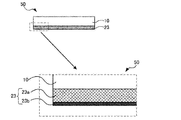
- FIG. 1 is a schematic view showing an example of a substrate 50 with a conductive film of the present invention.
- the substrate 50 with a conductive film of the present invention has a structure in which the back surface conductive film 23 is formed on the back surface of the mask blank substrate 10.
- the substrate 50 with a conductive film is a substrate in which the back surface conductive film 23 is formed at least on the back surface of the mask blank substrate 10, and the multilayer reflective film 21 is formed on another main surface.
- the conductive film-coated substrate 50 includes a substrate (multilayer reflective film-coated substrate 20) and a substrate on which the absorber film 24 is further formed (reflective mask blank 30).
- the back surface conductive film 23 may be simply referred to as the conductive film 23.
- FIG. 3 An example of the multilayer reflective film coated substrate 20 is shown in FIG.
- a multilayer reflective film 21 is formed on the main surface of the multilayer reflective film coated substrate 20 shown in FIG.
- FIG. 3 shows a multilayer reflective film coated substrate 20 having a back surface conductive film 23 formed on the back surface.
- the multilayer reflective film coated substrate 20 shown in FIG. 3 is a type of the conductive film coated substrate 50 because the back surface conductive film 23 is included on the back surface.
- FIG. 6 is a schematic view showing an example of the reflective mask blank 30 of the present invention.
- the reflective mask blank 30 of the present invention has a multilayer film 26 for mask blank on the main surface of the mask blank substrate 10.
- the mask blank multilayer film 26 includes the multilayer reflective film 21 and the absorber film 24 formed by laminating on the main surface of the mask blank substrate 10 in the reflective mask blank 30. It is a plurality of membranes.
- the mask blank multilayer film 26 further includes a protective film 22 formed between the multilayer reflective film 21 and the absorber film 24 and / or an etching mask film 25 formed on the surface of the absorber film 24 or the like. Can.
- the multilayer film 26 for mask blanks on the main surface of the mask blank substrate 10 comprises the multilayer reflective film 21, the protective film 22, the absorber film 24 and the etching mask film. It has 25.
- the etching mask film 25 may be peeled off after forming a transfer pattern on the absorber film 24 as described later.
- the absorber film 24 has a laminated structure of a plurality of layers, and the materials constituting the plurality of layers have different etching characteristics to provide an etching mask function. It is good also as a reflection type mask blank 30 used as the absorber film 24 which it had.
- the reflective mask blank 30 of the present invention includes a back surface conductive film 23 on the back surface. Therefore, the reflective mask blank 30 shown in FIG. 6 is a type of the substrate 50 with a conductive film.
- “having the multilayer reflective film 21 on the main surface of the mask blank substrate 10” means that the multilayer reflective film 21 is disposed in contact with the surface of the mask blank substrate 10. In addition to the case of including, it also includes the case of having another film between the mask blank substrate 10 and the multilayer reflective film 21. The same applies to the other films.
- “having the film B on the film A” means that the film A and the film B are disposed so as to be in direct contact with each other, and another film may be interposed between the film A and the film B. It also includes the case of having.
- the film A is disposed in contact with the surface of the film B” means that the film A and the film B are formed without interposing another film between the film A and the film B. Directly means that they are placed in contact with each other.
- “upper” may mean a direction away from the mask blank substrate 10.
- FIG. 4 is a schematic view showing another example of the reflective mask blank 30 of the present invention.
- the mask blank multilayer film 26 includes the multilayer reflective film 21, the protective film 22, and the absorber film 24 but does not include the etching mask film 25.
- the reflective mask blank 30 of FIG. 4 includes a back surface conductive film 23 on the back surface. Therefore, the reflective mask blank 30 shown in FIG. 4 is a kind of the substrate 50 with a conductive film.
- Rms (Root means square) which is a representative index of surface roughness is root mean square roughness, and is a square root of a value obtained by averaging the squares of deviation from the mean line to the measurement curve.
- Rms is expressed by the following equation (1).
- Equation (1) l is the reference length, and Z is the height from the mean line to the measurement curve.
- Rms is conventionally used to manage the surface roughness of the mask blank substrate 10, and the surface roughness can be grasped numerically.
- CTIR Coordinate Total Indicated Reading
- the surface shape can be performed using a surface shape analysis device (surface shape measurement device).
- a publicly known method can be used for the measuring method of surface shape. It is preferable to use a method of measuring the surface shape using interference fringes of the irradiated light because the surface shape can be measured with high accuracy in a short time.
- the inspection light having a strong tendency of laser light or the like is irradiated to the entire measurement region of the object to be measured, and the light reflected by the surface and the high flatness are provided. An interference fringe image is generated between the light reflected by the reference surface, and the interference fringe image is image-analyzed to acquire the surface shape of the substrate.
- an apparatus surface shape analysis apparatus
- UltraFLAT 200M manufactured by Corning TROPEL
- the measurement of the surface shape can be generally performed by the following method. First, measurement points are arranged in a grid on the surface of the measurement target, and height information of each measurement point (a reference plane at this time is, for example, a reference plane of the measurement apparatus) is acquired by the surface shape measurement apparatus. Do. Next, based on the height information of each measurement point, a plane (least square plane) approximated by the least square method is calculated, and this is used as a reference plane. Next, the height information of each measurement point described above is converted into the height of each measurement point with reference to the reference plane (least square plane), and the result is used as information on the surface shape at each measurement point. .
- the size of the measurement area of the surface shape can be appropriately selected depending on the size of the substrate, the size of the pattern when used as a reflective mask, the size of the electrostatic chuck, and the like.
- 132 mm ⁇ 132 nm is set as a measurement region.
- the substrate 50 with a conductive film, the substrate 20 with a multilayer reflective film, the reflective mask blank 30 and the reflective mask 40 of the present invention will be described more specifically.
- the substrate 50 with a conductive film, the substrate 20 with a multilayer reflective film, the reflective mask blank 30 and the mask blank substrate 10 used for the reflective mask 40 of the present invention (sometimes referred to simply as “substrate 10”) will be described. Do.
- the substrate 10 one having a low thermal expansion coefficient within the range of 0 ⁇ 5 ppb / ° C. is preferably used in order to prevent distortion of the absorber pattern 24a due to heat at the time of exposure to EUV light.
- a material having a low thermal expansion coefficient in this range for example, SiO 2 —TiO 2 based glass, multicomponent glass ceramics, etc. can be used.
- the first main surface on the side on which the transfer pattern (absorber pattern 24a described later) of the substrate 10 is formed is processed so as to have high flatness from the viewpoint of obtaining at least pattern transfer accuracy and positional accuracy.
- the flatness is preferably 0.1 ⁇ m or less, more preferably 0.05 ⁇ m or less, and still more preferably in a 132 mm ⁇ 132 mm region of the main surface on the side where the transfer pattern of the substrate 10 is formed. It is 0.03 ⁇ m or less.
- the second main surface opposite to the first main surface is a surface to be electrostatically chucked when being set in the exposure apparatus.
- the second main surface preferably has a flatness of 0.1 ⁇ m or less, more preferably 0.05 ⁇ m or less, and still more preferably 0.03 ⁇ m or less in a 132 mm ⁇ 132 mm area.
- the flatness on the second main surface side of the reflective mask blank 30 is preferably 1 ⁇ m or less, more preferably 0.5 ⁇ m or less, and still more preferably 0.3 ⁇ m or less in the 142 mm ⁇ 142 mm region. It is.
- the height of the surface smoothness of the substrate 10 is also a very important item.
- the surface roughness of the first main surface on which the absorber pattern 24a for transfer is formed is preferably 0.1 nm or less in root mean square roughness (RMS).
- RMS root mean square roughness
- the surface smoothness can be measured by an atomic force microscope.
- the substrate 10 preferably has high rigidity in order to prevent deformation due to film stress of a film (such as the multilayer reflective film 21) formed thereon.
- the substrate 10 preferably has a high Young's modulus of 65 GPa or more.
- the multilayer reflective film coated substrate 20 of the present invention can have a base film in contact with the surface of the substrate 10.
- the base film is a thin film formed between the substrate 10 and the multilayer reflective film 21.
- a material containing ruthenium or tantalum as a main component is preferably used.
- Ru metal alone or Ta metal alone may be used, or Ru or Ta may be titanium (Ti), niobium (Nb), molybdenum (Mo), zirconium (Zr), yttrium (Y), boron (B), lanthanum (La) Or a Ru alloy or a Ta alloy containing a metal such as cobalt (Co) and / or rhenium (Re).
- the film thickness of the base film can be set to a range that does not adversely affect the predetermined light transmittance of the back surface conductive film 23.
- the film thickness of the underlayer can be, for example, in the range of 1 nm to 10 nm.
- Multilayer reflective film coated substrate 20 Next, the multilayer reflective film coated substrate 20 that can be used for the conductive film coated substrate 50 and the reflective mask blank 30 of the present invention will be described below.
- FIG. 2 is a schematic view showing an example of a multilayer reflective film coated substrate 20 that can be used for the back surface conductive film 23 and the reflective mask blank 30 of the present invention.
- FIG. 3 is a schematic view of another example of the multilayer reflective film coated substrate 20 of the present invention. As shown in FIG. 3, when the multilayer reflective film coated substrate 20 has a predetermined back surface conductive film 23, the multilayer reflective film coated substrate 20 is a type of the back surface conductive film 23 of the present invention. In this specification, the multilayer reflective film coated substrate 20 shown in both FIG. 2 and FIG. 3 is referred to as the multilayer reflective film coated substrate 20 of the present embodiment.
- the multilayer reflective film coated substrate 20 of the present embodiment has a multilayer reflective film 21 in which high refractive index layers and low refractive index layers are alternately stacked on the main surface opposite to the side on which the back surface conductive film 23 is formed. Is formed.
- the multilayer reflective film coated substrate 20 of the present embodiment can reflect EUV light of a predetermined wavelength by having the predetermined multilayer reflective film 21.
- the multilayer reflective film 21 can be formed before the back surface conductive film 23 is formed.
- the back surface conductive film 23 may be formed as shown in FIG. 1, and then the multilayer reflective film 21 may be formed as shown in FIG.
- the multilayer reflective film 21 has a function of reflecting EUV light in the reflective mask 40.
- the multilayer reflective film 21 has a configuration of a multilayer film in which each layer containing an element having a different refractive index as a main component is periodically stacked.
- a multilayer film in which 40 to 60 cycles are alternately laminated is used.
- the multilayer film may be laminated in a plurality of cycles with a laminated structure of high refractive index layer / low refractive index layer in which a high refractive index layer and a low refractive index layer are laminated in this order from the substrate 10 side.
- the layer on the outermost surface of the multilayer reflective film 21 is preferably a high refractive index layer.
- the multilayer film described above when laminating a plurality of cycles with one cycle of a laminated structure (high refractive index layer / low refractive index layer) in which a high refractive index layer and a low refractive index layer are laminated in this order on the substrate 10, It becomes a low refractive index layer.
- the low refractive index layer on the outermost surface of the multilayer reflective film 21 is easily oxidized, so the reflectance of the multilayer reflective film 21 is reduced.
- the multi-layered film described above in the case of laminating a plurality of periods with one cycle being a laminated structure (low refractive index layer / high refractive index layer) in which low refractive index layers and high refractive index layers are laminated in this order on the substrate 10
- the uppermost layer is a high refractive index layer. In this case, it is not necessary to further form a high refractive index layer.
- a layer containing silicon (Si) is employed as the high refractive index layer.
- a material containing Si a Si compound containing boron (B), carbon (C), nitrogen (N), and / or oxygen (O) in addition to Si alone can be used.
- a layer containing Si as a high refractive index layer, a reflective mask 40 for EUV lithography excellent in the reflectivity of EUV light can be obtained.
- a glass substrate is preferably used as the substrate 10. Si is also excellent in adhesion to the glass substrate.
- the low refractive index layer a single metal selected from molybdenum (Mo), ruthenium (Ru), rhodium (Rh), and platinum (Pt), or an alloy of these metals is used.
- Mo molybdenum
- Ru ruthenium
- Rh rhodium
- Pt platinum
- the multilayer reflective film 21 for EUV light with a wavelength of 13 nm to 14 nm preferably, a Mo / Si periodic laminated film in which Mo films and Si films are alternately laminated for about 40 to 60 cycles is used.
- the high refractive index layer which is the uppermost layer of the multilayer reflective film 21 is formed of silicon (Si), and a silicon oxide containing silicon and oxygen between the uppermost layer (Si) and the Ru-based protective film 22. Layers can be formed. By forming the silicon oxide layer, the cleaning resistance of the reflective mask 40 can be improved.
- the reflectance of the multilayer reflective film 21 alone is usually 65% or more, and the upper limit is usually 73%.
- the thickness and period of each constituent layer of the multilayer reflective film 21 can be appropriately selected according to the exposure wavelength, and can be selected, for example, to satisfy the Bragg reflection law.
- a plurality of high refractive index layers and a plurality of low refractive index layers are present.
- the thicknesses of the plurality of high refractive index layers do not have to be the same, and the thicknesses of the plurality of low refractive index layers do not need to be the same.
- the film thickness of the Si layer on the outermost surface of the multilayer reflective film 21 can be adjusted within a range that does not reduce the reflectance.
- the film thickness of the outermost surface Si (high refractive index layer) can be 3 nm to 10 nm.
- the formation method of the multilayer reflective film 21 is known. For example, it can be formed by depositing each layer of the multilayer reflective film 21 by ion beam sputtering.
- a Si film of about 4 nm in thickness is first formed on the substrate 10 using an Si target by ion beam sputtering, for example, and then a thickness of 3 nm using an Mo target.
- the Mo film is deposited to a certain extent.
- the multilayer reflective film 21 is formed by stacking the Si film / Mo film for 40 to 60 cycles with one cycle (the outermost layer is a Si layer). Further, it is preferable to form the multilayer reflective film 21 by performing ion beam sputtering by supplying krypton (Kr) ion particles from an ion source when forming the multilayer reflective film 21.
- Kr krypton
- the mask blank multilayer film 26 is disposed on the surface of the multilayer reflective film 21 in contact with the surface opposite to the mask blank substrate 10. It is preferable to further include.
- the protective film 22 is formed on the multilayer reflective film 21 in order to protect the multilayer reflective film 21 from dry etching and cleaning in the manufacturing process of the reflective mask 40 described later. Further, the multilayer reflective film 21 can be protected by the protective film 22 at the time of black defect correction of the absorber pattern 24 a using an electron beam (EB).
- the protective film 22 can have a stacked structure of three or more layers.
- the lowermost layer and the uppermost layer of the protective film 22 are made of the above-described Ru-containing material, and a metal other than Ru or an alloy of a metal other than Ru is interposed between the lowermost layer and the uppermost layer. It can be structured.
- the material of the protective film 22 is made of, for example, a material containing ruthenium as a main component.
- an Ru metal alone or titanium (Ti), niobium (Nb), molybdenum (Mo), zirconium (Zr), yttrium (Y), boron (B), lanthanum (La) to Ru Ru alloys containing metals such as cobalt (Co), and / or rhenium (Re) can be used.
- the material of these protective films 22 can further contain nitrogen. The protective film 22 is effective when patterning the absorber film 24 by dry etching of a Cl-based gas.
- the Ru content ratio of the Ru alloy is 50 atomic% or more and less than 100 atomic%, preferably 80 atomic% or more and less than 100 atomic%, more preferably 95 atomic% or more and less than 100 atomic% It is.
- the Ru content ratio of the Ru alloy is 95 atomic percent or more and less than 100 atomic percent, the reflectance of the EUV light is reduced while suppressing the diffusion of the element (silicon) constituting the multilayer reflective film 21 to the protective film 22. It can be secured enough.
- the protective film 22 can have both mask cleaning resistance, an etching stopper function when the absorber film 24 is etched, and a protective function for preventing the multilayer reflective film 21 from changing with time.
- the EUV pellicle for preventing the adhesion of foreign matter on the mask pattern surface is not technically simple. From this, pellicle-less operation without using a pellicle has become mainstream. Further, in the case of EUV lithography, exposure contamination occurs such that a carbon film is deposited on a mask or an oxide film is grown by EUV exposure. Therefore, at the stage where the EUV reflective mask 40 is used for manufacturing a semiconductor device, it is necessary to perform frequent cleaning to remove foreign matter and contamination on the mask. For this reason, the EUV reflective mask 40 is required to have a mask cleaning resistance that is an order of magnitude greater than that of a transmissive mask for photolithography.
- the cleaning resistance to a cleaning solution such as sulfuric acid, sulfuric acid-hydrogen peroxide (SPM), ammonia, ammonia-hydrogen peroxide (APM), OH radical cleaning water and ozone water having a concentration of 10 ppm or less Can be particularly high. Therefore, it becomes possible to satisfy the mask cleaning resistance requirement for the EUV reflective mask 40.
- the thickness of the protective film 22 is not particularly limited as long as it can function as the protective film 22. From the viewpoint of the reflectance of EUV light, the thickness of the protective film 22 is preferably 1.0 nm to 8.0 nm, more preferably 1.5 nm to 6.0 nm.
- the same method as a known film forming method can be employed without particular limitation.
- sputtering method and ion beam sputtering method are mentioned.
- the substrate 50 with a conductive film of the present invention will be described.
- a predetermined back surface conductive film 23 is formed on the surface of the substrate 10 opposite to the surface in contact with the multilayer reflective film 21, as shown in FIG.
- a substrate 50 with a conductive film can be obtained.
- the substrate 50 with a conductive film of the present invention does not necessarily have to have the multilayer reflective film 21.
- the substrate 50 with a conductive film of the present invention can also be obtained by forming a predetermined back surface conductive film 23 on one surface of the main surface of the mask blank substrate 10.
- the conductive film 23 (back surface conductive film 23) is formed on one surface (back surface) on the main surface of the mask blank substrate 10 used for lithography.
- the conductive film 23 includes a transparent conductive layer 23a provided on the substrate side and an upper layer 23b provided on the transparent conductive layer 23a.
- the conductive film 23 has a transmittance of 10% or more for light with a wavelength of 532 nm.
- the upper layer 23 b is made of a material containing tantalum (Ta) and boron (B), and the film thickness of the upper layer is 0.5 nm or more and less than 10 nm.
- the upper layer 23 b is a film which is disposed in a direction away from the mask blank substrate 10 among the films constituting the conductive film 23.
- the conductive film 23 of the substrate 50 with a conductive film of the present invention includes a transparent conductive layer 23 a provided on the substrate 10 side.
- the material of the transparent conductive layer 23a may be any material as long as it has a predetermined transmittance for light of a wavelength of 532 nm and has a predetermined electric conductivity.
- a material of a transparent conductive film such as tin-doped indium oxide (ITO), fluorine-doped tin oxide (FTO), aluminum-doped zinc oxide (AZO) or antimony-doped tin oxide (ATO) Is preferred.
- the electrical characteristics (sheet resistance) required for the back surface conductive film 23 for electrostatic chuck can be 100 ⁇ / ⁇ ( ⁇ / square) or less.
- an ITO film with a film thickness of 100 nm has a transmittance of about 79.1% to light of a wavelength of 532 nm, and a sheet resistance of 50 ⁇ / ⁇ .
- the transparent conductive layer 23a is preferably made of a material containing titanium (Ti) and nitrogen (N).
- the transparent conductive layer 23a is made of a material containing titanium and nitrogen, so that it is possible to obtain the transparent conductive layer 23a having appropriate transmittance and conductivity.
- the total content of titanium and nitrogen in the material containing titanium and nitrogen is preferably 95 atomic% or more.
- the material containing titanium and nitrogen preferably contains more titanium than stoichiometric titanium nitride. That is, the ratio of atomic% of titanium and atomic% of nitrogen in the material of the transparent conductive layer 23a (atomic% of nitrogen / atomic% of titanium) is less than 1, preferably 0.95 or less, It is more preferable that it is 0.9 or less.
- the material of the transparent conductive layer 23a contains a relatively large amount of titanium, the electrical conductivity of the material of the transparent conductive layer 23a can be increased. Therefore, the sheet resistance of the transparent conductive layer 23a can be lowered.
- the transparent conductive layer 23a formed of a material containing titanium and nitrogen can be a uniform film in which the concentration of titanium and nitrogen is uniform, except for the surface layer affected by surface oxidation.
- a composition gradient film can be obtained in which the concentration of titanium and / or nitrogen in the transparent conductive layer 23a changes along the thickness direction of the transparent conductive layer 23a.
- the material containing titanium and nitrogen for forming the transparent conductive layer 23a can further contain a metal other than titanium as long as the effects of the present invention are not impaired.
- metals other than titanium include Ag, Au, Cu, Al, Mg, W and Co, which are highly conductive metals.
- the material containing titanium and nitrogen for forming the transparent conductive layer 23a does not contain nonmetals (for example, oxygen and boron etc.) other than nitrogen. In particular, when the material contains boron, both the transmittance and the conductivity decrease. Therefore, it is preferable that the material containing titanium and nitrogen for forming the transparent conductive layer 23a does not contain boron.
- the transparent conductive layer 23a of a material containing titanium and nitrogen has a value I (200) of the intensity of the diffraction peak of TiN (200) and an intensity of the diffraction peak of TiN (200) at the intensity of the diffraction peak by X-ray diffraction.
- the ratio (I r ) divided by the value of the sum of the value I (200) and the value I (111) of the intensity of the diffraction peak of TiN (111) is preferably 0.4 or more. Is more preferable, and 0.7 or more is more preferable.
- the value of the intensity of the diffraction peak of TiN (200) is increased compared to the value of the intensity of the diffraction peak of TiN (111). It can be said that the titanium content in the transparent conductive layer 23a is a desirable value when the ratio of the intensity values of the diffraction peaks of TiN (200) is not less than a predetermined ratio.
- strength of a diffraction peak is the intensity
- the intensity of the diffraction peak is a value proportional to the area of the predetermined diffraction peak.
- processing such as subtraction of a predetermined background can be performed.
- the intensities of the diffraction peaks of TiN (200) and TiN (111) can be measured as follows. That is, a characteristic X-ray of CuK ⁇ generated at a voltage of 45 kV and a current of 200 mA is irradiated to a sample using an X-ray diffractometer SmartLab (manufactured by RIGAKU Co., Ltd.) to measure the intensity and diffraction angle (2 ⁇ ) of the diffracted X-ray.
- the diffraction peak of the diffracted X-ray corresponding to the predetermined crystal plane can be obtained.
- the intensity of the diffraction peak can be determined by measuring the area of the predetermined peak. At that time, processing such as subtraction of a predetermined background can be performed using software attached to the measuring apparatus.
- the film thickness of the transparent conductive layer 23a of a material containing titanium and nitrogen is preferably 8 nm or more and 16 nm or less, more preferably 10 nm or more and 16 nm or less, and still more preferably 10 nm or more and 14 nm or less.
- the transparent conductive layer 23a of the material containing titanium and nitrogen has a predetermined film thickness, the transparent conductive layer 23a having more appropriate transmittance and conductivity can be obtained.
- the deformation amount (CTIR) of the substrate due to film stress is in the range of 350 ⁇ 150 nm, which is preferable.
- a material of the transparent conductive layer 23a having high transmittance and electrical conductivity a material containing at least one metal can be used.
- Metals that can be used as the material of the transparent conductive layer 23a are nickel (Ni), chromium (Cr), aluminum (Al), gold (Au), silver (Ag), copper (Cu), titanium (Ti), tungsten It can be at least one selected from (W), indium (In), platinum (Pt), molybdenum (Mo), rhodium (Rh), and zinc (Zn).
- the transparent conductive layer 23a made of a metal material has higher electric conductivity than a transparent conductive film such as ITO, and therefore, can be thinned.
- the film thickness of the transparent conductive layer 23a made of a metal material is preferably 50 nm or less, and more preferably 20 nm or less.
- the film thickness of the transparent conductive layer 23a of the metal material is preferably 2 nm or more from the viewpoint of stability at the time of film formation.
- a Pt film having a film thickness of 10.1 nm has a transmittance of 20.3% to light of a wavelength of 532 nm, and a sheet resistance of 25.3 ⁇ / ⁇ .
- the film thickness of the transparent conductive layer 23a can select a film thickness suitable for the relationship between the transmittance
- the thickness of the transparent conductive layer 23a of the substrate 50 with a conductive film of the present invention is preferably 6 nm or more and 30 nm or less.
- the conductive film 23 of the substrate 50 with a conductive film of the present invention includes an upper layer 23b provided on the opposite side of the transparent conductive layer 23a to the substrate 10 side.
- the back surface conductive film 23 includes the upper layer 23 b, the mechanical strength of the back surface conductive film 23 can be increased.
- the upper layer 23b of the conductive film 23 preferably has a smaller thickness than the transparent conductive layer 23a.
- the upper layer 23b is irradiated with a laser beam or the like to the substrate 10 to correct the displacement of the reflective mask 40. Absorption of the laser beam can be reduced.
- the upper layer 23 b of the back surface conductive film 23 is made of a material containing tantalum (Ta) and boron (B).
- Ta tantalum
- B boron
- the upper layer 23b of the TaB film on the transparent conductive layer 23a has the effect of making the surface smooth.
- the TiN film tends to have a large surface roughness because of its crystal structure. Since the TaB film is amorphous, it is possible to reduce the surface roughness of the back surface conductive film 23 by forming the film on the TiN film.
- the TaB film is poorly soluble in acid, it is resistant to washing with acid. Therefore, by using a TaB film as the upper layer 23b, even when the transparent conductive layer 23a is soluble in an acid, it is possible to obtain a reflective mask 40 having cleaning resistance.
- the TaB film be formed on the main surface of the substrate 10 in a region wider than the formation region of the transparent conductive layer 23 a. Since the side walls of the transparent conductive layer 23a are covered with the TaB film and the material of the transparent conductive layer 23a is not exposed, it is possible to obtain the reflective mask 40 having more excellent cleaning resistance.
- the upper layer 23b does not contain nitrogen and oxygen except in the case where it is unavoidably mixed and present at the time of film formation or the like.
- the composition of the film is a material containing only two types of Ta and B than a material further containing nitrogen and / or oxygen. It is because control of film conditions is easy. Therefore, it is preferable that the upper layer 23b does not contain nitrogen and oxygen.
- the crack generation load value described later can be made larger than 500 mN, which is preferable, and if it is 1.5 nm or more, the crack generation load It is more preferable because it can be larger than 1000 mN.
- the film thickness of the upper layer 23b is preferably less than 10 nm, and more preferably 5.5 nm or less. When the film thickness of the upper layer 23b is thinner than a predetermined film thickness, it becomes difficult to obtain desired mechanical strength. When the film thickness of the upper layer 23b is thicker than a predetermined film thickness, the transmittance of light of a predetermined wavelength of the back surface conductive film 23 is reduced, which makes it difficult to obtain the predetermined transmittance.
- the mechanical strength required of the back surface conductive film 23 can be obtained by setting the film thickness of the upper layer 23b made of a TaB film in the above range.
- the film thickness of the back surface conductive film 23 including the transparent conductive layer 23 a and the upper layer 23 b is preferably 10 nm or more and 22 nm or less, and more preferably 12 nm or more and 16 nm or less.
- the transmittance of the back surface conductive film 23 including the transparent conductive layer 23a and the upper layer 23b at a wavelength of 532 nm is 10% or more, preferably 20% or more, and more preferably 25% or more.
- the transmittance at a wavelength of 632 nm is preferably 25% or more.
- the transmittance of the conductive film 23 is transmitted through the conductive film 23 and the substrate 10 by irradiating the substrate 50 with the conductive film 23 with light having a wavelength of 532 nm or 632 nm from the conductive film 23 side. It is obtained by measuring the transmitted light.
- the sheet resistance of the conductive film 23 including the transparent conductive layer 23a and the upper layer 23b is preferably 210 ohms / square or less, more preferably 150 ohms / square or less, and still more preferably 130 ohms / square or less.
- the sheet resistance of the conductive film 23 can be controlled by adjusting the composition and thickness of the transparent conductive layer 23a and the upper layer 23b.
- the surface roughness (surface roughness of the upper layer 23b) of the conductive film 23 including the transparent conductive layer 23a and the upper layer 23b is a root mean square roughness (Rms) obtained by measuring an area of 10 ⁇ m ⁇ 10 ⁇ m with an atomic force microscope. Is preferably 0.6 nm or less, and more preferably 0.3 nm or less. Since the surface of the conductive film 23 has a predetermined root mean square roughness (Rms), generation of particles due to rubbing between the electrostatic chuck and the conductive film 23 can be prevented.
- the surface shape of the surface (the surface of the upper layer 23b) of the conductive film 23 including the transparent conductive layer 23a and the upper layer 23b is convex, and the deformation (CTIR) of the substrate due to film stress in a 132 mm ⁇ 132 mm region is preferably 350 nm. It is in the range of ⁇ 300 nm, more preferably in the range of 350 nm ⁇ 150 nm.
- the mechanical strength of the conductive film 23 including the transparent conductive layer 23 a and the upper layer 23 b can be evaluated by measuring the crack generation load of the substrate 50 with a conductive film. For example, in order to increase the moving speed of the stage on which the reflective mask is mounted in order to increase the production efficiency, the load on the conductive film 23 is increased, so the mechanical strength of the conductive film 23 needs to be increased. .
- the mechanical strength is preferably more than 500 mN, more preferably more than 700 mN, still more preferably more than 1000 mN, still more preferably more than 1300 mN, and particularly preferably more than 2000 mN.
- the formation method of the back surface conductive film 23 is known.
- the back surface conductive film 23 can be formed by using, for example, a target of a predetermined metal or alloy by a magnetron sputtering method or an ion beam sputtering method.
- a target of Ti is used, and Ar gas and N 2 gas are introduced as gas for sputtering.
- a TiN film with a low degree of nitriding can be obtained by adjusting the flow ratio of Ar gas to N 2 gas at the time of film formation and performing low-pressure film formation.
- the transparent conductive layer 23a and the upper layer 23b at a low pressure, the adhesion to the substrate can be increased, and the crack generation load can be increased.
- the method for forming the transparent conductive layer 23a and the upper layer 23b of the back surface conductive film 23 is such that the film-forming surface of the substrate 10 for forming the transparent conductive layer 23a or the upper layer 23b is directed upward and
- the sputtering target is rotated at a predetermined angle with respect to the deposition surface at a position where the central axis of the substrate 10 is rotated on the horizontal plane and a straight line parallel to the central axis of the substrate 10 passing through the center of the sputtering target.
- the transparent conductive layer 23 a or the upper layer 23 b can be formed by sputtering the facing sputtering target.
- the predetermined angle be an angle at which the tilt angle of the sputtering target is 5 degrees or more and 30 degrees or less.
- the gas pressure during sputtering film-forming is 0.03 Pa or more and 0.1 Pa or less.
- the reflective mask 40 can be manufactured using the substrate 50 with a conductive film of the present invention.
- the conductive film 23 of the substrate 50 with a conductive film of the present invention can transmit a laser beam or the like having a wavelength of 532 nm.
- the back surface conductive film 23 disposed on the substrate 50 with a conductive film of the present invention has high mechanical strength by including the predetermined upper layer 23 b. Therefore, according to the present invention, a conductive film for manufacturing the reflective mask 40 having high mechanical strength of the back surface conductive film 23 and capable of correcting positional deviation of the reflective mask 40 from the back surface side by a laser beam or the like.
- the attached substrate 50 can be obtained.
- FIG. 4 is a schematic view showing an example of the reflective mask blank 30 of the present invention.
- the reflective mask blank 30 of the present invention has a structure in which an absorber film 24 is formed on the multilayer reflective film 21 of the above-described multilayer reflective film coated substrate 20 or on the protective film 22.
- the reflective mask blank 30 can further have an etching mask film 25 and / or a resist film 32 on the absorber film 24 (see FIG. 8A).
- the reflective mask blank 30 has an absorber film 24 on the multilayer reflective film coated substrate 20 described above. That is, the absorber film 24 is formed on the multilayer reflective film 21 (on the protective film 22 when the protective film 22 is formed).
- the basic function of the absorber film 24 is to absorb EUV light.
- the absorber film 24 may be an absorber film 24 for absorbing EUV light, or may be an absorber film 24 having a phase shift function in consideration of the phase difference of EUV light.
- the absorber film 24 having a phase shift function is to absorb EUV light and reflect a part thereof to shift the phase.
- the portion where the absorber film 24 is formed absorbs the EUV light and reduces the light while having no adverse effect on the pattern transfer. To reflect some light. Further, in the region (field portion) where the absorber film 24 is not formed, the EUV light is reflected from the multilayer reflective film 21 through the protective film 22. Therefore, a desired phase difference is provided between the reflected light from the absorber film 24 having the phase shift function and the reflected light from the field portion.
- the absorber film 24 having a phase shift function is formed so that the phase difference between the reflected light from the absorber film 24 and the reflected light from the multilayer reflective film 21 is 170 degrees to 190 degrees.
- the light of inverted phase difference in the vicinity of 180 degrees interferes with each other at the pattern edge to improve the image contrast of the projected optical image.
- the resolution is increased, and various tolerances for exposure such as exposure latitude and focus tolerance can be increased.
- the absorber film 24 may be a single layer film or a multilayer film composed of a plurality of films (for example, a lower absorber film and an upper absorber film).
- a single layer film there is a feature that the number of processes at the time of mask blank manufacture can be reduced and the production efficiency is improved.
- the optical constant and the film thickness can be appropriately set so that the upper absorber film becomes an antireflective film at the time of mask pattern defect inspection using light. This improves the inspection sensitivity at the time of mask pattern defect inspection using light.
- O oxygen
- N nitrogen
- the temporal stability is improved.
- the absorber film 24 can be formed as a multilayer film.
- the range of adjustment on the optical surface can be enlarged by forming the absorber film 24 into a multilayer film, so that it is easy to obtain a desired reflectance. Become.
- the material of the absorber film 24 has a function of absorbing EUV light and can be processed by etching etc. (preferably, it can be etched by dry etching of chlorine (Cl) or fluorine (F) based gas), It is not particularly limited.
- etching etc. preferably, it can be etched by dry etching of chlorine (Cl) or fluorine (F) based gas
- a material having such a function tantalum (Ta) alone or a material containing Ta can be preferably used.
- a material containing Ta for example, a material containing Ta and B, a material containing Ta and N, a material containing Ta and B, and at least one of O and N, a material containing Ta and Si, Ta and Si And materials containing Ta and Ge, materials containing Ta, Ge and N, materials containing Ta and Pd, materials containing Ta and Ru, materials containing Ta and Ti, and the like can be mentioned.
- the absorber film 24 may be, for example, a single Ni, a material containing Ni, a single Cr, a material containing Cr, a single Ru, a material containing Ru, a single Pd, a material containing Pd, a single Mo, and a material containing Mo. And a material comprising at least one selected from the group consisting of
- the thickness of the absorber film 24 is preferably 30 nm to 100 nm.
- the absorber film 24 can be formed by a known method, for example, a magnetron sputtering method, an ion beam sputtering method, or the like.
- etching mask film 25 may be formed on the absorber film 24.
- a material of the etching mask film 25 a material having a high etching selectivity of the absorber film 24 to the etching mask film 25 is used.
- the etching selectivity of B to A refers to the ratio of the etching rate of A which is a layer (layer serving as a mask) which is not desired to be etched to B which is a layer which is desired to be etched.
- etching selectivity of B to A etching rate of B / etching rate of A.
- high selection ratio means that the value of the selection ratio as defined above is large with respect to the comparison object.
- the etching selectivity of the absorber film 24 to the etching mask film 25 is preferably 1.5 or more, and more preferably 3 or more.
- Materials having a high etching selectivity of the absorber film 24 to the etching mask film 25 include materials of chromium and a chromium compound. Therefore, when etching the absorber film 24 with a fluorine-based gas, materials of chromium and chromium compounds can be used.
- the chromium compound includes a material containing Cr and at least one element selected from N, O, C and H. When the absorber film 24 is etched with a chlorine-based gas substantially free of oxygen, materials of silicon and silicon compounds can be used.
- silicon compounds materials containing Si and at least one element selected from N, O, C and H, metal silicon containing metal in silicon and silicon compounds (metal silicide), and metal silicon compound (metal silicide (metal silicide) Materials such as compounds).
- metal silicon compound examples include materials containing a metal, Si, and at least one element selected from N, O, C, and H.
- the film thickness of the etching mask film 25 is desirably 3 nm or more from the viewpoint of obtaining a function as an etching mask for forming a transfer pattern on the absorber film 24 with high accuracy. Also, from the viewpoint of reducing the thickness of the resist film 32, the thickness of the etching mask film 25 is desirably 15 nm or less.
- FIG. 5 is a schematic view showing a reflective mask 40 according to the present embodiment.
- the reflective mask 40 of the present invention has a structure in which the absorber pattern 24 a is formed on the multilayer reflective film 21 or on the protective film 22 by patterning the absorber film 24 in the above-mentioned reflective mask blank 30. .
- the reflective mask 40 of the present embodiment when exposed to exposure light such as EUV light, the exposure light is absorbed at the portion of the surface of the reflective mask 40 where the absorber film 24 is present, and the other absorber film 24 is removed. In the exposed portion, the exposure light is reflected by the exposed protective film 22 and multilayer reflective film 21, so that it can be used as a reflective mask 40 for lithography.
- the reflective mask 40 of the present invention by having the absorber pattern 24 a on the multilayer reflective film 21 (or on the protective film 22), it is possible to transfer a predetermined pattern to a transferee using EUV light. it can.
- the transmittance of the predetermined wavelength of the reflective mask 40 according to the present invention is equal to or higher than the predetermined value, so the reflective mask according to the present invention may be a laser beam according to the method described in Patent Document 3 (Japanese Patent No. 5883249).
- Patent Document 3 Japanese Patent No. 5883249.
- the positional deviation of 40 can be corrected. Therefore, it can be said that the reflective mask 40 of the present invention can have a transfer pattern of high accuracy.
- a circuit pattern or the like based on the absorber pattern 24 a of the reflective mask 40 on a resist film 32 formed on a transfer target such as a semiconductor substrate by a lithography process using the reflective mask 40 described above and an exposure apparatus By transferring the transfer pattern and performing various other processes, it is possible to manufacture a semiconductor device in which various transfer patterns and the like are formed on a transfer target such as a semiconductor substrate.
- the present invention is a method of manufacturing a semiconductor device including the step of performing a lithography process using an exposure apparatus using the above-mentioned reflective mask 40 and forming a transfer pattern on a transfer target.
- a reflective mask capable of correcting the positional deviation of the reflective mask 40 from the back side by a laser beam or the like by the method described in Patent Document 3 (Japanese Patent No. 5883249). 40 can be used for the manufacture of semiconductor devices. Therefore, when the reflective mask 40 of the present invention is used for manufacturing a semiconductor device, it can be said that a semiconductor device having a fine and highly accurate transfer pattern can be manufactured.
- the substrate 50 with a conductive film of the example and the comparative example will be described.
- the substrate 10 for manufacturing the substrate 50 with a conductive film of the example and the comparative example was prepared as follows. That is, an SiO 2 -TiO 2 based glass substrate, which is a low thermal expansion glass substrate of 6025 size (about 152 mm ⁇ 152 mm ⁇ 6.35 mm) with both main surfaces of the first main surface and the second main surface polished, is prepared It was ten. Polishing comprising a rough polishing process, a precision polishing process, a local processing process, and a touch polishing process was performed to obtain a flat and smooth main surface.
- a transparent conductive layer 23a made of a TiN film was formed on the second main surface (rear surface) of the SiO 2 -TiO 2 glass substrate 10 by a magnetron sputtering (reactive sputtering) method under the following conditions.
- Table 1 shows the film thickness corresponding to the sample number.
- Deposition gas pressure 0.043 Pa
- An upper layer 23b made of a TaB film was formed on the surface of the transparent conductive layer 23a by a magnetron sputtering (reactive sputtering) method under the following conditions.
- Table 1 shows the film thickness corresponding to the sample number.
- Deposition gas Xe gas atmosphere (flow rate 2.5 sccm).
- Deposition gas pressure 0.019 Pa
- the unit mN), the surface roughness (Rms, unit: nm), and the amount of deformation of the substrate due to film stress (CTIR, nm) are shown in Table 2.
- CTIR film stress
- substrate 50 with a conductive film of an Example and a comparative example was measured for evaluation of mechanical strength.
- the schematic diagram for demonstrating the measurement of a crack generation load to FIG. 9 is shown.
- the crack generation load can be measured as follows. That is, the substrate 50 with a conductive film is placed on the stage 104 of the crack generation load measuring apparatus 100. Next, the indenter 102 is disposed in contact with the conductive film 23 of the substrate 50 with a conductive film.
- the indenter 102 has a structure capable of pressing the tip of the indenter 102 against the conductive film 23 by applying a predetermined load.
- the tip of the indenter 102 is shaped to have a predetermined radius of curvature.
- the stage 104 is moved at a predetermined speed while the load applied to the indenter 102 is increased at a predetermined speed.
- the load of the indenter 102 when a crack was generated in the conductive film 23 of the substrate 50 with a conductive film was taken as the crack generation load.
- the measurement conditions of the crack generation load are as follows. Initial load: 20mN Increase speed of load on indenter 102: 400 mN / min Movement speed of stage 104: 1 mm / min Indenter 102 type: Rockwell Radius of curvature of tip of indenter 102: 20 ⁇ m
- the samples of the examples of the present invention all had a crack initiation load exceeding 500 mN, and Samples 2 to 6, 9 to 12, 15 to 18 had a crack initiation load exceeding 1000 mN.
- the samples of the comparative example were all less than 500 mN, and at most 468 mN (sample 7). Therefore, it was revealed that the substrate with a conductive film 50 having high mechanical strength of the back surface conductive film 23 can be obtained by the present invention.
- Samples 5, 6, 8 to 12 and 14 to 18 satisfied the mechanical strength requirements and had a sheet resistance of 150 ⁇ / ⁇ or less.
- Samples 11 to 18 also meet the mechanical strength requirements and have a CTIR of 350 nm ⁇ 300 nm.
- Samples 2-6, 8-10 met the mechanical strength requirements and had a CTIR of 350 nm ⁇ 150 nm.
- the multilayer reflective film 21 and the protective film 22 are formed on the main surface (first main surface) of the substrate 10 on the side opposite to the side on which the back surface conductive film 23 of the substrate 50 with a conductive film manufactured as described above is formed.
- a multilayer reflective film coated substrate 20 was manufactured by forming
- a reflective mask blank 30 was manufactured by forming the absorber film 24 on the protective film 22 of the multilayer reflective film coated substrate 20.
- the multilayer reflective film coated substrate 20 and the reflective mask blank 30 were manufactured as follows.
- the multilayer reflective film 21 was formed on the main surface (first main surface) of the substrate 10 opposite to the side on which the back surface conductive film 23 was formed.
- the multilayer reflective film 21 formed on the substrate 10 is a periodic multilayer reflective film 21 made of Mo and Si in order to form the multilayer reflective film 21 suitable for EUV light with a wavelength of 13.5 nm.
- the multilayer reflective film 21 was formed by alternately laminating Mo layers and Si layers on the substrate 10 by ion beam sputtering in an Ar gas atmosphere using a Mo target and a Si target. First, a Si film was formed to a thickness of 4.2 nm, and then a Mo film was formed to a thickness of 2.8 nm.
- a Si film was formed to a thickness of 4.0 nm to form a multilayer reflective film 21.
- 40 cycles are used here, the present invention is not limited to this.
- 60 cycles may be used. In the case of 60 cycles, although the number of processes increases more than 40 cycles, the reflectivity for EUV light can be increased.
- a protective film 22 made of a Ru film was formed to a thickness of 2.5 nm by an ion beam sputtering method using a Ru target in an Ar gas atmosphere.
- the reflective mask blanks 30 of the example and the comparative example of the present invention were manufactured.
- an absorber film 24 was formed on the protective film 22 of the multilayer reflective film coated substrate 20 by DC magnetron sputtering.
- the absorber film 24 was used as the absorber film 24 of the laminated film which consists of two layers, the TaBN film which is an absorption layer, and the TaBO film which is a low reflection layer.
- a TaBN film was formed as an absorption layer by DC magnetron sputtering.
- a TaBO film (low reflection layer) containing Ta, B and O was further formed by DC magnetron sputtering.
- the reflective mask blanks 30 of the example and the comparative example were manufactured.
- FIG. 8 is a schematic cross-sectional view showing the process of manufacturing the reflective mask 40 from the reflective mask blank 30. As shown in FIG.
- What formed the resist film 32 by thickness of 150 nm on the absorber film 24 of the reflection type mask blank 30 of the above-mentioned Example and comparative example was made into the reflection type mask blank 30 (FIG. 8 (a)).
- a desired pattern was drawn (exposed) on the resist film 32, and further developed and rinsed to form a predetermined resist pattern 32a (FIG. 8 (b)).
- the absorber pattern 24a was formed by performing dry etching of the absorber film 24 using the resist pattern 32a as a mask (FIG. 8C).
- dry etching can be performed using a mixed gas of Cl 2 and He.
- the absorber film 24 is a laminated film composed of two layers of TaBN film and TaBO film, a mixed gas of chlorine (Cl 2) and oxygen (O 2) (chlorine (Cl 2) and oxygen (O 2
- the dry etching can be performed by the mixing ratio (flow rate ratio) of 8) to 2).
- the resist pattern 32a was removed by ashing or a resist stripping solution.
- wet cleaning using pure water (DIW) was performed to manufacture a reflective mask 40 (FIG. 8 (d)). If necessary, mask defect inspection can be performed after wet cleaning to appropriately perform mask defect correction.
- the conductive film 23 of the example of the present invention has a transmittance of 10% or more of light of 532 nm wavelength.
- positional deviation of the reflective mask 40 can be corrected by a laser beam or the like. Therefore, when the reflective mask 40 of the present invention is used for manufacturing a semiconductor device, it can be said that a semiconductor device having a fine and highly accurate transfer pattern can be manufactured.
- the conductive film 23 of the embodiment of the present invention is excellent in mechanical strength. Therefore, the conductive film 23 of the reflective mask 40 of the present invention is also excellent in mechanical strength.
- a reflective mask 40 having high mechanical strength of the back surface conductive film 23 and capable of correcting positional deviation of the reflective mask 40 from the back surface side by a laser beam or the like can be used for manufacturing a semiconductor device. Therefore, a semiconductor device having a fine and highly accurate transfer pattern can be manufactured.
- the reflective mask 40 manufactured in this example was set in an EUV exposure apparatus, and EUV exposure was performed on a wafer having a film to be processed and a resist film 32 formed on a semiconductor substrate. Then, the exposed resist film 32 is developed to form a resist pattern 32 a on the semiconductor substrate on which the film to be processed is formed.
- the resist pattern 32a is transferred to a film to be processed by etching, and various steps such as formation of an insulating film and a conductive film, introduction of a dopant, or annealing are performed to manufacture a semiconductor device having desired characteristics. It was possible.
- Mask blank substrate 20 Multilayer reflective film coated substrate 21 Multilayer reflective film 22 Protective film 23 Conductive film (rear surface conductive film) 23a transparent conductive layer 23b upper layer 24 absorber film 24a absorber pattern 25 etching mask film 26 multilayer film for mask blanks 30 reflective mask blank 32 resist film 32a resist pattern 40 reflective mask 50 substrate with conductive film 100 crack generation load measuring apparatus 102 indenter 104 stage
Landscapes
- Physics & Mathematics (AREA)
- General Physics & Mathematics (AREA)
- Preparing Plates And Mask In Photomechanical Process (AREA)
- Thin Film Transistor (AREA)
- Formation Of Insulating Films (AREA)
- Photovoltaic Devices (AREA)
Priority Applications (4)
| Application Number | Priority Date | Filing Date | Title |
|---|---|---|---|
| JP2019561646A JP7208163B2 (ja) | 2017-12-27 | 2018-12-21 | 導電膜付き基板、多層反射膜付き基板、反射型マスクブランク、反射型マスク及び半導体装置の製造方法 |
| KR1020207011177A KR102830574B1 (ko) | 2017-12-27 | 2018-12-21 | 도전막 부착 기판, 다층 반사막 부착 기판, 반사형 마스크 블랭크, 반사형 마스크 및 반도체 장치의 제조 방법 |
| US16/955,734 US11561463B2 (en) | 2017-12-27 | 2018-12-21 | Substrate with conductive film, substrate with multilayer reflective film, reflective mask blank, reflective mask, and semiconductor device manufacturing method |
| SG11202005918UA SG11202005918UA (en) | 2017-12-27 | 2018-12-21 | Substrate with conductive film, substrate with multilayer reflective film, reflective mask blank, reflective mask, and semiconductor device manufacturing method |
Applications Claiming Priority (2)
| Application Number | Priority Date | Filing Date | Title |
|---|---|---|---|
| JP2017251163 | 2017-12-27 | ||
| JP2017-251163 | 2017-12-27 |
Publications (1)
| Publication Number | Publication Date |
|---|---|
| WO2019131506A1 true WO2019131506A1 (ja) | 2019-07-04 |
Family
ID=67067319
Family Applications (1)
| Application Number | Title | Priority Date | Filing Date |
|---|---|---|---|
| PCT/JP2018/047246 Ceased WO2019131506A1 (ja) | 2017-12-27 | 2018-12-21 | 導電膜付き基板、多層反射膜付き基板、反射型マスクブランク、反射型マスク及び半導体装置の製造方法 |
Country Status (6)
| Country | Link |
|---|---|
| US (1) | US11561463B2 (https=) |
| JP (1) | JP7208163B2 (https=) |
| KR (1) | KR102830574B1 (https=) |
| SG (1) | SG11202005918UA (https=) |
| TW (1) | TWI786243B (https=) |
| WO (1) | WO2019131506A1 (https=) |
Cited By (4)
| Publication number | Priority date | Publication date | Assignee | Title |
|---|---|---|---|---|
| JP2021071685A (ja) * | 2019-11-01 | 2021-05-06 | 凸版印刷株式会社 | 反射型マスク及び反射型マスクの製造方法 |
| JP7556497B1 (ja) * | 2023-03-17 | 2024-09-26 | Agc株式会社 | Euvリソグラフィ用反射型マスクブランクおよび導電膜付き基板 |
| WO2024195577A1 (ja) * | 2023-03-17 | 2024-09-26 | Agc株式会社 | Euvリソグラフィ用反射型マスクブランクおよび導電膜付き基板 |
| TWI918414B (zh) | 2019-09-30 | 2026-03-11 | 日商Hoya股份有限公司 | 附多層反射膜之基板、反射型光罩基底、反射型光罩、與半導體裝置之製造方法 |
Families Citing this family (5)
| Publication number | Priority date | Publication date | Assignee | Title |
|---|---|---|---|---|
| KR102002441B1 (ko) | 2017-01-17 | 2019-07-23 | 호야 가부시키가이샤 | 반사형 마스크 블랭크, 반사형 마스크 및 그 제조 방법, 및 반도체 장치의 제조 방법 |
| JP7525354B2 (ja) * | 2020-09-28 | 2024-07-30 | 株式会社トッパンフォトマスク | 反射型フォトマスクブランク及び反射型フォトマスク |
| US20220137500A1 (en) * | 2020-10-30 | 2022-05-05 | AGC Inc. | Glass substrate for euvl, and mask blank for euvl |
| KR20220058424A (ko) * | 2020-10-30 | 2022-05-09 | 에이지씨 가부시키가이샤 | Euvl용 유리 기판, 및 euvl용 마스크 블랭크 |
| KR102638933B1 (ko) * | 2021-09-28 | 2024-02-22 | 에이지씨 가부시키가이샤 | Euv 리소그래피용 반사형 마스크 블랭크 및 도전막을 구비한 기판 |
Citations (5)
| Publication number | Priority date | Publication date | Assignee | Title |
|---|---|---|---|---|
| JP2002222764A (ja) * | 2000-11-22 | 2002-08-09 | Hoya Corp | 多層膜付き基板、露光用反射型マスクブランク、露光用反射型マスクおよびその製造方法、並びに半導体の製造方法 |
| JP2013225662A (ja) * | 2012-03-19 | 2013-10-31 | Hoya Corp | Euvリソグラフィー用多層反射膜付き基板及びeuvリソグラフィー用反射型マスクブランク、並びにeuvリソグラフィー用反射型マスク及び半導体装置の製造方法 |
| JP2015114356A (ja) * | 2013-12-09 | 2015-06-22 | Hoya株式会社 | 機能膜付き基板の製造方法、多層膜付き基板の製造方法、マスクブランクの製造方法、及び転写用マスクの製造方法 |
| JP2015215602A (ja) * | 2014-04-22 | 2015-12-03 | 旭硝子株式会社 | Euvリソグラフィ用反射型マスクブランク、該マスクブランク用の機能膜付基板および、それらの製造方法 |
| JP2017102475A (ja) * | 2017-02-06 | 2017-06-08 | 旭硝子株式会社 | Euvリソグラフィ用反射型マスクブランク、および、euvリソグラフィ用反射型マスク |
Family Cites Families (13)
| Publication number | Priority date | Publication date | Assignee | Title |
|---|---|---|---|---|
| US6737201B2 (en) | 2000-11-22 | 2004-05-18 | Hoya Corporation | Substrate with multilayer film, reflection type mask blank for exposure, reflection type mask for exposure and production method thereof as well as production method of semiconductor device |
| TW583503B (en) * | 2000-12-01 | 2004-04-11 | Kansai Paint Co Ltd | Method of forming conductive pattern |
| US7524593B2 (en) * | 2005-08-12 | 2009-04-28 | Semiconductor Energy Laboratory Co., Ltd. | Exposure mask |
| JP5082857B2 (ja) | 2005-12-12 | 2012-11-28 | 旭硝子株式会社 | Euvリソグラフィ用反射型マスクブランク、および該マスクブランク用の導電膜付基板 |
| US7678511B2 (en) | 2006-01-12 | 2010-03-16 | Asahi Glass Company, Limited | Reflective-type mask blank for EUV lithography |
| EP1993781A4 (en) * | 2006-02-03 | 2016-11-09 | Semiconductor Energy Lab Co Ltd | MANUFACTURING METHOD FOR MEMORY ELEMENT, LASER RADIATION APPARATUS AND LASER RADIATION METHOD |
| WO2008072706A1 (ja) | 2006-12-15 | 2008-06-19 | Asahi Glass Company, Limited | Euvリソグラフィ用反射型マスクブランク、および該マスクブランク用の機能膜付基板 |
| DE102011078927B4 (de) | 2010-07-12 | 2019-01-31 | Carl Zeiss Sms Ltd. | Verfahren zum Korrigieren von Fehlern einer photolithographischen Maske |
| EP2581789B1 (en) * | 2011-10-14 | 2020-04-29 | Fundació Institut de Ciències Fotòniques | Optically transparent and electrically conductive coatings and method for their deposition on a substrate |
| JP6039207B2 (ja) * | 2012-03-23 | 2016-12-07 | Hoya株式会社 | Euvリソグラフィー用多層反射膜付き基板の製造方法及びeuvリソグラフィー用反射型マスクブランクの製造方法、euvリソグラフィー用反射型マスクの製造方法、及び半導体装置の製造方法 |
| US10431354B2 (en) * | 2013-03-15 | 2019-10-01 | Guardian Glass, LLC | Methods for direct production of graphene on dielectric substrates, and associated articles/devices |
| JP6033987B1 (ja) * | 2014-12-19 | 2016-11-30 | Hoya株式会社 | マスクブランク用基板、マスクブランク及びこれらの製造方法、転写用マスクの製造方法並びに半導体デバイスの製造方法 |
| DE102015108569B4 (de) * | 2015-05-29 | 2020-10-08 | Advanced Mask Technology Center Gmbh & Co. Kg | Reflektierende Fotomaske und Reflexionstyp-Maskenrohling |
-
2018
- 2018-12-21 WO PCT/JP2018/047246 patent/WO2019131506A1/ja not_active Ceased
- 2018-12-21 SG SG11202005918UA patent/SG11202005918UA/en unknown
- 2018-12-21 TW TW107146312A patent/TWI786243B/zh active
- 2018-12-21 KR KR1020207011177A patent/KR102830574B1/ko active Active
- 2018-12-21 JP JP2019561646A patent/JP7208163B2/ja active Active
- 2018-12-21 US US16/955,734 patent/US11561463B2/en active Active
Patent Citations (5)
| Publication number | Priority date | Publication date | Assignee | Title |
|---|---|---|---|---|
| JP2002222764A (ja) * | 2000-11-22 | 2002-08-09 | Hoya Corp | 多層膜付き基板、露光用反射型マスクブランク、露光用反射型マスクおよびその製造方法、並びに半導体の製造方法 |
| JP2013225662A (ja) * | 2012-03-19 | 2013-10-31 | Hoya Corp | Euvリソグラフィー用多層反射膜付き基板及びeuvリソグラフィー用反射型マスクブランク、並びにeuvリソグラフィー用反射型マスク及び半導体装置の製造方法 |
| JP2015114356A (ja) * | 2013-12-09 | 2015-06-22 | Hoya株式会社 | 機能膜付き基板の製造方法、多層膜付き基板の製造方法、マスクブランクの製造方法、及び転写用マスクの製造方法 |
| JP2015215602A (ja) * | 2014-04-22 | 2015-12-03 | 旭硝子株式会社 | Euvリソグラフィ用反射型マスクブランク、該マスクブランク用の機能膜付基板および、それらの製造方法 |
| JP2017102475A (ja) * | 2017-02-06 | 2017-06-08 | 旭硝子株式会社 | Euvリソグラフィ用反射型マスクブランク、および、euvリソグラフィ用反射型マスク |
Cited By (8)
| Publication number | Priority date | Publication date | Assignee | Title |
|---|---|---|---|---|
| TWI918414B (zh) | 2019-09-30 | 2026-03-11 | 日商Hoya股份有限公司 | 附多層反射膜之基板、反射型光罩基底、反射型光罩、與半導體裝置之製造方法 |
| JP2021071685A (ja) * | 2019-11-01 | 2021-05-06 | 凸版印刷株式会社 | 反射型マスク及び反射型マスクの製造方法 |
| JP7610346B2 (ja) | 2019-11-01 | 2025-01-08 | テクセンドフォトマスク株式会社 | 反射型マスク及び反射型マスクの製造方法 |
| JP7556497B1 (ja) * | 2023-03-17 | 2024-09-26 | Agc株式会社 | Euvリソグラフィ用反射型マスクブランクおよび導電膜付き基板 |
| WO2024195577A1 (ja) * | 2023-03-17 | 2024-09-26 | Agc株式会社 | Euvリソグラフィ用反射型マスクブランクおよび導電膜付き基板 |
| JP2024167411A (ja) * | 2023-03-17 | 2024-12-03 | Agc株式会社 | Euvリソグラフィ用反射型マスクブランクおよび導電膜付き基板 |
| US12339580B2 (en) | 2023-03-17 | 2025-06-24 | AGC Inc. | Reflective mask blank for EUV lithography and substrate equipped with conductive film |
| JP7708288B2 (ja) | 2023-03-17 | 2025-07-15 | Agc株式会社 | Euvリソグラフィ用反射型マスクブランクおよび導電膜付き基板 |
Also Published As
| Publication number | Publication date |
|---|---|
| TW201928506A (zh) | 2019-07-16 |
| TWI786243B (zh) | 2022-12-11 |
| SG11202005918UA (en) | 2020-07-29 |
| US20210103209A1 (en) | 2021-04-08 |
| KR20200100604A (ko) | 2020-08-26 |
| JP7208163B2 (ja) | 2023-01-18 |
| US11561463B2 (en) | 2023-01-24 |
| JPWO2019131506A1 (ja) | 2020-12-10 |
| KR102830574B1 (ko) | 2025-07-07 |
Similar Documents
| Publication | Publication Date | Title |
|---|---|---|
| JP7208163B2 (ja) | 導電膜付き基板、多層反射膜付き基板、反射型マスクブランク、反射型マスク及び半導体装置の製造方法 | |
| JP2025113408A (ja) | 反射型マスクブランク、反射型マスク及びその製造方法、並びに半導体装置の製造方法 | |
| US20220299862A1 (en) | Reflective mask blank for euv lithography, reflective mask for euv lithography, and method for manufacturing mask blank and mask | |
| JPWO2018135468A1 (ja) | 導電膜付き基板、多層反射膜付き基板、反射型マスクブランク、反射型マスク及び半導体装置の製造方法 | |
| JP6422873B2 (ja) | 多層反射膜付き基板、euvリソグラフィー用反射型マスクブランク、euvリソグラフィー用反射型マスク及びその製造方法、並びに半導体装置の製造方法 | |
| JP7569428B2 (ja) | 導電膜付基板、反射型マスクブランク及び反射型マスク、並びに半導体デバイスの製造方法 | |
| JP2022024617A (ja) | Euvリソグラフィ用反射型マスクブランク、euvリソグラフィ用反射型マスク、およびそれらの製造方法 | |
| JP7061715B2 (ja) | 多層反射膜付き基板、反射型マスクブランク、反射型マスク、及び半導体デバイスの製造方法 | |
| JP7746160B2 (ja) | 多層反射膜付き基板、反射型マスクブランク、反射型マスク、及び半導体装置の製造方法 | |
| JP2025076473A (ja) | マスクブランク、反射型マスク、および半導体デバイスの製造方法 | |
| KR102645567B1 (ko) | Euv 리소그래피용 반사형 마스크 블랭크, euv 리소그래피용 반사형 마스크 및 그것들의 제조 방법 | |
| JP6223756B2 (ja) | 多層反射膜付き基板、euvリソグラフィー用反射型マスクブランク、euvリソグラフィー用反射型マスク及びその製造方法、並びに半導体装置の製造方法 | |
| JP6855645B1 (ja) | 薄膜付基板、多層反射膜付基板、反射型マスクブランク、反射型マスク及び半導体装置の製造方法 | |
| JP6864952B2 (ja) | 導電膜付き基板、多層反射膜付き基板、反射型マスクブランク、反射型マスク及び半導体装置の製造方法 | |
| KR20250076524A (ko) | 도전막 부착 기판, 반사형 마스크 블랭크, 반사형 마스크 및 반도체 장치의 제조 방법 | |
| JP7697609B1 (ja) | 反射型マスクブランク、反射型マスクブランクの製造方法、反射型マスク、反射型マスクの製造方法 | |
| JP2019191209A (ja) | 導電膜付き基板、多層反射膜付き基板、反射型マスクブランク、反射型マスク及び半導体装置の製造方法 | |
| KR20250151382A (ko) | 반사형 마스크 블랭크, 반사형 마스크 및 반도체 디바이스의 제조 방법 | |
| WO2024085089A1 (ja) | 反射型マスクブランク、反射型マスク、反射型マスクの製造方法 | |
| WO2025205962A1 (ja) | 多層反射膜付き基板、反射型マスクブランク、反射型マスク、及び半導体装置の製造方法 | |
| KR20240089139A (ko) | 다층 반사막 부착 기판, 반사형 마스크 블랭크 및 반사형 마스크, 그리고 반도체 장치의 제조 방법 |
Legal Events
| Date | Code | Title | Description |
|---|---|---|---|
| 121 | Ep: the epo has been informed by wipo that ep was designated in this application |
Ref document number: 18896978 Country of ref document: EP Kind code of ref document: A1 |
|
| ENP | Entry into the national phase |
Ref document number: 2019561646 Country of ref document: JP Kind code of ref document: A |
|
| ENP | Entry into the national phase |
Ref document number: 20207011177 Country of ref document: KR Kind code of ref document: A |
|
| NENP | Non-entry into the national phase |
Ref country code: DE |
|
| 122 | Ep: pct application non-entry in european phase |
Ref document number: 18896978 Country of ref document: EP Kind code of ref document: A1 |