WO2019131490A1 - Procédé pour lier un substrat, stratifié de substrats transparent, et dispositif comportant un stratifié de substrats - Google Patents
Procédé pour lier un substrat, stratifié de substrats transparent, et dispositif comportant un stratifié de substrats Download PDFInfo
- Publication number
- WO2019131490A1 WO2019131490A1 PCT/JP2018/047204 JP2018047204W WO2019131490A1 WO 2019131490 A1 WO2019131490 A1 WO 2019131490A1 JP 2018047204 W JP2018047204 W JP 2018047204W WO 2019131490 A1 WO2019131490 A1 WO 2019131490A1
- Authority
- WO
- WIPO (PCT)
- Prior art keywords
- substrate
- bonding
- substrates
- metal oxide
- thin film
- Prior art date
Links
Images


Classifications
-
- C—CHEMISTRY; METALLURGY
- C03—GLASS; MINERAL OR SLAG WOOL
- C03C—CHEMICAL COMPOSITION OF GLASSES, GLAZES OR VITREOUS ENAMELS; SURFACE TREATMENT OF GLASS; SURFACE TREATMENT OF FIBRES OR FILAMENTS MADE FROM GLASS, MINERALS OR SLAGS; JOINING GLASS TO GLASS OR OTHER MATERIALS
- C03C27/00—Joining pieces of glass to pieces of other inorganic material; Joining glass to glass other than by fusing
- C03C27/06—Joining glass to glass by processes other than fusing
- C03C27/10—Joining glass to glass by processes other than fusing with the aid of adhesive specially adapted for that purpose
-
- B—PERFORMING OPERATIONS; TRANSPORTING
- B32—LAYERED PRODUCTS
- B32B—LAYERED PRODUCTS, i.e. PRODUCTS BUILT-UP OF STRATA OF FLAT OR NON-FLAT, e.g. CELLULAR OR HONEYCOMB, FORM
- B32B37/00—Methods or apparatus for laminating, e.g. by curing or by ultrasonic bonding
- B32B37/14—Methods or apparatus for laminating, e.g. by curing or by ultrasonic bonding characterised by the properties of the layers
- B32B37/26—Methods or apparatus for laminating, e.g. by curing or by ultrasonic bonding characterised by the properties of the layers with at least one layer which influences the bonding during the lamination process, e.g. release layers or pressure equalising layers
-
- B—PERFORMING OPERATIONS; TRANSPORTING
- B29—WORKING OF PLASTICS; WORKING OF SUBSTANCES IN A PLASTIC STATE IN GENERAL
- B29C—SHAPING OR JOINING OF PLASTICS; SHAPING OF MATERIAL IN A PLASTIC STATE, NOT OTHERWISE PROVIDED FOR; AFTER-TREATMENT OF THE SHAPED PRODUCTS, e.g. REPAIRING
- B29C59/00—Surface shaping of articles, e.g. embossing; Apparatus therefor
- B29C59/14—Surface shaping of articles, e.g. embossing; Apparatus therefor by plasma treatment
-
- B—PERFORMING OPERATIONS; TRANSPORTING
- B32—LAYERED PRODUCTS
- B32B—LAYERED PRODUCTS, i.e. PRODUCTS BUILT-UP OF STRATA OF FLAT OR NON-FLAT, e.g. CELLULAR OR HONEYCOMB, FORM
- B32B17/00—Layered products essentially comprising sheet glass, or glass, slag, or like fibres
- B32B17/06—Layered products essentially comprising sheet glass, or glass, slag, or like fibres comprising glass as the main or only constituent of a layer, next to another layer of a specific material
- B32B17/10—Layered products essentially comprising sheet glass, or glass, slag, or like fibres comprising glass as the main or only constituent of a layer, next to another layer of a specific material of synthetic resin
-
- B—PERFORMING OPERATIONS; TRANSPORTING
- B32—LAYERED PRODUCTS
- B32B—LAYERED PRODUCTS, i.e. PRODUCTS BUILT-UP OF STRATA OF FLAT OR NON-FLAT, e.g. CELLULAR OR HONEYCOMB, FORM
- B32B27/00—Layered products comprising a layer of synthetic resin
- B32B27/06—Layered products comprising a layer of synthetic resin as the main or only constituent of a layer, which is next to another layer of the same or of a different material
- B32B27/08—Layered products comprising a layer of synthetic resin as the main or only constituent of a layer, which is next to another layer of the same or of a different material of synthetic resin
-
- B—PERFORMING OPERATIONS; TRANSPORTING
- B32—LAYERED PRODUCTS
- B32B—LAYERED PRODUCTS, i.e. PRODUCTS BUILT-UP OF STRATA OF FLAT OR NON-FLAT, e.g. CELLULAR OR HONEYCOMB, FORM
- B32B27/00—Layered products comprising a layer of synthetic resin
- B32B27/28—Layered products comprising a layer of synthetic resin comprising synthetic resins not wholly covered by any one of the sub-groups B32B27/30 - B32B27/42
- B32B27/281—Layered products comprising a layer of synthetic resin comprising synthetic resins not wholly covered by any one of the sub-groups B32B27/30 - B32B27/42 comprising polyimides
-
- B—PERFORMING OPERATIONS; TRANSPORTING
- B32—LAYERED PRODUCTS
- B32B—LAYERED PRODUCTS, i.e. PRODUCTS BUILT-UP OF STRATA OF FLAT OR NON-FLAT, e.g. CELLULAR OR HONEYCOMB, FORM
- B32B27/00—Layered products comprising a layer of synthetic resin
- B32B27/32—Layered products comprising a layer of synthetic resin comprising polyolefins
- B32B27/325—Layered products comprising a layer of synthetic resin comprising polyolefins comprising polycycloolefins
-
- B—PERFORMING OPERATIONS; TRANSPORTING
- B32—LAYERED PRODUCTS
- B32B—LAYERED PRODUCTS, i.e. PRODUCTS BUILT-UP OF STRATA OF FLAT OR NON-FLAT, e.g. CELLULAR OR HONEYCOMB, FORM
- B32B27/00—Layered products comprising a layer of synthetic resin
- B32B27/36—Layered products comprising a layer of synthetic resin comprising polyesters
- B32B27/365—Layered products comprising a layer of synthetic resin comprising polyesters comprising polycarbonates
-
- B—PERFORMING OPERATIONS; TRANSPORTING
- B32—LAYERED PRODUCTS
- B32B—LAYERED PRODUCTS, i.e. PRODUCTS BUILT-UP OF STRATA OF FLAT OR NON-FLAT, e.g. CELLULAR OR HONEYCOMB, FORM
- B32B37/00—Methods or apparatus for laminating, e.g. by curing or by ultrasonic bonding
- B32B37/14—Methods or apparatus for laminating, e.g. by curing or by ultrasonic bonding characterised by the properties of the layers
- B32B37/24—Methods or apparatus for laminating, e.g. by curing or by ultrasonic bonding characterised by the properties of the layers with at least one layer not being coherent before laminating, e.g. made up from granular material sprinkled onto a substrate
-
- B—PERFORMING OPERATIONS; TRANSPORTING
- B32—LAYERED PRODUCTS
- B32B—LAYERED PRODUCTS, i.e. PRODUCTS BUILT-UP OF STRATA OF FLAT OR NON-FLAT, e.g. CELLULAR OR HONEYCOMB, FORM
- B32B38/00—Ancillary operations in connection with laminating processes
- B32B38/0008—Electrical discharge treatment, e.g. corona, plasma treatment; wave energy or particle radiation
-
- B—PERFORMING OPERATIONS; TRANSPORTING
- B32—LAYERED PRODUCTS
- B32B—LAYERED PRODUCTS, i.e. PRODUCTS BUILT-UP OF STRATA OF FLAT OR NON-FLAT, e.g. CELLULAR OR HONEYCOMB, FORM
- B32B38/00—Ancillary operations in connection with laminating processes
- B32B38/0036—Heat treatment
-
- B—PERFORMING OPERATIONS; TRANSPORTING
- B32—LAYERED PRODUCTS
- B32B—LAYERED PRODUCTS, i.e. PRODUCTS BUILT-UP OF STRATA OF FLAT OR NON-FLAT, e.g. CELLULAR OR HONEYCOMB, FORM
- B32B7/00—Layered products characterised by the relation between layers; Layered products characterised by the relative orientation of features between layers, or by the relative values of a measurable parameter between layers, i.e. products comprising layers having different physical, chemical or physicochemical properties; Layered products characterised by the interconnection of layers
- B32B7/04—Interconnection of layers
- B32B7/12—Interconnection of layers using interposed adhesives or interposed materials with bonding properties
-
- C—CHEMISTRY; METALLURGY
- C03—GLASS; MINERAL OR SLAG WOOL
- C03C—CHEMICAL COMPOSITION OF GLASSES, GLAZES OR VITREOUS ENAMELS; SURFACE TREATMENT OF GLASS; SURFACE TREATMENT OF FIBRES OR FILAMENTS MADE FROM GLASS, MINERALS OR SLAGS; JOINING GLASS TO GLASS OR OTHER MATERIALS
- C03C17/00—Surface treatment of glass, not in the form of fibres or filaments, by coating
- C03C17/22—Surface treatment of glass, not in the form of fibres or filaments, by coating with other inorganic material
- C03C17/23—Oxides
- C03C17/245—Oxides by deposition from the vapour phase
-
- C—CHEMISTRY; METALLURGY
- C03—GLASS; MINERAL OR SLAG WOOL
- C03C—CHEMICAL COMPOSITION OF GLASSES, GLAZES OR VITREOUS ENAMELS; SURFACE TREATMENT OF GLASS; SURFACE TREATMENT OF FIBRES OR FILAMENTS MADE FROM GLASS, MINERALS OR SLAGS; JOINING GLASS TO GLASS OR OTHER MATERIALS
- C03C27/00—Joining pieces of glass to pieces of other inorganic material; Joining glass to glass other than by fusing
- C03C27/04—Joining glass to metal by means of an interlayer
- C03C27/042—Joining glass to metal by means of an interlayer consisting of a combination of materials selected from glass, glass-ceramic or ceramic material with metals, metal oxides or metal salts
-
- C—CHEMISTRY; METALLURGY
- C03—GLASS; MINERAL OR SLAG WOOL
- C03C—CHEMICAL COMPOSITION OF GLASSES, GLAZES OR VITREOUS ENAMELS; SURFACE TREATMENT OF GLASS; SURFACE TREATMENT OF FIBRES OR FILAMENTS MADE FROM GLASS, MINERALS OR SLAGS; JOINING GLASS TO GLASS OR OTHER MATERIALS
- C03C27/00—Joining pieces of glass to pieces of other inorganic material; Joining glass to glass other than by fusing
- C03C27/06—Joining glass to glass by processes other than fusing
-
- C—CHEMISTRY; METALLURGY
- C23—COATING METALLIC MATERIAL; COATING MATERIAL WITH METALLIC MATERIAL; CHEMICAL SURFACE TREATMENT; DIFFUSION TREATMENT OF METALLIC MATERIAL; COATING BY VACUUM EVAPORATION, BY SPUTTERING, BY ION IMPLANTATION OR BY CHEMICAL VAPOUR DEPOSITION, IN GENERAL; INHIBITING CORROSION OF METALLIC MATERIAL OR INCRUSTATION IN GENERAL
- C23C—COATING METALLIC MATERIAL; COATING MATERIAL WITH METALLIC MATERIAL; SURFACE TREATMENT OF METALLIC MATERIAL BY DIFFUSION INTO THE SURFACE, BY CHEMICAL CONVERSION OR SUBSTITUTION; COATING BY VACUUM EVAPORATION, BY SPUTTERING, BY ION IMPLANTATION OR BY CHEMICAL VAPOUR DEPOSITION, IN GENERAL
- C23C14/00—Coating by vacuum evaporation, by sputtering or by ion implantation of the coating forming material
- C23C14/0021—Reactive sputtering or evaporation
- C23C14/0036—Reactive sputtering
-
- C—CHEMISTRY; METALLURGY
- C23—COATING METALLIC MATERIAL; COATING MATERIAL WITH METALLIC MATERIAL; CHEMICAL SURFACE TREATMENT; DIFFUSION TREATMENT OF METALLIC MATERIAL; COATING BY VACUUM EVAPORATION, BY SPUTTERING, BY ION IMPLANTATION OR BY CHEMICAL VAPOUR DEPOSITION, IN GENERAL; INHIBITING CORROSION OF METALLIC MATERIAL OR INCRUSTATION IN GENERAL
- C23C—COATING METALLIC MATERIAL; COATING MATERIAL WITH METALLIC MATERIAL; SURFACE TREATMENT OF METALLIC MATERIAL BY DIFFUSION INTO THE SURFACE, BY CHEMICAL CONVERSION OR SUBSTITUTION; COATING BY VACUUM EVAPORATION, BY SPUTTERING, BY ION IMPLANTATION OR BY CHEMICAL VAPOUR DEPOSITION, IN GENERAL
- C23C14/00—Coating by vacuum evaporation, by sputtering or by ion implantation of the coating forming material
- C23C14/02—Pretreatment of the material to be coated
- C23C14/021—Cleaning or etching treatments
- C23C14/022—Cleaning or etching treatments by means of bombardment with energetic particles or radiation
-
- C—CHEMISTRY; METALLURGY
- C23—COATING METALLIC MATERIAL; COATING MATERIAL WITH METALLIC MATERIAL; CHEMICAL SURFACE TREATMENT; DIFFUSION TREATMENT OF METALLIC MATERIAL; COATING BY VACUUM EVAPORATION, BY SPUTTERING, BY ION IMPLANTATION OR BY CHEMICAL VAPOUR DEPOSITION, IN GENERAL; INHIBITING CORROSION OF METALLIC MATERIAL OR INCRUSTATION IN GENERAL
- C23C—COATING METALLIC MATERIAL; COATING MATERIAL WITH METALLIC MATERIAL; SURFACE TREATMENT OF METALLIC MATERIAL BY DIFFUSION INTO THE SURFACE, BY CHEMICAL CONVERSION OR SUBSTITUTION; COATING BY VACUUM EVAPORATION, BY SPUTTERING, BY ION IMPLANTATION OR BY CHEMICAL VAPOUR DEPOSITION, IN GENERAL
- C23C14/00—Coating by vacuum evaporation, by sputtering or by ion implantation of the coating forming material
- C23C14/04—Coating on selected surface areas, e.g. using masks
- C23C14/042—Coating on selected surface areas, e.g. using masks using masks
-
- C—CHEMISTRY; METALLURGY
- C23—COATING METALLIC MATERIAL; COATING MATERIAL WITH METALLIC MATERIAL; CHEMICAL SURFACE TREATMENT; DIFFUSION TREATMENT OF METALLIC MATERIAL; COATING BY VACUUM EVAPORATION, BY SPUTTERING, BY ION IMPLANTATION OR BY CHEMICAL VAPOUR DEPOSITION, IN GENERAL; INHIBITING CORROSION OF METALLIC MATERIAL OR INCRUSTATION IN GENERAL
- C23C—COATING METALLIC MATERIAL; COATING MATERIAL WITH METALLIC MATERIAL; SURFACE TREATMENT OF METALLIC MATERIAL BY DIFFUSION INTO THE SURFACE, BY CHEMICAL CONVERSION OR SUBSTITUTION; COATING BY VACUUM EVAPORATION, BY SPUTTERING, BY ION IMPLANTATION OR BY CHEMICAL VAPOUR DEPOSITION, IN GENERAL
- C23C14/00—Coating by vacuum evaporation, by sputtering or by ion implantation of the coating forming material
- C23C14/06—Coating by vacuum evaporation, by sputtering or by ion implantation of the coating forming material characterised by the coating material
- C23C14/08—Oxides
- C23C14/081—Oxides of aluminium, magnesium or beryllium
-
- C—CHEMISTRY; METALLURGY
- C23—COATING METALLIC MATERIAL; COATING MATERIAL WITH METALLIC MATERIAL; CHEMICAL SURFACE TREATMENT; DIFFUSION TREATMENT OF METALLIC MATERIAL; COATING BY VACUUM EVAPORATION, BY SPUTTERING, BY ION IMPLANTATION OR BY CHEMICAL VAPOUR DEPOSITION, IN GENERAL; INHIBITING CORROSION OF METALLIC MATERIAL OR INCRUSTATION IN GENERAL
- C23C—COATING METALLIC MATERIAL; COATING MATERIAL WITH METALLIC MATERIAL; SURFACE TREATMENT OF METALLIC MATERIAL BY DIFFUSION INTO THE SURFACE, BY CHEMICAL CONVERSION OR SUBSTITUTION; COATING BY VACUUM EVAPORATION, BY SPUTTERING, BY ION IMPLANTATION OR BY CHEMICAL VAPOUR DEPOSITION, IN GENERAL
- C23C14/00—Coating by vacuum evaporation, by sputtering or by ion implantation of the coating forming material
- C23C14/22—Coating by vacuum evaporation, by sputtering or by ion implantation of the coating forming material characterised by the process of coating
- C23C14/56—Apparatus specially adapted for continuous coating; Arrangements for maintaining the vacuum, e.g. vacuum locks
-
- C—CHEMISTRY; METALLURGY
- C23—COATING METALLIC MATERIAL; COATING MATERIAL WITH METALLIC MATERIAL; CHEMICAL SURFACE TREATMENT; DIFFUSION TREATMENT OF METALLIC MATERIAL; COATING BY VACUUM EVAPORATION, BY SPUTTERING, BY ION IMPLANTATION OR BY CHEMICAL VAPOUR DEPOSITION, IN GENERAL; INHIBITING CORROSION OF METALLIC MATERIAL OR INCRUSTATION IN GENERAL
- C23C—COATING METALLIC MATERIAL; COATING MATERIAL WITH METALLIC MATERIAL; SURFACE TREATMENT OF METALLIC MATERIAL BY DIFFUSION INTO THE SURFACE, BY CHEMICAL CONVERSION OR SUBSTITUTION; COATING BY VACUUM EVAPORATION, BY SPUTTERING, BY ION IMPLANTATION OR BY CHEMICAL VAPOUR DEPOSITION, IN GENERAL
- C23C14/00—Coating by vacuum evaporation, by sputtering or by ion implantation of the coating forming material
- C23C14/58—After-treatment
- C23C14/5826—Treatment with charged particles
- C23C14/5833—Ion beam bombardment
-
- C—CHEMISTRY; METALLURGY
- C23—COATING METALLIC MATERIAL; COATING MATERIAL WITH METALLIC MATERIAL; CHEMICAL SURFACE TREATMENT; DIFFUSION TREATMENT OF METALLIC MATERIAL; COATING BY VACUUM EVAPORATION, BY SPUTTERING, BY ION IMPLANTATION OR BY CHEMICAL VAPOUR DEPOSITION, IN GENERAL; INHIBITING CORROSION OF METALLIC MATERIAL OR INCRUSTATION IN GENERAL
- C23C—COATING METALLIC MATERIAL; COATING MATERIAL WITH METALLIC MATERIAL; SURFACE TREATMENT OF METALLIC MATERIAL BY DIFFUSION INTO THE SURFACE, BY CHEMICAL CONVERSION OR SUBSTITUTION; COATING BY VACUUM EVAPORATION, BY SPUTTERING, BY ION IMPLANTATION OR BY CHEMICAL VAPOUR DEPOSITION, IN GENERAL
- C23C16/00—Chemical coating by decomposition of gaseous compounds, without leaving reaction products of surface material in the coating, i.e. chemical vapour deposition [CVD] processes
- C23C16/44—Chemical coating by decomposition of gaseous compounds, without leaving reaction products of surface material in the coating, i.e. chemical vapour deposition [CVD] processes characterised by the method of coating
- C23C16/455—Chemical coating by decomposition of gaseous compounds, without leaving reaction products of surface material in the coating, i.e. chemical vapour deposition [CVD] processes characterised by the method of coating characterised by the method used for introducing gases into reaction chamber or for modifying gas flows in reaction chamber
-
- H—ELECTRICITY
- H01—ELECTRIC ELEMENTS
- H01L—SEMICONDUCTOR DEVICES NOT COVERED BY CLASS H10
- H01L24/00—Arrangements for connecting or disconnecting semiconductor or solid-state bodies; Methods or apparatus related thereto
- H01L24/80—Methods for connecting semiconductor or other solid state bodies using means for bonding being attached to, or being formed on, the surface to be connected
- H01L24/83—Methods for connecting semiconductor or other solid state bodies using means for bonding being attached to, or being formed on, the surface to be connected using a layer connector
-
- H—ELECTRICITY
- H05—ELECTRIC TECHNIQUES NOT OTHERWISE PROVIDED FOR
- H05B—ELECTRIC HEATING; ELECTRIC LIGHT SOURCES NOT OTHERWISE PROVIDED FOR; CIRCUIT ARRANGEMENTS FOR ELECTRIC LIGHT SOURCES, IN GENERAL
- H05B33/00—Electroluminescent light sources
- H05B33/02—Details
-
- H—ELECTRICITY
- H05—ELECTRIC TECHNIQUES NOT OTHERWISE PROVIDED FOR
- H05B—ELECTRIC HEATING; ELECTRIC LIGHT SOURCES NOT OTHERWISE PROVIDED FOR; CIRCUIT ARRANGEMENTS FOR ELECTRIC LIGHT SOURCES, IN GENERAL
- H05B33/00—Electroluminescent light sources
- H05B33/02—Details
- H05B33/04—Sealing arrangements, e.g. against humidity
-
- H—ELECTRICITY
- H10—SEMICONDUCTOR DEVICES; ELECTRIC SOLID-STATE DEVICES NOT OTHERWISE PROVIDED FOR
- H10K—ORGANIC ELECTRIC SOLID-STATE DEVICES
- H10K50/00—Organic light-emitting devices
-
- H—ELECTRICITY
- H10—SEMICONDUCTOR DEVICES; ELECTRIC SOLID-STATE DEVICES NOT OTHERWISE PROVIDED FOR
- H10K—ORGANIC ELECTRIC SOLID-STATE DEVICES
- H10K71/00—Manufacture or treatment specially adapted for the organic devices covered by this subclass
- H10K71/50—Forming devices by joining two substrates together, e.g. lamination techniques
-
- H—ELECTRICITY
- H10—SEMICONDUCTOR DEVICES; ELECTRIC SOLID-STATE DEVICES NOT OTHERWISE PROVIDED FOR
- H10K—ORGANIC ELECTRIC SOLID-STATE DEVICES
- H10K77/00—Constructional details of devices covered by this subclass and not covered by groups H10K10/80, H10K30/80, H10K50/80 or H10K59/80
- H10K77/10—Substrates, e.g. flexible substrates
-
- B—PERFORMING OPERATIONS; TRANSPORTING
- B29—WORKING OF PLASTICS; WORKING OF SUBSTANCES IN A PLASTIC STATE IN GENERAL
- B29C—SHAPING OR JOINING OF PLASTICS; SHAPING OF MATERIAL IN A PLASTIC STATE, NOT OTHERWISE PROVIDED FOR; AFTER-TREATMENT OF THE SHAPED PRODUCTS, e.g. REPAIRING
- B29C65/00—Joining or sealing of preformed parts, e.g. welding of plastics materials; Apparatus therefor
- B29C65/02—Joining or sealing of preformed parts, e.g. welding of plastics materials; Apparatus therefor by heating, with or without pressure
-
- B—PERFORMING OPERATIONS; TRANSPORTING
- B29—WORKING OF PLASTICS; WORKING OF SUBSTANCES IN A PLASTIC STATE IN GENERAL
- B29C—SHAPING OR JOINING OF PLASTICS; SHAPING OF MATERIAL IN A PLASTIC STATE, NOT OTHERWISE PROVIDED FOR; AFTER-TREATMENT OF THE SHAPED PRODUCTS, e.g. REPAIRING
- B29C65/00—Joining or sealing of preformed parts, e.g. welding of plastics materials; Apparatus therefor
- B29C65/82—Testing the joint
- B29C65/8207—Testing the joint by mechanical methods
- B29C65/8223—Peel tests
-
- B—PERFORMING OPERATIONS; TRANSPORTING
- B29—WORKING OF PLASTICS; WORKING OF SUBSTANCES IN A PLASTIC STATE IN GENERAL
- B29C—SHAPING OR JOINING OF PLASTICS; SHAPING OF MATERIAL IN A PLASTIC STATE, NOT OTHERWISE PROVIDED FOR; AFTER-TREATMENT OF THE SHAPED PRODUCTS, e.g. REPAIRING
- B29C66/00—General aspects of processes or apparatus for joining preformed parts
- B29C66/001—Joining in special atmospheres
- B29C66/0012—Joining in special atmospheres characterised by the type of environment
- B29C66/0014—Gaseous environments
- B29C66/00141—Protective gases
-
- B—PERFORMING OPERATIONS; TRANSPORTING
- B29—WORKING OF PLASTICS; WORKING OF SUBSTANCES IN A PLASTIC STATE IN GENERAL
- B29C—SHAPING OR JOINING OF PLASTICS; SHAPING OF MATERIAL IN A PLASTIC STATE, NOT OTHERWISE PROVIDED FOR; AFTER-TREATMENT OF THE SHAPED PRODUCTS, e.g. REPAIRING
- B29C66/00—General aspects of processes or apparatus for joining preformed parts
- B29C66/001—Joining in special atmospheres
- B29C66/0012—Joining in special atmospheres characterised by the type of environment
- B29C66/0014—Gaseous environments
- B29C66/00143—Active gases
-
- B—PERFORMING OPERATIONS; TRANSPORTING
- B29—WORKING OF PLASTICS; WORKING OF SUBSTANCES IN A PLASTIC STATE IN GENERAL
- B29C—SHAPING OR JOINING OF PLASTICS; SHAPING OF MATERIAL IN A PLASTIC STATE, NOT OTHERWISE PROVIDED FOR; AFTER-TREATMENT OF THE SHAPED PRODUCTS, e.g. REPAIRING
- B29C66/00—General aspects of processes or apparatus for joining preformed parts
- B29C66/001—Joining in special atmospheres
- B29C66/0012—Joining in special atmospheres characterised by the type of environment
- B29C66/0014—Gaseous environments
- B29C66/00145—Vacuum, e.g. partial vacuum
-
- B—PERFORMING OPERATIONS; TRANSPORTING
- B29—WORKING OF PLASTICS; WORKING OF SUBSTANCES IN A PLASTIC STATE IN GENERAL
- B29C—SHAPING OR JOINING OF PLASTICS; SHAPING OF MATERIAL IN A PLASTIC STATE, NOT OTHERWISE PROVIDED FOR; AFTER-TREATMENT OF THE SHAPED PRODUCTS, e.g. REPAIRING
- B29C66/00—General aspects of processes or apparatus for joining preformed parts
- B29C66/01—General aspects dealing with the joint area or with the area to be joined
- B29C66/02—Preparation of the material, in the area to be joined, prior to joining or welding
- B29C66/024—Thermal pre-treatments
- B29C66/0242—Heating, or preheating, e.g. drying
-
- B—PERFORMING OPERATIONS; TRANSPORTING
- B29—WORKING OF PLASTICS; WORKING OF SUBSTANCES IN A PLASTIC STATE IN GENERAL
- B29C—SHAPING OR JOINING OF PLASTICS; SHAPING OF MATERIAL IN A PLASTIC STATE, NOT OTHERWISE PROVIDED FOR; AFTER-TREATMENT OF THE SHAPED PRODUCTS, e.g. REPAIRING
- B29C66/00—General aspects of processes or apparatus for joining preformed parts
- B29C66/01—General aspects dealing with the joint area or with the area to be joined
- B29C66/02—Preparation of the material, in the area to be joined, prior to joining or welding
- B29C66/028—Non-mechanical surface pre-treatments, i.e. by flame treatment, electric discharge treatment, plasma treatment, wave energy or particle radiation
-
- B—PERFORMING OPERATIONS; TRANSPORTING
- B29—WORKING OF PLASTICS; WORKING OF SUBSTANCES IN A PLASTIC STATE IN GENERAL
- B29C—SHAPING OR JOINING OF PLASTICS; SHAPING OF MATERIAL IN A PLASTIC STATE, NOT OTHERWISE PROVIDED FOR; AFTER-TREATMENT OF THE SHAPED PRODUCTS, e.g. REPAIRING
- B29C66/00—General aspects of processes or apparatus for joining preformed parts
- B29C66/01—General aspects dealing with the joint area or with the area to be joined
- B29C66/03—After-treatments in the joint area
- B29C66/034—Thermal after-treatments
-
- B—PERFORMING OPERATIONS; TRANSPORTING
- B29—WORKING OF PLASTICS; WORKING OF SUBSTANCES IN A PLASTIC STATE IN GENERAL
- B29C—SHAPING OR JOINING OF PLASTICS; SHAPING OF MATERIAL IN A PLASTIC STATE, NOT OTHERWISE PROVIDED FOR; AFTER-TREATMENT OF THE SHAPED PRODUCTS, e.g. REPAIRING
- B29C66/00—General aspects of processes or apparatus for joining preformed parts
- B29C66/01—General aspects dealing with the joint area or with the area to be joined
- B29C66/05—Particular design of joint configurations
- B29C66/10—Particular design of joint configurations particular design of the joint cross-sections
- B29C66/11—Joint cross-sections comprising a single joint-segment, i.e. one of the parts to be joined comprising a single joint-segment in the joint cross-section
- B29C66/112—Single lapped joints
- B29C66/1122—Single lap to lap joints, i.e. overlap joints
-
- B—PERFORMING OPERATIONS; TRANSPORTING
- B29—WORKING OF PLASTICS; WORKING OF SUBSTANCES IN A PLASTIC STATE IN GENERAL
- B29C—SHAPING OR JOINING OF PLASTICS; SHAPING OF MATERIAL IN A PLASTIC STATE, NOT OTHERWISE PROVIDED FOR; AFTER-TREATMENT OF THE SHAPED PRODUCTS, e.g. REPAIRING
- B29C66/00—General aspects of processes or apparatus for joining preformed parts
- B29C66/40—General aspects of joining substantially flat articles, e.g. plates, sheets or web-like materials; Making flat seams in tubular or hollow articles; Joining single elements to substantially flat surfaces
- B29C66/41—Joining substantially flat articles ; Making flat seams in tubular or hollow articles
- B29C66/45—Joining of substantially the whole surface of the articles
-
- B—PERFORMING OPERATIONS; TRANSPORTING
- B29—WORKING OF PLASTICS; WORKING OF SUBSTANCES IN A PLASTIC STATE IN GENERAL
- B29C—SHAPING OR JOINING OF PLASTICS; SHAPING OF MATERIAL IN A PLASTIC STATE, NOT OTHERWISE PROVIDED FOR; AFTER-TREATMENT OF THE SHAPED PRODUCTS, e.g. REPAIRING
- B29C66/00—General aspects of processes or apparatus for joining preformed parts
- B29C66/50—General aspects of joining tubular articles; General aspects of joining long products, i.e. bars or profiled elements; General aspects of joining single elements to tubular articles, hollow articles or bars; General aspects of joining several hollow-preforms to form hollow or tubular articles
- B29C66/51—Joining tubular articles, profiled elements or bars; Joining single elements to tubular articles, hollow articles or bars; Joining several hollow-preforms to form hollow or tubular articles
- B29C66/53—Joining single elements to tubular articles, hollow articles or bars
- B29C66/532—Joining single elements to the wall of tubular articles, hollow articles or bars
- B29C66/5326—Joining single elements to the wall of tubular articles, hollow articles or bars said single elements being substantially flat
-
- B—PERFORMING OPERATIONS; TRANSPORTING
- B29—WORKING OF PLASTICS; WORKING OF SUBSTANCES IN A PLASTIC STATE IN GENERAL
- B29C—SHAPING OR JOINING OF PLASTICS; SHAPING OF MATERIAL IN A PLASTIC STATE, NOT OTHERWISE PROVIDED FOR; AFTER-TREATMENT OF THE SHAPED PRODUCTS, e.g. REPAIRING
- B29C66/00—General aspects of processes or apparatus for joining preformed parts
- B29C66/70—General aspects of processes or apparatus for joining preformed parts characterised by the composition, physical properties or the structure of the material of the parts to be joined; Joining with non-plastics material
- B29C66/71—General aspects of processes or apparatus for joining preformed parts characterised by the composition, physical properties or the structure of the material of the parts to be joined; Joining with non-plastics material characterised by the composition of the plastics material of the parts to be joined
-
- B—PERFORMING OPERATIONS; TRANSPORTING
- B29—WORKING OF PLASTICS; WORKING OF SUBSTANCES IN A PLASTIC STATE IN GENERAL
- B29C—SHAPING OR JOINING OF PLASTICS; SHAPING OF MATERIAL IN A PLASTIC STATE, NOT OTHERWISE PROVIDED FOR; AFTER-TREATMENT OF THE SHAPED PRODUCTS, e.g. REPAIRING
- B29C66/00—General aspects of processes or apparatus for joining preformed parts
- B29C66/70—General aspects of processes or apparatus for joining preformed parts characterised by the composition, physical properties or the structure of the material of the parts to be joined; Joining with non-plastics material
- B29C66/73—General aspects of processes or apparatus for joining preformed parts characterised by the composition, physical properties or the structure of the material of the parts to be joined; Joining with non-plastics material characterised by the intensive physical properties of the material of the parts to be joined, by the optical properties of the material of the parts to be joined, by the extensive physical properties of the parts to be joined, by the state of the material of the parts to be joined or by the material of the parts to be joined being a thermoplastic or a thermoset
- B29C66/733—General aspects of processes or apparatus for joining preformed parts characterised by the composition, physical properties or the structure of the material of the parts to be joined; Joining with non-plastics material characterised by the intensive physical properties of the material of the parts to be joined, by the optical properties of the material of the parts to be joined, by the extensive physical properties of the parts to be joined, by the state of the material of the parts to be joined or by the material of the parts to be joined being a thermoplastic or a thermoset characterised by the optical properties of the material of the parts to be joined, e.g. fluorescence, phosphorescence
- B29C66/7336—General aspects of processes or apparatus for joining preformed parts characterised by the composition, physical properties or the structure of the material of the parts to be joined; Joining with non-plastics material characterised by the intensive physical properties of the material of the parts to be joined, by the optical properties of the material of the parts to be joined, by the extensive physical properties of the parts to be joined, by the state of the material of the parts to be joined or by the material of the parts to be joined being a thermoplastic or a thermoset characterised by the optical properties of the material of the parts to be joined, e.g. fluorescence, phosphorescence at least one of the parts to be joined being opaque, transparent or translucent to visible light
- B29C66/73365—General aspects of processes or apparatus for joining preformed parts characterised by the composition, physical properties or the structure of the material of the parts to be joined; Joining with non-plastics material characterised by the intensive physical properties of the material of the parts to be joined, by the optical properties of the material of the parts to be joined, by the extensive physical properties of the parts to be joined, by the state of the material of the parts to be joined or by the material of the parts to be joined being a thermoplastic or a thermoset characterised by the optical properties of the material of the parts to be joined, e.g. fluorescence, phosphorescence at least one of the parts to be joined being opaque, transparent or translucent to visible light at least one of the parts to be joined being transparent or translucent to visible light
- B29C66/73366—General aspects of processes or apparatus for joining preformed parts characterised by the composition, physical properties or the structure of the material of the parts to be joined; Joining with non-plastics material characterised by the intensive physical properties of the material of the parts to be joined, by the optical properties of the material of the parts to be joined, by the extensive physical properties of the parts to be joined, by the state of the material of the parts to be joined or by the material of the parts to be joined being a thermoplastic or a thermoset characterised by the optical properties of the material of the parts to be joined, e.g. fluorescence, phosphorescence at least one of the parts to be joined being opaque, transparent or translucent to visible light at least one of the parts to be joined being transparent or translucent to visible light both parts to be joined being transparent or translucent to visible light
-
- B—PERFORMING OPERATIONS; TRANSPORTING
- B29—WORKING OF PLASTICS; WORKING OF SUBSTANCES IN A PLASTIC STATE IN GENERAL
- B29C—SHAPING OR JOINING OF PLASTICS; SHAPING OF MATERIAL IN A PLASTIC STATE, NOT OTHERWISE PROVIDED FOR; AFTER-TREATMENT OF THE SHAPED PRODUCTS, e.g. REPAIRING
- B29C66/00—General aspects of processes or apparatus for joining preformed parts
- B29C66/70—General aspects of processes or apparatus for joining preformed parts characterised by the composition, physical properties or the structure of the material of the parts to be joined; Joining with non-plastics material
- B29C66/74—Joining plastics material to non-plastics material
- B29C66/746—Joining plastics material to non-plastics material to inorganic materials not provided for in groups B29C66/742 - B29C66/744
- B29C66/7465—Glass
-
- B—PERFORMING OPERATIONS; TRANSPORTING
- B29—WORKING OF PLASTICS; WORKING OF SUBSTANCES IN A PLASTIC STATE IN GENERAL
- B29C—SHAPING OR JOINING OF PLASTICS; SHAPING OF MATERIAL IN A PLASTIC STATE, NOT OTHERWISE PROVIDED FOR; AFTER-TREATMENT OF THE SHAPED PRODUCTS, e.g. REPAIRING
- B29C66/00—General aspects of processes or apparatus for joining preformed parts
- B29C66/80—General aspects of machine operations or constructions and parts thereof
- B29C66/83—General aspects of machine operations or constructions and parts thereof characterised by the movement of the joining or pressing tools
- B29C66/832—Reciprocating joining or pressing tools
- B29C66/8324—Joining or pressing tools pivoting around one axis
- B29C66/83241—Joining or pressing tools pivoting around one axis cooperating pivoting tools
-
- B—PERFORMING OPERATIONS; TRANSPORTING
- B29—WORKING OF PLASTICS; WORKING OF SUBSTANCES IN A PLASTIC STATE IN GENERAL
- B29C—SHAPING OR JOINING OF PLASTICS; SHAPING OF MATERIAL IN A PLASTIC STATE, NOT OTHERWISE PROVIDED FOR; AFTER-TREATMENT OF THE SHAPED PRODUCTS, e.g. REPAIRING
- B29C66/00—General aspects of processes or apparatus for joining preformed parts
- B29C66/90—Measuring or controlling the joining process
- B29C66/91—Measuring or controlling the joining process by measuring or controlling the temperature, the heat or the thermal flux
- B29C66/919—Measuring or controlling the joining process by measuring or controlling the temperature, the heat or the thermal flux characterised by specific temperature, heat or thermal flux values or ranges
-
- B—PERFORMING OPERATIONS; TRANSPORTING
- B29—WORKING OF PLASTICS; WORKING OF SUBSTANCES IN A PLASTIC STATE IN GENERAL
- B29C—SHAPING OR JOINING OF PLASTICS; SHAPING OF MATERIAL IN A PLASTIC STATE, NOT OTHERWISE PROVIDED FOR; AFTER-TREATMENT OF THE SHAPED PRODUCTS, e.g. REPAIRING
- B29C66/00—General aspects of processes or apparatus for joining preformed parts
- B29C66/90—Measuring or controlling the joining process
- B29C66/92—Measuring or controlling the joining process by measuring or controlling the pressure, the force, the mechanical power or the displacement of the joining tools
- B29C66/929—Measuring or controlling the joining process by measuring or controlling the pressure, the force, the mechanical power or the displacement of the joining tools characterized by specific pressure, force, mechanical power or displacement values or ranges
-
- B—PERFORMING OPERATIONS; TRANSPORTING
- B29—WORKING OF PLASTICS; WORKING OF SUBSTANCES IN A PLASTIC STATE IN GENERAL
- B29C—SHAPING OR JOINING OF PLASTICS; SHAPING OF MATERIAL IN A PLASTIC STATE, NOT OTHERWISE PROVIDED FOR; AFTER-TREATMENT OF THE SHAPED PRODUCTS, e.g. REPAIRING
- B29C66/00—General aspects of processes or apparatus for joining preformed parts
- B29C66/90—Measuring or controlling the joining process
- B29C66/94—Measuring or controlling the joining process by measuring or controlling the time
- B29C66/949—Measuring or controlling the joining process by measuring or controlling the time characterised by specific time values or ranges
-
- B—PERFORMING OPERATIONS; TRANSPORTING
- B32—LAYERED PRODUCTS
- B32B—LAYERED PRODUCTS, i.e. PRODUCTS BUILT-UP OF STRATA OF FLAT OR NON-FLAT, e.g. CELLULAR OR HONEYCOMB, FORM
- B32B37/00—Methods or apparatus for laminating, e.g. by curing or by ultrasonic bonding
- B32B37/14—Methods or apparatus for laminating, e.g. by curing or by ultrasonic bonding characterised by the properties of the layers
- B32B37/24—Methods or apparatus for laminating, e.g. by curing or by ultrasonic bonding characterised by the properties of the layers with at least one layer not being coherent before laminating, e.g. made up from granular material sprinkled onto a substrate
- B32B2037/246—Vapour deposition
-
- B—PERFORMING OPERATIONS; TRANSPORTING
- B32—LAYERED PRODUCTS
- B32B—LAYERED PRODUCTS, i.e. PRODUCTS BUILT-UP OF STRATA OF FLAT OR NON-FLAT, e.g. CELLULAR OR HONEYCOMB, FORM
- B32B2255/00—Coating on the layer surface
- B32B2255/10—Coating on the layer surface on synthetic resin layer or on natural or synthetic rubber layer
-
- B—PERFORMING OPERATIONS; TRANSPORTING
- B32—LAYERED PRODUCTS
- B32B—LAYERED PRODUCTS, i.e. PRODUCTS BUILT-UP OF STRATA OF FLAT OR NON-FLAT, e.g. CELLULAR OR HONEYCOMB, FORM
- B32B2255/00—Coating on the layer surface
- B32B2255/20—Inorganic coating
-
- B—PERFORMING OPERATIONS; TRANSPORTING
- B32—LAYERED PRODUCTS
- B32B—LAYERED PRODUCTS, i.e. PRODUCTS BUILT-UP OF STRATA OF FLAT OR NON-FLAT, e.g. CELLULAR OR HONEYCOMB, FORM
- B32B2307/00—Properties of the layers or laminate
- B32B2307/40—Properties of the layers or laminate having particular optical properties
- B32B2307/412—Transparent
-
- B—PERFORMING OPERATIONS; TRANSPORTING
- B32—LAYERED PRODUCTS
- B32B—LAYERED PRODUCTS, i.e. PRODUCTS BUILT-UP OF STRATA OF FLAT OR NON-FLAT, e.g. CELLULAR OR HONEYCOMB, FORM
- B32B2309/00—Parameters for the laminating or treatment process; Apparatus details
- B32B2309/02—Temperature
-
- B—PERFORMING OPERATIONS; TRANSPORTING
- B32—LAYERED PRODUCTS
- B32B—LAYERED PRODUCTS, i.e. PRODUCTS BUILT-UP OF STRATA OF FLAT OR NON-FLAT, e.g. CELLULAR OR HONEYCOMB, FORM
- B32B2309/00—Parameters for the laminating or treatment process; Apparatus details
- B32B2309/60—In a particular environment
- B32B2309/68—Vacuum
-
- B—PERFORMING OPERATIONS; TRANSPORTING
- B32—LAYERED PRODUCTS
- B32B—LAYERED PRODUCTS, i.e. PRODUCTS BUILT-UP OF STRATA OF FLAT OR NON-FLAT, e.g. CELLULAR OR HONEYCOMB, FORM
- B32B2310/00—Treatment by energy or chemical effects
- B32B2310/08—Treatment by energy or chemical effects by wave energy or particle radiation
- B32B2310/0875—Treatment by energy or chemical effects by wave energy or particle radiation using particle radiation
-
- B—PERFORMING OPERATIONS; TRANSPORTING
- B32—LAYERED PRODUCTS
- B32B—LAYERED PRODUCTS, i.e. PRODUCTS BUILT-UP OF STRATA OF FLAT OR NON-FLAT, e.g. CELLULAR OR HONEYCOMB, FORM
- B32B2311/00—Metals, their alloys or their compounds
-
- B—PERFORMING OPERATIONS; TRANSPORTING
- B32—LAYERED PRODUCTS
- B32B—LAYERED PRODUCTS, i.e. PRODUCTS BUILT-UP OF STRATA OF FLAT OR NON-FLAT, e.g. CELLULAR OR HONEYCOMB, FORM
- B32B2315/00—Other materials containing non-metallic inorganic compounds not provided for in groups B32B2311/00 - B32B2313/04
- B32B2315/08—Glass
-
- B—PERFORMING OPERATIONS; TRANSPORTING
- B32—LAYERED PRODUCTS
- B32B—LAYERED PRODUCTS, i.e. PRODUCTS BUILT-UP OF STRATA OF FLAT OR NON-FLAT, e.g. CELLULAR OR HONEYCOMB, FORM
- B32B2419/00—Buildings or parts thereof
-
- B—PERFORMING OPERATIONS; TRANSPORTING
- B32—LAYERED PRODUCTS
- B32B—LAYERED PRODUCTS, i.e. PRODUCTS BUILT-UP OF STRATA OF FLAT OR NON-FLAT, e.g. CELLULAR OR HONEYCOMB, FORM
- B32B2457/00—Electrical equipment
- B32B2457/12—Photovoltaic modules
-
- B—PERFORMING OPERATIONS; TRANSPORTING
- B32—LAYERED PRODUCTS
- B32B—LAYERED PRODUCTS, i.e. PRODUCTS BUILT-UP OF STRATA OF FLAT OR NON-FLAT, e.g. CELLULAR OR HONEYCOMB, FORM
- B32B2457/00—Electrical equipment
- B32B2457/20—Displays, e.g. liquid crystal displays, plasma displays
- B32B2457/206—Organic displays, e.g. OLED
-
- C—CHEMISTRY; METALLURGY
- C03—GLASS; MINERAL OR SLAG WOOL
- C03C—CHEMICAL COMPOSITION OF GLASSES, GLAZES OR VITREOUS ENAMELS; SURFACE TREATMENT OF GLASS; SURFACE TREATMENT OF FIBRES OR FILAMENTS MADE FROM GLASS, MINERALS OR SLAGS; JOINING GLASS TO GLASS OR OTHER MATERIALS
- C03C2217/00—Coatings on glass
- C03C2217/20—Materials for coating a single layer on glass
- C03C2217/21—Oxides
- C03C2217/214—Al2O3
-
- C—CHEMISTRY; METALLURGY
- C03—GLASS; MINERAL OR SLAG WOOL
- C03C—CHEMICAL COMPOSITION OF GLASSES, GLAZES OR VITREOUS ENAMELS; SURFACE TREATMENT OF GLASS; SURFACE TREATMENT OF FIBRES OR FILAMENTS MADE FROM GLASS, MINERALS OR SLAGS; JOINING GLASS TO GLASS OR OTHER MATERIALS
- C03C2218/00—Methods for coating glass
- C03C2218/10—Deposition methods
- C03C2218/15—Deposition methods from the vapour phase
- C03C2218/152—Deposition methods from the vapour phase by cvd
- C03C2218/1525—Deposition methods from the vapour phase by cvd by atmospheric CVD
-
- C—CHEMISTRY; METALLURGY
- C03—GLASS; MINERAL OR SLAG WOOL
- C03C—CHEMICAL COMPOSITION OF GLASSES, GLAZES OR VITREOUS ENAMELS; SURFACE TREATMENT OF GLASS; SURFACE TREATMENT OF FIBRES OR FILAMENTS MADE FROM GLASS, MINERALS OR SLAGS; JOINING GLASS TO GLASS OR OTHER MATERIALS
- C03C2218/00—Methods for coating glass
- C03C2218/10—Deposition methods
- C03C2218/15—Deposition methods from the vapour phase
- C03C2218/154—Deposition methods from the vapour phase by sputtering
-
- C—CHEMISTRY; METALLURGY
- C03—GLASS; MINERAL OR SLAG WOOL
- C03C—CHEMICAL COMPOSITION OF GLASSES, GLAZES OR VITREOUS ENAMELS; SURFACE TREATMENT OF GLASS; SURFACE TREATMENT OF FIBRES OR FILAMENTS MADE FROM GLASS, MINERALS OR SLAGS; JOINING GLASS TO GLASS OR OTHER MATERIALS
- C03C2218/00—Methods for coating glass
- C03C2218/30—Aspects of methods for coating glass not covered above
- C03C2218/32—After-treatment
-
- C—CHEMISTRY; METALLURGY
- C23—COATING METALLIC MATERIAL; COATING MATERIAL WITH METALLIC MATERIAL; CHEMICAL SURFACE TREATMENT; DIFFUSION TREATMENT OF METALLIC MATERIAL; COATING BY VACUUM EVAPORATION, BY SPUTTERING, BY ION IMPLANTATION OR BY CHEMICAL VAPOUR DEPOSITION, IN GENERAL; INHIBITING CORROSION OF METALLIC MATERIAL OR INCRUSTATION IN GENERAL
- C23C—COATING METALLIC MATERIAL; COATING MATERIAL WITH METALLIC MATERIAL; SURFACE TREATMENT OF METALLIC MATERIAL BY DIFFUSION INTO THE SURFACE, BY CHEMICAL CONVERSION OR SUBSTITUTION; COATING BY VACUUM EVAPORATION, BY SPUTTERING, BY ION IMPLANTATION OR BY CHEMICAL VAPOUR DEPOSITION, IN GENERAL
- C23C14/00—Coating by vacuum evaporation, by sputtering or by ion implantation of the coating forming material
- C23C14/22—Coating by vacuum evaporation, by sputtering or by ion implantation of the coating forming material characterised by the process of coating
- C23C14/34—Sputtering
- C23C14/46—Sputtering by ion beam produced by an external ion source
-
- C—CHEMISTRY; METALLURGY
- C23—COATING METALLIC MATERIAL; COATING MATERIAL WITH METALLIC MATERIAL; CHEMICAL SURFACE TREATMENT; DIFFUSION TREATMENT OF METALLIC MATERIAL; COATING BY VACUUM EVAPORATION, BY SPUTTERING, BY ION IMPLANTATION OR BY CHEMICAL VAPOUR DEPOSITION, IN GENERAL; INHIBITING CORROSION OF METALLIC MATERIAL OR INCRUSTATION IN GENERAL
- C23C—COATING METALLIC MATERIAL; COATING MATERIAL WITH METALLIC MATERIAL; SURFACE TREATMENT OF METALLIC MATERIAL BY DIFFUSION INTO THE SURFACE, BY CHEMICAL CONVERSION OR SUBSTITUTION; COATING BY VACUUM EVAPORATION, BY SPUTTERING, BY ION IMPLANTATION OR BY CHEMICAL VAPOUR DEPOSITION, IN GENERAL
- C23C16/00—Chemical coating by decomposition of gaseous compounds, without leaving reaction products of surface material in the coating, i.e. chemical vapour deposition [CVD] processes
- C23C16/44—Chemical coating by decomposition of gaseous compounds, without leaving reaction products of surface material in the coating, i.e. chemical vapour deposition [CVD] processes characterised by the method of coating
- C23C16/455—Chemical coating by decomposition of gaseous compounds, without leaving reaction products of surface material in the coating, i.e. chemical vapour deposition [CVD] processes characterised by the method of coating characterised by the method used for introducing gases into reaction chamber or for modifying gas flows in reaction chamber
- C23C16/45523—Pulsed gas flow or change of composition over time
- C23C16/45525—Atomic layer deposition [ALD]
-
- H—ELECTRICITY
- H01—ELECTRIC ELEMENTS
- H01L—SEMICONDUCTOR DEVICES NOT COVERED BY CLASS H10
- H01L2224/00—Indexing scheme for arrangements for connecting or disconnecting semiconductor or solid-state bodies and methods related thereto as covered by H01L24/00
- H01L2224/80—Methods for connecting semiconductor or other solid state bodies using means for bonding being attached to, or being formed on, the surface to be connected
- H01L2224/83—Methods for connecting semiconductor or other solid state bodies using means for bonding being attached to, or being formed on, the surface to be connected using a layer connector
- H01L2224/83009—Pre-treatment of the layer connector or the bonding area
- H01L2224/83048—Thermal treatments, e.g. annealing, controlled pre-heating or pre-cooling
-
- H—ELECTRICITY
- H01—ELECTRIC ELEMENTS
- H01L—SEMICONDUCTOR DEVICES NOT COVERED BY CLASS H10
- H01L2224/00—Indexing scheme for arrangements for connecting or disconnecting semiconductor or solid-state bodies and methods related thereto as covered by H01L24/00
- H01L2224/80—Methods for connecting semiconductor or other solid state bodies using means for bonding being attached to, or being formed on, the surface to be connected
- H01L2224/83—Methods for connecting semiconductor or other solid state bodies using means for bonding being attached to, or being formed on, the surface to be connected using a layer connector
- H01L2224/83053—Bonding environment
- H01L2224/8309—Vacuum
-
- H—ELECTRICITY
- H01—ELECTRIC ELEMENTS
- H01L—SEMICONDUCTOR DEVICES NOT COVERED BY CLASS H10
- H01L2224/00—Indexing scheme for arrangements for connecting or disconnecting semiconductor or solid-state bodies and methods related thereto as covered by H01L24/00
- H01L2224/80—Methods for connecting semiconductor or other solid state bodies using means for bonding being attached to, or being formed on, the surface to be connected
- H01L2224/83—Methods for connecting semiconductor or other solid state bodies using means for bonding being attached to, or being formed on, the surface to be connected using a layer connector
- H01L2224/83909—Post-treatment of the layer connector or bonding area
- H01L2224/83948—Thermal treatments, e.g. annealing, controlled cooling
-
- Y—GENERAL TAGGING OF NEW TECHNOLOGICAL DEVELOPMENTS; GENERAL TAGGING OF CROSS-SECTIONAL TECHNOLOGIES SPANNING OVER SEVERAL SECTIONS OF THE IPC; TECHNICAL SUBJECTS COVERED BY FORMER USPC CROSS-REFERENCE ART COLLECTIONS [XRACs] AND DIGESTS
- Y02—TECHNOLOGIES OR APPLICATIONS FOR MITIGATION OR ADAPTATION AGAINST CLIMATE CHANGE
- Y02E—REDUCTION OF GREENHOUSE GAS [GHG] EMISSIONS, RELATED TO ENERGY GENERATION, TRANSMISSION OR DISTRIBUTION
- Y02E10/00—Energy generation through renewable energy sources
- Y02E10/50—Photovoltaic [PV] energy
- Y02E10/549—Organic PV cells
Definitions
- the present disclosure relates to a method of bonding substrates. More specifically, the present invention relates to a method of forming a laminate of transparent substrates so as to substantially enjoy the light transmittance of the laminate substrate itself.
- a bonding method of a substrate there is known a method of activating and bonding the surface of a substrate by irradiation with energy particles.
- One such method is cold bonding.
- Substrate bonding techniques using such surface activation processes are currently used in a wide variety of applications.
- it may be used in laminate formation which is not suitable or desired for high temperature processes, in whole or in part of the bonding process.
- it may be used for joining substrates of different materials, or joining substrates of materials in which atomic diffusion is unlikely to occur except under high temperature.
- the present disclosure relates to a method of bonding a substrate, which comprises forming a thin film of a metal oxide on the bonding surface of one or both of a pair of substrates, at least one of which is a transparent substrate; And interposing the bonding surfaces of the substrates in contact with each other.
- an optoelectronic device represented by a display (display element) as an example of a device using a transparent substrate
- a light emitting element is often attached to glass as a component for taking out the light.
- both are pasted via an adhesive film.
- an organic electroluminescence (hereinafter also referred to as "organic EL”) device is obtained by attaching a polymer-covered organic EL element to a protective glass. It is configured. Also in the flexible organic EL, the organic EL element is covered with a polymer, and a polarizing plate or the like is also made of a polymer.
- OCA optically transparent pressure-sensitive adhesive sheet
- the glass is formed using an adhesive formed of an organic material.
- the adhesive is considered to be one cause of the reduction of the light transmittance.
- an organic material is formed by application as an adhesive, air bubbles are easily generated at the bonding interface, which affects the quality of the bonding interface.
- the method of bonding substrates included in the present disclosure includes forming a thin film of a metal oxide on the bonding surface of one or both of a pair of substrates, at least one of which is a transparent substrate, and forming a thin film of metal oxide And bringing the bonding surfaces of the pair of substrates into contact with each other.
- the metal oxide is transparent to visible light, and the metal oxide formed by, for example, sputtering is relatively strong in bonding power. Therefore, it has both permeability and adhesion.
- Transparent substrate refers to a substrate having high transmittance of light including visible light.
- the visible light transmittance may be 90% or more.
- the “transparent substrate” may be a substrate based on or containing SiO 2 -containing glass, tempered glass, polymer or the like. The method of bonding the substrates included in the present disclosure has many advantages, but one advantage is also the substrate comprising SiO 2 which has not been able to be bonded without loss of transparency or significant loss. It is possible to bond while maintaining high light transmittance.
- One or both of the substrates bonded to the transparent substrate may be a transparent substrate.
- the substrates to be bonded may be a pair of substrates, or a pair of transparent substrates, one of which may be a transparent substrate and the other of which may be a semitransparent or opaque substrate.
- Both of the pair of substrates to be bonded may be glass substrates or polymer substrates.
- One of the pair of substrates to be bonded may be a glass substrate, and the other may be a polymer substrate.
- the polymer substrate may be a substrate substantially made of a polymer material. At least one bonding surface of the substrates to be bonded may be substantially made of a polymer material.
- the method of bonding the substrates may include providing a substrate used for bonding or a transparent substrate and another substrate, and may also include providing a pair of substrates at least one of which is a transparent substrate. Good.
- the substrates to be bonded may be a substrate mainly made of a polymer material, or a polymer substrate.
- the polymer material substrate may be a plastic substrate or a flexible substrate.
- the polymeric material may be or is limited to PEN (polyethylene naphthalate), PET (polyethylene terephthalate), other polyester materials, PI (polyimide), COP (cycloolefin polymer), PC (precarbonate), etc. It may be other polymer or plastic material.
- the substrate may include POL (deflection filter).
- the substrate may be substantially made of a polymeric material, may contain a polymeric material, and may be made of a polymeric material and another material or member.
- the polymer substrate may be a transparent substrate.
- the substrates to be bonded may be circular or rectangular, or in the form of a band (tape).
- One of the substrates to be bonded may include an optical element.
- the optical element may be a light emitting element, a light receiving element or the like, and may include other light, photoelectric or electronic elements, circuits, and materials.
- the substrate to be bonded may include the layer of the optical element, or may be formed including the layer of the optical element and the layer of the polymer.
- the substrate may be configured to include a layer including an optical element or an optical element layer, and a layer including a polymer material or a polymer layer.
- One of the substrates to be bonded may be configured to include an optical element layer including an optical element and a polymer layer including a polymer material covering the optical element layer.
- the surface of the polymer layer may be a bonding surface.
- the optical element when the optical element is a light emitting element, all substrates and layers through which light emitted from the light emitting element to the outside of the product passes are preferably transparent, for example, the optical element is a light receiving element In some cases, all substrates and layers through which light incident from the outside of the product passes before reaching the light receiving element are preferably transparent.
- transparent means that a practically sufficient amount of light emitted from the light emitting element is extracted to the outside, or the light incident from the outside is practically used. It is said to be transparent to the extent that a sufficient amount of light is detected by the light receiving element.
- the light transmittance of the transparent substrate laminate formed by bonding has a sufficient light transmittance in the application of the final product.
- the light transmittance after bonding is 90% or more of the light transmittance (hereinafter referred to as “light transmittance before bonding”) with respect to all of a plurality of substrates obtained by superposing the substrates in the state before bonding.
- the light transmittance after bonding may be 95% or more of the light transmittance before bonding.
- the light transmittance after bonding may be 97% or more, 98% or more, or 99% or more of the light transmittance before bonding.
- the metal of the metal oxide is a typical metal alkali metal: Li, Na, K, Rb, Cs or alkaline earth metal: Ca, Sr, Ba, Ra, magnesium group element: Be, Mg, Zn, Cd, Hg, Aluminum group elements: Al, Ga, In, rare earth elements: Y, La, Ce, Pr, Nd, Sm, Eu, tin group elements: Ti, Zr, Sn, Hf, Pb, Th, iron group elements: Fe, Co , Ni, earth element: V, Nb, Ta, chromium group element: Cr, Mo, W, U, manganese group element: Mn, Re, noble metal: Cu, Ag, Au, platinum group element: Ru, Rh, Pd , Os, Ir, Pt may be selected.
- the metal may consist of one kind of metal, may contain a plurality of metals, or may be an alloy.
- the metal may be Si or so-called metallic silicon.
- the metal may be a metal other than silicon.
- the metal oxide may in one embodiment be a metal oxide of stoichiometric composition, in another embodiment it may be non-stoichiometric composition, for example the amount of metal is oxygen It may be more or less than it.
- the metal oxide may be a mixture of metal and oxygen, and the bond of metal and oxygen may be different from that of the metal oxide of stoichiometric composition, and may include different ones.
- Forming a thin film of metal oxide on the bonding surface of the substrate may be performed by plasma CVD, sputtering, vapor deposition, ALD (atomic layer deposition), RIE (reactive ion etching), and RIE.
- plasma CVD chemical vapor deposition
- ALD atomic layer deposition
- RIE reactive ion etching
- RIE reactive ion etching
- Forming a thin film of metal oxide on the bonding surface of a substrate may be performed by sputtering, or may be performed by a method or process including sputtering.
- the sputtering method may be ion beam sputtering or ion beam assisted sputtering.
- the metal oxide formed by the ion beam sputtering method has relatively low crystallinity, relatively many crystal defects, relatively many surfaces exposed by atomic bell, and has many so-called dangling bonds. It is thought that Therefore, it is considered that the activity is relatively high, the surface is in an activated state, and bonding is facilitated. However, this physical consideration is inference, and the present disclosure is not limited to this mechanism.
- forming a thin film of metal oxide on the bonding surface of the substrate may be performed by ion beam assisted sputtering.
- the method may include forming a metal oxide on a target substrate by a sputtering method in which a metal is used as a target and a mixed gas substantially including an inert gas and oxygen is used.
- the sputtering method may be performed with a target gas of metal and a mixed gas substantially consisting of nitrogen gas and oxygen.
- forming a thin film of metal oxide on the bonding surface of the substrate targets the metal, sputters substantially toward the bonding surface with an inert gas, and is directed to the bonding surface from the other direction It may include delivering oxygen gas.
- the inert gas may be a noble gas.
- the noble gas may be any one of helium (He), neon (Ne), argon (Ar), krypton (Kr), xenon (Xe) and radon (Rn), and a plurality of these may be selected. It may be a mixed gas.
- the inert gas may in particular be argon (Ar).
- the metal used for the sputtering target may be aluminum (Al).
- a thin film of aluminum oxide such as Al 2 O 3 can be formed by sputtering film formation using a mixed gas of a rare gas such as argon and an oxygen gas on an aluminum target.
- the oxide of aluminum in the thin film may be a stoichiometric composition Al 2 O 3 , a non-stoichiometric composition, or a mixture thereof.
- the bonding form of aluminum and oxygen may be different from that of Al 2 O 3 of the stoichiometric composition, or may be different.
- Forming a thin film of metal oxide on the bonding surface of the substrate may include forming a metal oxide on a target substrate by targeting the metal oxide and sputtering the target.
- the metal oxide as the target may be aluminum oxide (Al 2 O 3 ).
- the gas used for sputtering may be a noble gas or nitrogen gas, or a mixture thereof, and may be a gas containing noble gas or nitrogen gas and another gas.
- the mixed gas used for sputtering may substantially consist of argon gas and oxygen gas.
- the flow rate of oxygen gas contained in the mixed gas is substantially 3%, 4%, 5%, 6%, 7%, 8%, 9% or 10% of the flow rate or total flow rate of the mixed gas Or a value greater than or equal to any value.
- the mixed gas may contain other argon gas, and may contain a noble gas other than argon gas. If the mixed gas contains a gas different from argon gas, or if the sputtering characteristics substantially or significantly differ due to the influence of equipment or environment, an appropriate oxygen gas flow rate may be selected. . For example, if the sputtering rate of the rare gas is smaller than when only argon gas is used, the flow rate ratio of oxygen may be smaller than 5%, and may be, for example, 4% or 3% or less. Conversely, for example, if the sputtering rate of the rare gas is larger than when only argon gas is used, the flow rate ratio of oxygen may be larger than 5%, and may be, for example, 6% or 7% or more.
- the substrate to be bonded may be a glass substrate and a glass substrate, a glass substrate and a polymer material (polymer) substrate, and a polymer substrate and a polymer substrate.
- a metal oxide film may be formed on either or both.
- bonding a bonding surface of glass and polymer when forming a metal oxide film on either one, a metal oxide film may be formed on the polymer, and in many cases the bonding strength can be improved.
- the thickness of the metal oxide film to be formed may be about 0.1 nm to 10 nm, 0.1 nm, 0.2 nm, 0.3 nm, 0.4 nm, 0.5 nm, 1 nm, 2 nm, 3 nm, 4 nm, The value may be 5 nm, 6 nm, 7 nm, 8 nm, 9 nm or more or more.
- the thickness of the metal oxide film to be formed may be 10 nm or less, or may be 9 nm, 8 nm, 7 nm, 6 nm, 5 nm, 4 nm, 3 nm, 2 nm or less or less than the value of 1 nm.
- the thickness of the metal oxide layer in the substrate laminate formed by bonding may be about 0.1 nm to 20 nm.
- the surface activation treatment may include irradiating the energetic particles against the surface of the metal oxide.
- Energetic particles are generated by accelerating ions or neutral atoms or mixtures thereof of the gas particles or atoms used with a particle beam source such as an ion beam source or a fast atom beam (FAB) source. It is also good. Irradiation of energetic particles may be performed using a plasma source.
- a particle beam source such as an ion beam source or a fast atom beam (FAB) source. It is also good. Irradiation of energetic particles may be performed using a plasma source.
- the particle beam source can be used to provide the particles with a predetermined kinetic energy.
- the particle beam source operates in a vacuum, for example at a pressure of 1 ⁇ 10 -5 Pa (pascal) or less. Substances removed from the surface of the metal area are efficiently exhausted out of the atmosphere by the operation of the vacuum pump to draw a relatively high vacuum. This can inhibit the adhesion of undesired substances to the exposed nascent surface.
- the particle beam source can apply a relatively high acceleration voltage so that high kinetic energy can be applied to the particles. Therefore, it is considered that removal of the surface layer and activation of the new surface can be performed efficiently.
- a fast atom beam source As a neutral atom beam source, a fast atom beam source (FAB, Fast Atom Beam) can be used.
- a fast atom beam source (FAB) typically generates a plasma of gas and applies an electric field to the plasma to extract positive ions of ionized particles from the plasma and pass them through the electron cloud for neutrality.
- the power supplied to the fast atom beam source (FAB) may be set to 1.5 kV (kilovolt), 15 mA (milliampere), or 0.1 It may be set to a value between and 500 W (watts).
- the fast atom beam source FAB
- the high speed atom beam of argon (Ar) is irradiated for about 2 minutes, the oxides, contaminants, etc.
- the (surface layer) can be removed to expose the nascent surface.
- a cold cathode ion source can be used as the ion beam source.
- the ion beam source may be a line-type cold cathode ion beam source.
- a linear particle beam source is a particle beam source having a line-shaped (linear) or elongated particle beam radiation port, and a particle beam can be emitted from the radiation port in a line-shaped (linear) manner.
- the length of the radiation port is preferably greater than the diameter of the substrate onto which the particle beam is irradiated. In the case where the substrate is not circular, the length of the radiation port is preferably larger than the largest dimension in the direction in which the radiation port of the substrate moved relative to the particle beam source extends.
- the particle beam emitted from the linear particle beam source illuminates a linear region or an elongated region on the substrate at a certain time during the surface activation process. Then, while the particle beam is emitted from the line-type particle beam source toward the substrate, the substrate support is scanned in the direction perpendicular to the direction in which the radiation port extends. As a result, the irradiation area of the linear particle beam passes over all the junctions of the substrate. Once the line type particle beam source has passed over the substrate, the entire substrate is substantially uniformly illuminated by the particle beam and surface activated.
- a line-type particle beam source is suitable for irradiating the surface of a relatively large substrate with a particle beam relatively uniformly. Also, the line-type particle beam source can irradiate the particle beam relatively uniformly, corresponding to various shapes of the substrate.
- the energy particles may be or may be a mixed gas substantially consisting of a rare gas and an oxygen gas, or may contain other gases.
- oxygen may be depleted from the metal near the surface of the metal oxide.
- the transmittance of light such as visible light may decrease due to the relatively increase in the amount of metal. It is speculated that this may be due to absorption in the region relatively rich in this metal. Therefore, it is considered that the energy particle beam irradiated to the bonding surface can contain oxygen so that this oxygen can be bonded to the metal oxide surface, and oxygen deficiency can be avoided or reduced. It is believed that this makes it possible to obtain sufficient light transmittance of the bonded transparent substrate laminate.
- the energetic particles may be a noble gas or may contain a noble gas.
- the noble gas may be argon or another noble gas.
- the energetic particles may be neutral atoms or ions, may be radical species, or may be a particle group in which they are mixed.
- “Surface activation” is a treatment or step performed on a surface that is not substantially bonded or joined when brought into contact without contacting it, such that the surfaces after such treatment are brought into contact with each other It means a treatment or the like that provides a desired or substantially effective binding.
- the laminate formed by bonding the substrate after the surface activation treatment may or may not be subjected to heating or light treatment as it is.
- the removal rate of the surface layer may vary. Therefore, it is necessary to adjust each condition including the processing time of the surface activation process. For example, the presence of oxygen and carbon contained in the surface layer is confirmed using surface analysis methods such as Auger Electron Spectroscopy (AES) and X-ray Photo Electron Spectroscopy (XPS). A time that can not be used or a longer time may be adopted as a processing time of the surface activation process.
- AES Auger Electron Spectroscopy
- XPS X-ray Photo Electron Spectroscopy
- Bonding may involve bringing the bonding surfaces of the substrates into contact with one another via a thin film of surface activated metal oxide.
- a force may be applied to the substrate from the side opposite to the bonding surface of the substrate or from a surface other than the bonding surface.
- a force perpendicular to the bonding surface may be applied from the outside of the substrate.
- the pressurization may apply a force to be substantially even across the contacted interface.
- pressure may be applied at different times to different sides of the contacted interface.
- the strength of the force upon pressurization may be constant or variable with time.
- the pressurization may be performed at different timings with respect to each part of the bonding surface.
- the bonding surface may be sequentially pressed by sliding the pressing device with respect to the substrate in contact.
- the pressing device may have a roller-shaped pressing unit.
- the substrate in the method of bonding a substrate included in the present disclosure, from forming a metal oxide layer on a bonding surface on a substrate to bringing a pair of substrates into contact or bonding is consistently performed in vacuum or low. It may be performed in an atmosphere under pressure, or may be performed without breaking a vacuum or low pressure atmosphere. The atmosphere in vacuum or under low pressure may be an atmosphere having a pressure of 10 ⁇ 16 Pa or less.
- the substrate may be temporarily removed from vacuum after the formation of the metal oxide layer, in which case a dummy substrate is temporarily bonded to the bonding surface to avoid exposure of the bonding surface to the atmosphere. After being returned to the vacuum again, the dummy substrate may be removed to bring the bonding surfaces into contact in vacuum.
- the atmosphere in vacuum or under low pressure may include this.
- adhesion of unnecessary substances to the bonding surface, adsorption, oxidation or hydroxylation of the bonding surface can be avoided, surface activation can be efficiently performed, and the activated surface activity Can be maintained or suppressed as much as possible, and the occurrence of non-joining portions can be avoided or reduced.
- the bonding method of the substrate included in the present disclosure may further include heating the laminate after bonding.
- the heating temperature may be 100 ° C., 200 ° C., 100 ° C. or more, or 210 ° C., 220 ° C. or less.
- the temperature of heating may be above or above the temperature of 100.degree. C. or 150.degree.
- the heating temperature may be below or below the temperature of 400 ° C., 300 ° C., 250 ° C., 225 ° C., 220 ° C., 210 ° C., 200 ° C., or 150 ° C.
- the temperature of heating may be substantially 100 ° C, 150 ° C, 200 ° C.
- the heating may be performed simultaneously for the entire substrate or may be performed for each part of the substrate.
- Forming a metal oxide layer on the bonding surface, performing activation treatment, bonding a pair of substrates is performed substantially at a bonding interface temperature of 100 ° C. or 200 ° C. or lower, or intentionally heated It may be performed avoiding the processing.
- the bonding method of the substrate included in the present disclosure may further include irradiating the bonding surface of the substrate with energy particles before film formation. By activating the bonding surface of the substrate by the irradiation of the energetic particles, bonding strength between the bonding surface and the thin film formed thereon can be increased.
- Example 1 The glass substrate was joined using the method according to the present disclosure, and the light transmittance and the joint strength were evaluated.
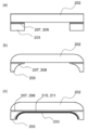
- a bonding apparatus 100 shown in FIG. 1A includes a vacuum vessel 101, a substrate support 104 disposed inside the vacuum vessel 101, and movably supporting a first substrate 102 and a second substrate 103, and a surface A particle beam source 105 as an activation processing means, a metal target 106 for forming a thin film of metal oxide, and a substrate support 104 as a bonding means have a rotating shaft 104A and a pressing means (not shown). It is configured. With this configuration, a metal oxide of good quality is formed on the substrates 102 and 103 in vacuum, and surface activation treatment and substrate bonding (bonding) can be performed without breaking the vacuum. Bond interface can be formed.
- a vacuum pump (not shown) is connected to the vacuum vessel 101, and the degree of vacuum in the vacuum vessel 101 can be maintained at a pressure of 1 ⁇ 10 -5 Pa or less.
- the particle beam source 105 may be rotatable about the rotation axis 105A, and may accelerate the particle group (107) of the mixed gas of argon and oxygen toward the sputtering target 106 to sputter the metal material.
- the particle beam source 105 emits a particle beam 105B of particles having a predetermined kinetic energy toward the surface of the first substrate 102 or the second substrate 103 according to the position of the substrate support 104, and thereby the surface of the substrate surface. It is configured to be able to perform activation processing.
- a mask defining the predetermined regions is disposed on the substrate (not shown).
- the substrate support 104 can be scanned to make the deposition conditions on the first substrate 102 or the second substrate 103 uniform.
- the thickness of the metal oxide layer is determined by the number of scans with respect to the predetermined operating conditions of the particle beam source 105 and the predetermined arrangement positions of the particle beam source 105, the target 106, and the substrates 102 and 103 in the vacuum vessel 101. It may be controlled stepwise.
- glass substrates were used for both the first substrate 102 and the second substrate 103, and more specifically, non-alkali glass (OA10-G manufactured by Nippon Electric Glass Co., Ltd.) of 80 mm square was used.
- the glass substrates 112 and 113 were introduced into the vacuum vessel 101, the atmosphere in the vessel was set to a vacuum atmosphere of 10 -5 Pa or less, and evacuation was continued with the same evacuation capacity until bonding was completed.
- a target 106 is metal aluminum, and a mixed gas of argon gas and oxygen gas is supplied at a flow rate of 80 sccm under conditions of 1.2 kV and 400 mA. It was driven.
- the particle beam 105B of the mixed gas is irradiated to the target 106, and the particle group 107 containing a mixture of aluminum and oxygen is sputtered toward the bonding surface of both glass substrates.
- thin films of aluminum oxides 107 and 108 were formed on the bonding surfaces of the glass substrates 102 and 103 (FIG. 1 (b)). The thickness was about 20 nm.
- the present disclosure is not limited to the above description of the mechanism of sputtering and the state of the sputtered particles 107 from the target 106 to the substrates 102 and 103.
- the particle beam source 105 is rotated about the rotation axis 105A and fixed at a position facing the first substrate 102 or the second substrate 103,
- the surface of the aluminum oxide films 107 and 108 formed on the substrates 102 and 103 is driven at 1.3 kV 400 mV at a supply rate of 70 sccm of argon gas using the same particle beam source 105 to drive the energetic particle beam 105 C Irradiated.
- a mask defining the predetermined area is disposed on the substrate (not shown).
- the substrate support 104 is configured to have, as a bonding means, a rotation shaft 104A provided between portions supporting the first substrate 102 and the second substrate 103. There is.
- the substrate support 104 is configured to be folded so that the first substrate 102 and the second substrate 103 face each other around the rotation axis 104A.
- the first substrate 102 and the second substrate 103 can be brought into contact with each other using a simple configuration, and the same pressure can be applied uniformly over substantially the entire area of each other. it can.
- pressing means for applying a predetermined force is arranged from the outside of the folded substrate support 104 so as to press the first substrate 102 and the second substrate 103 against each other during bonding.
- the surface activation processed aluminum oxide thin films formed on both substrates were brought into contact with each other. After contact, a force of 5 kN was applied perpendicular to the interface for 5 minutes.
- a heating means (not shown) is provided which heats the first substrate 102 and the second substrate 103 at a predetermined temperature within a range not to degrade the material of the substrate and the function of the electronic device during bonding. Good.
- pressing means for applying a predetermined force is arranged from the outside of the folded substrate support 104 so as to press the first substrate 102 and the second substrate 103 against each other during bonding. Good.
- heating means (not shown) which heats at a predetermined temperature within the range that does not degrade the functions of the materials and electronic elements included in the substrates 102 and 103 and the metal oxides 107 and 108 during bonding. Good.
- the light transmittance is a visible light transmittance measured by a commercially available visible light transmittance measuring device. Generally, it refers to the ratio before and after transmission of a light beam in the visible light region or in the wavelength region of about 360 nm to about 760 nm.
- the light transmittance measured for the substrates stacked in a state before the method for forming a laminate is referred to as light transmittance before bonding, and the light transmission measured for the laminate after the method for bonding a substrate is performed.
- the rate is called light transmittance after bonding.
- what divided light transmittance after junction by light transmittance before junction is called light transmittance ratio.
- the light transmittance before bonding was 91.59%.
- the strength of the bonding interface was measured by the blade insertion method.
- a blade (blade) is inserted between two joined substrates to peel off the substrate, and the surface energy is evaluated from the length from the point of the raed tooth to 剝
- the bonding strength is a method used to evaluate the bonding strength of wafer bonding.
- An Ar: O 2 flow ratio of 0% indicates that a thin film of substantially 100% Al is formed. In that case, it is considered that the light transmittance is relatively low because the metal thin film at the substrate bonding interface absorbs visible light.
- the Ar: O 2 flow ratio is increased, the target aluminum is sputtered together with oxygen so that the thin film formed on the substrate interface is a mixture of aluminum and oxygen or an oxide of aluminum metal.
- a thin film of Aluminum oxide is a substance transparent to visible light, such as sapphire or alumina.
- the mixture of aluminum and oxygen formed is considered to partially contain alumina (aluminum oxide).
- the thin film of aluminum oxide may contain a portion of non-stoichiometric composition at atomic level.
- the transmittance of the thin film is increased by increasing the proportion of aluminum oxide having high light transparency in the formed thin film as the Ar: O 2 flow ratio is increased.
- the flow ratio of Ar: O 2 is 5%
- the thin film is substantially made of aluminum oxide or alumina and the oxidation degree approaches saturation.
- the light transmittance almost reaches the saturated state.
- the mechanism of the increase in light transmittance and the saturation with the increase of the Ar: O 2 flow ratio is not limited to the above, and may be another mechanism.
- the bonding strength tends to decrease as the Ar: O 2 flow rate ratio for Al target sputtering increases.
- Aluminum which is a metal
- aluminum oxide which is an oxide. Therefore, it is considered that the bonding strength decreases as the percentage of metal on the thin film surface decreases or as the percentage of oxide on the thin film surface increases.
- the bonding strength is 7.5% or more, the value becomes almost constant. It is considered that this is because the proportion of the oxide on the thin film surface is almost saturated or reaches a certain proportion as the influence on the bonding strength.
- the reason why the Ar: O 2 flow rate ratio becomes almost constant between the light transmittance and the bonding strength is considered to be the difference in that it is not sensitive to the proportion of the oxide in the thin film.
- the Ar: O 2 flow ratio is 5%
- the ratio of the thin film oxide has not reached the limit, and the metallic aluminum component is present to some extent, but it is not It is considered that the influence was not exerted, or the influence was at least negligible in the measurement technique.
- the discussion of the above mechanism is an inference, not the one specified above, but may be another mechanism.
- the bonding strength is also influenced by the surface roughness of the metal oxide film. Generally, when the surface roughness of the metal oxide film is large, the bonding strength is also reduced. Therefore, it can be understood that the absolute value of this experimental result is one actual measurement value, and the tendency is relative.
- Example 2 The polymer substrates were bonded using the method according to the present disclosure.
- a PEN (polyethylene naphthalate) film Teijin Ltd. Theonex ® and a PI (polyimide) film (Kupton & manufactured by DuPont) were used.
- Various films were heated at a temperature of 70 ° C. to 150 ° C. for 1 hour to 4 hours as dehydration treatment before forming the metal oxide film.
- Each PEN, each PI, PEN and a glass substrate, and each PI and a glass substrate were joined.
- An aluminum oxide film was formed on either PEN or PI in the same manner as in Example 1.
- An aluminum oxide film was not formed on the glass substrate.
- the surface activation process similar to Example 1 was performed with respect to the surface bonded, the board
- the light transmittance ratio of the light transmittance after bonding divided by the light transmittance before bonding was 97% or more and was extremely high.
- a substrate laminate can be formed by the substrate bonding method of the present disclosure.
- the present substrate laminate may be a transparent substrate laminate.
- the substrate laminate of the present disclosure comprises a first substrate, a second substrate, and a layer substantially consisting of a metal oxide between the first substrate and the second substrate, which substrate It may be a transparent substrate laminate in which the light transmittance of the laminate is 97% or more of the light transmittance when the first substrate and the second substrate are superimposed.
- the light transmittance of the substrate laminate is 98% or more, 99% or more, 99.1% or more, 99% of the light transmittance when the first substrate and the second substrate are superimposed. 2% or more, 99.3% or more, 99.4% or more, or 99.5% or more.
- the substrate laminate of the present disclosure comprises a first substrate, a second substrate, and a layer substantially consisting of a metal oxide between the first substrate and the second substrate, which substrate
- the transparent substrate laminated body whose light transmittance ratio of a laminated body is 97% or more may be sufficient.
- the light transmittance is 98% or more, 99% or more, 99.1% or more, 99.2% or more, 99.3% or more, 99.4% or more, or 99.5% or more. May be
- the light is taken out from the light emitting element in the laminate compared to the light transmittance from the glass substrate of light extracted from the light emitting element
- the light transmittance of the light from the glass substrate is 97% or more, 98 or more, 99% or more, 99.1% or more, 99.2% or more, 99.3% or more, 99.4% or more, or 99. It may be 5% or more.
- Substrate laminate included in this disclosure the joining strength or interfacial energy, 0.3 J / m 2 or more, 0.4 J / m 2 or more, 0.5 J / m 2 or more, 1 J / m 2 or more, 1. 5 J / m 2 or more, or may be 2J / m 2 or more.
- the bonding strength can be converted to the energy of the bonding interface as described above.
- the bonding strength may be measured as the breaking strength of the bonding interface, or may be the breaking strength of the bonding interface.
- the blade insertion method is easily applied to the case where the bonding substrate is a substrate made of a material which is hard to plastically deform to a certain extent, such as a semiconductor wafer or a glass substrate.
- the bonding strength may be measured by a peel test.
- the breaking strength may be measured by a peel test to evaluate the bonding strength. In the peel method, the bonding strength may be 0.5 N / cm or more.
- the transparent substrate laminate included in the present disclosure does not contain an organic material such as OCA, and is composed only of an inorganic material, so it is applied to an application range or device based on the use of a situation where the organic material is not preferred can do.
- the transparent substrate laminate included in the present disclosure may be used for transparent panels used in space where resistance to radiation such as alpha rays is required.
- the present disclosure includes an optoelectronic device having a transparent substrate laminate, a solar cell, a space solar cell, a radiation resistant solar cell, a radiation resistant optoelectronic device.
- the present disclosure also includes an aerospace device or body such as an aircraft, an artificial satellite, a rocket, a space station, or the like, a window material or window used in construction, a pressure resistant glass, etc. that includes such a transparent substrate laminate.
- the substrate laminate formed by bonding the substrates was further heated at 100 ° C., 150 ° C. or 200 ° C. It was confirmed that the bonding strength after heating generally increases as compared to the bonding strength without heating.
- the atmosphere in the heat treatment may be the air or an inert gas such as nitrogen or argon.
- a metal thin film is formed on the bonding surface of the transparent substrate, the substrate is bonded via the metal thin film, and the substrate is irradiated with a laser by irradiating the metal thin film sandwiched between the substrates.
- Techniques are known for absorbing metals and consequently obtaining relatively transparent substrate laminates.
- metal may not be completely absorbed by the substrate, which may cause problems with light transmission.
- a polymer film provided with an organic EL element or the like is attached to a transparent substrate.
- laser heating is not suitable for relatively low resistance materials and components such as polymer films.
- the method of forming the laminate of the present disclosure is also suitable for the bonding of polymer films because it is not necessary to inject high energy into the bonding interface. Furthermore, it is not necessary to intervene OCA, and a laminate having high transparency, high adhesion and high transparency can be formed.
- the substrates to be bonded may be flat or flat, or non-flat.
- the substrates to be joined may be curved curved glass substrates, and may include tempered glass having curved surfaces.
- the substrate or the laminate to be joined may have an L-shaped cross section, a U-shaped cross section, or an arc shaped cross section. These substrates and laminates may be used in electronic display devices such as smartphones and tablets having a three-dimensional shape and having displays or optical elements on curved surfaces or sides.
- the other substrate to be bonded or the second substrate may be a flexible substrate or may include a flexible substrate.
- the flexible substrate may include an optical element.
- the method of bonding the substrate of the present disclosure can avoid the use of OCA and directly bond a cover glass and a functional film such as a deflection film through a metal oxide film, thereby solving the above-mentioned drawbacks and having high transparency. It becomes possible to form a laminate.
- both of the pair of substrates to be joined are glass substrates, one of the substrates or the first substrate is a glass substrate and the second substrate has a smaller bonding area than the first substrate. It may be a glass substrate.
- the second substrate may be a glass substrate having a frame or frame shape along the edge of the first substrate. The second substrate may also be bonded to part of the edge of the first substrate.
- the first substrate may be a substantially rectangular flat glass substrate, and the second substrate may be bonded along a pair of opposing sides of the first substrate.
- the second substrate may include a plurality of substrates. All glass substrates in the present disclosure may be made of tempered glass or may be a substrate containing tempered glass.
- the method for bonding substrates included in the present disclosure is a bonding in which the first substrate is a glass substrate or a substrate including a glass substrate, and the second substrate is bonded to part or all of the edge of the first substrate. It is a substrate having a surface, and after bonding the first substrate and the second substrate, machining the bonded first substrate and the second substrate to form a curved glass substrate is further performed. May be included.
- the method of bonding substrates included in the present disclosure may include machining the bonded first and second substrates to form a curved surface at least in part thereof. Good.
- This machining may include at least one of grinding and polishing. Machining may be performed in a manner that avoids bending. Since ordinary tempered glass is weak to bending and difficult to bend, there is a problem that the bent tempered glass becomes expensive.
- the above method solves this problem and forms a curved glass substrate or a curved surface-reinforced glass substrate having a desired curved surface shape without bending or deformation processing at high temperature. Can.
- a method of bonding substrates includes forming thin films 207, 208 of a first metal oxide on the bonding surface of the first substrate 202 and the first bonding surface of the second substrate 203; Performing a first activation treatment on the surface of the thin film 207, 208 of the first metal oxide of the bonding surface of the first substrate 202 of the second substrate and the bonding surface of the second substrate 202; Bonding the first substrate 202 and the second substrate 203 by bringing the bonding surface of the first substrate 202 and the first bonding surface of the second substrate 203 into contact with each other through the thin films 207 and 208 Forming second metal oxide thin films 210 and 211 on the second bonding surface of the second substrate 203 and the bonding surface of the third substrate 209, and on the second bonding surface of the second substrate 203 The surface of the second metal oxide thin film 210, 211 on the bonding surface of the three substrates 209 And the second bonding surface of the second substrate 202 and the bonding surface of the third substrate 209
- the bonding method of the substrate may bond the third substrate 209 to the first substrate 202.
- the third substrate 209 may be bonded to the first substrate 202 and the second substrate 203. That is, the bonding surface of the third substrate 209 is brought into contact with the second bonding surface of the third substrate 202 and the second bonding surface of the second substrate 202, and the first substrate 201 and the second Bonding of the second substrate 203 and the third substrate 209 may be included.
- the first substrate 202 and the second substrate 203 may be a transparent substrate, a substrate of tempered glass, or a substrate containing tempered glass.
- the third substrate may be a flexible substrate. As described above, it is difficult to process flat tempered glass, or bent tempered glass is expensive. Therefore, it is possible to create an electronic display device that is cheaper and has a high light extraction efficiency.
- the present disclosure also includes electronic or optoelectronic or optical devices manufactured by methods including any of the substrate bonding methods disclosed in the present application, and generally includes devices.
- the device may include a laminate produced by a method including any of the substrate bonding methods of the present disclosure.
- the device may comprise an organic EL element.
- the device may be a smartphone, a display device, a solar cell, a SAW filter device, or a building material such as a window, pressure resistant glass, and the like.
Abstract
L'invention concerne un procédé pour lier un substrat, lequel procédé comprend : la formation d'un film mince d'un oxyde métallique sur la surface de liaison de l'un ou des deux d'une paire de substrats, au moins l'un des substrats étant un substrat transparent, et le fait d'amener les faces de liaison de la paire de substrats en contact l'une avec l'autre avec le film mince d'oxyde métallique interposé entre celles-ci.
Priority Applications (4)
| Application Number | Priority Date | Filing Date | Title |
|---|---|---|---|
| KR1020207021853A KR20200105868A (ko) | 2017-12-28 | 2018-12-21 | 기판의 접합 방법, 투명기판 적층체 및 기판 적층체를 구비하는 디바이스 |
| US16/958,955 US20210017075A1 (en) | 2017-12-28 | 2018-12-21 | Method for bonding substrate, transparent substrate laminate, and device provided with substrate laminate |
| EP18897427.3A EP3736134A4 (fr) | 2017-12-28 | 2018-12-21 | Procédé pour lier un substrat, stratifié de substrats transparent, et dispositif comportant un stratifié de substrats |
| CN201880087846.XA CN111655490B (zh) | 2017-12-28 | 2018-12-21 | 基板的接合方法、基板层叠体和具备基板层叠体的器件 |
Applications Claiming Priority (2)
| Application Number | Priority Date | Filing Date | Title |
|---|---|---|---|
| JP2017254137A JP7045186B2 (ja) | 2017-12-28 | 2017-12-28 | 基板の接合方法、透明基板積層体及び基板積層体を備えるデバイス |
| JP2017-254137 | 2017-12-28 |
Publications (1)
| Publication Number | Publication Date |
|---|---|
| WO2019131490A1 true WO2019131490A1 (fr) | 2019-07-04 |
Family
ID=67067315
Family Applications (1)
| Application Number | Title | Priority Date | Filing Date |
|---|---|---|---|
| PCT/JP2018/047204 WO2019131490A1 (fr) | 2017-12-28 | 2018-12-21 | Procédé pour lier un substrat, stratifié de substrats transparent, et dispositif comportant un stratifié de substrats |
Country Status (6)
| Country | Link |
|---|---|
| US (1) | US20210017075A1 (fr) |
| EP (1) | EP3736134A4 (fr) |
| JP (1) | JP7045186B2 (fr) |
| KR (1) | KR20200105868A (fr) |
| CN (1) | CN111655490B (fr) |
| WO (1) | WO2019131490A1 (fr) |
Cited By (2)
| Publication number | Priority date | Publication date | Assignee | Title |
|---|---|---|---|---|
| WO2020111015A1 (fr) * | 2018-11-26 | 2020-06-04 | ランテクニカルサービス株式会社 | Procédé de jonction de substrats transparents, et corps stratifié |
| EP4026644A4 (fr) * | 2019-09-05 | 2023-09-27 | Tohoku University | Procédé de liaison chimique et structure assemblée |
Families Citing this family (4)
| Publication number | Priority date | Publication date | Assignee | Title |
|---|---|---|---|---|
| CN112897899B (zh) * | 2021-01-21 | 2022-06-14 | 杭州中科神光科技有限公司 | 一种玻璃组件键合的方法 |
| CN112919815B (zh) * | 2021-01-21 | 2022-06-03 | 杭州中科神光科技有限公司 | 一种玻璃组件键合的方法 |
| US20220336405A1 (en) * | 2021-04-15 | 2022-10-20 | Apple Inc. | Method of Fine Pitch Hybrid Bonding with Dissimilar CTE Wafers and Resulting Structures |
| WO2022242879A1 (fr) * | 2021-05-21 | 2022-11-24 | Applied Materials, Inc. | Appareil et procédé de fabrication d'un film composite |
Citations (9)
| Publication number | Priority date | Publication date | Assignee | Title |
|---|---|---|---|---|
| JP2004337927A (ja) * | 2003-05-15 | 2004-12-02 | Tadatomo Suga | 基板接合方法および基板接合装置 |
| JP2008207221A (ja) * | 2007-02-27 | 2008-09-11 | Takehito Shimazu | 常温接合方法 |
| JP2009199902A (ja) * | 2008-02-21 | 2009-09-03 | Seiko Epson Corp | 有機発光装置および電子機器 |
| WO2013154107A1 (fr) * | 2012-04-10 | 2013-10-17 | ランテクニカルサービス株式会社 | Procédé de liaison de films polymères, procédé de liaison d'un film polymère à un substrat de matière inorganique, stratifié de film polymère, et stratifié de film polymère et substrat de matière inorganique |
| WO2013187500A1 (fr) * | 2012-06-15 | 2013-12-19 | ランテクニカルサービス株式会社 | Procédé de scellement d'un élément électronique et jonction de substrat |
| JP2014123514A (ja) * | 2012-12-21 | 2014-07-03 | Ran Technical Service Kk | 電子素子の封止方法及び封止構造 |
| JP2015111659A (ja) * | 2013-10-28 | 2015-06-18 | 日亜化学工業株式会社 | 発光装置及びその製造方法 |
| JP2015207615A (ja) * | 2014-04-18 | 2015-11-19 | 日亜化学工業株式会社 | 半導体発光装置およびその製造方法 |
| JP2017157611A (ja) * | 2016-02-29 | 2017-09-07 | 日亜化学工業株式会社 | 発光装置及びその製造方法 |
Family Cites Families (5)
| Publication number | Priority date | Publication date | Assignee | Title |
|---|---|---|---|---|
| JP2008094063A (ja) * | 2006-10-16 | 2008-04-24 | Asahi Kasei Chemicals Corp | 金属酸化物積層体 |
| KR20150023312A (ko) * | 2012-05-29 | 2015-03-05 | 아사히 가라스 가부시키가이샤 | 유리 적층체 및 전자 디바이스의 제조 방법 |
| CN102941712B (zh) * | 2012-10-23 | 2015-07-22 | 江南大学 | 一种高分子材料-金属氧化物薄膜复合材料及其制备方法 |
| US9703011B2 (en) * | 2013-05-07 | 2017-07-11 | Corning Incorporated | Scratch-resistant articles with a gradient layer |
| JP6282142B2 (ja) * | 2014-03-03 | 2018-02-21 | 日東電工株式会社 | 赤外線反射基板およびその製造方法 |
-
2017
- 2017-12-28 JP JP2017254137A patent/JP7045186B2/ja active Active
-
2018
- 2018-12-21 CN CN201880087846.XA patent/CN111655490B/zh active Active
- 2018-12-21 WO PCT/JP2018/047204 patent/WO2019131490A1/fr unknown
- 2018-12-21 US US16/958,955 patent/US20210017075A1/en active Pending
- 2018-12-21 EP EP18897427.3A patent/EP3736134A4/fr active Pending
- 2018-12-21 KR KR1020207021853A patent/KR20200105868A/ko active IP Right Grant
Patent Citations (10)
| Publication number | Priority date | Publication date | Assignee | Title |
|---|---|---|---|---|
| JP2004337927A (ja) * | 2003-05-15 | 2004-12-02 | Tadatomo Suga | 基板接合方法および基板接合装置 |
| JP2008207221A (ja) * | 2007-02-27 | 2008-09-11 | Takehito Shimazu | 常温接合方法 |
| JP2009199902A (ja) * | 2008-02-21 | 2009-09-03 | Seiko Epson Corp | 有機発光装置および電子機器 |
| WO2013154107A1 (fr) * | 2012-04-10 | 2013-10-17 | ランテクニカルサービス株式会社 | Procédé de liaison de films polymères, procédé de liaison d'un film polymère à un substrat de matière inorganique, stratifié de film polymère, et stratifié de film polymère et substrat de matière inorganique |
| WO2013187500A1 (fr) * | 2012-06-15 | 2013-12-19 | ランテクニカルサービス株式会社 | Procédé de scellement d'un élément électronique et jonction de substrat |
| JP2015111596A (ja) * | 2012-06-15 | 2015-06-18 | 須賀 唯知 | 電子素子の封止方法及び基板接合体 |
| JP2014123514A (ja) * | 2012-12-21 | 2014-07-03 | Ran Technical Service Kk | 電子素子の封止方法及び封止構造 |
| JP2015111659A (ja) * | 2013-10-28 | 2015-06-18 | 日亜化学工業株式会社 | 発光装置及びその製造方法 |
| JP2015207615A (ja) * | 2014-04-18 | 2015-11-19 | 日亜化学工業株式会社 | 半導体発光装置およびその製造方法 |
| JP2017157611A (ja) * | 2016-02-29 | 2017-09-07 | 日亜化学工業株式会社 | 発光装置及びその製造方法 |
Cited By (2)
| Publication number | Priority date | Publication date | Assignee | Title |
|---|---|---|---|---|
| WO2020111015A1 (fr) * | 2018-11-26 | 2020-06-04 | ランテクニカルサービス株式会社 | Procédé de jonction de substrats transparents, et corps stratifié |
| EP4026644A4 (fr) * | 2019-09-05 | 2023-09-27 | Tohoku University | Procédé de liaison chimique et structure assemblée |
Also Published As
| Publication number | Publication date |
|---|---|
| KR20200105868A (ko) | 2020-09-09 |
| CN111655490A (zh) | 2020-09-11 |
| EP3736134A4 (fr) | 2021-09-15 |
| JP2019119086A (ja) | 2019-07-22 |
| US20210017075A1 (en) | 2021-01-21 |
| CN111655490B (zh) | 2023-06-02 |
| EP3736134A1 (fr) | 2020-11-11 |
| JP7045186B2 (ja) | 2022-03-31 |
Similar Documents
| Publication | Publication Date | Title |
|---|---|---|
| WO2019131490A1 (fr) | Procédé pour lier un substrat, stratifié de substrats transparent, et dispositif comportant un stratifié de substrats | |
| US9962908B2 (en) | Method for bonding polymer film and polymer film, method for bonding polymer film and inorganic material substrate, polymer film laminate, and laminate of polymer film and inorganic material substrate | |
| US9331305B2 (en) | Electronic element sealing method and bonded substrate | |
| EP3240015B1 (fr) | Dispositif à semi-conducteur et procédé de fabrication de dispositif à semi-conducteur | |
| WO2016010106A1 (fr) | Substrat mince, son procédé de fabrication, et procédé de transport de substrat | |
| JP2016115930A (ja) | 電子素子の製造方法、可撓性基板の製造方法、積層基板および電子素子 | |
| JP5033870B2 (ja) | タッチパネル、タッチパネルの製造方法 | |
| JP7287772B2 (ja) | 透明基板の接合方法及び積層体 | |
| JP2017188204A (ja) | 薄型基板およびその製造方法、並びに基板の剥離方法 | |
| JP2000286593A (ja) | 電磁波遮蔽積層体の製造方法 | |
| JP2017016957A (ja) | 基板接合体及びその製造方法 | |
| WO2020116404A1 (fr) | Procédé de scellement de dispositif | |
| JPH07214344A (ja) | 積層接合装置 |
Legal Events
| Date | Code | Title | Description |
|---|---|---|---|
| 121 | Ep: the epo has been informed by wipo that ep was designated in this application |
Ref document number: 18897427 Country of ref document: EP Kind code of ref document: A1 |
|
| NENP | Non-entry into the national phase |
Ref country code: DE |
|
| ENP | Entry into the national phase |
Ref document number: 20207021853 Country of ref document: KR Kind code of ref document: A |
|
| ENP | Entry into the national phase |
Ref document number: 2018897427 Country of ref document: EP Effective date: 20200728 |