WO2019131490A1 - Method for bonding substrate, transparent substrate laminate, and device provided with substrate laminate - Google Patents
Method for bonding substrate, transparent substrate laminate, and device provided with substrate laminate Download PDFInfo
- Publication number
- WO2019131490A1 WO2019131490A1 PCT/JP2018/047204 JP2018047204W WO2019131490A1 WO 2019131490 A1 WO2019131490 A1 WO 2019131490A1 JP 2018047204 W JP2018047204 W JP 2018047204W WO 2019131490 A1 WO2019131490 A1 WO 2019131490A1
- Authority
- WO
- WIPO (PCT)
- Prior art keywords
- substrate
- bonding
- substrates
- metal oxide
- thin film
- Prior art date
Links
Images


Classifications
-
- C—CHEMISTRY; METALLURGY
- C03—GLASS; MINERAL OR SLAG WOOL
- C03C—CHEMICAL COMPOSITION OF GLASSES, GLAZES OR VITREOUS ENAMELS; SURFACE TREATMENT OF GLASS; SURFACE TREATMENT OF FIBRES OR FILAMENTS MADE FROM GLASS, MINERALS OR SLAGS; JOINING GLASS TO GLASS OR OTHER MATERIALS
- C03C27/00—Joining pieces of glass to pieces of other inorganic material; Joining glass to glass other than by fusing
- C03C27/06—Joining glass to glass by processes other than fusing
- C03C27/10—Joining glass to glass by processes other than fusing with the aid of adhesive specially adapted for that purpose
-
- B—PERFORMING OPERATIONS; TRANSPORTING
- B32—LAYERED PRODUCTS
- B32B—LAYERED PRODUCTS, i.e. PRODUCTS BUILT-UP OF STRATA OF FLAT OR NON-FLAT, e.g. CELLULAR OR HONEYCOMB, FORM
- B32B37/00—Methods or apparatus for laminating, e.g. by curing or by ultrasonic bonding
- B32B37/14—Methods or apparatus for laminating, e.g. by curing or by ultrasonic bonding characterised by the properties of the layers
- B32B37/26—Methods or apparatus for laminating, e.g. by curing or by ultrasonic bonding characterised by the properties of the layers with at least one layer which influences the bonding during the lamination process, e.g. release layers or pressure equalising layers
-
- B—PERFORMING OPERATIONS; TRANSPORTING
- B29—WORKING OF PLASTICS; WORKING OF SUBSTANCES IN A PLASTIC STATE IN GENERAL
- B29C—SHAPING OR JOINING OF PLASTICS; SHAPING OF MATERIAL IN A PLASTIC STATE, NOT OTHERWISE PROVIDED FOR; AFTER-TREATMENT OF THE SHAPED PRODUCTS, e.g. REPAIRING
- B29C59/00—Surface shaping of articles, e.g. embossing; Apparatus therefor
- B29C59/14—Surface shaping of articles, e.g. embossing; Apparatus therefor by plasma treatment
-
- B—PERFORMING OPERATIONS; TRANSPORTING
- B32—LAYERED PRODUCTS
- B32B—LAYERED PRODUCTS, i.e. PRODUCTS BUILT-UP OF STRATA OF FLAT OR NON-FLAT, e.g. CELLULAR OR HONEYCOMB, FORM
- B32B17/00—Layered products essentially comprising sheet glass, or glass, slag, or like fibres
- B32B17/06—Layered products essentially comprising sheet glass, or glass, slag, or like fibres comprising glass as the main or only constituent of a layer, next to another layer of a specific material
- B32B17/10—Layered products essentially comprising sheet glass, or glass, slag, or like fibres comprising glass as the main or only constituent of a layer, next to another layer of a specific material of synthetic resin
-
- B—PERFORMING OPERATIONS; TRANSPORTING
- B32—LAYERED PRODUCTS
- B32B—LAYERED PRODUCTS, i.e. PRODUCTS BUILT-UP OF STRATA OF FLAT OR NON-FLAT, e.g. CELLULAR OR HONEYCOMB, FORM
- B32B27/00—Layered products comprising a layer of synthetic resin
- B32B27/06—Layered products comprising a layer of synthetic resin as the main or only constituent of a layer, which is next to another layer of the same or of a different material
- B32B27/08—Layered products comprising a layer of synthetic resin as the main or only constituent of a layer, which is next to another layer of the same or of a different material of synthetic resin
-
- B—PERFORMING OPERATIONS; TRANSPORTING
- B32—LAYERED PRODUCTS
- B32B—LAYERED PRODUCTS, i.e. PRODUCTS BUILT-UP OF STRATA OF FLAT OR NON-FLAT, e.g. CELLULAR OR HONEYCOMB, FORM
- B32B27/00—Layered products comprising a layer of synthetic resin
- B32B27/28—Layered products comprising a layer of synthetic resin comprising synthetic resins not wholly covered by any one of the sub-groups B32B27/30 - B32B27/42
- B32B27/281—Layered products comprising a layer of synthetic resin comprising synthetic resins not wholly covered by any one of the sub-groups B32B27/30 - B32B27/42 comprising polyimides
-
- B—PERFORMING OPERATIONS; TRANSPORTING
- B32—LAYERED PRODUCTS
- B32B—LAYERED PRODUCTS, i.e. PRODUCTS BUILT-UP OF STRATA OF FLAT OR NON-FLAT, e.g. CELLULAR OR HONEYCOMB, FORM
- B32B27/00—Layered products comprising a layer of synthetic resin
- B32B27/32—Layered products comprising a layer of synthetic resin comprising polyolefins
- B32B27/325—Layered products comprising a layer of synthetic resin comprising polyolefins comprising polycycloolefins
-
- B—PERFORMING OPERATIONS; TRANSPORTING
- B32—LAYERED PRODUCTS
- B32B—LAYERED PRODUCTS, i.e. PRODUCTS BUILT-UP OF STRATA OF FLAT OR NON-FLAT, e.g. CELLULAR OR HONEYCOMB, FORM
- B32B27/00—Layered products comprising a layer of synthetic resin
- B32B27/36—Layered products comprising a layer of synthetic resin comprising polyesters
- B32B27/365—Layered products comprising a layer of synthetic resin comprising polyesters comprising polycarbonates
-
- B—PERFORMING OPERATIONS; TRANSPORTING
- B32—LAYERED PRODUCTS
- B32B—LAYERED PRODUCTS, i.e. PRODUCTS BUILT-UP OF STRATA OF FLAT OR NON-FLAT, e.g. CELLULAR OR HONEYCOMB, FORM
- B32B37/00—Methods or apparatus for laminating, e.g. by curing or by ultrasonic bonding
- B32B37/14—Methods or apparatus for laminating, e.g. by curing or by ultrasonic bonding characterised by the properties of the layers
- B32B37/24—Methods or apparatus for laminating, e.g. by curing or by ultrasonic bonding characterised by the properties of the layers with at least one layer not being coherent before laminating, e.g. made up from granular material sprinkled onto a substrate
-
- B—PERFORMING OPERATIONS; TRANSPORTING
- B32—LAYERED PRODUCTS
- B32B—LAYERED PRODUCTS, i.e. PRODUCTS BUILT-UP OF STRATA OF FLAT OR NON-FLAT, e.g. CELLULAR OR HONEYCOMB, FORM
- B32B38/00—Ancillary operations in connection with laminating processes
- B32B38/0008—Electrical discharge treatment, e.g. corona, plasma treatment; wave energy or particle radiation
-
- B—PERFORMING OPERATIONS; TRANSPORTING
- B32—LAYERED PRODUCTS
- B32B—LAYERED PRODUCTS, i.e. PRODUCTS BUILT-UP OF STRATA OF FLAT OR NON-FLAT, e.g. CELLULAR OR HONEYCOMB, FORM
- B32B38/00—Ancillary operations in connection with laminating processes
- B32B38/0036—Heat treatment
-
- B—PERFORMING OPERATIONS; TRANSPORTING
- B32—LAYERED PRODUCTS
- B32B—LAYERED PRODUCTS, i.e. PRODUCTS BUILT-UP OF STRATA OF FLAT OR NON-FLAT, e.g. CELLULAR OR HONEYCOMB, FORM
- B32B7/00—Layered products characterised by the relation between layers; Layered products characterised by the relative orientation of features between layers, or by the relative values of a measurable parameter between layers, i.e. products comprising layers having different physical, chemical or physicochemical properties; Layered products characterised by the interconnection of layers
- B32B7/04—Interconnection of layers
- B32B7/12—Interconnection of layers using interposed adhesives or interposed materials with bonding properties
-
- C—CHEMISTRY; METALLURGY
- C03—GLASS; MINERAL OR SLAG WOOL
- C03C—CHEMICAL COMPOSITION OF GLASSES, GLAZES OR VITREOUS ENAMELS; SURFACE TREATMENT OF GLASS; SURFACE TREATMENT OF FIBRES OR FILAMENTS MADE FROM GLASS, MINERALS OR SLAGS; JOINING GLASS TO GLASS OR OTHER MATERIALS
- C03C17/00—Surface treatment of glass, not in the form of fibres or filaments, by coating
- C03C17/22—Surface treatment of glass, not in the form of fibres or filaments, by coating with other inorganic material
- C03C17/23—Oxides
- C03C17/245—Oxides by deposition from the vapour phase
-
- C—CHEMISTRY; METALLURGY
- C03—GLASS; MINERAL OR SLAG WOOL
- C03C—CHEMICAL COMPOSITION OF GLASSES, GLAZES OR VITREOUS ENAMELS; SURFACE TREATMENT OF GLASS; SURFACE TREATMENT OF FIBRES OR FILAMENTS MADE FROM GLASS, MINERALS OR SLAGS; JOINING GLASS TO GLASS OR OTHER MATERIALS
- C03C27/00—Joining pieces of glass to pieces of other inorganic material; Joining glass to glass other than by fusing
- C03C27/04—Joining glass to metal by means of an interlayer
- C03C27/042—Joining glass to metal by means of an interlayer consisting of a combination of materials selected from glass, glass-ceramic or ceramic material with metals, metal oxides or metal salts
-
- C—CHEMISTRY; METALLURGY
- C03—GLASS; MINERAL OR SLAG WOOL
- C03C—CHEMICAL COMPOSITION OF GLASSES, GLAZES OR VITREOUS ENAMELS; SURFACE TREATMENT OF GLASS; SURFACE TREATMENT OF FIBRES OR FILAMENTS MADE FROM GLASS, MINERALS OR SLAGS; JOINING GLASS TO GLASS OR OTHER MATERIALS
- C03C27/00—Joining pieces of glass to pieces of other inorganic material; Joining glass to glass other than by fusing
- C03C27/06—Joining glass to glass by processes other than fusing
-
- C—CHEMISTRY; METALLURGY
- C23—COATING METALLIC MATERIAL; COATING MATERIAL WITH METALLIC MATERIAL; CHEMICAL SURFACE TREATMENT; DIFFUSION TREATMENT OF METALLIC MATERIAL; COATING BY VACUUM EVAPORATION, BY SPUTTERING, BY ION IMPLANTATION OR BY CHEMICAL VAPOUR DEPOSITION, IN GENERAL; INHIBITING CORROSION OF METALLIC MATERIAL OR INCRUSTATION IN GENERAL
- C23C—COATING METALLIC MATERIAL; COATING MATERIAL WITH METALLIC MATERIAL; SURFACE TREATMENT OF METALLIC MATERIAL BY DIFFUSION INTO THE SURFACE, BY CHEMICAL CONVERSION OR SUBSTITUTION; COATING BY VACUUM EVAPORATION, BY SPUTTERING, BY ION IMPLANTATION OR BY CHEMICAL VAPOUR DEPOSITION, IN GENERAL
- C23C14/00—Coating by vacuum evaporation, by sputtering or by ion implantation of the coating forming material
- C23C14/0021—Reactive sputtering or evaporation
- C23C14/0036—Reactive sputtering
-
- C—CHEMISTRY; METALLURGY
- C23—COATING METALLIC MATERIAL; COATING MATERIAL WITH METALLIC MATERIAL; CHEMICAL SURFACE TREATMENT; DIFFUSION TREATMENT OF METALLIC MATERIAL; COATING BY VACUUM EVAPORATION, BY SPUTTERING, BY ION IMPLANTATION OR BY CHEMICAL VAPOUR DEPOSITION, IN GENERAL; INHIBITING CORROSION OF METALLIC MATERIAL OR INCRUSTATION IN GENERAL
- C23C—COATING METALLIC MATERIAL; COATING MATERIAL WITH METALLIC MATERIAL; SURFACE TREATMENT OF METALLIC MATERIAL BY DIFFUSION INTO THE SURFACE, BY CHEMICAL CONVERSION OR SUBSTITUTION; COATING BY VACUUM EVAPORATION, BY SPUTTERING, BY ION IMPLANTATION OR BY CHEMICAL VAPOUR DEPOSITION, IN GENERAL
- C23C14/00—Coating by vacuum evaporation, by sputtering or by ion implantation of the coating forming material
- C23C14/02—Pretreatment of the material to be coated
- C23C14/021—Cleaning or etching treatments
- C23C14/022—Cleaning or etching treatments by means of bombardment with energetic particles or radiation
-
- C—CHEMISTRY; METALLURGY
- C23—COATING METALLIC MATERIAL; COATING MATERIAL WITH METALLIC MATERIAL; CHEMICAL SURFACE TREATMENT; DIFFUSION TREATMENT OF METALLIC MATERIAL; COATING BY VACUUM EVAPORATION, BY SPUTTERING, BY ION IMPLANTATION OR BY CHEMICAL VAPOUR DEPOSITION, IN GENERAL; INHIBITING CORROSION OF METALLIC MATERIAL OR INCRUSTATION IN GENERAL
- C23C—COATING METALLIC MATERIAL; COATING MATERIAL WITH METALLIC MATERIAL; SURFACE TREATMENT OF METALLIC MATERIAL BY DIFFUSION INTO THE SURFACE, BY CHEMICAL CONVERSION OR SUBSTITUTION; COATING BY VACUUM EVAPORATION, BY SPUTTERING, BY ION IMPLANTATION OR BY CHEMICAL VAPOUR DEPOSITION, IN GENERAL
- C23C14/00—Coating by vacuum evaporation, by sputtering or by ion implantation of the coating forming material
- C23C14/04—Coating on selected surface areas, e.g. using masks
- C23C14/042—Coating on selected surface areas, e.g. using masks using masks
-
- C—CHEMISTRY; METALLURGY
- C23—COATING METALLIC MATERIAL; COATING MATERIAL WITH METALLIC MATERIAL; CHEMICAL SURFACE TREATMENT; DIFFUSION TREATMENT OF METALLIC MATERIAL; COATING BY VACUUM EVAPORATION, BY SPUTTERING, BY ION IMPLANTATION OR BY CHEMICAL VAPOUR DEPOSITION, IN GENERAL; INHIBITING CORROSION OF METALLIC MATERIAL OR INCRUSTATION IN GENERAL
- C23C—COATING METALLIC MATERIAL; COATING MATERIAL WITH METALLIC MATERIAL; SURFACE TREATMENT OF METALLIC MATERIAL BY DIFFUSION INTO THE SURFACE, BY CHEMICAL CONVERSION OR SUBSTITUTION; COATING BY VACUUM EVAPORATION, BY SPUTTERING, BY ION IMPLANTATION OR BY CHEMICAL VAPOUR DEPOSITION, IN GENERAL
- C23C14/00—Coating by vacuum evaporation, by sputtering or by ion implantation of the coating forming material
- C23C14/06—Coating by vacuum evaporation, by sputtering or by ion implantation of the coating forming material characterised by the coating material
- C23C14/08—Oxides
- C23C14/081—Oxides of aluminium, magnesium or beryllium
-
- C—CHEMISTRY; METALLURGY
- C23—COATING METALLIC MATERIAL; COATING MATERIAL WITH METALLIC MATERIAL; CHEMICAL SURFACE TREATMENT; DIFFUSION TREATMENT OF METALLIC MATERIAL; COATING BY VACUUM EVAPORATION, BY SPUTTERING, BY ION IMPLANTATION OR BY CHEMICAL VAPOUR DEPOSITION, IN GENERAL; INHIBITING CORROSION OF METALLIC MATERIAL OR INCRUSTATION IN GENERAL
- C23C—COATING METALLIC MATERIAL; COATING MATERIAL WITH METALLIC MATERIAL; SURFACE TREATMENT OF METALLIC MATERIAL BY DIFFUSION INTO THE SURFACE, BY CHEMICAL CONVERSION OR SUBSTITUTION; COATING BY VACUUM EVAPORATION, BY SPUTTERING, BY ION IMPLANTATION OR BY CHEMICAL VAPOUR DEPOSITION, IN GENERAL
- C23C14/00—Coating by vacuum evaporation, by sputtering or by ion implantation of the coating forming material
- C23C14/22—Coating by vacuum evaporation, by sputtering or by ion implantation of the coating forming material characterised by the process of coating
- C23C14/56—Apparatus specially adapted for continuous coating; Arrangements for maintaining the vacuum, e.g. vacuum locks
-
- C—CHEMISTRY; METALLURGY
- C23—COATING METALLIC MATERIAL; COATING MATERIAL WITH METALLIC MATERIAL; CHEMICAL SURFACE TREATMENT; DIFFUSION TREATMENT OF METALLIC MATERIAL; COATING BY VACUUM EVAPORATION, BY SPUTTERING, BY ION IMPLANTATION OR BY CHEMICAL VAPOUR DEPOSITION, IN GENERAL; INHIBITING CORROSION OF METALLIC MATERIAL OR INCRUSTATION IN GENERAL
- C23C—COATING METALLIC MATERIAL; COATING MATERIAL WITH METALLIC MATERIAL; SURFACE TREATMENT OF METALLIC MATERIAL BY DIFFUSION INTO THE SURFACE, BY CHEMICAL CONVERSION OR SUBSTITUTION; COATING BY VACUUM EVAPORATION, BY SPUTTERING, BY ION IMPLANTATION OR BY CHEMICAL VAPOUR DEPOSITION, IN GENERAL
- C23C14/00—Coating by vacuum evaporation, by sputtering or by ion implantation of the coating forming material
- C23C14/58—After-treatment
- C23C14/5826—Treatment with charged particles
- C23C14/5833—Ion beam bombardment
-
- C—CHEMISTRY; METALLURGY
- C23—COATING METALLIC MATERIAL; COATING MATERIAL WITH METALLIC MATERIAL; CHEMICAL SURFACE TREATMENT; DIFFUSION TREATMENT OF METALLIC MATERIAL; COATING BY VACUUM EVAPORATION, BY SPUTTERING, BY ION IMPLANTATION OR BY CHEMICAL VAPOUR DEPOSITION, IN GENERAL; INHIBITING CORROSION OF METALLIC MATERIAL OR INCRUSTATION IN GENERAL
- C23C—COATING METALLIC MATERIAL; COATING MATERIAL WITH METALLIC MATERIAL; SURFACE TREATMENT OF METALLIC MATERIAL BY DIFFUSION INTO THE SURFACE, BY CHEMICAL CONVERSION OR SUBSTITUTION; COATING BY VACUUM EVAPORATION, BY SPUTTERING, BY ION IMPLANTATION OR BY CHEMICAL VAPOUR DEPOSITION, IN GENERAL
- C23C16/00—Chemical coating by decomposition of gaseous compounds, without leaving reaction products of surface material in the coating, i.e. chemical vapour deposition [CVD] processes
- C23C16/44—Chemical coating by decomposition of gaseous compounds, without leaving reaction products of surface material in the coating, i.e. chemical vapour deposition [CVD] processes characterised by the method of coating
- C23C16/455—Chemical coating by decomposition of gaseous compounds, without leaving reaction products of surface material in the coating, i.e. chemical vapour deposition [CVD] processes characterised by the method of coating characterised by the method used for introducing gases into reaction chamber or for modifying gas flows in reaction chamber
-
- H—ELECTRICITY
- H01—ELECTRIC ELEMENTS
- H01L—SEMICONDUCTOR DEVICES NOT COVERED BY CLASS H10
- H01L24/00—Arrangements for connecting or disconnecting semiconductor or solid-state bodies; Methods or apparatus related thereto
- H01L24/80—Methods for connecting semiconductor or other solid state bodies using means for bonding being attached to, or being formed on, the surface to be connected
- H01L24/83—Methods for connecting semiconductor or other solid state bodies using means for bonding being attached to, or being formed on, the surface to be connected using a layer connector
-
- H—ELECTRICITY
- H05—ELECTRIC TECHNIQUES NOT OTHERWISE PROVIDED FOR
- H05B—ELECTRIC HEATING; ELECTRIC LIGHT SOURCES NOT OTHERWISE PROVIDED FOR; CIRCUIT ARRANGEMENTS FOR ELECTRIC LIGHT SOURCES, IN GENERAL
- H05B33/00—Electroluminescent light sources
- H05B33/02—Details
-
- H—ELECTRICITY
- H05—ELECTRIC TECHNIQUES NOT OTHERWISE PROVIDED FOR
- H05B—ELECTRIC HEATING; ELECTRIC LIGHT SOURCES NOT OTHERWISE PROVIDED FOR; CIRCUIT ARRANGEMENTS FOR ELECTRIC LIGHT SOURCES, IN GENERAL
- H05B33/00—Electroluminescent light sources
- H05B33/02—Details
- H05B33/04—Sealing arrangements, e.g. against humidity
-
- H—ELECTRICITY
- H10—SEMICONDUCTOR DEVICES; ELECTRIC SOLID-STATE DEVICES NOT OTHERWISE PROVIDED FOR
- H10K—ORGANIC ELECTRIC SOLID-STATE DEVICES
- H10K50/00—Organic light-emitting devices
-
- H—ELECTRICITY
- H10—SEMICONDUCTOR DEVICES; ELECTRIC SOLID-STATE DEVICES NOT OTHERWISE PROVIDED FOR
- H10K—ORGANIC ELECTRIC SOLID-STATE DEVICES
- H10K71/00—Manufacture or treatment specially adapted for the organic devices covered by this subclass
- H10K71/50—Forming devices by joining two substrates together, e.g. lamination techniques
-
- H—ELECTRICITY
- H10—SEMICONDUCTOR DEVICES; ELECTRIC SOLID-STATE DEVICES NOT OTHERWISE PROVIDED FOR
- H10K—ORGANIC ELECTRIC SOLID-STATE DEVICES
- H10K77/00—Constructional details of devices covered by this subclass and not covered by groups H10K10/80, H10K30/80, H10K50/80 or H10K59/80
- H10K77/10—Substrates, e.g. flexible substrates
-
- B—PERFORMING OPERATIONS; TRANSPORTING
- B29—WORKING OF PLASTICS; WORKING OF SUBSTANCES IN A PLASTIC STATE IN GENERAL
- B29C—SHAPING OR JOINING OF PLASTICS; SHAPING OF MATERIAL IN A PLASTIC STATE, NOT OTHERWISE PROVIDED FOR; AFTER-TREATMENT OF THE SHAPED PRODUCTS, e.g. REPAIRING
- B29C65/00—Joining or sealing of preformed parts, e.g. welding of plastics materials; Apparatus therefor
- B29C65/02—Joining or sealing of preformed parts, e.g. welding of plastics materials; Apparatus therefor by heating, with or without pressure
-
- B—PERFORMING OPERATIONS; TRANSPORTING
- B29—WORKING OF PLASTICS; WORKING OF SUBSTANCES IN A PLASTIC STATE IN GENERAL
- B29C—SHAPING OR JOINING OF PLASTICS; SHAPING OF MATERIAL IN A PLASTIC STATE, NOT OTHERWISE PROVIDED FOR; AFTER-TREATMENT OF THE SHAPED PRODUCTS, e.g. REPAIRING
- B29C65/00—Joining or sealing of preformed parts, e.g. welding of plastics materials; Apparatus therefor
- B29C65/82—Testing the joint
- B29C65/8207—Testing the joint by mechanical methods
- B29C65/8223—Peel tests
-
- B—PERFORMING OPERATIONS; TRANSPORTING
- B29—WORKING OF PLASTICS; WORKING OF SUBSTANCES IN A PLASTIC STATE IN GENERAL
- B29C—SHAPING OR JOINING OF PLASTICS; SHAPING OF MATERIAL IN A PLASTIC STATE, NOT OTHERWISE PROVIDED FOR; AFTER-TREATMENT OF THE SHAPED PRODUCTS, e.g. REPAIRING
- B29C66/00—General aspects of processes or apparatus for joining preformed parts
- B29C66/001—Joining in special atmospheres
- B29C66/0012—Joining in special atmospheres characterised by the type of environment
- B29C66/0014—Gaseous environments
- B29C66/00141—Protective gases
-
- B—PERFORMING OPERATIONS; TRANSPORTING
- B29—WORKING OF PLASTICS; WORKING OF SUBSTANCES IN A PLASTIC STATE IN GENERAL
- B29C—SHAPING OR JOINING OF PLASTICS; SHAPING OF MATERIAL IN A PLASTIC STATE, NOT OTHERWISE PROVIDED FOR; AFTER-TREATMENT OF THE SHAPED PRODUCTS, e.g. REPAIRING
- B29C66/00—General aspects of processes or apparatus for joining preformed parts
- B29C66/001—Joining in special atmospheres
- B29C66/0012—Joining in special atmospheres characterised by the type of environment
- B29C66/0014—Gaseous environments
- B29C66/00143—Active gases
-
- B—PERFORMING OPERATIONS; TRANSPORTING
- B29—WORKING OF PLASTICS; WORKING OF SUBSTANCES IN A PLASTIC STATE IN GENERAL
- B29C—SHAPING OR JOINING OF PLASTICS; SHAPING OF MATERIAL IN A PLASTIC STATE, NOT OTHERWISE PROVIDED FOR; AFTER-TREATMENT OF THE SHAPED PRODUCTS, e.g. REPAIRING
- B29C66/00—General aspects of processes or apparatus for joining preformed parts
- B29C66/001—Joining in special atmospheres
- B29C66/0012—Joining in special atmospheres characterised by the type of environment
- B29C66/0014—Gaseous environments
- B29C66/00145—Vacuum, e.g. partial vacuum
-
- B—PERFORMING OPERATIONS; TRANSPORTING
- B29—WORKING OF PLASTICS; WORKING OF SUBSTANCES IN A PLASTIC STATE IN GENERAL
- B29C—SHAPING OR JOINING OF PLASTICS; SHAPING OF MATERIAL IN A PLASTIC STATE, NOT OTHERWISE PROVIDED FOR; AFTER-TREATMENT OF THE SHAPED PRODUCTS, e.g. REPAIRING
- B29C66/00—General aspects of processes or apparatus for joining preformed parts
- B29C66/01—General aspects dealing with the joint area or with the area to be joined
- B29C66/02—Preparation of the material, in the area to be joined, prior to joining or welding
- B29C66/024—Thermal pre-treatments
- B29C66/0242—Heating, or preheating, e.g. drying
-
- B—PERFORMING OPERATIONS; TRANSPORTING
- B29—WORKING OF PLASTICS; WORKING OF SUBSTANCES IN A PLASTIC STATE IN GENERAL
- B29C—SHAPING OR JOINING OF PLASTICS; SHAPING OF MATERIAL IN A PLASTIC STATE, NOT OTHERWISE PROVIDED FOR; AFTER-TREATMENT OF THE SHAPED PRODUCTS, e.g. REPAIRING
- B29C66/00—General aspects of processes or apparatus for joining preformed parts
- B29C66/01—General aspects dealing with the joint area or with the area to be joined
- B29C66/02—Preparation of the material, in the area to be joined, prior to joining or welding
- B29C66/028—Non-mechanical surface pre-treatments, i.e. by flame treatment, electric discharge treatment, plasma treatment, wave energy or particle radiation
-
- B—PERFORMING OPERATIONS; TRANSPORTING
- B29—WORKING OF PLASTICS; WORKING OF SUBSTANCES IN A PLASTIC STATE IN GENERAL
- B29C—SHAPING OR JOINING OF PLASTICS; SHAPING OF MATERIAL IN A PLASTIC STATE, NOT OTHERWISE PROVIDED FOR; AFTER-TREATMENT OF THE SHAPED PRODUCTS, e.g. REPAIRING
- B29C66/00—General aspects of processes or apparatus for joining preformed parts
- B29C66/01—General aspects dealing with the joint area or with the area to be joined
- B29C66/03—After-treatments in the joint area
- B29C66/034—Thermal after-treatments
-
- B—PERFORMING OPERATIONS; TRANSPORTING
- B29—WORKING OF PLASTICS; WORKING OF SUBSTANCES IN A PLASTIC STATE IN GENERAL
- B29C—SHAPING OR JOINING OF PLASTICS; SHAPING OF MATERIAL IN A PLASTIC STATE, NOT OTHERWISE PROVIDED FOR; AFTER-TREATMENT OF THE SHAPED PRODUCTS, e.g. REPAIRING
- B29C66/00—General aspects of processes or apparatus for joining preformed parts
- B29C66/01—General aspects dealing with the joint area or with the area to be joined
- B29C66/05—Particular design of joint configurations
- B29C66/10—Particular design of joint configurations particular design of the joint cross-sections
- B29C66/11—Joint cross-sections comprising a single joint-segment, i.e. one of the parts to be joined comprising a single joint-segment in the joint cross-section
- B29C66/112—Single lapped joints
- B29C66/1122—Single lap to lap joints, i.e. overlap joints
-
- B—PERFORMING OPERATIONS; TRANSPORTING
- B29—WORKING OF PLASTICS; WORKING OF SUBSTANCES IN A PLASTIC STATE IN GENERAL
- B29C—SHAPING OR JOINING OF PLASTICS; SHAPING OF MATERIAL IN A PLASTIC STATE, NOT OTHERWISE PROVIDED FOR; AFTER-TREATMENT OF THE SHAPED PRODUCTS, e.g. REPAIRING
- B29C66/00—General aspects of processes or apparatus for joining preformed parts
- B29C66/40—General aspects of joining substantially flat articles, e.g. plates, sheets or web-like materials; Making flat seams in tubular or hollow articles; Joining single elements to substantially flat surfaces
- B29C66/41—Joining substantially flat articles ; Making flat seams in tubular or hollow articles
- B29C66/45—Joining of substantially the whole surface of the articles
-
- B—PERFORMING OPERATIONS; TRANSPORTING
- B29—WORKING OF PLASTICS; WORKING OF SUBSTANCES IN A PLASTIC STATE IN GENERAL
- B29C—SHAPING OR JOINING OF PLASTICS; SHAPING OF MATERIAL IN A PLASTIC STATE, NOT OTHERWISE PROVIDED FOR; AFTER-TREATMENT OF THE SHAPED PRODUCTS, e.g. REPAIRING
- B29C66/00—General aspects of processes or apparatus for joining preformed parts
- B29C66/50—General aspects of joining tubular articles; General aspects of joining long products, i.e. bars or profiled elements; General aspects of joining single elements to tubular articles, hollow articles or bars; General aspects of joining several hollow-preforms to form hollow or tubular articles
- B29C66/51—Joining tubular articles, profiled elements or bars; Joining single elements to tubular articles, hollow articles or bars; Joining several hollow-preforms to form hollow or tubular articles
- B29C66/53—Joining single elements to tubular articles, hollow articles or bars
- B29C66/532—Joining single elements to the wall of tubular articles, hollow articles or bars
- B29C66/5326—Joining single elements to the wall of tubular articles, hollow articles or bars said single elements being substantially flat
-
- B—PERFORMING OPERATIONS; TRANSPORTING
- B29—WORKING OF PLASTICS; WORKING OF SUBSTANCES IN A PLASTIC STATE IN GENERAL
- B29C—SHAPING OR JOINING OF PLASTICS; SHAPING OF MATERIAL IN A PLASTIC STATE, NOT OTHERWISE PROVIDED FOR; AFTER-TREATMENT OF THE SHAPED PRODUCTS, e.g. REPAIRING
- B29C66/00—General aspects of processes or apparatus for joining preformed parts
- B29C66/70—General aspects of processes or apparatus for joining preformed parts characterised by the composition, physical properties or the structure of the material of the parts to be joined; Joining with non-plastics material
- B29C66/71—General aspects of processes or apparatus for joining preformed parts characterised by the composition, physical properties or the structure of the material of the parts to be joined; Joining with non-plastics material characterised by the composition of the plastics material of the parts to be joined
-
- B—PERFORMING OPERATIONS; TRANSPORTING
- B29—WORKING OF PLASTICS; WORKING OF SUBSTANCES IN A PLASTIC STATE IN GENERAL
- B29C—SHAPING OR JOINING OF PLASTICS; SHAPING OF MATERIAL IN A PLASTIC STATE, NOT OTHERWISE PROVIDED FOR; AFTER-TREATMENT OF THE SHAPED PRODUCTS, e.g. REPAIRING
- B29C66/00—General aspects of processes or apparatus for joining preformed parts
- B29C66/70—General aspects of processes or apparatus for joining preformed parts characterised by the composition, physical properties or the structure of the material of the parts to be joined; Joining with non-plastics material
- B29C66/73—General aspects of processes or apparatus for joining preformed parts characterised by the composition, physical properties or the structure of the material of the parts to be joined; Joining with non-plastics material characterised by the intensive physical properties of the material of the parts to be joined, by the optical properties of the material of the parts to be joined, by the extensive physical properties of the parts to be joined, by the state of the material of the parts to be joined or by the material of the parts to be joined being a thermoplastic or a thermoset
- B29C66/733—General aspects of processes or apparatus for joining preformed parts characterised by the composition, physical properties or the structure of the material of the parts to be joined; Joining with non-plastics material characterised by the intensive physical properties of the material of the parts to be joined, by the optical properties of the material of the parts to be joined, by the extensive physical properties of the parts to be joined, by the state of the material of the parts to be joined or by the material of the parts to be joined being a thermoplastic or a thermoset characterised by the optical properties of the material of the parts to be joined, e.g. fluorescence, phosphorescence
- B29C66/7336—General aspects of processes or apparatus for joining preformed parts characterised by the composition, physical properties or the structure of the material of the parts to be joined; Joining with non-plastics material characterised by the intensive physical properties of the material of the parts to be joined, by the optical properties of the material of the parts to be joined, by the extensive physical properties of the parts to be joined, by the state of the material of the parts to be joined or by the material of the parts to be joined being a thermoplastic or a thermoset characterised by the optical properties of the material of the parts to be joined, e.g. fluorescence, phosphorescence at least one of the parts to be joined being opaque, transparent or translucent to visible light
- B29C66/73365—General aspects of processes or apparatus for joining preformed parts characterised by the composition, physical properties or the structure of the material of the parts to be joined; Joining with non-plastics material characterised by the intensive physical properties of the material of the parts to be joined, by the optical properties of the material of the parts to be joined, by the extensive physical properties of the parts to be joined, by the state of the material of the parts to be joined or by the material of the parts to be joined being a thermoplastic or a thermoset characterised by the optical properties of the material of the parts to be joined, e.g. fluorescence, phosphorescence at least one of the parts to be joined being opaque, transparent or translucent to visible light at least one of the parts to be joined being transparent or translucent to visible light
- B29C66/73366—General aspects of processes or apparatus for joining preformed parts characterised by the composition, physical properties or the structure of the material of the parts to be joined; Joining with non-plastics material characterised by the intensive physical properties of the material of the parts to be joined, by the optical properties of the material of the parts to be joined, by the extensive physical properties of the parts to be joined, by the state of the material of the parts to be joined or by the material of the parts to be joined being a thermoplastic or a thermoset characterised by the optical properties of the material of the parts to be joined, e.g. fluorescence, phosphorescence at least one of the parts to be joined being opaque, transparent or translucent to visible light at least one of the parts to be joined being transparent or translucent to visible light both parts to be joined being transparent or translucent to visible light
-
- B—PERFORMING OPERATIONS; TRANSPORTING
- B29—WORKING OF PLASTICS; WORKING OF SUBSTANCES IN A PLASTIC STATE IN GENERAL
- B29C—SHAPING OR JOINING OF PLASTICS; SHAPING OF MATERIAL IN A PLASTIC STATE, NOT OTHERWISE PROVIDED FOR; AFTER-TREATMENT OF THE SHAPED PRODUCTS, e.g. REPAIRING
- B29C66/00—General aspects of processes or apparatus for joining preformed parts
- B29C66/70—General aspects of processes or apparatus for joining preformed parts characterised by the composition, physical properties or the structure of the material of the parts to be joined; Joining with non-plastics material
- B29C66/74—Joining plastics material to non-plastics material
- B29C66/746—Joining plastics material to non-plastics material to inorganic materials not provided for in groups B29C66/742 - B29C66/744
- B29C66/7465—Glass
-
- B—PERFORMING OPERATIONS; TRANSPORTING
- B29—WORKING OF PLASTICS; WORKING OF SUBSTANCES IN A PLASTIC STATE IN GENERAL
- B29C—SHAPING OR JOINING OF PLASTICS; SHAPING OF MATERIAL IN A PLASTIC STATE, NOT OTHERWISE PROVIDED FOR; AFTER-TREATMENT OF THE SHAPED PRODUCTS, e.g. REPAIRING
- B29C66/00—General aspects of processes or apparatus for joining preformed parts
- B29C66/80—General aspects of machine operations or constructions and parts thereof
- B29C66/83—General aspects of machine operations or constructions and parts thereof characterised by the movement of the joining or pressing tools
- B29C66/832—Reciprocating joining or pressing tools
- B29C66/8324—Joining or pressing tools pivoting around one axis
- B29C66/83241—Joining or pressing tools pivoting around one axis cooperating pivoting tools
-
- B—PERFORMING OPERATIONS; TRANSPORTING
- B29—WORKING OF PLASTICS; WORKING OF SUBSTANCES IN A PLASTIC STATE IN GENERAL
- B29C—SHAPING OR JOINING OF PLASTICS; SHAPING OF MATERIAL IN A PLASTIC STATE, NOT OTHERWISE PROVIDED FOR; AFTER-TREATMENT OF THE SHAPED PRODUCTS, e.g. REPAIRING
- B29C66/00—General aspects of processes or apparatus for joining preformed parts
- B29C66/90—Measuring or controlling the joining process
- B29C66/91—Measuring or controlling the joining process by measuring or controlling the temperature, the heat or the thermal flux
- B29C66/919—Measuring or controlling the joining process by measuring or controlling the temperature, the heat or the thermal flux characterised by specific temperature, heat or thermal flux values or ranges
-
- B—PERFORMING OPERATIONS; TRANSPORTING
- B29—WORKING OF PLASTICS; WORKING OF SUBSTANCES IN A PLASTIC STATE IN GENERAL
- B29C—SHAPING OR JOINING OF PLASTICS; SHAPING OF MATERIAL IN A PLASTIC STATE, NOT OTHERWISE PROVIDED FOR; AFTER-TREATMENT OF THE SHAPED PRODUCTS, e.g. REPAIRING
- B29C66/00—General aspects of processes or apparatus for joining preformed parts
- B29C66/90—Measuring or controlling the joining process
- B29C66/92—Measuring or controlling the joining process by measuring or controlling the pressure, the force, the mechanical power or the displacement of the joining tools
- B29C66/929—Measuring or controlling the joining process by measuring or controlling the pressure, the force, the mechanical power or the displacement of the joining tools characterized by specific pressure, force, mechanical power or displacement values or ranges
-
- B—PERFORMING OPERATIONS; TRANSPORTING
- B29—WORKING OF PLASTICS; WORKING OF SUBSTANCES IN A PLASTIC STATE IN GENERAL
- B29C—SHAPING OR JOINING OF PLASTICS; SHAPING OF MATERIAL IN A PLASTIC STATE, NOT OTHERWISE PROVIDED FOR; AFTER-TREATMENT OF THE SHAPED PRODUCTS, e.g. REPAIRING
- B29C66/00—General aspects of processes or apparatus for joining preformed parts
- B29C66/90—Measuring or controlling the joining process
- B29C66/94—Measuring or controlling the joining process by measuring or controlling the time
- B29C66/949—Measuring or controlling the joining process by measuring or controlling the time characterised by specific time values or ranges
-
- B—PERFORMING OPERATIONS; TRANSPORTING
- B32—LAYERED PRODUCTS
- B32B—LAYERED PRODUCTS, i.e. PRODUCTS BUILT-UP OF STRATA OF FLAT OR NON-FLAT, e.g. CELLULAR OR HONEYCOMB, FORM
- B32B37/00—Methods or apparatus for laminating, e.g. by curing or by ultrasonic bonding
- B32B37/14—Methods or apparatus for laminating, e.g. by curing or by ultrasonic bonding characterised by the properties of the layers
- B32B37/24—Methods or apparatus for laminating, e.g. by curing or by ultrasonic bonding characterised by the properties of the layers with at least one layer not being coherent before laminating, e.g. made up from granular material sprinkled onto a substrate
- B32B2037/246—Vapour deposition
-
- B—PERFORMING OPERATIONS; TRANSPORTING
- B32—LAYERED PRODUCTS
- B32B—LAYERED PRODUCTS, i.e. PRODUCTS BUILT-UP OF STRATA OF FLAT OR NON-FLAT, e.g. CELLULAR OR HONEYCOMB, FORM
- B32B2255/00—Coating on the layer surface
- B32B2255/10—Coating on the layer surface on synthetic resin layer or on natural or synthetic rubber layer
-
- B—PERFORMING OPERATIONS; TRANSPORTING
- B32—LAYERED PRODUCTS
- B32B—LAYERED PRODUCTS, i.e. PRODUCTS BUILT-UP OF STRATA OF FLAT OR NON-FLAT, e.g. CELLULAR OR HONEYCOMB, FORM
- B32B2255/00—Coating on the layer surface
- B32B2255/20—Inorganic coating
-
- B—PERFORMING OPERATIONS; TRANSPORTING
- B32—LAYERED PRODUCTS
- B32B—LAYERED PRODUCTS, i.e. PRODUCTS BUILT-UP OF STRATA OF FLAT OR NON-FLAT, e.g. CELLULAR OR HONEYCOMB, FORM
- B32B2307/00—Properties of the layers or laminate
- B32B2307/40—Properties of the layers or laminate having particular optical properties
- B32B2307/412—Transparent
-
- B—PERFORMING OPERATIONS; TRANSPORTING
- B32—LAYERED PRODUCTS
- B32B—LAYERED PRODUCTS, i.e. PRODUCTS BUILT-UP OF STRATA OF FLAT OR NON-FLAT, e.g. CELLULAR OR HONEYCOMB, FORM
- B32B2309/00—Parameters for the laminating or treatment process; Apparatus details
- B32B2309/02—Temperature
-
- B—PERFORMING OPERATIONS; TRANSPORTING
- B32—LAYERED PRODUCTS
- B32B—LAYERED PRODUCTS, i.e. PRODUCTS BUILT-UP OF STRATA OF FLAT OR NON-FLAT, e.g. CELLULAR OR HONEYCOMB, FORM
- B32B2309/00—Parameters for the laminating or treatment process; Apparatus details
- B32B2309/60—In a particular environment
- B32B2309/68—Vacuum
-
- B—PERFORMING OPERATIONS; TRANSPORTING
- B32—LAYERED PRODUCTS
- B32B—LAYERED PRODUCTS, i.e. PRODUCTS BUILT-UP OF STRATA OF FLAT OR NON-FLAT, e.g. CELLULAR OR HONEYCOMB, FORM
- B32B2310/00—Treatment by energy or chemical effects
- B32B2310/08—Treatment by energy or chemical effects by wave energy or particle radiation
- B32B2310/0875—Treatment by energy or chemical effects by wave energy or particle radiation using particle radiation
-
- B—PERFORMING OPERATIONS; TRANSPORTING
- B32—LAYERED PRODUCTS
- B32B—LAYERED PRODUCTS, i.e. PRODUCTS BUILT-UP OF STRATA OF FLAT OR NON-FLAT, e.g. CELLULAR OR HONEYCOMB, FORM
- B32B2311/00—Metals, their alloys or their compounds
-
- B—PERFORMING OPERATIONS; TRANSPORTING
- B32—LAYERED PRODUCTS
- B32B—LAYERED PRODUCTS, i.e. PRODUCTS BUILT-UP OF STRATA OF FLAT OR NON-FLAT, e.g. CELLULAR OR HONEYCOMB, FORM
- B32B2315/00—Other materials containing non-metallic inorganic compounds not provided for in groups B32B2311/00 - B32B2313/04
- B32B2315/08—Glass
-
- B—PERFORMING OPERATIONS; TRANSPORTING
- B32—LAYERED PRODUCTS
- B32B—LAYERED PRODUCTS, i.e. PRODUCTS BUILT-UP OF STRATA OF FLAT OR NON-FLAT, e.g. CELLULAR OR HONEYCOMB, FORM
- B32B2419/00—Buildings or parts thereof
-
- B—PERFORMING OPERATIONS; TRANSPORTING
- B32—LAYERED PRODUCTS
- B32B—LAYERED PRODUCTS, i.e. PRODUCTS BUILT-UP OF STRATA OF FLAT OR NON-FLAT, e.g. CELLULAR OR HONEYCOMB, FORM
- B32B2457/00—Electrical equipment
- B32B2457/12—Photovoltaic modules
-
- B—PERFORMING OPERATIONS; TRANSPORTING
- B32—LAYERED PRODUCTS
- B32B—LAYERED PRODUCTS, i.e. PRODUCTS BUILT-UP OF STRATA OF FLAT OR NON-FLAT, e.g. CELLULAR OR HONEYCOMB, FORM
- B32B2457/00—Electrical equipment
- B32B2457/20—Displays, e.g. liquid crystal displays, plasma displays
- B32B2457/206—Organic displays, e.g. OLED
-
- C—CHEMISTRY; METALLURGY
- C03—GLASS; MINERAL OR SLAG WOOL
- C03C—CHEMICAL COMPOSITION OF GLASSES, GLAZES OR VITREOUS ENAMELS; SURFACE TREATMENT OF GLASS; SURFACE TREATMENT OF FIBRES OR FILAMENTS MADE FROM GLASS, MINERALS OR SLAGS; JOINING GLASS TO GLASS OR OTHER MATERIALS
- C03C2217/00—Coatings on glass
- C03C2217/20—Materials for coating a single layer on glass
- C03C2217/21—Oxides
- C03C2217/214—Al2O3
-
- C—CHEMISTRY; METALLURGY
- C03—GLASS; MINERAL OR SLAG WOOL
- C03C—CHEMICAL COMPOSITION OF GLASSES, GLAZES OR VITREOUS ENAMELS; SURFACE TREATMENT OF GLASS; SURFACE TREATMENT OF FIBRES OR FILAMENTS MADE FROM GLASS, MINERALS OR SLAGS; JOINING GLASS TO GLASS OR OTHER MATERIALS
- C03C2218/00—Methods for coating glass
- C03C2218/10—Deposition methods
- C03C2218/15—Deposition methods from the vapour phase
- C03C2218/152—Deposition methods from the vapour phase by cvd
- C03C2218/1525—Deposition methods from the vapour phase by cvd by atmospheric CVD
-
- C—CHEMISTRY; METALLURGY
- C03—GLASS; MINERAL OR SLAG WOOL
- C03C—CHEMICAL COMPOSITION OF GLASSES, GLAZES OR VITREOUS ENAMELS; SURFACE TREATMENT OF GLASS; SURFACE TREATMENT OF FIBRES OR FILAMENTS MADE FROM GLASS, MINERALS OR SLAGS; JOINING GLASS TO GLASS OR OTHER MATERIALS
- C03C2218/00—Methods for coating glass
- C03C2218/10—Deposition methods
- C03C2218/15—Deposition methods from the vapour phase
- C03C2218/154—Deposition methods from the vapour phase by sputtering
-
- C—CHEMISTRY; METALLURGY
- C03—GLASS; MINERAL OR SLAG WOOL
- C03C—CHEMICAL COMPOSITION OF GLASSES, GLAZES OR VITREOUS ENAMELS; SURFACE TREATMENT OF GLASS; SURFACE TREATMENT OF FIBRES OR FILAMENTS MADE FROM GLASS, MINERALS OR SLAGS; JOINING GLASS TO GLASS OR OTHER MATERIALS
- C03C2218/00—Methods for coating glass
- C03C2218/30—Aspects of methods for coating glass not covered above
- C03C2218/32—After-treatment
-
- C—CHEMISTRY; METALLURGY
- C23—COATING METALLIC MATERIAL; COATING MATERIAL WITH METALLIC MATERIAL; CHEMICAL SURFACE TREATMENT; DIFFUSION TREATMENT OF METALLIC MATERIAL; COATING BY VACUUM EVAPORATION, BY SPUTTERING, BY ION IMPLANTATION OR BY CHEMICAL VAPOUR DEPOSITION, IN GENERAL; INHIBITING CORROSION OF METALLIC MATERIAL OR INCRUSTATION IN GENERAL
- C23C—COATING METALLIC MATERIAL; COATING MATERIAL WITH METALLIC MATERIAL; SURFACE TREATMENT OF METALLIC MATERIAL BY DIFFUSION INTO THE SURFACE, BY CHEMICAL CONVERSION OR SUBSTITUTION; COATING BY VACUUM EVAPORATION, BY SPUTTERING, BY ION IMPLANTATION OR BY CHEMICAL VAPOUR DEPOSITION, IN GENERAL
- C23C14/00—Coating by vacuum evaporation, by sputtering or by ion implantation of the coating forming material
- C23C14/22—Coating by vacuum evaporation, by sputtering or by ion implantation of the coating forming material characterised by the process of coating
- C23C14/34—Sputtering
- C23C14/46—Sputtering by ion beam produced by an external ion source
-
- C—CHEMISTRY; METALLURGY
- C23—COATING METALLIC MATERIAL; COATING MATERIAL WITH METALLIC MATERIAL; CHEMICAL SURFACE TREATMENT; DIFFUSION TREATMENT OF METALLIC MATERIAL; COATING BY VACUUM EVAPORATION, BY SPUTTERING, BY ION IMPLANTATION OR BY CHEMICAL VAPOUR DEPOSITION, IN GENERAL; INHIBITING CORROSION OF METALLIC MATERIAL OR INCRUSTATION IN GENERAL
- C23C—COATING METALLIC MATERIAL; COATING MATERIAL WITH METALLIC MATERIAL; SURFACE TREATMENT OF METALLIC MATERIAL BY DIFFUSION INTO THE SURFACE, BY CHEMICAL CONVERSION OR SUBSTITUTION; COATING BY VACUUM EVAPORATION, BY SPUTTERING, BY ION IMPLANTATION OR BY CHEMICAL VAPOUR DEPOSITION, IN GENERAL
- C23C16/00—Chemical coating by decomposition of gaseous compounds, without leaving reaction products of surface material in the coating, i.e. chemical vapour deposition [CVD] processes
- C23C16/44—Chemical coating by decomposition of gaseous compounds, without leaving reaction products of surface material in the coating, i.e. chemical vapour deposition [CVD] processes characterised by the method of coating
- C23C16/455—Chemical coating by decomposition of gaseous compounds, without leaving reaction products of surface material in the coating, i.e. chemical vapour deposition [CVD] processes characterised by the method of coating characterised by the method used for introducing gases into reaction chamber or for modifying gas flows in reaction chamber
- C23C16/45523—Pulsed gas flow or change of composition over time
- C23C16/45525—Atomic layer deposition [ALD]
-
- H—ELECTRICITY
- H01—ELECTRIC ELEMENTS
- H01L—SEMICONDUCTOR DEVICES NOT COVERED BY CLASS H10
- H01L2224/00—Indexing scheme for arrangements for connecting or disconnecting semiconductor or solid-state bodies and methods related thereto as covered by H01L24/00
- H01L2224/80—Methods for connecting semiconductor or other solid state bodies using means for bonding being attached to, or being formed on, the surface to be connected
- H01L2224/83—Methods for connecting semiconductor or other solid state bodies using means for bonding being attached to, or being formed on, the surface to be connected using a layer connector
- H01L2224/83009—Pre-treatment of the layer connector or the bonding area
- H01L2224/83048—Thermal treatments, e.g. annealing, controlled pre-heating or pre-cooling
-
- H—ELECTRICITY
- H01—ELECTRIC ELEMENTS
- H01L—SEMICONDUCTOR DEVICES NOT COVERED BY CLASS H10
- H01L2224/00—Indexing scheme for arrangements for connecting or disconnecting semiconductor or solid-state bodies and methods related thereto as covered by H01L24/00
- H01L2224/80—Methods for connecting semiconductor or other solid state bodies using means for bonding being attached to, or being formed on, the surface to be connected
- H01L2224/83—Methods for connecting semiconductor or other solid state bodies using means for bonding being attached to, or being formed on, the surface to be connected using a layer connector
- H01L2224/83053—Bonding environment
- H01L2224/8309—Vacuum
-
- H—ELECTRICITY
- H01—ELECTRIC ELEMENTS
- H01L—SEMICONDUCTOR DEVICES NOT COVERED BY CLASS H10
- H01L2224/00—Indexing scheme for arrangements for connecting or disconnecting semiconductor or solid-state bodies and methods related thereto as covered by H01L24/00
- H01L2224/80—Methods for connecting semiconductor or other solid state bodies using means for bonding being attached to, or being formed on, the surface to be connected
- H01L2224/83—Methods for connecting semiconductor or other solid state bodies using means for bonding being attached to, or being formed on, the surface to be connected using a layer connector
- H01L2224/83909—Post-treatment of the layer connector or bonding area
- H01L2224/83948—Thermal treatments, e.g. annealing, controlled cooling
-
- Y—GENERAL TAGGING OF NEW TECHNOLOGICAL DEVELOPMENTS; GENERAL TAGGING OF CROSS-SECTIONAL TECHNOLOGIES SPANNING OVER SEVERAL SECTIONS OF THE IPC; TECHNICAL SUBJECTS COVERED BY FORMER USPC CROSS-REFERENCE ART COLLECTIONS [XRACs] AND DIGESTS
- Y02—TECHNOLOGIES OR APPLICATIONS FOR MITIGATION OR ADAPTATION AGAINST CLIMATE CHANGE
- Y02E—REDUCTION OF GREENHOUSE GAS [GHG] EMISSIONS, RELATED TO ENERGY GENERATION, TRANSMISSION OR DISTRIBUTION
- Y02E10/00—Energy generation through renewable energy sources
- Y02E10/50—Photovoltaic [PV] energy
- Y02E10/549—Organic PV cells
Definitions
- the present disclosure relates to a method of bonding substrates. More specifically, the present invention relates to a method of forming a laminate of transparent substrates so as to substantially enjoy the light transmittance of the laminate substrate itself.
- a bonding method of a substrate there is known a method of activating and bonding the surface of a substrate by irradiation with energy particles.
- One such method is cold bonding.
- Substrate bonding techniques using such surface activation processes are currently used in a wide variety of applications.
- it may be used in laminate formation which is not suitable or desired for high temperature processes, in whole or in part of the bonding process.
- it may be used for joining substrates of different materials, or joining substrates of materials in which atomic diffusion is unlikely to occur except under high temperature.
- the present disclosure relates to a method of bonding a substrate, which comprises forming a thin film of a metal oxide on the bonding surface of one or both of a pair of substrates, at least one of which is a transparent substrate; And interposing the bonding surfaces of the substrates in contact with each other.
- an optoelectronic device represented by a display (display element) as an example of a device using a transparent substrate
- a light emitting element is often attached to glass as a component for taking out the light.
- both are pasted via an adhesive film.
- an organic electroluminescence (hereinafter also referred to as "organic EL”) device is obtained by attaching a polymer-covered organic EL element to a protective glass. It is configured. Also in the flexible organic EL, the organic EL element is covered with a polymer, and a polarizing plate or the like is also made of a polymer.
- OCA optically transparent pressure-sensitive adhesive sheet
- the glass is formed using an adhesive formed of an organic material.
- the adhesive is considered to be one cause of the reduction of the light transmittance.
- an organic material is formed by application as an adhesive, air bubbles are easily generated at the bonding interface, which affects the quality of the bonding interface.
- the method of bonding substrates included in the present disclosure includes forming a thin film of a metal oxide on the bonding surface of one or both of a pair of substrates, at least one of which is a transparent substrate, and forming a thin film of metal oxide And bringing the bonding surfaces of the pair of substrates into contact with each other.
- the metal oxide is transparent to visible light, and the metal oxide formed by, for example, sputtering is relatively strong in bonding power. Therefore, it has both permeability and adhesion.
- Transparent substrate refers to a substrate having high transmittance of light including visible light.
- the visible light transmittance may be 90% or more.
- the “transparent substrate” may be a substrate based on or containing SiO 2 -containing glass, tempered glass, polymer or the like. The method of bonding the substrates included in the present disclosure has many advantages, but one advantage is also the substrate comprising SiO 2 which has not been able to be bonded without loss of transparency or significant loss. It is possible to bond while maintaining high light transmittance.
- One or both of the substrates bonded to the transparent substrate may be a transparent substrate.
- the substrates to be bonded may be a pair of substrates, or a pair of transparent substrates, one of which may be a transparent substrate and the other of which may be a semitransparent or opaque substrate.
- Both of the pair of substrates to be bonded may be glass substrates or polymer substrates.
- One of the pair of substrates to be bonded may be a glass substrate, and the other may be a polymer substrate.
- the polymer substrate may be a substrate substantially made of a polymer material. At least one bonding surface of the substrates to be bonded may be substantially made of a polymer material.
- the method of bonding the substrates may include providing a substrate used for bonding or a transparent substrate and another substrate, and may also include providing a pair of substrates at least one of which is a transparent substrate. Good.
- the substrates to be bonded may be a substrate mainly made of a polymer material, or a polymer substrate.
- the polymer material substrate may be a plastic substrate or a flexible substrate.
- the polymeric material may be or is limited to PEN (polyethylene naphthalate), PET (polyethylene terephthalate), other polyester materials, PI (polyimide), COP (cycloolefin polymer), PC (precarbonate), etc. It may be other polymer or plastic material.
- the substrate may include POL (deflection filter).
- the substrate may be substantially made of a polymeric material, may contain a polymeric material, and may be made of a polymeric material and another material or member.
- the polymer substrate may be a transparent substrate.
- the substrates to be bonded may be circular or rectangular, or in the form of a band (tape).
- One of the substrates to be bonded may include an optical element.
- the optical element may be a light emitting element, a light receiving element or the like, and may include other light, photoelectric or electronic elements, circuits, and materials.
- the substrate to be bonded may include the layer of the optical element, or may be formed including the layer of the optical element and the layer of the polymer.
- the substrate may be configured to include a layer including an optical element or an optical element layer, and a layer including a polymer material or a polymer layer.
- One of the substrates to be bonded may be configured to include an optical element layer including an optical element and a polymer layer including a polymer material covering the optical element layer.
- the surface of the polymer layer may be a bonding surface.
- the optical element when the optical element is a light emitting element, all substrates and layers through which light emitted from the light emitting element to the outside of the product passes are preferably transparent, for example, the optical element is a light receiving element In some cases, all substrates and layers through which light incident from the outside of the product passes before reaching the light receiving element are preferably transparent.
- transparent means that a practically sufficient amount of light emitted from the light emitting element is extracted to the outside, or the light incident from the outside is practically used. It is said to be transparent to the extent that a sufficient amount of light is detected by the light receiving element.
- the light transmittance of the transparent substrate laminate formed by bonding has a sufficient light transmittance in the application of the final product.
- the light transmittance after bonding is 90% or more of the light transmittance (hereinafter referred to as “light transmittance before bonding”) with respect to all of a plurality of substrates obtained by superposing the substrates in the state before bonding.
- the light transmittance after bonding may be 95% or more of the light transmittance before bonding.
- the light transmittance after bonding may be 97% or more, 98% or more, or 99% or more of the light transmittance before bonding.
- the metal of the metal oxide is a typical metal alkali metal: Li, Na, K, Rb, Cs or alkaline earth metal: Ca, Sr, Ba, Ra, magnesium group element: Be, Mg, Zn, Cd, Hg, Aluminum group elements: Al, Ga, In, rare earth elements: Y, La, Ce, Pr, Nd, Sm, Eu, tin group elements: Ti, Zr, Sn, Hf, Pb, Th, iron group elements: Fe, Co , Ni, earth element: V, Nb, Ta, chromium group element: Cr, Mo, W, U, manganese group element: Mn, Re, noble metal: Cu, Ag, Au, platinum group element: Ru, Rh, Pd , Os, Ir, Pt may be selected.
- the metal may consist of one kind of metal, may contain a plurality of metals, or may be an alloy.
- the metal may be Si or so-called metallic silicon.
- the metal may be a metal other than silicon.
- the metal oxide may in one embodiment be a metal oxide of stoichiometric composition, in another embodiment it may be non-stoichiometric composition, for example the amount of metal is oxygen It may be more or less than it.
- the metal oxide may be a mixture of metal and oxygen, and the bond of metal and oxygen may be different from that of the metal oxide of stoichiometric composition, and may include different ones.
- Forming a thin film of metal oxide on the bonding surface of the substrate may be performed by plasma CVD, sputtering, vapor deposition, ALD (atomic layer deposition), RIE (reactive ion etching), and RIE.
- plasma CVD chemical vapor deposition
- ALD atomic layer deposition
- RIE reactive ion etching
- RIE reactive ion etching
- Forming a thin film of metal oxide on the bonding surface of a substrate may be performed by sputtering, or may be performed by a method or process including sputtering.
- the sputtering method may be ion beam sputtering or ion beam assisted sputtering.
- the metal oxide formed by the ion beam sputtering method has relatively low crystallinity, relatively many crystal defects, relatively many surfaces exposed by atomic bell, and has many so-called dangling bonds. It is thought that Therefore, it is considered that the activity is relatively high, the surface is in an activated state, and bonding is facilitated. However, this physical consideration is inference, and the present disclosure is not limited to this mechanism.
- forming a thin film of metal oxide on the bonding surface of the substrate may be performed by ion beam assisted sputtering.
- the method may include forming a metal oxide on a target substrate by a sputtering method in which a metal is used as a target and a mixed gas substantially including an inert gas and oxygen is used.
- the sputtering method may be performed with a target gas of metal and a mixed gas substantially consisting of nitrogen gas and oxygen.
- forming a thin film of metal oxide on the bonding surface of the substrate targets the metal, sputters substantially toward the bonding surface with an inert gas, and is directed to the bonding surface from the other direction It may include delivering oxygen gas.
- the inert gas may be a noble gas.
- the noble gas may be any one of helium (He), neon (Ne), argon (Ar), krypton (Kr), xenon (Xe) and radon (Rn), and a plurality of these may be selected. It may be a mixed gas.
- the inert gas may in particular be argon (Ar).
- the metal used for the sputtering target may be aluminum (Al).
- a thin film of aluminum oxide such as Al 2 O 3 can be formed by sputtering film formation using a mixed gas of a rare gas such as argon and an oxygen gas on an aluminum target.
- the oxide of aluminum in the thin film may be a stoichiometric composition Al 2 O 3 , a non-stoichiometric composition, or a mixture thereof.
- the bonding form of aluminum and oxygen may be different from that of Al 2 O 3 of the stoichiometric composition, or may be different.
- Forming a thin film of metal oxide on the bonding surface of the substrate may include forming a metal oxide on a target substrate by targeting the metal oxide and sputtering the target.
- the metal oxide as the target may be aluminum oxide (Al 2 O 3 ).
- the gas used for sputtering may be a noble gas or nitrogen gas, or a mixture thereof, and may be a gas containing noble gas or nitrogen gas and another gas.
- the mixed gas used for sputtering may substantially consist of argon gas and oxygen gas.
- the flow rate of oxygen gas contained in the mixed gas is substantially 3%, 4%, 5%, 6%, 7%, 8%, 9% or 10% of the flow rate or total flow rate of the mixed gas Or a value greater than or equal to any value.
- the mixed gas may contain other argon gas, and may contain a noble gas other than argon gas. If the mixed gas contains a gas different from argon gas, or if the sputtering characteristics substantially or significantly differ due to the influence of equipment or environment, an appropriate oxygen gas flow rate may be selected. . For example, if the sputtering rate of the rare gas is smaller than when only argon gas is used, the flow rate ratio of oxygen may be smaller than 5%, and may be, for example, 4% or 3% or less. Conversely, for example, if the sputtering rate of the rare gas is larger than when only argon gas is used, the flow rate ratio of oxygen may be larger than 5%, and may be, for example, 6% or 7% or more.
- the substrate to be bonded may be a glass substrate and a glass substrate, a glass substrate and a polymer material (polymer) substrate, and a polymer substrate and a polymer substrate.
- a metal oxide film may be formed on either or both.
- bonding a bonding surface of glass and polymer when forming a metal oxide film on either one, a metal oxide film may be formed on the polymer, and in many cases the bonding strength can be improved.
- the thickness of the metal oxide film to be formed may be about 0.1 nm to 10 nm, 0.1 nm, 0.2 nm, 0.3 nm, 0.4 nm, 0.5 nm, 1 nm, 2 nm, 3 nm, 4 nm, The value may be 5 nm, 6 nm, 7 nm, 8 nm, 9 nm or more or more.
- the thickness of the metal oxide film to be formed may be 10 nm or less, or may be 9 nm, 8 nm, 7 nm, 6 nm, 5 nm, 4 nm, 3 nm, 2 nm or less or less than the value of 1 nm.
- the thickness of the metal oxide layer in the substrate laminate formed by bonding may be about 0.1 nm to 20 nm.
- the surface activation treatment may include irradiating the energetic particles against the surface of the metal oxide.
- Energetic particles are generated by accelerating ions or neutral atoms or mixtures thereof of the gas particles or atoms used with a particle beam source such as an ion beam source or a fast atom beam (FAB) source. It is also good. Irradiation of energetic particles may be performed using a plasma source.
- a particle beam source such as an ion beam source or a fast atom beam (FAB) source. It is also good. Irradiation of energetic particles may be performed using a plasma source.
- the particle beam source can be used to provide the particles with a predetermined kinetic energy.
- the particle beam source operates in a vacuum, for example at a pressure of 1 ⁇ 10 -5 Pa (pascal) or less. Substances removed from the surface of the metal area are efficiently exhausted out of the atmosphere by the operation of the vacuum pump to draw a relatively high vacuum. This can inhibit the adhesion of undesired substances to the exposed nascent surface.
- the particle beam source can apply a relatively high acceleration voltage so that high kinetic energy can be applied to the particles. Therefore, it is considered that removal of the surface layer and activation of the new surface can be performed efficiently.
- a fast atom beam source As a neutral atom beam source, a fast atom beam source (FAB, Fast Atom Beam) can be used.
- a fast atom beam source (FAB) typically generates a plasma of gas and applies an electric field to the plasma to extract positive ions of ionized particles from the plasma and pass them through the electron cloud for neutrality.
- the power supplied to the fast atom beam source (FAB) may be set to 1.5 kV (kilovolt), 15 mA (milliampere), or 0.1 It may be set to a value between and 500 W (watts).
- the fast atom beam source FAB
- the high speed atom beam of argon (Ar) is irradiated for about 2 minutes, the oxides, contaminants, etc.
- the (surface layer) can be removed to expose the nascent surface.
- a cold cathode ion source can be used as the ion beam source.
- the ion beam source may be a line-type cold cathode ion beam source.
- a linear particle beam source is a particle beam source having a line-shaped (linear) or elongated particle beam radiation port, and a particle beam can be emitted from the radiation port in a line-shaped (linear) manner.
- the length of the radiation port is preferably greater than the diameter of the substrate onto which the particle beam is irradiated. In the case where the substrate is not circular, the length of the radiation port is preferably larger than the largest dimension in the direction in which the radiation port of the substrate moved relative to the particle beam source extends.
- the particle beam emitted from the linear particle beam source illuminates a linear region or an elongated region on the substrate at a certain time during the surface activation process. Then, while the particle beam is emitted from the line-type particle beam source toward the substrate, the substrate support is scanned in the direction perpendicular to the direction in which the radiation port extends. As a result, the irradiation area of the linear particle beam passes over all the junctions of the substrate. Once the line type particle beam source has passed over the substrate, the entire substrate is substantially uniformly illuminated by the particle beam and surface activated.
- a line-type particle beam source is suitable for irradiating the surface of a relatively large substrate with a particle beam relatively uniformly. Also, the line-type particle beam source can irradiate the particle beam relatively uniformly, corresponding to various shapes of the substrate.
- the energy particles may be or may be a mixed gas substantially consisting of a rare gas and an oxygen gas, or may contain other gases.
- oxygen may be depleted from the metal near the surface of the metal oxide.
- the transmittance of light such as visible light may decrease due to the relatively increase in the amount of metal. It is speculated that this may be due to absorption in the region relatively rich in this metal. Therefore, it is considered that the energy particle beam irradiated to the bonding surface can contain oxygen so that this oxygen can be bonded to the metal oxide surface, and oxygen deficiency can be avoided or reduced. It is believed that this makes it possible to obtain sufficient light transmittance of the bonded transparent substrate laminate.
- the energetic particles may be a noble gas or may contain a noble gas.
- the noble gas may be argon or another noble gas.
- the energetic particles may be neutral atoms or ions, may be radical species, or may be a particle group in which they are mixed.
- “Surface activation” is a treatment or step performed on a surface that is not substantially bonded or joined when brought into contact without contacting it, such that the surfaces after such treatment are brought into contact with each other It means a treatment or the like that provides a desired or substantially effective binding.
- the laminate formed by bonding the substrate after the surface activation treatment may or may not be subjected to heating or light treatment as it is.
- the removal rate of the surface layer may vary. Therefore, it is necessary to adjust each condition including the processing time of the surface activation process. For example, the presence of oxygen and carbon contained in the surface layer is confirmed using surface analysis methods such as Auger Electron Spectroscopy (AES) and X-ray Photo Electron Spectroscopy (XPS). A time that can not be used or a longer time may be adopted as a processing time of the surface activation process.
- AES Auger Electron Spectroscopy
- XPS X-ray Photo Electron Spectroscopy
- Bonding may involve bringing the bonding surfaces of the substrates into contact with one another via a thin film of surface activated metal oxide.
- a force may be applied to the substrate from the side opposite to the bonding surface of the substrate or from a surface other than the bonding surface.
- a force perpendicular to the bonding surface may be applied from the outside of the substrate.
- the pressurization may apply a force to be substantially even across the contacted interface.
- pressure may be applied at different times to different sides of the contacted interface.
- the strength of the force upon pressurization may be constant or variable with time.
- the pressurization may be performed at different timings with respect to each part of the bonding surface.
- the bonding surface may be sequentially pressed by sliding the pressing device with respect to the substrate in contact.
- the pressing device may have a roller-shaped pressing unit.
- the substrate in the method of bonding a substrate included in the present disclosure, from forming a metal oxide layer on a bonding surface on a substrate to bringing a pair of substrates into contact or bonding is consistently performed in vacuum or low. It may be performed in an atmosphere under pressure, or may be performed without breaking a vacuum or low pressure atmosphere. The atmosphere in vacuum or under low pressure may be an atmosphere having a pressure of 10 ⁇ 16 Pa or less.
- the substrate may be temporarily removed from vacuum after the formation of the metal oxide layer, in which case a dummy substrate is temporarily bonded to the bonding surface to avoid exposure of the bonding surface to the atmosphere. After being returned to the vacuum again, the dummy substrate may be removed to bring the bonding surfaces into contact in vacuum.
- the atmosphere in vacuum or under low pressure may include this.
- adhesion of unnecessary substances to the bonding surface, adsorption, oxidation or hydroxylation of the bonding surface can be avoided, surface activation can be efficiently performed, and the activated surface activity Can be maintained or suppressed as much as possible, and the occurrence of non-joining portions can be avoided or reduced.
- the bonding method of the substrate included in the present disclosure may further include heating the laminate after bonding.
- the heating temperature may be 100 ° C., 200 ° C., 100 ° C. or more, or 210 ° C., 220 ° C. or less.
- the temperature of heating may be above or above the temperature of 100.degree. C. or 150.degree.
- the heating temperature may be below or below the temperature of 400 ° C., 300 ° C., 250 ° C., 225 ° C., 220 ° C., 210 ° C., 200 ° C., or 150 ° C.
- the temperature of heating may be substantially 100 ° C, 150 ° C, 200 ° C.
- the heating may be performed simultaneously for the entire substrate or may be performed for each part of the substrate.
- Forming a metal oxide layer on the bonding surface, performing activation treatment, bonding a pair of substrates is performed substantially at a bonding interface temperature of 100 ° C. or 200 ° C. or lower, or intentionally heated It may be performed avoiding the processing.
- the bonding method of the substrate included in the present disclosure may further include irradiating the bonding surface of the substrate with energy particles before film formation. By activating the bonding surface of the substrate by the irradiation of the energetic particles, bonding strength between the bonding surface and the thin film formed thereon can be increased.
- Example 1 The glass substrate was joined using the method according to the present disclosure, and the light transmittance and the joint strength were evaluated.
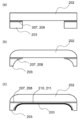
- a bonding apparatus 100 shown in FIG. 1A includes a vacuum vessel 101, a substrate support 104 disposed inside the vacuum vessel 101, and movably supporting a first substrate 102 and a second substrate 103, and a surface A particle beam source 105 as an activation processing means, a metal target 106 for forming a thin film of metal oxide, and a substrate support 104 as a bonding means have a rotating shaft 104A and a pressing means (not shown). It is configured. With this configuration, a metal oxide of good quality is formed on the substrates 102 and 103 in vacuum, and surface activation treatment and substrate bonding (bonding) can be performed without breaking the vacuum. Bond interface can be formed.
- a vacuum pump (not shown) is connected to the vacuum vessel 101, and the degree of vacuum in the vacuum vessel 101 can be maintained at a pressure of 1 ⁇ 10 -5 Pa or less.
- the particle beam source 105 may be rotatable about the rotation axis 105A, and may accelerate the particle group (107) of the mixed gas of argon and oxygen toward the sputtering target 106 to sputter the metal material.
- the particle beam source 105 emits a particle beam 105B of particles having a predetermined kinetic energy toward the surface of the first substrate 102 or the second substrate 103 according to the position of the substrate support 104, and thereby the surface of the substrate surface. It is configured to be able to perform activation processing.
- a mask defining the predetermined regions is disposed on the substrate (not shown).
- the substrate support 104 can be scanned to make the deposition conditions on the first substrate 102 or the second substrate 103 uniform.
- the thickness of the metal oxide layer is determined by the number of scans with respect to the predetermined operating conditions of the particle beam source 105 and the predetermined arrangement positions of the particle beam source 105, the target 106, and the substrates 102 and 103 in the vacuum vessel 101. It may be controlled stepwise.
- glass substrates were used for both the first substrate 102 and the second substrate 103, and more specifically, non-alkali glass (OA10-G manufactured by Nippon Electric Glass Co., Ltd.) of 80 mm square was used.
- the glass substrates 112 and 113 were introduced into the vacuum vessel 101, the atmosphere in the vessel was set to a vacuum atmosphere of 10 -5 Pa or less, and evacuation was continued with the same evacuation capacity until bonding was completed.
- a target 106 is metal aluminum, and a mixed gas of argon gas and oxygen gas is supplied at a flow rate of 80 sccm under conditions of 1.2 kV and 400 mA. It was driven.
- the particle beam 105B of the mixed gas is irradiated to the target 106, and the particle group 107 containing a mixture of aluminum and oxygen is sputtered toward the bonding surface of both glass substrates.
- thin films of aluminum oxides 107 and 108 were formed on the bonding surfaces of the glass substrates 102 and 103 (FIG. 1 (b)). The thickness was about 20 nm.
- the present disclosure is not limited to the above description of the mechanism of sputtering and the state of the sputtered particles 107 from the target 106 to the substrates 102 and 103.
- the particle beam source 105 is rotated about the rotation axis 105A and fixed at a position facing the first substrate 102 or the second substrate 103,
- the surface of the aluminum oxide films 107 and 108 formed on the substrates 102 and 103 is driven at 1.3 kV 400 mV at a supply rate of 70 sccm of argon gas using the same particle beam source 105 to drive the energetic particle beam 105 C Irradiated.
- a mask defining the predetermined area is disposed on the substrate (not shown).
- the substrate support 104 is configured to have, as a bonding means, a rotation shaft 104A provided between portions supporting the first substrate 102 and the second substrate 103. There is.
- the substrate support 104 is configured to be folded so that the first substrate 102 and the second substrate 103 face each other around the rotation axis 104A.
- the first substrate 102 and the second substrate 103 can be brought into contact with each other using a simple configuration, and the same pressure can be applied uniformly over substantially the entire area of each other. it can.
- pressing means for applying a predetermined force is arranged from the outside of the folded substrate support 104 so as to press the first substrate 102 and the second substrate 103 against each other during bonding.
- the surface activation processed aluminum oxide thin films formed on both substrates were brought into contact with each other. After contact, a force of 5 kN was applied perpendicular to the interface for 5 minutes.
- a heating means (not shown) is provided which heats the first substrate 102 and the second substrate 103 at a predetermined temperature within a range not to degrade the material of the substrate and the function of the electronic device during bonding. Good.
- pressing means for applying a predetermined force is arranged from the outside of the folded substrate support 104 so as to press the first substrate 102 and the second substrate 103 against each other during bonding. Good.
- heating means (not shown) which heats at a predetermined temperature within the range that does not degrade the functions of the materials and electronic elements included in the substrates 102 and 103 and the metal oxides 107 and 108 during bonding. Good.
- the light transmittance is a visible light transmittance measured by a commercially available visible light transmittance measuring device. Generally, it refers to the ratio before and after transmission of a light beam in the visible light region or in the wavelength region of about 360 nm to about 760 nm.
- the light transmittance measured for the substrates stacked in a state before the method for forming a laminate is referred to as light transmittance before bonding, and the light transmission measured for the laminate after the method for bonding a substrate is performed.
- the rate is called light transmittance after bonding.
- what divided light transmittance after junction by light transmittance before junction is called light transmittance ratio.
- the light transmittance before bonding was 91.59%.
- the strength of the bonding interface was measured by the blade insertion method.
- a blade (blade) is inserted between two joined substrates to peel off the substrate, and the surface energy is evaluated from the length from the point of the raed tooth to 剝
- the bonding strength is a method used to evaluate the bonding strength of wafer bonding.
- An Ar: O 2 flow ratio of 0% indicates that a thin film of substantially 100% Al is formed. In that case, it is considered that the light transmittance is relatively low because the metal thin film at the substrate bonding interface absorbs visible light.
- the Ar: O 2 flow ratio is increased, the target aluminum is sputtered together with oxygen so that the thin film formed on the substrate interface is a mixture of aluminum and oxygen or an oxide of aluminum metal.
- a thin film of Aluminum oxide is a substance transparent to visible light, such as sapphire or alumina.
- the mixture of aluminum and oxygen formed is considered to partially contain alumina (aluminum oxide).
- the thin film of aluminum oxide may contain a portion of non-stoichiometric composition at atomic level.
- the transmittance of the thin film is increased by increasing the proportion of aluminum oxide having high light transparency in the formed thin film as the Ar: O 2 flow ratio is increased.
- the flow ratio of Ar: O 2 is 5%
- the thin film is substantially made of aluminum oxide or alumina and the oxidation degree approaches saturation.
- the light transmittance almost reaches the saturated state.
- the mechanism of the increase in light transmittance and the saturation with the increase of the Ar: O 2 flow ratio is not limited to the above, and may be another mechanism.
- the bonding strength tends to decrease as the Ar: O 2 flow rate ratio for Al target sputtering increases.
- Aluminum which is a metal
- aluminum oxide which is an oxide. Therefore, it is considered that the bonding strength decreases as the percentage of metal on the thin film surface decreases or as the percentage of oxide on the thin film surface increases.
- the bonding strength is 7.5% or more, the value becomes almost constant. It is considered that this is because the proportion of the oxide on the thin film surface is almost saturated or reaches a certain proportion as the influence on the bonding strength.
- the reason why the Ar: O 2 flow rate ratio becomes almost constant between the light transmittance and the bonding strength is considered to be the difference in that it is not sensitive to the proportion of the oxide in the thin film.
- the Ar: O 2 flow ratio is 5%
- the ratio of the thin film oxide has not reached the limit, and the metallic aluminum component is present to some extent, but it is not It is considered that the influence was not exerted, or the influence was at least negligible in the measurement technique.
- the discussion of the above mechanism is an inference, not the one specified above, but may be another mechanism.
- the bonding strength is also influenced by the surface roughness of the metal oxide film. Generally, when the surface roughness of the metal oxide film is large, the bonding strength is also reduced. Therefore, it can be understood that the absolute value of this experimental result is one actual measurement value, and the tendency is relative.
- Example 2 The polymer substrates were bonded using the method according to the present disclosure.
- a PEN (polyethylene naphthalate) film Teijin Ltd. Theonex ® and a PI (polyimide) film (Kupton & manufactured by DuPont) were used.
- Various films were heated at a temperature of 70 ° C. to 150 ° C. for 1 hour to 4 hours as dehydration treatment before forming the metal oxide film.
- Each PEN, each PI, PEN and a glass substrate, and each PI and a glass substrate were joined.
- An aluminum oxide film was formed on either PEN or PI in the same manner as in Example 1.
- An aluminum oxide film was not formed on the glass substrate.
- the surface activation process similar to Example 1 was performed with respect to the surface bonded, the board
- the light transmittance ratio of the light transmittance after bonding divided by the light transmittance before bonding was 97% or more and was extremely high.
- a substrate laminate can be formed by the substrate bonding method of the present disclosure.
- the present substrate laminate may be a transparent substrate laminate.
- the substrate laminate of the present disclosure comprises a first substrate, a second substrate, and a layer substantially consisting of a metal oxide between the first substrate and the second substrate, which substrate It may be a transparent substrate laminate in which the light transmittance of the laminate is 97% or more of the light transmittance when the first substrate and the second substrate are superimposed.
- the light transmittance of the substrate laminate is 98% or more, 99% or more, 99.1% or more, 99% of the light transmittance when the first substrate and the second substrate are superimposed. 2% or more, 99.3% or more, 99.4% or more, or 99.5% or more.
- the substrate laminate of the present disclosure comprises a first substrate, a second substrate, and a layer substantially consisting of a metal oxide between the first substrate and the second substrate, which substrate
- the transparent substrate laminated body whose light transmittance ratio of a laminated body is 97% or more may be sufficient.
- the light transmittance is 98% or more, 99% or more, 99.1% or more, 99.2% or more, 99.3% or more, 99.4% or more, or 99.5% or more. May be
- the light is taken out from the light emitting element in the laminate compared to the light transmittance from the glass substrate of light extracted from the light emitting element
- the light transmittance of the light from the glass substrate is 97% or more, 98 or more, 99% or more, 99.1% or more, 99.2% or more, 99.3% or more, 99.4% or more, or 99. It may be 5% or more.
- Substrate laminate included in this disclosure the joining strength or interfacial energy, 0.3 J / m 2 or more, 0.4 J / m 2 or more, 0.5 J / m 2 or more, 1 J / m 2 or more, 1. 5 J / m 2 or more, or may be 2J / m 2 or more.
- the bonding strength can be converted to the energy of the bonding interface as described above.
- the bonding strength may be measured as the breaking strength of the bonding interface, or may be the breaking strength of the bonding interface.
- the blade insertion method is easily applied to the case where the bonding substrate is a substrate made of a material which is hard to plastically deform to a certain extent, such as a semiconductor wafer or a glass substrate.
- the bonding strength may be measured by a peel test.
- the breaking strength may be measured by a peel test to evaluate the bonding strength. In the peel method, the bonding strength may be 0.5 N / cm or more.
- the transparent substrate laminate included in the present disclosure does not contain an organic material such as OCA, and is composed only of an inorganic material, so it is applied to an application range or device based on the use of a situation where the organic material is not preferred can do.
- the transparent substrate laminate included in the present disclosure may be used for transparent panels used in space where resistance to radiation such as alpha rays is required.
- the present disclosure includes an optoelectronic device having a transparent substrate laminate, a solar cell, a space solar cell, a radiation resistant solar cell, a radiation resistant optoelectronic device.
- the present disclosure also includes an aerospace device or body such as an aircraft, an artificial satellite, a rocket, a space station, or the like, a window material or window used in construction, a pressure resistant glass, etc. that includes such a transparent substrate laminate.
- the substrate laminate formed by bonding the substrates was further heated at 100 ° C., 150 ° C. or 200 ° C. It was confirmed that the bonding strength after heating generally increases as compared to the bonding strength without heating.
- the atmosphere in the heat treatment may be the air or an inert gas such as nitrogen or argon.
- a metal thin film is formed on the bonding surface of the transparent substrate, the substrate is bonded via the metal thin film, and the substrate is irradiated with a laser by irradiating the metal thin film sandwiched between the substrates.
- Techniques are known for absorbing metals and consequently obtaining relatively transparent substrate laminates.
- metal may not be completely absorbed by the substrate, which may cause problems with light transmission.
- a polymer film provided with an organic EL element or the like is attached to a transparent substrate.
- laser heating is not suitable for relatively low resistance materials and components such as polymer films.
- the method of forming the laminate of the present disclosure is also suitable for the bonding of polymer films because it is not necessary to inject high energy into the bonding interface. Furthermore, it is not necessary to intervene OCA, and a laminate having high transparency, high adhesion and high transparency can be formed.
- the substrates to be bonded may be flat or flat, or non-flat.
- the substrates to be joined may be curved curved glass substrates, and may include tempered glass having curved surfaces.
- the substrate or the laminate to be joined may have an L-shaped cross section, a U-shaped cross section, or an arc shaped cross section. These substrates and laminates may be used in electronic display devices such as smartphones and tablets having a three-dimensional shape and having displays or optical elements on curved surfaces or sides.
- the other substrate to be bonded or the second substrate may be a flexible substrate or may include a flexible substrate.
- the flexible substrate may include an optical element.
- the method of bonding the substrate of the present disclosure can avoid the use of OCA and directly bond a cover glass and a functional film such as a deflection film through a metal oxide film, thereby solving the above-mentioned drawbacks and having high transparency. It becomes possible to form a laminate.
- both of the pair of substrates to be joined are glass substrates, one of the substrates or the first substrate is a glass substrate and the second substrate has a smaller bonding area than the first substrate. It may be a glass substrate.
- the second substrate may be a glass substrate having a frame or frame shape along the edge of the first substrate. The second substrate may also be bonded to part of the edge of the first substrate.
- the first substrate may be a substantially rectangular flat glass substrate, and the second substrate may be bonded along a pair of opposing sides of the first substrate.
- the second substrate may include a plurality of substrates. All glass substrates in the present disclosure may be made of tempered glass or may be a substrate containing tempered glass.
- the method for bonding substrates included in the present disclosure is a bonding in which the first substrate is a glass substrate or a substrate including a glass substrate, and the second substrate is bonded to part or all of the edge of the first substrate. It is a substrate having a surface, and after bonding the first substrate and the second substrate, machining the bonded first substrate and the second substrate to form a curved glass substrate is further performed. May be included.
- the method of bonding substrates included in the present disclosure may include machining the bonded first and second substrates to form a curved surface at least in part thereof. Good.
- This machining may include at least one of grinding and polishing. Machining may be performed in a manner that avoids bending. Since ordinary tempered glass is weak to bending and difficult to bend, there is a problem that the bent tempered glass becomes expensive.
- the above method solves this problem and forms a curved glass substrate or a curved surface-reinforced glass substrate having a desired curved surface shape without bending or deformation processing at high temperature. Can.
- a method of bonding substrates includes forming thin films 207, 208 of a first metal oxide on the bonding surface of the first substrate 202 and the first bonding surface of the second substrate 203; Performing a first activation treatment on the surface of the thin film 207, 208 of the first metal oxide of the bonding surface of the first substrate 202 of the second substrate and the bonding surface of the second substrate 202; Bonding the first substrate 202 and the second substrate 203 by bringing the bonding surface of the first substrate 202 and the first bonding surface of the second substrate 203 into contact with each other through the thin films 207 and 208 Forming second metal oxide thin films 210 and 211 on the second bonding surface of the second substrate 203 and the bonding surface of the third substrate 209, and on the second bonding surface of the second substrate 203 The surface of the second metal oxide thin film 210, 211 on the bonding surface of the three substrates 209 And the second bonding surface of the second substrate 202 and the bonding surface of the third substrate 209
- the bonding method of the substrate may bond the third substrate 209 to the first substrate 202.
- the third substrate 209 may be bonded to the first substrate 202 and the second substrate 203. That is, the bonding surface of the third substrate 209 is brought into contact with the second bonding surface of the third substrate 202 and the second bonding surface of the second substrate 202, and the first substrate 201 and the second Bonding of the second substrate 203 and the third substrate 209 may be included.
- the first substrate 202 and the second substrate 203 may be a transparent substrate, a substrate of tempered glass, or a substrate containing tempered glass.
- the third substrate may be a flexible substrate. As described above, it is difficult to process flat tempered glass, or bent tempered glass is expensive. Therefore, it is possible to create an electronic display device that is cheaper and has a high light extraction efficiency.
- the present disclosure also includes electronic or optoelectronic or optical devices manufactured by methods including any of the substrate bonding methods disclosed in the present application, and generally includes devices.
- the device may include a laminate produced by a method including any of the substrate bonding methods of the present disclosure.
- the device may comprise an organic EL element.
- the device may be a smartphone, a display device, a solar cell, a SAW filter device, or a building material such as a window, pressure resistant glass, and the like.
Abstract
A method for bonding a substrate, comprising: forming a thin film of a metal oxide on the bonding surface of one or both of a pair of substrates, at least one of the substrates being a transparent substrate; and bringing the bonding faces of the pair of substrates into contact with each other with the metal-oxide thin film interposed therebetween.
Description
本開示は、基板を接合する方法に関する。より詳細には、透明基板の積層体を、当該積層基板自体が有する光透過性を実質的に享受できるように形成する方法に関する。
The present disclosure relates to a method of bonding substrates. More specifically, the present invention relates to a method of forming a laminate of transparent substrates so as to substantially enjoy the light transmittance of the laminate substrate itself.
基板の接合手法として、基板表面をエネルギー粒子照射によりその表面を活性化させて貼り合わせる手法が知られている。常温接合と呼ばれる手法もその一つである。このような表面活性化処理を用いた基板接合技術は、現在では多種多様な応用用途で用いられている。非限定的な一例として、接合過程の全体又は一部で、高温でのプロセスに適さない又は避けたい積層体形成において用いられることがある。例えば、異なる材料の基板の接合や、高温下以外では原子拡散が起きにくい材料の基板の接合などに用いられることがある。
As a bonding method of a substrate, there is known a method of activating and bonding the surface of a substrate by irradiation with energy particles. One such method is cold bonding. Substrate bonding techniques using such surface activation processes are currently used in a wide variety of applications. As a non-limiting example, it may be used in laminate formation which is not suitable or desired for high temperature processes, in whole or in part of the bonding process. For example, it may be used for joining substrates of different materials, or joining substrates of materials in which atomic diffusion is unlikely to occur except under high temperature.
本開示は、基板を接合する方法であって、少なくとも一方が透明基板である一対の基板の両方又はいずれか一方の接合表面に金属酸化物の薄膜を形成することと、金属酸化物の薄膜を介して、基板の接合面を互いに接触させて、貼り合わせることを備える方法を含む。
The present disclosure relates to a method of bonding a substrate, which comprises forming a thin film of a metal oxide on the bonding surface of one or both of a pair of substrates, at least one of which is a transparent substrate; And interposing the bonding surfaces of the substrates in contact with each other.
透明基板を用いたデバイスの一例として、ディスプレイ(表示素子)に代表される光電子デバイスでは、発光素子が、その光の取り出し部品としてのガラスに貼り付けられている構成を有していることが多い。ここで一般には、接着性のフィルムを介して両者が貼り付けられている。本開示を限定することのない一例を挙げるならば、有機エレクトロ・ルミネッセンス(以下、「有機EL」ともいう。)デバイスは、高分子でカバーされた有機EL素子が、保護ガラスに貼り付けられて構成されている。フレキシブル有機ELにおいても、有機EL素子は高分子でカバーされており、また偏光板等も高分子で出来ている。
In an optoelectronic device represented by a display (display element) as an example of a device using a transparent substrate, a light emitting element is often attached to glass as a component for taking out the light. . Here, in general, both are pasted via an adhesive film. To cite an example that does not limit the present disclosure, an organic electroluminescence (hereinafter also referred to as "organic EL") device is obtained by attaching a polymer-covered organic EL element to a protective glass. It is configured. Also in the flexible organic EL, the organic EL element is covered with a polymer, and a polarizing plate or the like is also made of a polymer.
しかし、高分子基板又は高分子フィルムを、有機EL素子などのデバイスを保護する役割を有する保護ガラスに直接貼り付ける技術がない。そこで、光学透過性粘着シート(以下、「OCA」ともいう。)を介して、このデバイスと保護ガラスを間接的に貼り付けている。ここで、OCAという部品がコスト要因となっている。また、OCAを使った製品は、放射線下などの有機物が使えない状況での応用には適していない。
However, there is no technique for directly bonding a polymer substrate or a polymer film to a protective glass having a role of protecting a device such as an organic EL element. Therefore, this device and protective glass are indirectly attached via an optically transparent pressure-sensitive adhesive sheet (hereinafter, also referred to as "OCA"). Here, parts called OCA are the cost factor. In addition, products using OCA are not suitable for application in situations where organic substances can not be used, such as under radiation.
ディスプレイ(表示素子)分野だけではなく、光の透過性を損なうことなく、ガラス同士を貼り合わせたいとの需要は多く存在する。通常は有機材料により形成された接着剤を使い、ガラス同士を形成する。しかし、接着剤は光透過性を低下させる一つの原因とされている。さらに、接着剤として有機材料が塗布により形成されるため、接合界面に気泡が生じやすく、接合界面の品質に影響を与える。
Not only in the display (display element) field, there is much demand for bonding glasses without impairing the light transmission. Usually, the glass is formed using an adhesive formed of an organic material. However, the adhesive is considered to be one cause of the reduction of the light transmittance. Furthermore, since an organic material is formed by application as an adhesive, air bubbles are easily generated at the bonding interface, which affects the quality of the bonding interface.
そこで、常温接合などの直接接合手法を適用して、高い透明性のガラスに高分子でカバーされた発光素子を接合することが考えられてきた。しかしながら、ガラスの主成分であるSiO2は、エネルギー粒子の照射を受けることでは接合することが難しいとされてきた。
Therefore, it has been considered to use a direct bonding method such as room temperature bonding to bond a light-emitting element covered with a polymer to a highly transparent glass. However, SiO 2 which is the main component of glass has been considered to be difficult to bond by receiving irradiation of energy particles.
本開示に含まれる基板を接合する方法は、少なくとも一方が透明基板である一対の基板の両方又はいずれか一方の接合表面に金属酸化物の薄膜を形成することと、金属酸化物の薄膜を介して、一対の基板の接合面を互いに接触させることを備える。金属酸化物は可視光に対して透明であり、かつ例えばスパッタ法などにより形成された金属酸化物は比較的接合力が強い。したがって、透過性と接合性の両方を兼ね備えている。
The method of bonding substrates included in the present disclosure includes forming a thin film of a metal oxide on the bonding surface of one or both of a pair of substrates, at least one of which is a transparent substrate, and forming a thin film of metal oxide And bringing the bonding surfaces of the pair of substrates into contact with each other. The metal oxide is transparent to visible light, and the metal oxide formed by, for example, sputtering is relatively strong in bonding power. Therefore, it has both permeability and adhesion.
<接合される基板>
「透明基板」とは、可視光を含む光の透過率が高い基板をいう。例えば可視光線透過率が90%以上であってもよい。「透明基板」は、SiO2を含むガラス、強化ガラス、高分子などを基材とし又は含む基板であってもよい。本開示に含まれる基板の接合方法は、多数の利点を有するが、一つの利点として、透過性を損ねる又は大きく低下させえることなく接合することがこれまでできなかったSiO2を含む基板も、高い光透過率を維持しつつ接合できる。 <Board to be joined>
"Transparent substrate" refers to a substrate having high transmittance of light including visible light. For example, the visible light transmittance may be 90% or more. The “transparent substrate” may be a substrate based on or containing SiO 2 -containing glass, tempered glass, polymer or the like. The method of bonding the substrates included in the present disclosure has many advantages, but one advantage is also the substrate comprising SiO 2 which has not been able to be bonded without loss of transparency or significant loss. It is possible to bond while maintaining high light transmittance.
透明基板に貼り合わされる基板の一方又は両方は、透明基板であってもよい。貼り合わされる基板は、一対の基板であってもよく、一対の透明基板であっても、一方が透明基板で他方は半透明又は不透明基板であってもよい。
One or both of the substrates bonded to the transparent substrate may be a transparent substrate. The substrates to be bonded may be a pair of substrates, or a pair of transparent substrates, one of which may be a transparent substrate and the other of which may be a semitransparent or opaque substrate.
接合される一対の基板の両方がガラス基板であってもよく、高分子基板であってもよい。接合される一対の基板の一方がガラス基板で、他方が高分子基板であってもよい。高分子基板は、実質的に高分子材料からなる基板であってもよい。接合される基板の少なくとも一方の接合面が実質的に高分子材料からなっていてもよい。
Both of the pair of substrates to be bonded may be glass substrates or polymer substrates. One of the pair of substrates to be bonded may be a glass substrate, and the other may be a polymer substrate. The polymer substrate may be a substrate substantially made of a polymer material. At least one bonding surface of the substrates to be bonded may be substantially made of a polymer material.
基板を接合する方法は、貼り合わせに用いられる基板又は透明基板と他の基板を提供することを含んでいてもよく、少なくとも一方が透明基板である一対の基板を提供することを含んでいてもよい。
The method of bonding the substrates may include providing a substrate used for bonding or a transparent substrate and another substrate, and may also include providing a pair of substrates at least one of which is a transparent substrate. Good.
接合される基板の一つ又は両方は、主に高分子材料からなる基板、又は高分子基板であってもよい。高分子材料基板は、プラスチック基板であってもよく、フレキシブル基板であってもよい。高分子材料は、PEN(ポリエチレンナフタレート)、PET(ポリエチレンテレフタレート)、その他のポリエステル材料、PI(ポリイミド)、COP(シクロオレフィンポリマー)、PC(プリカーボネート)であってもよく、これらに限定されず、その他ポリマー、プラスチック材料であってもよい。基板は、POL(偏向フィルター)を含んでいてもよい。基板は、実質的に高分子材料からなっていてもよく、高分子材料を含んでいてもよく、高分子材料と他の材料又は部材により構成されていてもよい。高分子基板は、透明基板であってもよい。
One or both of the substrates to be bonded may be a substrate mainly made of a polymer material, or a polymer substrate. The polymer material substrate may be a plastic substrate or a flexible substrate. The polymeric material may be or is limited to PEN (polyethylene naphthalate), PET (polyethylene terephthalate), other polyester materials, PI (polyimide), COP (cycloolefin polymer), PC (precarbonate), etc. It may be other polymer or plastic material. The substrate may include POL (deflection filter). The substrate may be substantially made of a polymeric material, may contain a polymeric material, and may be made of a polymeric material and another material or member. The polymer substrate may be a transparent substrate.
接合される基板は、円形であっても長方形であってもよく、あるいは帯(テープ)状であってもよい。
The substrates to be bonded may be circular or rectangular, or in the form of a band (tape).
接合される基板の一つは、光学素子を含んでいてもよい。光学素子は、発光素子であっても受光素子であってもこれらを含んでいてもよく、その他の光、光電子又は電子素子、回路、材料を含んでいてもよい。接合される基板は、光学素子の層を含んでいてもよく、光学素子の層と高分子の層とを含んで形成されていてもよい。例えば、基板は、光学素子を含む層又は光学素子層と、高分子材料を含む層又は高分子層とを含んで構成されていてもよい。
One of the substrates to be bonded may include an optical element. The optical element may be a light emitting element, a light receiving element or the like, and may include other light, photoelectric or electronic elements, circuits, and materials. The substrate to be bonded may include the layer of the optical element, or may be formed including the layer of the optical element and the layer of the polymer. For example, the substrate may be configured to include a layer including an optical element or an optical element layer, and a layer including a polymer material or a polymer layer.
接合される基板の1つは、光学素子を含む光学素子層と、光学素子層を覆う高分子材料を含む高分子層とを含んで構成されていてもよい。高分子層の表面が接合表面であってもよい。
One of the substrates to be bonded may be configured to include an optical element layer including an optical element and a polymer layer including a polymer material covering the optical element layer. The surface of the polymer layer may be a bonding surface.
最終製品において、例えば光学素子が発光素子である場合に、発光素子から製品外部に放出される光が通過するすべての基板及び層が、透明であることが好ましく、例えば光学素子が受光素子である場合に、製品外部から入射された光が受光素子に到達するまでに通過するすべての基板及び層が、透明であることが好ましい。光学素子を含む最終製品において、透明とは、発光素子から放出された光のうち、実用的に十分な量の光が外部に取り出される程度、又は外部から入射された光のうち、実用的に十分な量の光が受光素子で検出される程度に透明であることをいう。
In the final product, for example, when the optical element is a light emitting element, all substrates and layers through which light emitted from the light emitting element to the outside of the product passes are preferably transparent, for example, the optical element is a light receiving element In some cases, all substrates and layers through which light incident from the outside of the product passes before reaching the light receiving element are preferably transparent. In the final product including the optical element, the term "transparent" means that a practically sufficient amount of light emitted from the light emitting element is extracted to the outside, or the light incident from the outside is practically used. It is said to be transparent to the extent that a sufficient amount of light is detected by the light receiving element.
一方、接合後により形成された透明基板積層体の光の透過率(以下、「接合後光透過率」という)が、最終製品の用途において十分な光透過率を有することが好ましい。例えば、接合後光透過率が、接合前の状態の基板をそのまま重ね合わせた複数の基板のすべてに対する光透過率(以下、「接合前光透過率」という)の90%以上であることが好ましい。接合後光透過率が接合前光透過率の95%以上であってもよい。接合後光透過率が接合前光透過率の97%以上、98%以上、または99%以上であってもよい。
On the other hand, it is preferable that the light transmittance of the transparent substrate laminate formed by bonding (hereinafter, referred to as “light transmittance after bonding”) has a sufficient light transmittance in the application of the final product. For example, it is preferable that the light transmittance after bonding is 90% or more of the light transmittance (hereinafter referred to as “light transmittance before bonding”) with respect to all of a plurality of substrates obtained by superposing the substrates in the state before bonding. . The light transmittance after bonding may be 95% or more of the light transmittance before bonding. The light transmittance after bonding may be 97% or more, 98% or more, or 99% or more of the light transmittance before bonding.
<金属酸化物>
金属酸化物の金属は、典型金属のアルカリ金属:Li、Na、K、Rb、Cs又はアルカリ土類金属:Ca、Sr、Ba、Ra、マグネシウム族元素:Be、Mg、Zn、Cd、Hg、アルミニウム族元素:Al、Ga、In、希土類元素:Y、La、Ce、Pr、Nd、Sm、Eu、スズ族元素:Ti、Zr、Sn、Hf、Pb、Th、鉄族元素:Fe、Co、Ni、土酸元素:V、Nb、Ta、クロム族元素:Cr、Mo、W、U、マンガン族元素:Mn、Re、貴金属:Cu、Ag、Au、白金族元素:Ru、Rh、Pd、Os、Ir、Ptから選択されてもよい。当該金属は一種類の金属からなっていてもよく、複数の金属を含んでいてもよく、合金でもよい。金属は、Siであってもよく、いわゆる金属シリコンであってもよい。金属は、シリコン以外の金属であってもよい。 <Metal oxide>
The metal of the metal oxide is a typical metal alkali metal: Li, Na, K, Rb, Cs or alkaline earth metal: Ca, Sr, Ba, Ra, magnesium group element: Be, Mg, Zn, Cd, Hg, Aluminum group elements: Al, Ga, In, rare earth elements: Y, La, Ce, Pr, Nd, Sm, Eu, tin group elements: Ti, Zr, Sn, Hf, Pb, Th, iron group elements: Fe, Co , Ni, earth element: V, Nb, Ta, chromium group element: Cr, Mo, W, U, manganese group element: Mn, Re, noble metal: Cu, Ag, Au, platinum group element: Ru, Rh, Pd , Os, Ir, Pt may be selected. The metal may consist of one kind of metal, may contain a plurality of metals, or may be an alloy. The metal may be Si or so-called metallic silicon. The metal may be a metal other than silicon.
金属酸化物は、ある実施形態では化学量論的組成の金属酸化物であってもよく、別の実施形態では非化学量論的組成であってもよく、例えば金属の量が酸素の量に比して多くてもよく、少なくてもよい。金属酸化物は、金属と酸素の混合物であってもよく、金属と酸素の結合は化学両論的組成の金属酸化物のそれと異なっていてもよく、異なっているものを含んでいてもよい。
The metal oxide may in one embodiment be a metal oxide of stoichiometric composition, in another embodiment it may be non-stoichiometric composition, for example the amount of metal is oxygen It may be more or less than it. The metal oxide may be a mixture of metal and oxygen, and the bond of metal and oxygen may be different from that of the metal oxide of stoichiometric composition, and may include different ones.
<金属酸化膜の形成>
金属酸化物の薄膜を基板の接合表面に形成することは、プラズマCVD法、スパッタ法、蒸着法、ALD(原子層堆積)法、(リアクティブイオンエッチ)RIE法によってなされてもよい。しかし、金属酸化物の薄膜を形成すことは、これらの方法に限られず、他の方法を用いて行ってもよい。 <Formation of metal oxide film>
Forming a thin film of metal oxide on the bonding surface of the substrate may be performed by plasma CVD, sputtering, vapor deposition, ALD (atomic layer deposition), RIE (reactive ion etching), and RIE. However, the formation of the metal oxide thin film is not limited to these methods, and other methods may be used.
金属酸化物の薄膜を基板の接合表面に形成することは、スパッタ法で行ってもよく、スパッタ法を含む手法又は工程で行われてもよい。スパッタ法は、イオンビームスパッタ法でもイオンビームアシストスパッタ法でもよい。イオンビームスパッタ法で形成された金属酸化物は、結晶性が比較的低く、結晶欠陥も比較的多く、また原子ベルで露出している表面が比較的多く、いわゆるダングリングボンドを多く有していると考えられる。したがって、比較的活性が高く、その表面が活性化されている状態にあり、接合しやすくなっていると考えられる。ただし、この物理的考察は推論であり、本開示はこのメカニズムはこれに限定されない。
Forming a thin film of metal oxide on the bonding surface of a substrate may be performed by sputtering, or may be performed by a method or process including sputtering. The sputtering method may be ion beam sputtering or ion beam assisted sputtering. The metal oxide formed by the ion beam sputtering method has relatively low crystallinity, relatively many crystal defects, relatively many surfaces exposed by atomic bell, and has many so-called dangling bonds. It is thought that Therefore, it is considered that the activity is relatively high, the surface is in an activated state, and bonding is facilitated. However, this physical consideration is inference, and the present disclosure is not limited to this mechanism.
ある実施形態では、金属酸化物の薄膜を基板の接合表面に形成することは、イオンビームアシストスパッタ法で行われてもよい。当該手法は、金属をターゲットとし、実質的に不活性ガスと酸素とからなる混合ガスで行うスパッタ法により、金属酸化物を対象基板上に形成することを含んでいてもよい。別の実施形態では、スパッタ法は、金属をターゲットとし、実質的に窒素ガスと酸素とからなる混合ガスで行ってもよい。混合ガスによって金属ターゲットを照射し、金属をスパッタすることで、金属と酸素の混合物又は金属の酸化物、金属酸化物を接合面上に形成することができる。
In one embodiment, forming a thin film of metal oxide on the bonding surface of the substrate may be performed by ion beam assisted sputtering. The method may include forming a metal oxide on a target substrate by a sputtering method in which a metal is used as a target and a mixed gas substantially including an inert gas and oxygen is used. In another embodiment, the sputtering method may be performed with a target gas of metal and a mixed gas substantially consisting of nitrogen gas and oxygen. By irradiating the metal target with the mixed gas and sputtering the metal, a mixture of metal and oxygen or a metal oxide or metal oxide can be formed on the bonding surface.
別の実施形態では、金属酸化物の薄膜を基板の接合表面に形成することは、金属をターゲットとし、実質的に不活性ガスにより接合表面方向にスパッタし、他の方向から接合表面に対して酸素ガスを送り込むことを含んでいてもよい。
In another embodiment, forming a thin film of metal oxide on the bonding surface of the substrate targets the metal, sputters substantially toward the bonding surface with an inert gas, and is directed to the bonding surface from the other direction It may include delivering oxygen gas.
不活性ガスは、希ガスであってもよい。希ガスは、ヘリウム(He)、ネオン(Ne)、アルゴン(Ar)、クリプトン(Kr)、キセノン(Xe)、ラドン(Rn)のいずれか一つであってもよく、これらの内の複数の混合ガスであってもよい。不活性ガスは、特にアルゴン(Ar)であってもよい。
The inert gas may be a noble gas. The noble gas may be any one of helium (He), neon (Ne), argon (Ar), krypton (Kr), xenon (Xe) and radon (Rn), and a plurality of these may be selected. It may be a mixed gas. The inert gas may in particular be argon (Ar).
スパッタのターゲットに使用する金属は、アルミニウム(Al)であってもよい。アルミニウムターゲットに対して、アルゴンなどの希ガスと酸素ガスとの混合ガスを用いてスパッタ成膜することにより、Al2O3などの酸化アルミニウムの薄膜を形成することができる。
The metal used for the sputtering target may be aluminum (Al). A thin film of aluminum oxide such as Al 2 O 3 can be formed by sputtering film formation using a mixed gas of a rare gas such as argon and an oxygen gas on an aluminum target.
薄膜内のアルミニウムの酸化物は、化学量論的組成のAl2O3であってもよく、非化学量論的組成であってもよく、あるいはこれらの混合物であってもよい。形成された金属酸化物において、アルミニウムと酸素の結合形態は、化学量論的組成のAl2O3のそれと異なってもよく、異なっているものが含まれていてもよい。
The oxide of aluminum in the thin film may be a stoichiometric composition Al 2 O 3 , a non-stoichiometric composition, or a mixture thereof. In the formed metal oxide, the bonding form of aluminum and oxygen may be different from that of Al 2 O 3 of the stoichiometric composition, or may be different.
金属酸化物の薄膜を基板の接合表面に形成することは、金属酸化物をターゲットし、このターゲットをスパッタすることにより、対象基板上に金属酸化物を形成することを含んでいてもよい。非限定な一例を挙げれば、ターゲットとしての金属酸化物は酸化アルミニウム(Al2O3)であってもよい。スパッタに用いるガスは、希ガス又は窒素ガスであってもよく、これらの混合物であってもよく、希ガス又は窒素ガスと他のガスを含むガスよい。
Forming a thin film of metal oxide on the bonding surface of the substrate may include forming a metal oxide on a target substrate by targeting the metal oxide and sputtering the target. As a non-limiting example, the metal oxide as the target may be aluminum oxide (Al 2 O 3 ). The gas used for sputtering may be a noble gas or nitrogen gas, or a mixture thereof, and may be a gas containing noble gas or nitrogen gas and another gas.
スパッタに用いる混合ガスは、実質的にアルゴンガスと酸素ガスからなっていてもよい。混合ガスに含まれる酸素ガスの流量は、混合ガスの流量又は総流量に対して、実質的に、3%、4%、5%、6%、7%、8%、9%、若しくは10%、又はいずれかの値以上かそれより大きい値であってもよい。
The mixed gas used for sputtering may substantially consist of argon gas and oxygen gas. The flow rate of oxygen gas contained in the mixed gas is substantially 3%, 4%, 5%, 6%, 7%, 8%, 9% or 10% of the flow rate or total flow rate of the mixed gas Or a value greater than or equal to any value.
混合ガスは他のアルゴンガスを含んでいてもよく、アルゴンガス以外の希ガスを含んでいてもよい。混合ガスがアルゴンガスと異なるガスを含む場合、又は装置や環境の影響などにより、実質的にスパッタ特性が異なる場合は若しくは顕著に異なる場合には、適切な酸素ガスの流量が選択されてもよい。例えば、当該希ガスのスパッタ率がアルゴンガスのみを用いた場合より小さければ、酸素の流量比率が5%より小さくてもよく、例えば4%、3%以下であってもよい。逆に例えば、当該希ガスのスパッタ率がアルゴンガスのみを用いた場合より大きければ、酸素の流量比率が5%より大きくてもよく、例えば6%、7%以上であってもよい。
The mixed gas may contain other argon gas, and may contain a noble gas other than argon gas. If the mixed gas contains a gas different from argon gas, or if the sputtering characteristics substantially or significantly differ due to the influence of equipment or environment, an appropriate oxygen gas flow rate may be selected. . For example, if the sputtering rate of the rare gas is smaller than when only argon gas is used, the flow rate ratio of oxygen may be smaller than 5%, and may be, for example, 4% or 3% or less. Conversely, for example, if the sputtering rate of the rare gas is larger than when only argon gas is used, the flow rate ratio of oxygen may be larger than 5%, and may be, for example, 6% or 7% or more.
接合される基板は、ガラス基板とガラス基板、ガラス基板と高分子材料(ポリマー)基板、ポリマー基板とポリマー基板であってもよい。ガラスとガラスの接合面を接合する場合又はポリマーとポリマーの接合面を接合する場合、いずれか一方又は両方に金属酸化膜を形成してもよい。ガラスとポリマーの接合面を接合する場合に、いずれか一方に金属酸化膜を形成する場合には、ポリマー上に金属酸化膜を形成してもよく、これにより接合強度を向上できる場合が多い。
The substrate to be bonded may be a glass substrate and a glass substrate, a glass substrate and a polymer material (polymer) substrate, and a polymer substrate and a polymer substrate. When bonding the bonding surfaces of glass and glass or bonding the bonding surfaces of polymer and polymer, a metal oxide film may be formed on either or both. When bonding a bonding surface of glass and polymer, when forming a metal oxide film on either one, a metal oxide film may be formed on the polymer, and in many cases the bonding strength can be improved.
形成する金属酸化膜の厚さは、0.1nmから10nm程度であってもよく、0.1nm、0.2nm、0.3nm、0.4nm、0.5nm、1nm、2nm、3nm、4nm、5nm、6nm、7nm、8nm、9nmの値以上またはこれより大きい値であってもよい。形成する金属酸化膜の厚さは、10nm以下であってもよく、9nm、8nm、7nm、6nm、5nm、4nm、3nm、2nm、又は1nmの値以下又は未満であってもよい。接合により形成された基板積層体での金属酸化物の層の厚さは、0.1nmから20nm程度であってもよい。
The thickness of the metal oxide film to be formed may be about 0.1 nm to 10 nm, 0.1 nm, 0.2 nm, 0.3 nm, 0.4 nm, 0.5 nm, 1 nm, 2 nm, 3 nm, 4 nm, The value may be 5 nm, 6 nm, 7 nm, 8 nm, 9 nm or more or more. The thickness of the metal oxide film to be formed may be 10 nm or less, or may be 9 nm, 8 nm, 7 nm, 6 nm, 5 nm, 4 nm, 3 nm, 2 nm or less or less than the value of 1 nm. The thickness of the metal oxide layer in the substrate laminate formed by bonding may be about 0.1 nm to 20 nm.
<表面活性化処理>
表面活性化処理は、エネルギー粒子を金属の酸化物の表面に対して照射することを含んでいてもよい。 <Surface activation treatment>
The surface activation treatment may include irradiating the energetic particles against the surface of the metal oxide.
表面活性化処理は、エネルギー粒子を金属の酸化物の表面に対して照射することを含んでいてもよい。 <Surface activation treatment>
The surface activation treatment may include irradiating the energetic particles against the surface of the metal oxide.
エネルギー粒子は、イオンビーム源又は高速原子ビーム(FAB)源などの粒子ビーム原を用いて、使用されるガス粒子又は原子のイオン又は中性原子あるいはそれらの混合ガスを加速することで生成してもよい。エネルギー粒子の照射は、プラズマ源を用いて行ってもよい。
Energetic particles are generated by accelerating ions or neutral atoms or mixtures thereof of the gas particles or atoms used with a particle beam source such as an ion beam source or a fast atom beam (FAB) source. It is also good. Irradiation of energetic particles may be performed using a plasma source.
粒子ビーム源を用いて、粒子に所定の運動エネルギーを与えることができる。粒子ビーム源は、例えば圧力が1×10⁻⁵Pa(パスカル)以下などの真空中で作動する。比較的高い真空に引くために真空ポンプの作動により、金属領域の表面から除去された物質が効率よく雰囲気外へ排気される。これにより、露出された新生表面への望ましくない物質の付着を抑制することができる。さらに、粒子ビーム源は、比較的高い加速電圧を印加することができるので、高い運動エネルギーを粒子に付与することができる。したがって、効率よく表面層の除去及び新生表面の活性化を行うことができると考えられる。
The particle beam source can be used to provide the particles with a predetermined kinetic energy. The particle beam source operates in a vacuum, for example at a pressure of 1 × 10 -5 Pa (pascal) or less. Substances removed from the surface of the metal area are efficiently exhausted out of the atmosphere by the operation of the vacuum pump to draw a relatively high vacuum. This can inhibit the adhesion of undesired substances to the exposed nascent surface. Furthermore, the particle beam source can apply a relatively high acceleration voltage so that high kinetic energy can be applied to the particles. Therefore, it is considered that removal of the surface layer and activation of the new surface can be performed efficiently.
中性原子ビーム源としては、高速原子ビーム源(FAB,Fast Atom Beam)を用いることができる。高速原子ビーム源(FAB)は、典型的には、ガスのプラズマを発生させ、このプラズマに電界を掛けて、プラズマから電離した粒子の陽イオンを摘出し電子雲の中を通過させて中性化する構成を有している。この場合、例えば、希ガスとしてアルゴン(Ar)の場合、高速原子ビーム源(FAB)への供給電力を、1.5kV(キロボルト)、15mA(ミリアンペア)に設定してもよく、あるいは0.1から500W(ワット)の間の値に設定してもよい。たとえば、高速原子ビーム源(FAB)を100W(ワット)から200W(ワット)で稼動してアルゴン(Ar)の高速原子ビームを2分ほど照射すると、接合される表面の上記酸化物、汚染物等(表面層)は除去され、新生表面を露出させることができる。
As a neutral atom beam source, a fast atom beam source (FAB, Fast Atom Beam) can be used. A fast atom beam source (FAB) typically generates a plasma of gas and applies an electric field to the plasma to extract positive ions of ionized particles from the plasma and pass them through the electron cloud for neutrality. Have a configuration to In this case, for example, in the case of argon (Ar) as a rare gas, the power supplied to the fast atom beam source (FAB) may be set to 1.5 kV (kilovolt), 15 mA (milliampere), or 0.1 It may be set to a value between and 500 W (watts). For example, when the fast atom beam source (FAB) is operated at 100 W (watts) to 200 W (watts) and the high speed atom beam of argon (Ar) is irradiated for about 2 minutes, the oxides, contaminants, etc. The (surface layer) can be removed to expose the nascent surface.
イオンビーム源としては、コールドカソード型イオン源を用いることができる。
A cold cathode ion source can be used as the ion beam source.
イオンビーム源は、ライン型のコールドカソード型イオンビーム源であってもよい。ライン型粒子ビーム源とは、ライン型(線状)の又は細長い粒子ビーム放射口を有する粒子ビーム源であり、この放射口からライン型(線状)に粒子ビームを放射することができる。放射口の長さは、粒子ビームが照射される基板の直径より大きいことが好ましい。基板が円形でない場合には、放射口の長さは、粒子ビーム源に対して相対的に移動させられる基板に係る放射口が延びる方向の最大寸法より大きいことが好ましい。
The ion beam source may be a line-type cold cathode ion beam source. A linear particle beam source is a particle beam source having a line-shaped (linear) or elongated particle beam radiation port, and a particle beam can be emitted from the radiation port in a line-shaped (linear) manner. The length of the radiation port is preferably greater than the diameter of the substrate onto which the particle beam is irradiated. In the case where the substrate is not circular, the length of the radiation port is preferably larger than the largest dimension in the direction in which the radiation port of the substrate moved relative to the particle beam source extends.
ライン型粒子ビーム源から放射された粒子ビームは、表面活性化処理中のある時刻においては、基板上の線状の領域又は細長い領域を照射している。そして、ライン型粒子ビーム源から基板に向けて粒子ビームを放射させつつ、放射口が延びる方向と垂直方向に基板支持体を走査させる。その結果、線状の粒子ビームの照射領域が基板のすべての接合部上を通過する。ライン型の粒子ビーム源が、基板上を通過し終えると、基板全体が、粒子ビームにより実質的に均一に照射され、表面活性化される。
The particle beam emitted from the linear particle beam source illuminates a linear region or an elongated region on the substrate at a certain time during the surface activation process. Then, while the particle beam is emitted from the line-type particle beam source toward the substrate, the substrate support is scanned in the direction perpendicular to the direction in which the radiation port extends. As a result, the irradiation area of the linear particle beam passes over all the junctions of the substrate. Once the line type particle beam source has passed over the substrate, the entire substrate is substantially uniformly illuminated by the particle beam and surface activated.
ライン型の粒子ビーム源は、比較的面積の大きい基板の表面を、比較的均一に粒子ビームで照射する際に適している。また、ライン型の粒子ビーム源は、基板の様々な形状に対応して、比較的均一に粒子ビームを照射することができる。
A line-type particle beam source is suitable for irradiating the surface of a relatively large substrate with a particle beam relatively uniformly. Also, the line-type particle beam source can irradiate the particle beam relatively uniformly, corresponding to various shapes of the substrate.
エネルギー粒子は、実質的に希ガスと酸素ガスとからなる混合ガスであってもよく、同混合ガスであってもよく、その他のガスを含んでいてもよい。酸素ガスを含まずに希ガスだけを用いたエネルギー粒子ビームを照射すると、金属酸化物の表面近傍で酸素が金属に対して欠乏する場合がある。この際に、金属の量が比較的に増加することにより、可視光などの光の透過率が低下する場合がある。これは、この金属を比較的多く含む領域で吸収されるためであろうと推測される。したがって、接合面に対して照射するエネルギー粒子ビームは、酸素を含むことで、この酸素が金属酸化物表面に結合し、酸素の欠乏を回避又は低減させることができると考えられる。これにより、十分な接合された透明基板の積層体の光透過率を得ることが可能になると考えられる。
The energy particles may be or may be a mixed gas substantially consisting of a rare gas and an oxygen gas, or may contain other gases. When the energetic particle beam is irradiated using only a rare gas without containing oxygen gas, oxygen may be depleted from the metal near the surface of the metal oxide. At this time, the transmittance of light such as visible light may decrease due to the relatively increase in the amount of metal. It is speculated that this may be due to absorption in the region relatively rich in this metal. Therefore, it is considered that the energy particle beam irradiated to the bonding surface can contain oxygen so that this oxygen can be bonded to the metal oxide surface, and oxygen deficiency can be avoided or reduced. It is believed that this makes it possible to obtain sufficient light transmittance of the bonded transparent substrate laminate.
エネルギー粒子は、希ガスであってもよく、希ガスを含んでいてもよい。当該希ガスは、アルゴンであってよく、他の希ガスであってもよい。エネルギー粒子は、中性原子又はイオンでもよく、さらには、ラジカル種でもよく、またさらには、これらが混合した粒子群でもよい。
The energetic particles may be a noble gas or may contain a noble gas. The noble gas may be argon or another noble gas. The energetic particles may be neutral atoms or ions, may be radical species, or may be a particle group in which they are mixed.
「表面活性化」とは、これなしに接触をさせた場合に実質的な結合又は接合がなされない表面に対して行う処理又は工程であって、当該処理等の後の表面を互いに接触させると所望又は実質的に有効な結合が得られる処理等を意味する。基板が表面活性化処理後に接合されることで形成された積層体は、そのまま加熱や光処理などをされてもよく、またされなくてもよい。
"Surface activation" is a treatment or step performed on a surface that is not substantially bonded or joined when brought into contact without contacting it, such that the surfaces after such treatment are brought into contact with each other It means a treatment or the like that provides a desired or substantially effective binding. The laminate formed by bonding the substrate after the surface activation treatment may or may not be subjected to heating or light treatment as it is.
各プラズマ又はビーム源の稼動条件、又は粒子の運動エネルギーに応じて、表面層の除去速度は変化しえる。そこで、表面活性化処理の処理時間を含む各条件を調節する必要がある。例えば、オージェ電子分光法(AES,Auger Electron Spectroscopy)やX線光電子分光法(XPS,X-ray Photo Electron Spectroscopy)などの表面分析法を用いて、表面層に含まれる酸素や炭素の存在が確認できなくなる時間又はそれより長い時間を、表面活性化処理の処理時間として採用してもよい。
Depending on the operating conditions of each plasma or beam source, or the kinetic energy of the particles, the removal rate of the surface layer may vary. Therefore, it is necessary to adjust each condition including the processing time of the surface activation process. For example, the presence of oxygen and carbon contained in the surface layer is confirmed using surface analysis methods such as Auger Electron Spectroscopy (AES) and X-ray Photo Electron Spectroscopy (XPS). A time that can not be used or a longer time may be adopted as a processing time of the surface activation process.
<貼り合わせ>
貼り合わせは、表面活性化された金属酸化物の薄膜を介して、基板の接合面を互いに接触させることを含んでいてもよい。接触させる際に基板の接合面と反対側又は接合面以外の面から、基板に対して力を加えてもよい。例えば、接合面に垂直方向の力を基板の外側から加えてもよい。ある実施形態では、加圧は、接触した接合面全体に実質的に均等になるように力を加えてもよい。別の実施形態では、加圧は、接触した接合面の異なる面に対してそれぞれのタイミングで行われてもよい。加圧の際の、力の強さは時間的に一定であってもよく、可変であってもよい。加圧は、接合面の各部位に対して異なるタイミングで行ってもよい。接触した基板に対して、加圧装置をスライドさせて動かすことで、接合面に対して順次加圧してもよい。当該加圧装置は、ローラ状の加圧部を有していてもよい。 <Pasting>
Bonding may involve bringing the bonding surfaces of the substrates into contact with one another via a thin film of surface activated metal oxide. During the contact, a force may be applied to the substrate from the side opposite to the bonding surface of the substrate or from a surface other than the bonding surface. For example, a force perpendicular to the bonding surface may be applied from the outside of the substrate. In one embodiment, the pressurization may apply a force to be substantially even across the contacted interface. In another embodiment, pressure may be applied at different times to different sides of the contacted interface. The strength of the force upon pressurization may be constant or variable with time. The pressurization may be performed at different timings with respect to each part of the bonding surface. The bonding surface may be sequentially pressed by sliding the pressing device with respect to the substrate in contact. The pressing device may have a roller-shaped pressing unit.
本開示に含まれる基板の接合方法では、基板上に金属の酸化物層を接合表面に形成すること、から、一対の基板を接触させること又は貼り合わせることまでを、一貫して真空中又は低圧力下の雰囲気で行ってもよく、真空又は低圧力雰囲気を破らずに行ってもよい。真空中又は低圧力下の雰囲気とは、気圧が10-16Paまたはそれ以下の雰囲気であってもよい。あるいは、その間、基板を金属酸化物層の形成後に真空から一旦出しても良いが、その際には接合表面にダミー基板を仮接合するなどして、接合表面が大気に暴露されることを回避し、再び真空中に戻された後で、ダミー基板を外して接合表面同士を真空中で接触させてもよい。真空中又は低圧力下の雰囲気とは、このことを含んでいてもよい。これらの工程を真空中で行うことによって、接合表面への不要な物質の付着、吸着又は接合表面の酸化や水酸化を避け、表面の活性化を効率よく行い、活性化された表面の活性度を維持若しくはその低下を極力抑え、接合しない部分が生じることを回避又は低減することができる。
In the method of bonding a substrate included in the present disclosure, from forming a metal oxide layer on a bonding surface on a substrate to bringing a pair of substrates into contact or bonding is consistently performed in vacuum or low. It may be performed in an atmosphere under pressure, or may be performed without breaking a vacuum or low pressure atmosphere. The atmosphere in vacuum or under low pressure may be an atmosphere having a pressure of 10 −16 Pa or less. Alternatively, during the process, the substrate may be temporarily removed from vacuum after the formation of the metal oxide layer, in which case a dummy substrate is temporarily bonded to the bonding surface to avoid exposure of the bonding surface to the atmosphere. After being returned to the vacuum again, the dummy substrate may be removed to bring the bonding surfaces into contact in vacuum. The atmosphere in vacuum or under low pressure may include this. By performing these steps in vacuum, adhesion of unnecessary substances to the bonding surface, adsorption, oxidation or hydroxylation of the bonding surface can be avoided, surface activation can be efficiently performed, and the activated surface activity Can be maintained or suppressed as much as possible, and the occurrence of non-joining portions can be avoided or reduced.
<加熱処理>
本開示に含まれる基板の接合方法は、貼り合わせの後に、積層体に対して加熱することを更に含んでいてもよい。加熱の温度は、100℃、200℃であってもよく、100℃以上の値であってもよく、210℃、220℃以下又は未満の値であってもよい。加熱の温度は、100℃又は150℃の温度以上またはこれより高くてもよい。加熱の温度は、400℃、300℃、250℃、225℃、220℃、210℃、200℃、又は150℃の温度以下又は未満であってもよい。加熱の温度は、実質的に100℃、150℃、200℃であってもよい。加熱は、基板全体に対して同時行ってもよく、基板の部分ごとに行ってもよい。 <Heat treatment>
The bonding method of the substrate included in the present disclosure may further include heating the laminate after bonding. The heating temperature may be 100 ° C., 200 ° C., 100 ° C. or more, or 210 ° C., 220 ° C. or less. The temperature of heating may be above or above the temperature of 100.degree. C. or 150.degree. The heating temperature may be below or below the temperature of 400 ° C., 300 ° C., 250 ° C., 225 ° C., 220 ° C., 210 ° C., 200 ° C., or 150 ° C. The temperature of heating may be substantially 100 ° C, 150 ° C, 200 ° C. The heating may be performed simultaneously for the entire substrate or may be performed for each part of the substrate.
金属の酸化物層を接合表面に形成すること、活性化処理をすること、一対の基板を貼り合わせることが、実質的に接合界面温度100℃又は200℃以下で行われる、又は意図的に加熱処理を回避して行われてもよい。
Forming a metal oxide layer on the bonding surface, performing activation treatment, bonding a pair of substrates is performed substantially at a bonding interface temperature of 100 ° C. or 200 ° C. or lower, or intentionally heated It may be performed avoiding the processing.
<成膜前の基板表面活性化処理>
本開示に含まれる基板の接合方法は、成膜前に基板の接合表面に対してエネルギー粒子を照射することを更に含んでいてもよい。エネルギー粒子の照射により、基板の接合表面を活性化することで、当該接合表面とその上に形成される薄膜との接合強度を上げることができる。 <Substrate surface activation treatment before film formation>
The bonding method of the substrate included in the present disclosure may further include irradiating the bonding surface of the substrate with energy particles before film formation. By activating the bonding surface of the substrate by the irradiation of the energetic particles, bonding strength between the bonding surface and the thin film formed thereon can be increased.
<実施例1>
本開示に係る方法を用いて、ガラス基板を接合し、その光透過率と接合強度を評価した。 Example 1
The glass substrate was joined using the method according to the present disclosure, and the light transmittance and the joint strength were evaluated.
本開示に係る方法を用いて、ガラス基板を接合し、その光透過率と接合強度を評価した。 Example 1
The glass substrate was joined using the method according to the present disclosure, and the light transmittance and the joint strength were evaluated.
図1(a)に示す接合装置100は、真空容器101と、真空容器101の内部に配置されて、第一基板102と第二基板103とを移動可能に支持する基板支持体104と、表面活性化処理手段として粒子ビーム源105と、金属酸化物の薄膜を形成するための金属ターゲット106と、接合手段として基板支持体104は回転軸104Aと加圧手段(図示せず)を有して構成されている。この構成により、真空中で良質な金属酸化物を基板102、103上に形成し、さらに、真空を破らずに、表面活性化処理と基板接合(貼り合わせ)とを行えるので、強度の高く欠陥の少ない接合界面を形成することができる。
A bonding apparatus 100 shown in FIG. 1A includes a vacuum vessel 101, a substrate support 104 disposed inside the vacuum vessel 101, and movably supporting a first substrate 102 and a second substrate 103, and a surface A particle beam source 105 as an activation processing means, a metal target 106 for forming a thin film of metal oxide, and a substrate support 104 as a bonding means have a rotating shaft 104A and a pressing means (not shown). It is configured. With this configuration, a metal oxide of good quality is formed on the substrates 102 and 103 in vacuum, and surface activation treatment and substrate bonding (bonding) can be performed without breaking the vacuum. Bond interface can be formed.
図1(a)に示すように、真空容器101には、真空ポンプ(図示せず)が接続され、真空容器101内部の真空度を1×10⁻⁵Pa以下の圧力に維持することができる。また、粒子ビーム源105は、回転軸105A周りに回転可能であり、スパッタターゲット106に向けてアルゴンと酸素の混合ガスの粒子群(107)を加速させて金属材料をスパッタさせてもよい。また、粒子ビーム源105は、基板支持体104の位置に応じて第一基板102又は第二基板103の表面に向けて所定の運動エネルギーを有する粒子による粒子ビーム105Bを放射させて基板表面の表面活性化処理を行うことができるように構成されている。これら基板上の所定の領域又は接合領域のみに金属酸化物膜を形成する場合には、基板上に当該所定の領域を規定するマスクが配置される(図示せず)。
As shown in FIG. 1A, a vacuum pump (not shown) is connected to the vacuum vessel 101, and the degree of vacuum in the vacuum vessel 101 can be maintained at a pressure of 1 × 10 -5 Pa or less. . The particle beam source 105 may be rotatable about the rotation axis 105A, and may accelerate the particle group (107) of the mixed gas of argon and oxygen toward the sputtering target 106 to sputter the metal material. In addition, the particle beam source 105 emits a particle beam 105B of particles having a predetermined kinetic energy toward the surface of the first substrate 102 or the second substrate 103 according to the position of the substrate support 104, and thereby the surface of the substrate surface. It is configured to be able to perform activation processing. When a metal oxide film is formed only on predetermined regions or junction regions on these substrates, a mask defining the predetermined regions is disposed on the substrate (not shown).
また、薄膜107が堆積されている間に、基板支持体104を走査させて、第一基板102又は第二基板103上の堆積条件を均一にすることができる。金属酸化物層の厚さは、所定の粒子ビーム源105の作動条件や、粒子ビーム源105、ターゲット106、及び基板102、103の真空容器101内の所定の配置位置に対して、走査回数により段階的に制御されてもよい。
Also, while the thin film 107 is being deposited, the substrate support 104 can be scanned to make the deposition conditions on the first substrate 102 or the second substrate 103 uniform. The thickness of the metal oxide layer is determined by the number of scans with respect to the predetermined operating conditions of the particle beam source 105 and the predetermined arrangement positions of the particle beam source 105, the target 106, and the substrates 102 and 103 in the vacuum vessel 101. It may be controlled stepwise.
本実施例では、第一基板102及び第二基板103とも、ガラス基板を用い、より詳細には80mm四方の無アルカリガラス(日本電気硝子社製OA10-G)を用いた。ガラス基板112,113を真空容器101内に導入し、同容器内の雰囲気を10-5Pa以下の真空雰囲気にし、同様の排気能力で接合が完了するまで排気を続けた。ターゲット106して金属アルミニウムを設置し、粒子ビーム原105としてライン状コールドカソード型イオンビーム源を用いて、アルゴンガスと酸素ガスの混合ガスを80sccmの供給量で、1.2kV、400mAの条件で駆動した。これにより混合ガスの粒子ビーム105Bをターゲット106に照射し、両方のガラス基板の接合面に向けて、アルミニウムと酸素の混合物を含む粒子群107をスパッタさせた。その結果、ガラス基板102、103の接合面上にアルミニウムの酸化物107,108の薄膜を形成した(図1(b))。厚さは20nm程度であった。ただし、本開示は、スパッタのメカニズム、ターゲット106から基板102,103までのスパッタ粒子107の状態について、上記記載に限定されない。
In the present example, glass substrates were used for both the first substrate 102 and the second substrate 103, and more specifically, non-alkali glass (OA10-G manufactured by Nippon Electric Glass Co., Ltd.) of 80 mm square was used. The glass substrates 112 and 113 were introduced into the vacuum vessel 101, the atmosphere in the vessel was set to a vacuum atmosphere of 10 -5 Pa or less, and evacuation was continued with the same evacuation capacity until bonding was completed. Using a linear cold cathode ion beam source as the particle beam source 105, a target 106 is metal aluminum, and a mixed gas of argon gas and oxygen gas is supplied at a flow rate of 80 sccm under conditions of 1.2 kV and 400 mA. It was driven. As a result, the particle beam 105B of the mixed gas is irradiated to the target 106, and the particle group 107 containing a mixture of aluminum and oxygen is sputtered toward the bonding surface of both glass substrates. As a result, thin films of aluminum oxides 107 and 108 were formed on the bonding surfaces of the glass substrates 102 and 103 (FIG. 1 (b)). The thickness was about 20 nm. However, the present disclosure is not limited to the above description of the mechanism of sputtering and the state of the sputtered particles 107 from the target 106 to the substrates 102 and 103.
図1(b)に示すように、その後、表面活性化処理として、粒子ビーム源105を回転軸105A周りに回転させて、第一基板102又は第二基板103に向いた位置で固定して、基板102、103上に形成された酸化アルミニウム膜107、108の表面に対して、同じ粒子ビーム源105を用いて、アルゴンガス70sccmの供給量で、1.3kV400mVで駆動し、エネルギー粒子線105Cを照射した。基板上の所定の領域のみに対して表面活性化処理を行う場合には、基板上に当該所定の領域を規定するマスクが配置される(図示せず)。
Then, as shown in FIG. 1B, as surface activation processing, the particle beam source 105 is rotated about the rotation axis 105A and fixed at a position facing the first substrate 102 or the second substrate 103, The surface of the aluminum oxide films 107 and 108 formed on the substrates 102 and 103 is driven at 1.3 kV 400 mV at a supply rate of 70 sccm of argon gas using the same particle beam source 105 to drive the energetic particle beam 105 C Irradiated. When the surface activation process is performed only on a predetermined area on the substrate, a mask defining the predetermined area is disposed on the substrate (not shown).
図1(c)に示すように、基板支持体104は、接合手段として、第一基板102と第二基板103とを支持する箇所の間に設けられた回転軸104Aを有して構成されている。基板支持体104は、この回転軸104A回りに第一基板102と第二基板103とが向かい合うように、折り畳まれるように構成されている。これにより、図1(c)に示すように、簡略な構成を用いて第一基板102と第二基板103とを、当接させ、互いにほぼ全面積に亘って均等に同じ圧力を加えることができる。接合の際に、第一基板102と第二基板103とを互いに押し付けるように、折り畳まれた基板支持体104の外側から、所定の力を加える加圧手段(図示せず)が配置されてもよい。本実施例では、両基板上に形成され表面活性化処理されたアルミニウムの酸化物の薄膜同士を介して接触させた。接触後、接合面に垂直に5kNの力を5分にわたって加えた。また、接合の際に、第一基板102と第二基板103とを、基板の材料や電子素子の機能を低下させない範囲で所定の温度で加熱する加熱手段(図示せず)が配置されてもよい。
As shown in FIG. 1C, the substrate support 104 is configured to have, as a bonding means, a rotation shaft 104A provided between portions supporting the first substrate 102 and the second substrate 103. There is. The substrate support 104 is configured to be folded so that the first substrate 102 and the second substrate 103 face each other around the rotation axis 104A. As a result, as shown in FIG. 1C, the first substrate 102 and the second substrate 103 can be brought into contact with each other using a simple configuration, and the same pressure can be applied uniformly over substantially the entire area of each other. it can. Even when pressing means (not shown) for applying a predetermined force is arranged from the outside of the folded substrate support 104 so as to press the first substrate 102 and the second substrate 103 against each other during bonding. Good. In this example, the surface activation processed aluminum oxide thin films formed on both substrates were brought into contact with each other. After contact, a force of 5 kN was applied perpendicular to the interface for 5 minutes. In addition, even if a heating means (not shown) is provided which heats the first substrate 102 and the second substrate 103 at a predetermined temperature within a range not to degrade the material of the substrate and the function of the electronic device during bonding. Good.
接合の際に、第一基板102と第二基板103とを互いに押し付けるように、折り畳まれた基板支持体104の外側から、所定の力を加える加圧手段(図示せず)が配置されてもよい。また、接合の際に、基板102、103、金属酸化物107、108に含まれる材料や電子素子の機能を低下させない範囲で所定の温度で加熱する加熱手段(図示せず)が配置されてもよい。
Even when pressing means (not shown) for applying a predetermined force is arranged from the outside of the folded substrate support 104 so as to press the first substrate 102 and the second substrate 103 against each other during bonding. Good. In addition, even if heating means (not shown) is provided which heats at a predetermined temperature within the range that does not degrade the functions of the materials and electronic elements included in the substrates 102 and 103 and the metal oxides 107 and 108 during bonding. Good.
スパッタ成膜として金属アルミニウムのターゲットに対して照射する際に、イオンビーム装置に供給する混合ガスのアルゴンガスと酸素ガスの流量比を変化させた。図1は、この流量比が、Ar:O2=80:0(0%)、77:3(3.75%)、76:4(5%)、75:5(6.25%)、74:6(7.5%)、73:7(8.75%)での、光透過率比と界面強度の値を示している。
When the target of metal aluminum was irradiated as sputter deposition, the flow ratio of argon gas to oxygen gas of the mixed gas supplied to the ion beam apparatus was changed. FIG. 1 shows that the flow ratio is Ar: O 2 = 80: 0 (0%), 77: 3 (3.75%), 76: 4 (5%), 75: 5 (6.25%), The values of light transmittance ratio and interface strength at 74: 6 (7.5%) and 73: 7 (8.75%) are shown.
光透過率は、市販の可視光線透過率測定器で測定される可視光線透過率である。一般的に、視光領域または約360nmから約760nm程度の波長領域の光束を透過前後の比率をいう。本開示では、積層体形成方法を実施する前の状態で重ね合わせた基板について測定した光透過率を、接合前光透過率と呼び、基板接合方法を実施した後で積層体について測定した光透過率を接合後光透過率と呼ぶ。そして、本開示では、接合後光透過率を接合前光透過率で割ったものを光透過率比と呼ぶ。本実施例においては、接合前光透過率は91.59%であった。
The light transmittance is a visible light transmittance measured by a commercially available visible light transmittance measuring device. Generally, it refers to the ratio before and after transmission of a light beam in the visible light region or in the wavelength region of about 360 nm to about 760 nm. In the present disclosure, the light transmittance measured for the substrates stacked in a state before the method for forming a laminate is referred to as light transmittance before bonding, and the light transmission measured for the laminate after the method for bonding a substrate is performed. The rate is called light transmittance after bonding. And in this indication, what divided light transmittance after junction by light transmittance before junction is called light transmittance ratio. In the present example, the light transmittance before bonding was 91.59%.
接合界面の強度は、ブレード挿入法により測定した。ブレード挿入法は、接合した二枚の基板の間にブレード(刃)を挿入して基板を剥離させ、レード歯先から剝離箇所までの長さから、界面エネルギーを評価し、これを接合強度とする手法であり、ウェハ接合の接合強度の評価に使われる手法である。
The strength of the bonding interface was measured by the blade insertion method. In the blade insertion method, a blade (blade) is inserted between two joined substrates to peel off the substrate, and the surface energy is evaluated from the length from the point of the raed tooth to 剝 The bonding strength is a method used to evaluate the bonding strength of wafer bonding.
金属酸化膜形成時のAlターゲットスパッタのための各Ar:O2流量比における、光透過率比(黒丸)と接合強度(白丸)の測定値を図2に示す。
The measured values of light transmittance ratio (black circle) and bonding strength (white circle) at each Ar: O 2 flow rate ratio for Al target sputtering at the time of metal oxide film formation are shown in FIG.
Alターゲットスパッタのための各Ar:O2流量比が0%から5%へと増加するに伴い、光透過率が上昇し、同流量比が5%を超えると99.5%から99.9%という測定値が得られた。すなわち、Ar:O2流量比が5%以上では、ほぼ100%という極めて高い光透過率比であった。
As the Ar: O 2 flow rate ratio for Al target sputtering increases from 0% to 5%, the light transmittance increases, and when the flow rate ratio exceeds 5%, 99.5% to 99.9%. A measured value of% was obtained. That is, when the flow ratio of Ar: O 2 was 5% or more, the light transmittance was as high as about 100%.
Ar:O2流量比が0%ということは、実質的にAl100%の薄膜が形成されていることを示している。その場合、基板接合界面にある金属薄膜が、可視光を吸収するために、光透過率が相対的に低いと考えられる。逆に、Ar:O2流量比を増加させると、ターゲットのアルミニウムが、酸素と一緒にスパッタされるので、基板接合面上に形成された薄膜は、アルミニウムと酸素の混合物又はアルミニウム金属の酸化物の薄膜が形成されていると考えられる。酸化アルミニウムは、サファイア又はアルミナのように可視光に対して透明な物質である。したがって、形成されたアルミニウムと酸素の混合物は一部アルミナ(酸化アルミニウム)を含むと考えられる。この酸化アルミニウムの薄膜は、原子レベルでは非化学両論的組成の部分を含んでいてもよい。したがって、Ar:O2流量比を増加させるに伴い、形成された薄膜内での光透明性の高い酸化アルミニウムの割合が増えていくことで、薄膜の透過性が上がると考えられる。そして、Ar:O2流量比5%のときに、薄膜がほぼ酸化アルミニウム又はアルミナからなり酸化度が飽和状態に近づいたと考えられる。あるいは、以下の接合強度の傾向からすると、薄膜自体の組成が化学両論的組成に達していなくても、光透過率としてはほぼ飽和状態に達したとも考えられる。このように、可視光に対してはほぼ100%に到達したのだと考えられる。Ar:O2流量比を増加に伴う光透過度の上昇と飽和のメカニズムは、上記に特定された訳ではなく、他のメカニズムであってもよい。
An Ar: O 2 flow ratio of 0% indicates that a thin film of substantially 100% Al is formed. In that case, it is considered that the light transmittance is relatively low because the metal thin film at the substrate bonding interface absorbs visible light. Conversely, as the Ar: O 2 flow ratio is increased, the target aluminum is sputtered together with oxygen so that the thin film formed on the substrate interface is a mixture of aluminum and oxygen or an oxide of aluminum metal. It is considered that a thin film of Aluminum oxide is a substance transparent to visible light, such as sapphire or alumina. Thus, the mixture of aluminum and oxygen formed is considered to partially contain alumina (aluminum oxide). The thin film of aluminum oxide may contain a portion of non-stoichiometric composition at atomic level. Therefore, it is considered that the transmittance of the thin film is increased by increasing the proportion of aluminum oxide having high light transparency in the formed thin film as the Ar: O 2 flow ratio is increased. When the flow ratio of Ar: O 2 is 5%, it is considered that the thin film is substantially made of aluminum oxide or alumina and the oxidation degree approaches saturation. Alternatively, in view of the following tendency of bonding strength, even if the composition of the thin film itself does not reach the stoichiometric composition, it is considered that the light transmittance almost reaches the saturated state. Thus, it is considered that the visible light has reached almost 100%. The mechanism of the increase in light transmittance and the saturation with the increase of the Ar: O 2 flow ratio is not limited to the above, and may be another mechanism.
一方、接合強度は、Alターゲットスパッタのための各Ar:O2流量比が増加するに伴い下がる傾向が観察された。金属であるアルミニウムは、酸化物である酸化アルミニウムに比べて電子の授受がされやすく、かつ原子レベルで変形しやすいため、互いに結合しやすいと考えられる。そのため、薄膜表面での金属の割合が下がるにつれ、又は薄膜表面での酸化物の割合が上がるにつれ、接合強度が下がると考えられる。本実験では接合強度が7.5%以上ではほぼ一定の値になった。これは、薄膜表面での酸化物の割合がほぼ飽和し、あるいは接合強度に与える影響としてはある割合に達したためであると考えられる。光透過率と接合強度との間で、ほぼ一定値になるAr:O2流量比が異なるのは、薄膜内の酸化物の割合に敏感でなくなる点が異なるからであると考えられる。例えば、本実験で、Ar:O2流量比が5%の時点では、薄膜の酸化物の割合が限度に達しておらず、金属アルミニウム成分がある程度存在しているが、それが光学的特性に影響を及ぼさない、あるいはその影響が少なくとも本測定技術では無視できる程度であったと考えられる。本開示では、上記のメカニズムに関する考察は一つの推論であって、上記に特定された訳ではなく、他のメカニズムであってもよい。
On the other hand, it was observed that the bonding strength tends to decrease as the Ar: O 2 flow rate ratio for Al target sputtering increases. Aluminum, which is a metal, is considered to be easily bonded to each other because electrons are more easily transferred and deformed at an atomic level than aluminum oxide, which is an oxide. Therefore, it is considered that the bonding strength decreases as the percentage of metal on the thin film surface decreases or as the percentage of oxide on the thin film surface increases. In this experiment, when the bonding strength is 7.5% or more, the value becomes almost constant. It is considered that this is because the proportion of the oxide on the thin film surface is almost saturated or reaches a certain proportion as the influence on the bonding strength. The reason why the Ar: O 2 flow rate ratio becomes almost constant between the light transmittance and the bonding strength is considered to be the difference in that it is not sensitive to the proportion of the oxide in the thin film. For example, in this experiment, when the Ar: O 2 flow ratio is 5%, the ratio of the thin film oxide has not reached the limit, and the metallic aluminum component is present to some extent, but it is not It is considered that the influence was not exerted, or the influence was at least negligible in the measurement technique. In the present disclosure, the discussion of the above mechanism is an inference, not the one specified above, but may be another mechanism.
接合強度は、金属酸化膜の表面粗さにも影響される。一般的に、金属酸化膜の表面粗さが大きいと、接合強度も低くなる。したがって、本実験結果の絶対値は、一つの実測値であり、傾向は相対的なものであると解することができる。
The bonding strength is also influenced by the surface roughness of the metal oxide film. Generally, when the surface roughness of the metal oxide film is large, the bonding strength is also reduced. Therefore, it can be understood that the absolute value of this experimental result is one actual measurement value, and the tendency is relative.
<実施例2>
本開示に係る方法を用いて、高分子基板を接合した。 Example 2
The polymer substrates were bonded using the method according to the present disclosure.
本開示に係る方法を用いて、高分子基板を接合した。 Example 2
The polymer substrates were bonded using the method according to the present disclosure.
基板として、PEN(ポリエチレンナフタレート)フィルム(帝人社製テオネックス®)、PI(ポリイミド)フィルム(デュポン社製カプトン®)を用いた。各種フィルムは、金属酸化膜形成前に脱水処理として70℃から150℃の温度で、1時間から4時間の間、加熱した。PEN同士、PI同士、PENとガラス基板、PIとガラス基板をそれぞれ接合した。いずれのPENまたはPI上に、実施例1と同様に酸化アルミニウム膜を形成した。ただし、イオンビーム装に供給する混合ガスのアルゴンガスと酸素ガスの流量比をこの流量比が、Ar:O2=76:4で行った。ガラス基板上には酸化アルミニウム膜を形成しなかった。貼り合わされる面に対して、実施例1と同様の表面活性化処理を行い、その後基板同士を接触させ、5kN又は10kNの力を5分間加えた。
As a substrate, a PEN (polyethylene naphthalate) film (Teijin Ltd. Theonex ®) and a PI (polyimide) film (Kupton & manufactured by DuPont) were used. Various films were heated at a temperature of 70 ° C. to 150 ° C. for 1 hour to 4 hours as dehydration treatment before forming the metal oxide film. Each PEN, each PI, PEN and a glass substrate, and each PI and a glass substrate were joined. An aluminum oxide film was formed on either PEN or PI in the same manner as in Example 1. However, the flow ratio of argon gas to oxygen gas of the mixed gas supplied to the ion beam was set such that the flow ratio was Ar: O 2 = 76: 4. An aluminum oxide film was not formed on the glass substrate. The surface activation process similar to Example 1 was performed with respect to the surface bonded, the board | substrates were made to contact after that, and the force of 5 kN or 10 kN was applied for 5 minutes.
接合後光透過率を接合前光透過率で割ったものを光透過率比は、97%以上であり、極めて高かった。
The light transmittance ratio of the light transmittance after bonding divided by the light transmittance before bonding was 97% or more and was extremely high.
本開示内の実験結果からも分かるように、本開示の基板接合方法により、基板積層体を形成することができる。本基板積層体は、透明基板積層体であってもよい。
As can be seen from the experimental results within the present disclosure, a substrate laminate can be formed by the substrate bonding method of the present disclosure. The present substrate laminate may be a transparent substrate laminate.
本開示の基板積層体は、第一の基板と、第二の基板と、第一の基板と第二の基板との間に実質的に金属酸化物からなる層とを備えており、この基板積層体の光透過率が、第一の基板と第二の基板とを重ね合わせた場合の光透過率の97%以上である透明基板積層体であってもよい。別の実施形態では、基板積層体の光透過率が、第一の基板と第二の基板とを重ね合わせた場合の光透過率の98%以上、99%以上、99.1%以上、99.2%以上、99.3%以上、99.4%以上、又は99.5%以上であってもよい。
The substrate laminate of the present disclosure comprises a first substrate, a second substrate, and a layer substantially consisting of a metal oxide between the first substrate and the second substrate, which substrate It may be a transparent substrate laminate in which the light transmittance of the laminate is 97% or more of the light transmittance when the first substrate and the second substrate are superimposed. In another embodiment, the light transmittance of the substrate laminate is 98% or more, 99% or more, 99.1% or more, 99% of the light transmittance when the first substrate and the second substrate are superimposed. 2% or more, 99.3% or more, 99.4% or more, or 99.5% or more.
本開示の基板積層体は、第一の基板と、第二の基板と、第一の基板と第二の基板との間に実質的に金属酸化物からなる層とを備えており、この基板積層体の光透過率比が97%以上である透明基板積層体であってもよい。別の実施形態では、光透過率が98%以上、99%以上、99.1%以上、99.2%以上、99.3%以上、99.4%以上、又は99.5%以上であってもよい。
The substrate laminate of the present disclosure comprises a first substrate, a second substrate, and a layer substantially consisting of a metal oxide between the first substrate and the second substrate, which substrate The transparent substrate laminated body whose light transmittance ratio of a laminated body is 97% or more may be sufficient. In another embodiment, the light transmittance is 98% or more, 99% or more, 99.1% or more, 99.2% or more, 99.3% or more, 99.4% or more, or 99.5% or more. May be
ガラス基板などの透明基板と有機EL素子など発光素子を含む基板とを重ねせた場合に、発光素子から取り出される光のガラス基板からの光透過率に比して、積層体において発光素子から取り出される光のガラス基板からの光透過率が、97%以上、98以上、99%以上、99.1%以上、99.2%以上、99.3%以上、99.4%以上、又は99.5%以上であってもよい。
When a transparent substrate such as a glass substrate and a substrate including a light emitting element such as an organic EL element are stacked, the light is taken out from the light emitting element in the laminate compared to the light transmittance from the glass substrate of light extracted from the light emitting element The light transmittance of the light from the glass substrate is 97% or more, 98 or more, 99% or more, 99.1% or more, 99.2% or more, 99.3% or more, 99.4% or more, or 99. It may be 5% or more.
本開示に含まれる基板積層体は、その接合強度又は界面エネルギーが、0.3J/m2以上、0.4J/m2以上、0.5J/m2以上、1J/m2以上、1.5J/m2以上、又は2J/m2以上であってもよい。
Substrate laminate included in this disclosure, the joining strength or interfacial energy, 0.3 J / m 2 or more, 0.4 J / m 2 or more, 0.5 J / m 2 or more, 1 J / m 2 or more, 1. 5 J / m 2 or more, or may be 2J / m 2 or more.
接合強度は、前述のとおり、接合界面のエネルギーに換算されうる。接合強度は、接合界面の破壊強度として測定されてもよく、接合界面の破壊強度としてもよい。ブレード挿入法は、接合基板は半導体ウェハやガラス基板など、ある程度固く塑性変形しにくい材料でできた基板の場合に適用されやすい。一方、高分子材料でできた基板の場合、接合強度は、ピール試験で測定されてもよい。ピール試験で破壊強度を測定して、接合強度を評価してもよい。ピール法で、接合強度は0.5N/cm以上であってもよい。
The bonding strength can be converted to the energy of the bonding interface as described above. The bonding strength may be measured as the breaking strength of the bonding interface, or may be the breaking strength of the bonding interface. The blade insertion method is easily applied to the case where the bonding substrate is a substrate made of a material which is hard to plastically deform to a certain extent, such as a semiconductor wafer or a glass substrate. On the other hand, in the case of a substrate made of a polymer material, the bonding strength may be measured by a peel test. The breaking strength may be measured by a peel test to evaluate the bonding strength. In the peel method, the bonding strength may be 0.5 N / cm or more.
本開示に含まれる透明基板積層体は、OCAなどの有機材料を含まず、無機材料のみで構成されていることから、有機材料が好まれない状況の使用が前提となる応用範囲又はデバイスに適用することができる。本開示に含まれる透明基板積層体は、例えばアルファ線など放射線に対する耐性が必要とされる宇宙空間で使用される透明パネルに使用されてもよい。本開示は、透明基板積層体を有する光電子デバイス、太陽電池、宇宙用太陽電池、耐放射線太陽電池、耐放射線光電子デバイスを含む。また、本開示は、そのような透明基板積層体を備える、航空機、人工衛星、ロケット、宇宙ステーションなど宇宙航空装置又は機体、建築に用いられる窓素材又は窓、耐圧ガラス、を含む。
The transparent substrate laminate included in the present disclosure does not contain an organic material such as OCA, and is composed only of an inorganic material, so it is applied to an application range or device based on the use of a situation where the organic material is not preferred can do. The transparent substrate laminate included in the present disclosure may be used for transparent panels used in space where resistance to radiation such as alpha rays is required. The present disclosure includes an optoelectronic device having a transparent substrate laminate, a solar cell, a space solar cell, a radiation resistant solar cell, a radiation resistant optoelectronic device. The present disclosure also includes an aerospace device or body such as an aircraft, an artificial satellite, a rocket, a space station, or the like, a window material or window used in construction, a pressure resistant glass, etc. that includes such a transparent substrate laminate.
<加熱処理>
上記のように、基板が貼り合わされてできた基板積層体を、更に100℃、150℃又は200℃で加熱した。加熱後の接合強度は、加熱なしの接合強度に比べ一般に上昇することが確認された。加熱処理での雰囲気は、大気であってもよく、窒素やアルゴンなどの不活性ガスであってもよい。 <Heat treatment>
As described above, the substrate laminate formed by bonding the substrates was further heated at 100 ° C., 150 ° C. or 200 ° C. It was confirmed that the bonding strength after heating generally increases as compared to the bonding strength without heating. The atmosphere in the heat treatment may be the air or an inert gas such as nitrogen or argon.
透明基板の接合方法として、透明基板の接合面に金属の薄膜を形成して、この金属薄膜を介して基板を貼り合わせ、基板に挟まれた金属薄膜に対してレーザを照射することで基板に金属を吸収させ、その結果、比較的透明度の高い基板積層体を得る技術が知られている。しかしこの手法では、金属が完全に基板に吸収されない場合があり、光透過率に問題が生じ得る。また、スマートフォンを初めとする電子ディスプレイデバイスでは、透明基板に有機EL素子などを備える高分子フィルムを貼り合わせる場合が多い。しかし、高分子フィルムのような比較的耐性の低い材料や部材に対しては、レーザ加熱は適さない。一方、本開示の積層体を形成する方法は、接合界面に高いエネルギーを注入する必要はないので、高分子フィルムの接合にも適している。さらに、OCAを介在させる必要もなくなり、透明性が高く、かつ接着力が高く透明性が高い積層体を形成することができる。
As a method of bonding a transparent substrate, a metal thin film is formed on the bonding surface of the transparent substrate, the substrate is bonded via the metal thin film, and the substrate is irradiated with a laser by irradiating the metal thin film sandwiched between the substrates. Techniques are known for absorbing metals and consequently obtaining relatively transparent substrate laminates. However, with this approach, metal may not be completely absorbed by the substrate, which may cause problems with light transmission. In electronic display devices including smartphones, in many cases, a polymer film provided with an organic EL element or the like is attached to a transparent substrate. However, laser heating is not suitable for relatively low resistance materials and components such as polymer films. On the other hand, the method of forming the laminate of the present disclosure is also suitable for the bonding of polymer films because it is not necessary to inject high energy into the bonding interface. Furthermore, it is not necessary to intervene OCA, and a laminate having high transparency, high adhesion and high transparency can be formed.
接合される基板は、平坦又は平板状であってもよく、非平坦形状であってもよい。接合される基板は、曲面状の強化ガラス基板であってもよく、曲面を有する強化ガラスを含んでいてもよい。接合される基板や積層体は、断面L字型、断面コ字型、又は断面円弧状であってもよい。これらの基板や積層体は、曲面又は横にディスプレイ又は光学素子を有する、3次元形状のスマートフォンやタブレットなどのような電子ディスプレイデバイスに用いられてもよい。
The substrates to be bonded may be flat or flat, or non-flat. The substrates to be joined may be curved curved glass substrates, and may include tempered glass having curved surfaces. The substrate or the laminate to be joined may have an L-shaped cross section, a U-shaped cross section, or an arc shaped cross section. These substrates and laminates may be used in electronic display devices such as smartphones and tablets having a three-dimensional shape and having displays or optical elements on curved surfaces or sides.
接合される他方の基板又は第二の基板は、フレキシブル基板であってもよく、フレキシブル基板を含んでいても良い。フレキシブル基板は光学素子を含んでいてもよい。
The other substrate to be bonded or the second substrate may be a flexible substrate or may include a flexible substrate. The flexible substrate may include an optical element.
OCAが曲げに弱い又は曲率の大きい基板に用いることは難しい。本開示の基板を接合する方法は、OCAの使用を回避でき、直接カバーガラスと偏向膜などの機能膜とを金属酸化膜を介して貼り合わせるので、上記欠点を解決しつつかつ透明性の高い積層体を形成することが可能になる。
It is difficult for OCA to be used for a substrate that is weak to bending or has a large curvature. The method of bonding the substrate of the present disclosure can avoid the use of OCA and directly bond a cover glass and a functional film such as a deflection film through a metal oxide film, thereby solving the above-mentioned drawbacks and having high transparency. It becomes possible to form a laminate.
また別の実施形態では、接合される一対の基板の両方がガラス基板であって、その一方の基板又は第一の基板はガラス基板で、第二の基板は第一の基板より小さい接合面積を有するガラス基板であってもよい。また更なる実施形態では、第二基板は、第一の基板の縁に沿った枠形状又はフレーム形状を有するガラス基板であってもよい。また第二の基板は、第一の基板の縁の一部に接合されてもよい。例えば、第一の基板は概長方形の平面ガラス基板であり、第二の基板は第一の基板の対抗する一対の辺に沿って貼り合わされてもよい。この場合、第二の基板は複数の基板を含んでいてもよい。本開示でのすべてのガラス基板は、強化ガラスからなっていてもよく、強化ガラスを含む基板でもよい。
In yet another embodiment, both of the pair of substrates to be joined are glass substrates, one of the substrates or the first substrate is a glass substrate and the second substrate has a smaller bonding area than the first substrate. It may be a glass substrate. In still further embodiments, the second substrate may be a glass substrate having a frame or frame shape along the edge of the first substrate. The second substrate may also be bonded to part of the edge of the first substrate. For example, the first substrate may be a substantially rectangular flat glass substrate, and the second substrate may be bonded along a pair of opposing sides of the first substrate. In this case, the second substrate may include a plurality of substrates. All glass substrates in the present disclosure may be made of tempered glass or may be a substrate containing tempered glass.
本開示に含まれる基板の接合方法は、第一の基板がガラス基板である又はガラス基板を含む基板であり、第二の基板が第一の基板の縁の一部又は全体に接合される接合面を有する基板であり、第一の基板と第二の基板とを貼り合わせた後に、貼り合わされた第一の基板と第二の基板とを機械加工して曲面ガラス基板を形成することを更に含んでいてもよい。
The method for bonding substrates included in the present disclosure is a bonding in which the first substrate is a glass substrate or a substrate including a glass substrate, and the second substrate is bonded to part or all of the edge of the first substrate. It is a substrate having a surface, and after bonding the first substrate and the second substrate, machining the bonded first substrate and the second substrate to form a curved glass substrate is further performed. May be included.
あるいは、本開示に含まれる基板の接合方法は、貼り合わされた第一の基板と第二の基板に対して機械加工を施して、少なくともその一部に曲面を形成することとを含んでいてもよい。この機械加工は、研削加工と研磨加工との少なくとも一つを含んでいてもよい。機械加工は、曲げ加工を回避する方法で行われてもよい。一般の強化ガラスは、曲げ加工に弱く、その曲げ加工が困難であるため、曲げ加工された強化ガラスは高価になるという問題がある。これに対し、上記方法により、この問題を解決して、曲げ加工をせずとも又は高温での変形加工を行うことなく、所望の曲面形状を有する曲面ガラス基板又は曲面強化ガラス基板を形成することができる。
Alternatively, the method of bonding substrates included in the present disclosure may include machining the bonded first and second substrates to form a curved surface at least in part thereof. Good. This machining may include at least one of grinding and polishing. Machining may be performed in a manner that avoids bending. Since ordinary tempered glass is weak to bending and difficult to bend, there is a problem that the bent tempered glass becomes expensive. On the other hand, the above method solves this problem and forms a curved glass substrate or a curved surface-reinforced glass substrate having a desired curved surface shape without bending or deformation processing at high temperature. Can.
さらなる実施形態では、基板の接合方法は、第一の基板202の接合面と第二の基板203の第一接合面に第一の金属酸化物の薄膜207、208を形成することと、第一の基板202の接合面と第二の基板の第一接合面203の第一の金属酸化物の薄膜207、208の表面に対して、第一の活性化処理を行うことと、金属酸化物の薄膜207、208を介して、第一の基板202の接合面と第二の基板203の第一接合面とを互いに接触させて、第一の基板202と第二の基板203とを貼り合わせること、第二の基板203の第二接合面と第三の基板209の接合面に第二の金属酸化物の薄膜210,211を形成することと、第二の基板203の第二接合面と第三の基板209の接合面の第二の金属酸化物の薄膜210,211の表面に対して、第二の活性化処理を行うことと、第二の金属酸化物の薄膜210,211を介して、第二の基板202の第二接合面と第三の基板209の接合面とを互いに接触させて、第二の基板203と第三の基板209とを貼り合わせることを含む。(図3)
In a further embodiment, a method of bonding substrates includes forming thin films 207, 208 of a first metal oxide on the bonding surface of the first substrate 202 and the first bonding surface of the second substrate 203; Performing a first activation treatment on the surface of the thin film 207, 208 of the first metal oxide of the bonding surface of the first substrate 202 of the second substrate and the bonding surface of the second substrate 202; Bonding the first substrate 202 and the second substrate 203 by bringing the bonding surface of the first substrate 202 and the first bonding surface of the second substrate 203 into contact with each other through the thin films 207 and 208 Forming second metal oxide thin films 210 and 211 on the second bonding surface of the second substrate 203 and the bonding surface of the third substrate 209, and on the second bonding surface of the second substrate 203 The surface of the second metal oxide thin film 210, 211 on the bonding surface of the three substrates 209 And the second bonding surface of the second substrate 202 and the bonding surface of the third substrate 209 via the second metal oxide thin film 210, 211. Are brought into contact with one another to bond the second substrate 203 and the third substrate 209 together. (Figure 3)
基板の接合方法は、第三の基板209を第一の基板202に接合してもよい。また、第三の基板209を、第一の基板202と第二の基板203とに接合してもよい。すなわち、3第一の基板202の第二の接合面と第二の基板202の第二接合面とに対して、第三の基板209の接合面を接触させて、第一の基板201及び第二の基板203と第三の基板209とを貼り合わせることを含んでいてもよい。
The bonding method of the substrate may bond the third substrate 209 to the first substrate 202. Alternatively, the third substrate 209 may be bonded to the first substrate 202 and the second substrate 203. That is, the bonding surface of the third substrate 209 is brought into contact with the second bonding surface of the third substrate 202 and the second bonding surface of the second substrate 202, and the first substrate 201 and the second Bonding of the second substrate 203 and the third substrate 209 may be included.
第一の基板202と第二の基板203とは、透明な基板であってもよく、強化ガラスの基板であってもよく、強化ガラスを含む基板であってもよい。更なる別の実施形態では、第三の基板はフレキシブル基板であってもよい。上記のとおり、平面の強化ガラスを曲げる加工は困難、あるいは曲げ加工された強化ガラスは高価である。したがって、より安価で光の取り出し効率の高い電子ディスプレイデバイスを作成することができる。
The first substrate 202 and the second substrate 203 may be a transparent substrate, a substrate of tempered glass, or a substrate containing tempered glass. In yet another embodiment, the third substrate may be a flexible substrate. As described above, it is difficult to process flat tempered glass, or bent tempered glass is expensive. Therefore, it is possible to create an electronic display device that is cheaper and has a high light extraction efficiency.
本開示はまた、本出願で開示されたいずれかの基板接合方法を含む方法で製造された電子又は光電子又は光デバイスを含み、一般にデバイスを含む。ある実施形態では、デバイスは、本開示のいずれかの基板接合方法を含む方法で製造された積層体を含んでいてもよい。更なる実施形態ではデバイスは、有機EL素子を含んでいても良い。また更なる実施形態ではデバイスは、スマートフォン、ディスプレイデバイス、太陽電池、SAWフィルターデバイスであってもよく、窓、耐圧ガラスなどの建築資材であってもよい。
The present disclosure also includes electronic or optoelectronic or optical devices manufactured by methods including any of the substrate bonding methods disclosed in the present application, and generally includes devices. In one embodiment, the device may include a laminate produced by a method including any of the substrate bonding methods of the present disclosure. In a further embodiment the device may comprise an organic EL element. In still further embodiments, the device may be a smartphone, a display device, a solar cell, a SAW filter device, or a building material such as a window, pressure resistant glass, and the like.
以上、本願発明の幾つかの実施形態及び実施例について説明したが、これらの実施形態及び実施例は、本願発明を例示的に説明するものである。特許請求の範囲は、本願発明の技術的思想から逸脱することのない範囲で、実施の形態に対する多数の変形形態を包括するものである。したがって、本明細書に開示された実施形態及び実施例は、例示のために示されたものであり、本願発明の範囲を限定するものと考えるべきではない。
Although the several embodiment and the Example of this invention were described above, these embodiment and the Example illustrate this invention illustratively. The claims encompass a number of variations to the embodiments without departing from the spirit of the invention. Accordingly, the embodiments and examples disclosed herein are provided for illustration and should not be considered as limiting the scope of the present invention.
Although the several embodiment and the Example of this invention were described above, these embodiment and the Example illustrate this invention illustratively. The claims encompass a number of variations to the embodiments without departing from the spirit of the invention. Accordingly, the embodiments and examples disclosed herein are provided for illustration and should not be considered as limiting the scope of the present invention.
Claims (17)
- 少なくとも一方が透明基板である一対の基板の両方又はいずれか一方の接合表面に金属酸化物の薄膜を形成することと、
前記金属酸化物の薄膜を介して、前記一対の基板の接合面を互いに接触させることを備える、基板の接合方法。 Forming a thin film of a metal oxide on the bonding surface of one or both of a pair of substrates, at least one of which is a transparent substrate;
A method of bonding substrates, comprising bringing bonding surfaces of the pair of substrates into contact with each other through the thin film of the metal oxide. - 前記接合表面に金属酸化物の薄膜を形成することは、イオンビームスパッタ法による、請求項1に記載の基板の接合方法。 The method of bonding substrates according to claim 1, wherein forming a thin film of metal oxide on the bonding surface is performed by ion beam sputtering.
- 金属酸化物の薄膜を基板の接合表面に形成することは、金属をターゲットとし、実質的に不活性ガスと酸素とからなる混合ガスで行うスパッタ法により成膜することを含む、請求項1又は2に記載の基板の接合方法。 The method according to claim 1 or 2, wherein forming the thin film of metal oxide on the bonding surface of the substrate includes forming a film by sputtering using a mixed gas consisting essentially of an inert gas and oxygen, with the metal as a target. The joining method of the board | substrate as described in 2.
- 前記接合表面に金属酸化物の薄膜を形成することは、ALD法による、請求項1に記載の基板の接合方法。 The method of bonding substrates according to claim 1, wherein forming a thin film of metal oxide on the bonding surface is performed by an ALD method.
- 接合表面に金属酸化物の薄膜を形成することの前に、前記基板の接合表面に対して、エネルギー粒子を照射することを更に備える、請求項1から4のいずれか一項に記載の基板の接合方法。 The substrate according to any one of claims 1 to 4, further comprising irradiating the bonding surface of the substrate with energy particles prior to forming a thin film of metal oxide on the bonding surface. Bonding method.
- 前記金属酸化物の薄膜の表面に対して、エネルギー粒子を照射することを更に備える、請求項1から5のいずれか一項に記載の基板の接合方法。 The method for bonding a substrate according to any one of claims 1 to 5, further comprising irradiating energy particles to the surface of the thin film of metal oxide.
- 前記金属酸化物の薄膜の表面に対して、エネルギー粒子を照射することとは、実質的に不活性ガスと酸素ガスとからなる混合ガスのエネルギー粒子を照射することを含む、請求項1から6のいずれか一項に記載の基板の接合方法。 7. The irradiation of the energetic particles to the surface of the thin film of metal oxide includes the irradiation of energetic particles of a mixed gas substantially consisting of an inert gas and an oxygen gas. The joining method of the board | substrate as described in any one of these.
- 少なくとも、前記金属酸化物の薄膜を形成することから、接合面を接触させることまでを真空中で行う、請求項1から7のいずれか一項に記載の基板の接合方法。 The method for bonding substrates according to any one of claims 1 to 7, wherein at least from forming a thin film of the metal oxide to bringing a bonding surface into contact is performed in a vacuum.
- 前記基板を貼り合わせることの後に、加熱処理を行うことを更に備える、請求項1から8のいずれか一項に記載の基板の接合方法。 The substrate bonding method according to any one of claims 1 to 8, further comprising performing heat treatment after bonding the substrates.
- 加熱処理は200℃以下で行う、請求項9に記載の基板の接合方法。 The substrate bonding method according to claim 9, wherein the heat treatment is performed at 200 ° C. or less.
- 貼り合わされる基板の両方又はいずれか一方は透明なガラス基板である、請求項1から10のいずれか一項に記載の基板の接合方法。 The substrate bonding method according to any one of claims 1 to 10, wherein both or any one of the substrates to be bonded is a transparent glass substrate.
- 貼り合わされる基板の一方の基板は透明なガラス基板であり、他方の基板は光学素子を含む基板である、請求項1から10のいずれか一項に記載の基板の接合方法。 The method for bonding substrates according to any one of claims 1 to 10, wherein one of the substrates to be bonded is a transparent glass substrate and the other is a substrate including an optical element.
- 前記接合される基板の少なくとも一方の接合面が実質的に高分子材料からなる請求項1から10のいずれか一項に記載の基板の接合方法。 The method for bonding substrates according to any one of claims 1 to 10, wherein at least one bonding surface of the substrates to be bonded substantially consists of a polymer material.
- 請求項1から13のいずれか一項に記載の基板の接合方法により形成された基板積層体を備えるデバイス。 A device comprising a substrate laminate formed by the substrate bonding method according to any one of claims 1 to 13.
- 透明基板と、
光学素子を含む基板と、
前記透明基板と前記光学素子を含む基板との間に介在する金属酸化物と、
から実質的になる基板積層体であって、
前記基板積層体における、前記透明基板を通過して前記光学素子への光透過率が、前記透明基板と前記光学素子を含む基板を重ね合わせた場合の、前記透明基板を通過して前記光学素子への光透過率の97%以上である基板積層体を備えるデバイス。 A transparent substrate,
A substrate including an optical element,
A metal oxide interposed between the transparent substrate and a substrate including the optical element;
A substrate laminate substantially consisting of
The light transmittance of the substrate laminate through the transparent substrate to the optical element is determined by passing the transparent substrate when the transparent substrate and the substrate including the optical element are superimposed on each other. A device comprising a substrate stack that is 97% or more of light transmission to the substrate. - 第一の透明基板と、
第二の透明基板と、
前記第一の透明基板と第二の透明基板との間に介在する金属酸化物と、
から実質的になる透明基板積層体であって、
前記透明基板積層体の光透過率が、一対の透明基板を重ね合わせた場合の光透過率の97%以上である、透明基板積層体。 A first transparent substrate,
A second transparent substrate,
A metal oxide interposed between the first transparent substrate and the second transparent substrate;
A transparent substrate laminate substantially consisting of
The transparent substrate laminated body whose light transmittance of the said transparent substrate laminated body is 97% or more of the light transmittance when a pair of transparent substrate is overlap | superposed. - 請求項16の透明基板積層体を備えるデバイス。
A device comprising the transparent substrate laminate of claim 16.
Priority Applications (4)
| Application Number | Priority Date | Filing Date | Title |
|---|---|---|---|
| US16/958,955 US20210017075A1 (en) | 2017-12-28 | 2018-12-21 | Method for bonding substrate, transparent substrate laminate, and device provided with substrate laminate |
| KR1020207021853A KR20200105868A (en) | 2017-12-28 | 2018-12-21 | Substrate bonding method, transparent substrate laminate and device including substrate laminate |
| CN201880087846.XA CN111655490B (en) | 2017-12-28 | 2018-12-21 | Method for bonding substrates, substrate laminate, and device provided with substrate laminate |
| EP18897427.3A EP3736134A4 (en) | 2017-12-28 | 2018-12-21 | Method for bonding substrate, transparent substrate laminate, and device provided with substrate laminate |
Applications Claiming Priority (2)
| Application Number | Priority Date | Filing Date | Title |
|---|---|---|---|
| JP2017254137A JP7045186B2 (en) | 2017-12-28 | 2017-12-28 | Substrate joining method, transparent substrate laminate and device including substrate laminate |
| JP2017-254137 | 2017-12-28 |
Publications (1)
| Publication Number | Publication Date |
|---|---|
| WO2019131490A1 true WO2019131490A1 (en) | 2019-07-04 |
Family
ID=67067315
Family Applications (1)
| Application Number | Title | Priority Date | Filing Date |
|---|---|---|---|
| PCT/JP2018/047204 WO2019131490A1 (en) | 2017-12-28 | 2018-12-21 | Method for bonding substrate, transparent substrate laminate, and device provided with substrate laminate |
Country Status (6)
| Country | Link |
|---|---|
| US (1) | US20210017075A1 (en) |
| EP (1) | EP3736134A4 (en) |
| JP (1) | JP7045186B2 (en) |
| KR (1) | KR20200105868A (en) |
| CN (1) | CN111655490B (en) |
| WO (1) | WO2019131490A1 (en) |
Cited By (2)
| Publication number | Priority date | Publication date | Assignee | Title |
|---|---|---|---|---|
| WO2020111015A1 (en) * | 2018-11-26 | 2020-06-04 | ランテクニカルサービス株式会社 | Method for joining transparent substrates, and laminated body |
| EP4026644A4 (en) * | 2019-09-05 | 2023-09-27 | Tohoku University | Chemical bonding method and joined structure |
Families Citing this family (4)
| Publication number | Priority date | Publication date | Assignee | Title |
|---|---|---|---|---|
| CN112897899B (en) * | 2021-01-21 | 2022-06-14 | 杭州中科神光科技有限公司 | Glass assembly bonding method |
| CN112919815B (en) * | 2021-01-21 | 2022-06-03 | 杭州中科神光科技有限公司 | Glass assembly bonding method |
| US20220336405A1 (en) * | 2021-04-15 | 2022-10-20 | Apple Inc. | Method of Fine Pitch Hybrid Bonding with Dissimilar CTE Wafers and Resulting Structures |
| WO2022242879A1 (en) * | 2021-05-21 | 2022-11-24 | Applied Materials, Inc. | Apparatus and method for manufacturing a composite film |
Citations (9)
| Publication number | Priority date | Publication date | Assignee | Title |
|---|---|---|---|---|
| JP2004337927A (en) * | 2003-05-15 | 2004-12-02 | Tadatomo Suga | Substrates joining method and substrates joining device |
| JP2008207221A (en) * | 2007-02-27 | 2008-09-11 | Takehito Shimazu | Room temperature joining method |
| JP2009199902A (en) * | 2008-02-21 | 2009-09-03 | Seiko Epson Corp | Organic light-emitting device and electron equipment |
| WO2013154107A1 (en) * | 2012-04-10 | 2013-10-17 | ランテクニカルサービス株式会社 | Method for bonding polymer film and polymer film, method for bonding polymer film and inorganic material substrate, polymer film laminate, and laminate of polymer film and inorganic material substrate |
| WO2013187500A1 (en) * | 2012-06-15 | 2013-12-19 | ランテクニカルサービス株式会社 | Electronic element sealing method and substrate junction |
| JP2014123514A (en) * | 2012-12-21 | 2014-07-03 | Ran Technical Service Kk | Sealing method and sealing structure of electronic element |
| JP2015111659A (en) * | 2013-10-28 | 2015-06-18 | 日亜化学工業株式会社 | Light-emitting device, and method of manufacturing the same |
| JP2015207615A (en) * | 2014-04-18 | 2015-11-19 | 日亜化学工業株式会社 | Semiconductor light-emitting device and manufacturing method of the same |
| JP2017157611A (en) * | 2016-02-29 | 2017-09-07 | 日亜化学工業株式会社 | Light-emitting device and manufacturing method thereof |
Family Cites Families (5)
| Publication number | Priority date | Publication date | Assignee | Title |
|---|---|---|---|---|
| JP2008094063A (en) * | 2006-10-16 | 2008-04-24 | Asahi Kasei Chemicals Corp | Metal oxide laminate |
| KR20150023312A (en) * | 2012-05-29 | 2015-03-05 | 아사히 가라스 가부시키가이샤 | Glass laminate and method for manufacturing electronic device |
| CN102941712B (en) * | 2012-10-23 | 2015-07-22 | 江南大学 | Polymer material-metal oxide film composite material and preparation method thereof |
| US9703011B2 (en) * | 2013-05-07 | 2017-07-11 | Corning Incorporated | Scratch-resistant articles with a gradient layer |
| JP6282142B2 (en) * | 2014-03-03 | 2018-02-21 | 日東電工株式会社 | Infrared reflective substrate and manufacturing method thereof |
-
2017
- 2017-12-28 JP JP2017254137A patent/JP7045186B2/en active Active
-
2018
- 2018-12-21 CN CN201880087846.XA patent/CN111655490B/en active Active
- 2018-12-21 US US16/958,955 patent/US20210017075A1/en active Pending
- 2018-12-21 KR KR1020207021853A patent/KR20200105868A/en not_active Application Discontinuation
- 2018-12-21 WO PCT/JP2018/047204 patent/WO2019131490A1/en unknown
- 2018-12-21 EP EP18897427.3A patent/EP3736134A4/en active Pending
Patent Citations (10)
| Publication number | Priority date | Publication date | Assignee | Title |
|---|---|---|---|---|
| JP2004337927A (en) * | 2003-05-15 | 2004-12-02 | Tadatomo Suga | Substrates joining method and substrates joining device |
| JP2008207221A (en) * | 2007-02-27 | 2008-09-11 | Takehito Shimazu | Room temperature joining method |
| JP2009199902A (en) * | 2008-02-21 | 2009-09-03 | Seiko Epson Corp | Organic light-emitting device and electron equipment |
| WO2013154107A1 (en) * | 2012-04-10 | 2013-10-17 | ランテクニカルサービス株式会社 | Method for bonding polymer film and polymer film, method for bonding polymer film and inorganic material substrate, polymer film laminate, and laminate of polymer film and inorganic material substrate |
| WO2013187500A1 (en) * | 2012-06-15 | 2013-12-19 | ランテクニカルサービス株式会社 | Electronic element sealing method and substrate junction |
| JP2015111596A (en) * | 2012-06-15 | 2015-06-18 | 須賀 唯知 | Sealing method of electronic element and substrate joint body |
| JP2014123514A (en) * | 2012-12-21 | 2014-07-03 | Ran Technical Service Kk | Sealing method and sealing structure of electronic element |
| JP2015111659A (en) * | 2013-10-28 | 2015-06-18 | 日亜化学工業株式会社 | Light-emitting device, and method of manufacturing the same |
| JP2015207615A (en) * | 2014-04-18 | 2015-11-19 | 日亜化学工業株式会社 | Semiconductor light-emitting device and manufacturing method of the same |
| JP2017157611A (en) * | 2016-02-29 | 2017-09-07 | 日亜化学工業株式会社 | Light-emitting device and manufacturing method thereof |
Cited By (2)
| Publication number | Priority date | Publication date | Assignee | Title |
|---|---|---|---|---|
| WO2020111015A1 (en) * | 2018-11-26 | 2020-06-04 | ランテクニカルサービス株式会社 | Method for joining transparent substrates, and laminated body |
| EP4026644A4 (en) * | 2019-09-05 | 2023-09-27 | Tohoku University | Chemical bonding method and joined structure |
Also Published As
| Publication number | Publication date |
|---|---|
| EP3736134A1 (en) | 2020-11-11 |
| CN111655490A (en) | 2020-09-11 |
| US20210017075A1 (en) | 2021-01-21 |
| JP7045186B2 (en) | 2022-03-31 |
| EP3736134A4 (en) | 2021-09-15 |
| KR20200105868A (en) | 2020-09-09 |
| CN111655490B (en) | 2023-06-02 |
| JP2019119086A (en) | 2019-07-22 |
Similar Documents
| Publication | Publication Date | Title |
|---|---|---|
| WO2019131490A1 (en) | Method for bonding substrate, transparent substrate laminate, and device provided with substrate laminate | |
| US9962908B2 (en) | Method for bonding polymer film and polymer film, method for bonding polymer film and inorganic material substrate, polymer film laminate, and laminate of polymer film and inorganic material substrate | |
| US9331305B2 (en) | Electronic element sealing method and bonded substrate | |
| JP6562260B2 (en) | Electronic device manufacturing method, flexible substrate manufacturing method, and electronic device | |
| EP3240015B1 (en) | Semiconductor device and semiconductor device manufacturing method | |
| US10043975B2 (en) | Thin substrate, method for manufacturing same, and method for transporting substrate | |
| JP5033870B2 (en) | Touch panel, touch panel manufacturing method | |
| JP7287772B2 (en) | Bonding method and laminate for transparent substrate | |
| WO2013002697A1 (en) | A method for producing a neutron detector component comprising a boron carbide layer for use in a neutron detecting device | |
| JP2017188204A (en) | Thin substrate, manufacturing method of the same, and substrate peeling method | |
| JP2000286593A (en) | Manufacture of electromagnetic wave shielding stack | |
| JP2017016957A (en) | Substrate junction body and manufacturing method thereof | |
| WO2020116404A1 (en) | Device sealing method | |
| JPH07214344A (en) | Laminating and joining device |
Legal Events
| Date | Code | Title | Description |
|---|---|---|---|
| 121 | Ep: the epo has been informed by wipo that ep was designated in this application |
Ref document number: 18897427 Country of ref document: EP Kind code of ref document: A1 |
|
| NENP | Non-entry into the national phase |
Ref country code: DE |
|
| ENP | Entry into the national phase |
Ref document number: 20207021853 Country of ref document: KR Kind code of ref document: A |
|
| ENP | Entry into the national phase |
Ref document number: 2018897427 Country of ref document: EP Effective date: 20200728 |