WO2019131028A1 - Dispositif d'imagerie - Google Patents
Dispositif d'imagerie Download PDFInfo
- Publication number
- WO2019131028A1 WO2019131028A1 PCT/JP2018/044808 JP2018044808W WO2019131028A1 WO 2019131028 A1 WO2019131028 A1 WO 2019131028A1 JP 2018044808 W JP2018044808 W JP 2018044808W WO 2019131028 A1 WO2019131028 A1 WO 2019131028A1
- Authority
- WO
- WIPO (PCT)
- Prior art keywords
- voltage
- signal
- terminal
- electrode
- imaging device
- Prior art date
Links
- 238000003384 imaging method Methods 0.000 title claims abstract description 105
- 238000001514 detection method Methods 0.000 claims abstract description 101
- 238000012545 processing Methods 0.000 claims abstract description 32
- 238000006243 chemical reaction Methods 0.000 claims description 87
- 230000000903 blocking effect Effects 0.000 claims description 63
- 239000000463 material Substances 0.000 claims description 34
- 239000000758 substrate Substances 0.000 claims description 32
- 239000002096 quantum dot Substances 0.000 claims description 14
- 239000011368 organic material Substances 0.000 claims description 8
- 230000008859 change Effects 0.000 description 49
- 230000000875 corresponding effect Effects 0.000 description 49
- 239000004065 semiconductor Substances 0.000 description 22
- 239000012535 impurity Substances 0.000 description 18
- 238000010586 diagram Methods 0.000 description 12
- 230000006870 function Effects 0.000 description 9
- 238000004770 highest occupied molecular orbital Methods 0.000 description 8
- 238000000034 method Methods 0.000 description 8
- 238000004768 lowest unoccupied molecular orbital Methods 0.000 description 7
- 150000002894 organic compounds Chemical class 0.000 description 7
- 238000012546 transfer Methods 0.000 description 7
- 150000001875 compounds Chemical class 0.000 description 6
- 239000010408 film Substances 0.000 description 6
- ATJFFYVFTNAWJD-UHFFFAOYSA-N Tin Chemical compound [Sn] ATJFFYVFTNAWJD-UHFFFAOYSA-N 0.000 description 5
- 229910018072 Al 2 O 3 Inorganic materials 0.000 description 4
- 239000004020 conductor Substances 0.000 description 4
- 238000005259 measurement Methods 0.000 description 4
- 230000003287 optical effect Effects 0.000 description 4
- 239000010409 thin film Substances 0.000 description 4
- XMWRBQBLMFGWIX-UHFFFAOYSA-N C60 fullerene Chemical compound C12=C3C(C4=C56)=C7C8=C5C5=C9C%10=C6C6=C4C1=C1C4=C6C6=C%10C%10=C9C9=C%11C5=C8C5=C8C7=C3C3=C7C2=C1C1=C2C4=C6C4=C%10C6=C9C9=C%11C5=C5C8=C3C3=C7C1=C1C2=C4C6=C2C9=C5C3=C12 XMWRBQBLMFGWIX-UHFFFAOYSA-N 0.000 description 3
- 229910004298 SiO 2 Inorganic materials 0.000 description 3
- 238000000231 atomic layer deposition Methods 0.000 description 3
- 230000004888 barrier function Effects 0.000 description 3
- 230000001276 controlling effect Effects 0.000 description 3
- 229910003472 fullerene Inorganic materials 0.000 description 3
- 239000011521 glass Substances 0.000 description 3
- 229910052751 metal Inorganic materials 0.000 description 3
- 239000002184 metal Substances 0.000 description 3
- 230000004048 modification Effects 0.000 description 3
- 238000012986 modification Methods 0.000 description 3
- 229920003229 poly(methyl methacrylate) Polymers 0.000 description 3
- 239000004926 polymethyl methacrylate Substances 0.000 description 3
- 230000035945 sensitivity Effects 0.000 description 3
- 229910004140 HfO Inorganic materials 0.000 description 2
- 239000004642 Polyimide Substances 0.000 description 2
- 239000004793 Polystyrene Substances 0.000 description 2
- -1 SiN Chemical class 0.000 description 2
- VYPSYNLAJGMNEJ-UHFFFAOYSA-N Silicium dioxide Chemical compound O=[Si]=O VYPSYNLAJGMNEJ-UHFFFAOYSA-N 0.000 description 2
- XUIMIQQOPSSXEZ-UHFFFAOYSA-N Silicon Chemical compound [Si] XUIMIQQOPSSXEZ-UHFFFAOYSA-N 0.000 description 2
- 239000003990 capacitor Substances 0.000 description 2
- 229910052799 carbon Inorganic materials 0.000 description 2
- 230000000694 effects Effects 0.000 description 2
- 239000007772 electrode material Substances 0.000 description 2
- 230000007246 mechanism Effects 0.000 description 2
- LKKPNUDVOYAOBB-UHFFFAOYSA-N naphthalocyanine Chemical compound N1C(N=C2C3=CC4=CC=CC=C4C=C3C(N=C3C4=CC5=CC=CC=C5C=C4C(=N4)N3)=N2)=C(C=C2C(C=CC=C2)=C2)C2=C1N=C1C2=CC3=CC=CC=C3C=C2C4=N1 LKKPNUDVOYAOBB-UHFFFAOYSA-N 0.000 description 2
- 150000004767 nitrides Chemical class 0.000 description 2
- 230000010287 polarization Effects 0.000 description 2
- 229910021420 polycrystalline silicon Inorganic materials 0.000 description 2
- 229920001721 polyimide Polymers 0.000 description 2
- 229920005591 polysilicon Polymers 0.000 description 2
- 229920002223 polystyrene Polymers 0.000 description 2
- 230000008569 process Effects 0.000 description 2
- 230000004044 response Effects 0.000 description 2
- 230000000717 retained effect Effects 0.000 description 2
- 229910052710 silicon Inorganic materials 0.000 description 2
- 239000010703 silicon Substances 0.000 description 2
- 238000004544 sputter deposition Methods 0.000 description 2
- RYGMFSIKBFXOCR-UHFFFAOYSA-N Copper Chemical compound [Cu] RYGMFSIKBFXOCR-UHFFFAOYSA-N 0.000 description 1
- 238000000862 absorption spectrum Methods 0.000 description 1
- 229910021417 amorphous silicon Inorganic materials 0.000 description 1
- 238000013459 approach Methods 0.000 description 1
- 230000009286 beneficial effect Effects 0.000 description 1
- 230000008901 benefit Effects 0.000 description 1
- 230000015572 biosynthetic process Effects 0.000 description 1
- UHYPYGJEEGLRJD-UHFFFAOYSA-N cadmium(2+);selenium(2-) Chemical compound [Se-2].[Cd+2] UHYPYGJEEGLRJD-UHFFFAOYSA-N 0.000 description 1
- 238000004364 calculation method Methods 0.000 description 1
- 229910052802 copper Inorganic materials 0.000 description 1
- 239000010949 copper Substances 0.000 description 1
- 230000002596 correlated effect Effects 0.000 description 1
- 230000003247 decreasing effect Effects 0.000 description 1
- 230000007547 defect Effects 0.000 description 1
- 238000000151 deposition Methods 0.000 description 1
- 238000009792 diffusion process Methods 0.000 description 1
- 230000005684 electric field Effects 0.000 description 1
- 238000005516 engineering process Methods 0.000 description 1
- 230000005669 field effect Effects 0.000 description 1
- 229910000449 hafnium oxide Inorganic materials 0.000 description 1
- WIHZLLGSGQNAGK-UHFFFAOYSA-N hafnium(4+);oxygen(2-) Chemical compound [O-2].[O-2].[Hf+4] WIHZLLGSGQNAGK-UHFFFAOYSA-N 0.000 description 1
- 230000005525 hole transport Effects 0.000 description 1
- 238000002347 injection Methods 0.000 description 1
- 239000007924 injection Substances 0.000 description 1
- 150000002484 inorganic compounds Chemical class 0.000 description 1
- 229910010272 inorganic material Inorganic materials 0.000 description 1
- 239000011810 insulating material Substances 0.000 description 1
- 238000002361 inverse photoelectron spectroscopy Methods 0.000 description 1
- 238000005468 ion implantation Methods 0.000 description 1
- 230000001678 irradiating effect Effects 0.000 description 1
- 238000002955 isolation Methods 0.000 description 1
- 238000004519 manufacturing process Methods 0.000 description 1
- 239000011159 matrix material Substances 0.000 description 1
- 229910044991 metal oxide Inorganic materials 0.000 description 1
- 150000004706 metal oxides Chemical class 0.000 description 1
- 238000004776 molecular orbital Methods 0.000 description 1
- 229920000620 organic polymer Polymers 0.000 description 1
- 230000003071 parasitic effect Effects 0.000 description 1
- 238000000059 patterning Methods 0.000 description 1
- 230000002093 peripheral effect Effects 0.000 description 1
- 238000001420 photoelectron spectroscopy Methods 0.000 description 1
- 238000000085 photoelectron yield spectroscopy Methods 0.000 description 1
- 239000011347 resin Substances 0.000 description 1
- 229920005989 resin Polymers 0.000 description 1
- 238000005096 rolling process Methods 0.000 description 1
- 238000005070 sampling Methods 0.000 description 1
- 238000011896 sensitive detection Methods 0.000 description 1
- 235000012239 silicon dioxide Nutrition 0.000 description 1
- 239000000377 silicon dioxide Substances 0.000 description 1
- 238000001228 spectrum Methods 0.000 description 1
- 230000001629 suppression Effects 0.000 description 1
- 238000007740 vapor deposition Methods 0.000 description 1
Images


Classifications
-
- H—ELECTRICITY
- H01—ELECTRIC ELEMENTS
- H01L—SEMICONDUCTOR DEVICES NOT COVERED BY CLASS H10
- H01L27/00—Devices consisting of a plurality of semiconductor or other solid-state components formed in or on a common substrate
- H01L27/14—Devices consisting of a plurality of semiconductor or other solid-state components formed in or on a common substrate including semiconductor components sensitive to infrared radiation, light, electromagnetic radiation of shorter wavelength or corpuscular radiation and specially adapted either for the conversion of the energy of such radiation into electrical energy or for the control of electrical energy by such radiation
- H01L27/144—Devices controlled by radiation
- H01L27/146—Imager structures
- H01L27/14601—Structural or functional details thereof
- H01L27/14609—Pixel-elements with integrated switching, control, storage or amplification elements
-
- H—ELECTRICITY
- H01—ELECTRIC ELEMENTS
- H01L—SEMICONDUCTOR DEVICES NOT COVERED BY CLASS H10
- H01L27/00—Devices consisting of a plurality of semiconductor or other solid-state components formed in or on a common substrate
- H01L27/14—Devices consisting of a plurality of semiconductor or other solid-state components formed in or on a common substrate including semiconductor components sensitive to infrared radiation, light, electromagnetic radiation of shorter wavelength or corpuscular radiation and specially adapted either for the conversion of the energy of such radiation into electrical energy or for the control of electrical energy by such radiation
- H01L27/144—Devices controlled by radiation
- H01L27/146—Imager structures
- H01L27/14601—Structural or functional details thereof
- H01L27/1462—Coatings
- H01L27/14621—Colour filter arrangements
-
- H—ELECTRICITY
- H01—ELECTRIC ELEMENTS
- H01L—SEMICONDUCTOR DEVICES NOT COVERED BY CLASS H10
- H01L27/00—Devices consisting of a plurality of semiconductor or other solid-state components formed in or on a common substrate
- H01L27/14—Devices consisting of a plurality of semiconductor or other solid-state components formed in or on a common substrate including semiconductor components sensitive to infrared radiation, light, electromagnetic radiation of shorter wavelength or corpuscular radiation and specially adapted either for the conversion of the energy of such radiation into electrical energy or for the control of electrical energy by such radiation
- H01L27/144—Devices controlled by radiation
- H01L27/146—Imager structures
- H01L27/14601—Structural or functional details thereof
- H01L27/14625—Optical elements or arrangements associated with the device
- H01L27/14627—Microlenses
-
- H—ELECTRICITY
- H01—ELECTRIC ELEMENTS
- H01L—SEMICONDUCTOR DEVICES NOT COVERED BY CLASS H10
- H01L27/00—Devices consisting of a plurality of semiconductor or other solid-state components formed in or on a common substrate
- H01L27/14—Devices consisting of a plurality of semiconductor or other solid-state components formed in or on a common substrate including semiconductor components sensitive to infrared radiation, light, electromagnetic radiation of shorter wavelength or corpuscular radiation and specially adapted either for the conversion of the energy of such radiation into electrical energy or for the control of electrical energy by such radiation
- H01L27/144—Devices controlled by radiation
- H01L27/146—Imager structures
- H01L27/14601—Structural or functional details thereof
- H01L27/14636—Interconnect structures
-
- H—ELECTRICITY
- H01—ELECTRIC ELEMENTS
- H01L—SEMICONDUCTOR DEVICES NOT COVERED BY CLASS H10
- H01L27/00—Devices consisting of a plurality of semiconductor or other solid-state components formed in or on a common substrate
- H01L27/14—Devices consisting of a plurality of semiconductor or other solid-state components formed in or on a common substrate including semiconductor components sensitive to infrared radiation, light, electromagnetic radiation of shorter wavelength or corpuscular radiation and specially adapted either for the conversion of the energy of such radiation into electrical energy or for the control of electrical energy by such radiation
- H01L27/144—Devices controlled by radiation
- H01L27/146—Imager structures
- H01L27/14665—Imagers using a photoconductor layer
-
- H—ELECTRICITY
- H01—ELECTRIC ELEMENTS
- H01L—SEMICONDUCTOR DEVICES NOT COVERED BY CLASS H10
- H01L31/00—Semiconductor devices sensitive to infrared radiation, light, electromagnetic radiation of shorter wavelength or corpuscular radiation and specially adapted either for the conversion of the energy of such radiation into electrical energy or for the control of electrical energy by such radiation; Processes or apparatus specially adapted for the manufacture or treatment thereof or of parts thereof; Details thereof
- H01L31/08—Semiconductor devices sensitive to infrared radiation, light, electromagnetic radiation of shorter wavelength or corpuscular radiation and specially adapted either for the conversion of the energy of such radiation into electrical energy or for the control of electrical energy by such radiation; Processes or apparatus specially adapted for the manufacture or treatment thereof or of parts thereof; Details thereof in which radiation controls flow of current through the device, e.g. photoresistors
- H01L31/10—Semiconductor devices sensitive to infrared radiation, light, electromagnetic radiation of shorter wavelength or corpuscular radiation and specially adapted either for the conversion of the energy of such radiation into electrical energy or for the control of electrical energy by such radiation; Processes or apparatus specially adapted for the manufacture or treatment thereof or of parts thereof; Details thereof in which radiation controls flow of current through the device, e.g. photoresistors characterised by potential barriers, e.g. phototransistors
-
- H—ELECTRICITY
- H04—ELECTRIC COMMUNICATION TECHNIQUE
- H04N—PICTORIAL COMMUNICATION, e.g. TELEVISION
- H04N25/00—Circuitry of solid-state image sensors [SSIS]; Control thereof
- H04N25/60—Noise processing, e.g. detecting, correcting, reducing or removing noise
- H04N25/616—Noise processing, e.g. detecting, correcting, reducing or removing noise involving a correlated sampling function, e.g. correlated double sampling [CDS] or triple sampling
-
- H—ELECTRICITY
- H04—ELECTRIC COMMUNICATION TECHNIQUE
- H04N—PICTORIAL COMMUNICATION, e.g. TELEVISION
- H04N25/00—Circuitry of solid-state image sensors [SSIS]; Control thereof
- H04N25/70—SSIS architectures; Circuits associated therewith
- H04N25/709—Circuitry for control of the power supply
-
- H—ELECTRICITY
- H04—ELECTRIC COMMUNICATION TECHNIQUE
- H04N—PICTORIAL COMMUNICATION, e.g. TELEVISION
- H04N25/00—Circuitry of solid-state image sensors [SSIS]; Control thereof
- H04N25/70—SSIS architectures; Circuits associated therewith
- H04N25/76—Addressed sensors, e.g. MOS or CMOS sensors
-
- H—ELECTRICITY
- H04—ELECTRIC COMMUNICATION TECHNIQUE
- H04N—PICTORIAL COMMUNICATION, e.g. TELEVISION
- H04N25/00—Circuitry of solid-state image sensors [SSIS]; Control thereof
- H04N25/70—SSIS architectures; Circuits associated therewith
- H04N25/76—Addressed sensors, e.g. MOS or CMOS sensors
- H04N25/77—Pixel circuitry, e.g. memories, A/D converters, pixel amplifiers, shared circuits or shared components
-
- H—ELECTRICITY
- H10—SEMICONDUCTOR DEVICES; ELECTRIC SOLID-STATE DEVICES NOT OTHERWISE PROVIDED FOR
- H10K—ORGANIC ELECTRIC SOLID-STATE DEVICES
- H10K39/00—Integrated devices, or assemblies of multiple devices, comprising at least one organic radiation-sensitive element covered by group H10K30/00
- H10K39/30—Devices controlled by radiation
- H10K39/32—Organic image sensors
-
- Y—GENERAL TAGGING OF NEW TECHNOLOGICAL DEVELOPMENTS; GENERAL TAGGING OF CROSS-SECTIONAL TECHNOLOGIES SPANNING OVER SEVERAL SECTIONS OF THE IPC; TECHNICAL SUBJECTS COVERED BY FORMER USPC CROSS-REFERENCE ART COLLECTIONS [XRACs] AND DIGESTS
- Y02—TECHNOLOGIES OR APPLICATIONS FOR MITIGATION OR ADAPTATION AGAINST CLIMATE CHANGE
- Y02E—REDUCTION OF GREENHOUSE GAS [GHG] EMISSIONS, RELATED TO ENERGY GENERATION, TRANSMISSION OR DISTRIBUTION
- Y02E10/00—Energy generation through renewable energy sources
- Y02E10/50—Photovoltaic [PV] energy
- Y02E10/549—Organic PV cells
Definitions
- the present disclosure relates to an imaging device.
- a light detection element is used for a light detection device, an image sensor, and the like.
- Typical examples of the light detection element are photoelectric conversion elements such as a photodiode and a phototransistor.
- light can be detected by detecting a photocurrent generated in a photoelectric conversion element by light irradiation.
- Patent Document 1 discloses, in FIG. 2, a thin film transistor (TFT) having an organic film in which a predetermined compound is dispersed in an organic polymer as a gate insulating film.
- a predetermined compound constituting the organic film a compound whose polarization state is changed by light irradiation is selected.
- the thin film transistor of Patent Document 1 when light is irradiated to the gate insulating film, the dielectric constant of the gate insulating film changes. Therefore, the light flowing to the gate insulating film changes the current flowing between the source and the drain.
- Patent Document 1 describes that such a thin film transistor can be used for an optical sensor.
- Patent documents 2 and 3 listed below are devices capable of detecting light through change in capacitance between two electrodes sandwiching the photoelectric conversion layer or change in dielectric constant of the photoelectric conversion layer caused by light irradiation. Is disclosed. The entire disclosure of WO 2017/081 847 and the entire disclosure of WO 2017/081831 are incorporated herein by reference.
- An imaging device having a novel configuration is provided.
- each of the one or more pixels is located between a first terminal, a second terminal, and the first terminal and the second terminal, and emits light. And a first electrode and a second electrode, the second electrode being electrically connected to the second terminal of the dielectric constant modulation element. And a detection circuit for outputting a signal according to the potential of the second terminal, wherein the imaging device further includes the first terminal of the dielectric constant modulation element and the first electrode of the capacitance element.
- a voltage supply circuit for applying a first voltage to the first period in one of the first periods and applying a second voltage in a second period different from the first period; and an output from the detection circuit in the first period And the output from the detection circuit during the second period.
- a signal processing circuit that generates a third signal that is the difference between the first terminal and the second electrode, wherein the potential difference between the first terminal and the first electrode when the second voltage is applied to the one is:
- An imaging device having a smaller potential difference between the first terminal and the first electrode when the first voltage is applied to the one.
- an optical sensor having a novel configuration is provided.
- FIG. 1 is a view schematically showing a configuration of an imaging device according to a first embodiment of the present disclosure.
- FIG. 2 is a schematic cross-sectional view showing an exemplary device structure of a pixel.
- FIG. 3 is an equivalent circuit diagram of the dielectric constant modulation element 20 a in the pixel 10 Aa and the impurity region 30 a as the capacitive element 30.
- FIG. 5 is a timing chart to explain an exemplary operation of an imaging device according to an embodiment of the present disclosure.
- FIG. 6 is a timing chart for explaining an example of the imaging operation over a plurality of frames.
- FIG. 5 is a timing chart to explain an exemplary operation of an imaging device according to an embodiment of the present disclosure.
- FIG. 6 is a timing chart for explaining an example of the imaging operation over a plurality of frames
- FIG. 7 is a diagram for explaining an example of the read operation of the imaging device including a plurality of pixels arranged in a two-dimensional manner.
- FIG. 8 is a diagram for explaining another example of the read operation of the imaging device including a plurality of pixels arranged in a two-dimensional manner.
- FIG. 9 is a diagram for describing still another example of the readout operation of the imaging device including a plurality of pixels arranged in a two-dimensional manner.
- FIG. 10 is a diagram for describing still another example of the read operation of the imaging device including a plurality of pixels arranged in a two-dimensional manner.
- FIG. 11 is a diagram showing an example of a pixel having a frame memory.
- FIG. 12 is a schematic cross-sectional view for explaining a first method of acquiring a signal corresponding to the offset level.
- FIG. 13 is a diagram for describing a second method of acquiring a signal corresponding to the offset level.
- FIG. 14 is a diagram for describing a third method of acquiring a signal corresponding to the offset level.
- FIG. 15 is a view showing a modification in which a reset transistor is provided in a pixel.
- FIG. 16 is a schematic cross-sectional view showing another example of the device structure of the pixel.
- FIG. 17 is a schematic cross-sectional view showing another example of the dielectric constant modulation element 20.
- FIG. 18 is a view schematically showing a configuration of an imaging device according to the second embodiment of the present disclosure.
- FIG. 18 is a view schematically showing a configuration of an imaging device according to the second embodiment of the present disclosure.
- FIG. 18 is a view schematically showing a configuration of an imaging device according to the second embodiment of the present
- FIG. 19 is a diagram for describing an example of the read operation in the imaging device 100E illustrated in FIG.
- FIG. 20 is a diagram schematically illustrating an exemplary configuration of an imaging device according to a third embodiment of the present disclosure.
- FIG. 21 is a view schematically showing the structure of a sample produced as Example 1.
- FIG. 22 is a view showing measurement results of changes in capacitance value when the illuminance is changed, with respect to the sample of Example 1, for each bias.
- An imaging device comprising one or more pixels, wherein Each of the one or more pixels is A dielectric constant modulation element including a dielectric constant modulation structure which is located between the first terminal, the second terminal, and the first terminal and the second terminal and whose dielectric constant is changed by light irradiation; A capacitive element including a first electrode and a second electrode, the second electrode being electrically connected to a second terminal of the dielectric constant modulation element; A detection circuit that outputs a signal according to the potential of the second terminal; Furthermore, the imaging device A first voltage is applied in a first period to one of a first terminal of the permittivity modulation element and a first electrode of the capacitive element, and a second voltage is applied in a second period different from the first period.
- a dielectric constant modulation element including a dielectric constant modulation structure which is located between the first terminal, the second terminal, and the first terminal and the second terminal and whose dielectric constant is changed by light irradiation
- a capacitive element including a first electrode and
- a voltage supply circuit A signal processing circuit that generates a third signal that is a difference between the first signal output from the detection circuit in the first period and the second signal output from the detection circuit in the second period;
- the potential difference between the first terminal and the first electrode when the second voltage is applied to the one is the voltage difference between the first terminal and the first electrode when the first voltage is applied to the one.
- the voltage supply circuit supplies, for example, the first voltage of high level to each pixel during the exposure period, and supplies the second voltage of low level to each pixel during the period of reading the reference level.
- the signal detection circuit generates a difference between the signal acquired in the first period in which the first voltage is supplied and the signal acquired in the second period in which the second voltage is supplied. Thereby, the noise component can be suppressed and the SN ratio can be secured.
- the dielectric caused by the light irradiation does not depend on the amount of charge stored in the node between the second terminal of the permittivity modulation element and the second electrode of the capacitive element in the initial state. Changes in the effective voltage level corresponding to changes in the rate can be obtained. Therefore, it is possible to reduce fixed pattern noise caused by the variation of the offset level for each pixel.
- the fourth signal is a signal output from the detection circuit in a state where the first voltage is applied to one of the first terminal and the first electrode, and the dielectric modulation structure is not irradiated with light.
- the imaging device according to 2.
- One or more pixels are a plurality of pixels, The plurality of pixels includes dummy pixels further having a light shielding layer covering the dielectric constant modulation structure,
- the first signal is a signal output from the detection circuit when the mechanical shutter is opened
- the fourth signal is a signal according to item 3, which is a signal output from the detection circuit in a state in which the first voltage is applied to one of the first terminal and the first electrode and the mechanical shutter is closed.
- the signal output from the detection circuit when the first voltage is applied to one of the first terminal and the first electrode and the mechanical shutter is closed is at the offset level. Express the corresponding signal. Therefore, even if the offset level is different for each pixel, it is possible to accurately obtain the offset.
- the fourth signal is a signal according to item 2, which is a signal output from the detection circuit immediately after the voltage applied to one of the first terminal and the first electrode is switched from the second voltage to the first voltage. Imaging device.
- the light source illuminates the subject with light of a predetermined wavelength range during the first period
- the fourth signal is a signal according to item 2, which is a signal output from the detection circuit in a state in which the first voltage is applied to one of the first terminal and the first electrode and the light source is turned off. Imaging device.
- the period required for signal readout can be shortened and imaging can be performed at high speed.
- the exposure time can be expanded to achieve a higher SN ratio.
- the first terminal and the second terminal are a pair of a pixel electrode and a light transmitting counter electrode sandwiching the dielectric constant modulation structure,
- the dielectric modulation structure is Photoelectric conversion layer, 9.
- the first terminal and the second terminal are a pair of a pixel electrode and a light transmitting counter electrode sandwiching the dielectric constant modulation structure,
- the dielectric modulation structure is A layer including quantum dots that generate charge pairs by light irradiation;
- the imaging device according to any one of items 1 to 8, comprising: a charge blocking layer positioned between the pixel electrode or the counter electrode and the layer containing the quantum dot.
- the movement of charge between the layer including the quantum dot and the pixel electrode and the counter electrode can be suppressed, so that the same effect as the configuration of item 9 can be obtained.
- the first terminal and the second terminal are a pair of a pixel electrode and a light transmitting counter electrode sandwiching the dielectric constant modulation structure, 9.
- the configuration of the item 12 it is possible to detect light through the change of the dielectric constant of the dielectric modulation device due to the irradiation of light, as in the case of applying the dielectric constant modulation device having the photoelectric conversion layer.
- the dielectric modulation structure is A first charge blocking layer located between the counter electrode and the photoelectric conversion layer, 11.
- the imaging device according to item 9 or 10 comprising: a second charge blocking layer located between the pixel electrode and the photoelectric conversion layer.
- the dielectric modulation structure is A first charge blocking layer positioned between the counter electrode and the layer comprising quantum dots; 12.
- the pixel circuit further includes a reset transistor electrically connected to one of a source and a drain, The imaging device according to any one of items 9 to 15, wherein the reset transistor supplies a reset voltage for resetting the potential of the pixel electrode to the pixel electrode in a second period.
- the potential of the pixel electrode of each pixel can be equalized to the reset voltage, so that the variation of the reference level for each pixel can be eliminated.
- the voltage supply circuit applies a second voltage to the first terminal of the permittivity modulation element in the second period, 18.
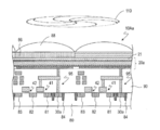
- FIG. 1 schematically illustrates the configuration of an imaging device according to a first embodiment of the present disclosure.
- the imaging device 100A illustrated in FIG. 1 includes a plurality of pixels 10A, a voltage supply circuit 50 electrically connected to the pixels 10A, and a signal processing circuit 60 that receives an output from the pixels 10A.
- the pixels 10A are, for example, two-dimensionally arranged to form an imaging region.
- four of the plurality of pixels 10A included in the imaging device 100A are extracted and shown. In the example shown in FIG. 1, these four pixels 10A have a 2 ⁇ 2 matrix arrangement.
- the number and arrangement of the pixels 10A in the imaging device 100A are arbitrary, and the number of the pixels 10A may be one.
- the imaging device 100A can function as a line sensor.
- each pixel 10A roughly includes a dielectric constant modulation element 20, a capacitive element 30, and a detection circuit 40.
- the dielectric constant modulation element 20 is an element including, in part thereof, a dielectric constant modulation structure which exhibits a property that the dielectric constant changes due to irradiation of light, and has a first terminal 21 and a second terminal 22.
- the dielectric constant modulation element 20 is irradiated with light to change, for example, the capacitance value between the first terminal 21 and the second terminal 22.
- An example of the configuration of the dielectric constant modulation element 20 will be described later.
- one electrode of the capacitive element 30 is electrically connected to the second terminal 22.
- the potential of the other electrode of the capacitive element 30 is fixed to the ground.
- the specific configuration of the capacitive element 30 is not limited to a specific configuration.
- the capacitive element 30 may be configured as a combined capacitance of a plurality of capacitive elements, or may be a combined capacitance by parallel connection or series connection of parasitic capacitances such as one or more capacitive elements and wiring.
- the capacitive element 30 can be designed to have a capacitance value equal to or higher than that of the dielectric constant modulation element 20 when compared in a dark state where light is not incident on the pixel 10A.
- the detection circuit 40 is electrically connected to the second terminal 22 and outputs a signal according to the potential of the second terminal 22.
- the detection circuit 40 includes a signal detection transistor 41 and an address transistor 42.
- the signal detection transistor 41 and the address transistor 42 are typically field effect transistors (FETs).
- FETs field effect transistors
- an N-channel MOS is exemplified as the signal detection transistor 41 and the address transistor 42.
- the gate of the signal detection transistor 41 is connected to the second terminal 22.
- the signal detection transistor 41 operates as a source follower by supplying a power supply voltage to its drain, for example. According to such a configuration, the potential of the second terminal 22 does not change even when the signal from the pixel 10A is read out. That is, the signal can be read out nondestructively.
- the source of the signal detection transistor 41 is connected to the output signal line 74 via the address transistor 42.
- the on and off of the address transistor 42 can be controlled, for example, by a row scanning circuit (not shown) via an address signal line provided for each row of the plurality of pixels 10A.
- the output signal line 74 is provided for each column of the plurality of pixels 10A and is connected to the signal processing circuit 60.
- the signal processing circuit 60 performs noise suppression signal processing represented by correlated double sampling, analog-digital conversion, and the like on the output signal read from the pixel 10A.
- the signal processing circuit 60 includes a plurality of analog-digital conversion circuits 62 (hereinafter simply referred to as "AD conversion circuits 62"). As illustrated, the AD conversion circuit 62 is provided for each output signal line 74. In other words, each AD conversion circuit 62 is connected to the corresponding output signal line 74.
- the output of the signal processing circuit 60 is read out of the imaging device 100A via, for example, an output circuit.
- the AD conversion circuit 62 may be disposed for each row or column of the plurality of pixels 10A, or may be disposed for each pixel 10A.
- the voltage supply circuit 50 is connected to the first terminal 21 of the dielectric constant modulation element 20 of each pixel 10A via the power supply line 70.
- the voltage supply circuit 50 supplies a predetermined voltage to each pixel 10A in operation.
- the voltage supply circuit 50 has a configuration capable of switching and supplying at least two different voltages to each pixel 10A. As will be described in detail later, the voltage supply circuit 50 applies a first voltage to the dielectric constant modulation element 20 in a first period, and generates a second voltage different from the first voltage in a second period different from the first period. The voltage is applied to the dielectric constant modulation element 20.
- the voltage supply circuit 50 is not limited to a specific power supply circuit, and may be a circuit that generates a predetermined voltage, or may be a circuit that converts a voltage supplied from another power supply into a predetermined voltage. .
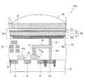
- FIG. 2 schematically illustrates an exemplary device structure of a pixel included in an imaging device of the present disclosure.
- the pixel 10Aa illustrated in FIG. 2 is an example of the above-described pixel 10A.
- FIG. 2 schematically shows the arrangement of the components constituting the pixel 10A, and the dimensions of the components shown in FIG. 2 do not necessarily reflect the dimensions of the actual device. The same applies to the other drawings of the present disclosure.
- the pixel 10Aa illustrated in FIG. 2 schematically includes a semiconductor substrate 80, an insulating layer 90 covering the semiconductor substrate 80, and a dielectric constant modulation element 20a supported by the insulating layer 90.
- Insulating layer 90 typically includes two or more insulating layers formed of silicon dioxide.
- the dielectric constant modulation element 20 a is an example of the above-described dielectric constant modulation element 20.
- an optical filter 86 such as a color filter, a microlens 88, and the like may be disposed above the dielectric constant modulation element 20a.
- the dielectric constant modulation element 20a faces the pixel electrode 22e supported by the insulating layer 90, the counter electrode 21e located farther from the semiconductor substrate 80 than the pixel electrode 22e, and the pixel electrode 22e. It includes a dielectric constant modulation structure 26a located between it and the electrode 21e.
- the counter electrode 21 e corresponds to the first terminal 21 of the dielectric constant modulation element 20 described above
- the pixel electrode 22 e corresponds to the second terminal 22.
- the pixel electrode 22e is electrically separated from the pixel electrode 22e of the adjacent other pixel 10Aa by being spatially separated from the adjacent other pixel 10Aa.
- a material of the pixel electrode 22e for example, a conductive material such as TiN or TaN which is stable and exhibits high light shielding property can be used.
- the counter electrode 21 e is formed of, for example, a translucent conductive material such as ITO.
- translucent in the present specification means that at least a part of the light in the wavelength range to be detected is transmitted, and it is essential to transmit the light over the entire wavelength range of visible light. Absent.
- the light detected by the imaging device of the present disclosure is not limited to light in the wavelength range of visible light, that is, light having a wavelength of 380 nm or more and 780 nm or less. In the present specification, all electromagnetic waves including infrared rays and ultraviolet rays are referred to as “light” for convenience.
- the counter electrode 21e is typically formed in the form of a single continuous electrode across the plurality of pixels 10Aa. Therefore, by connecting the power supply line 70 to the counter electrode 21 e, a desired voltage can be applied collectively to the counter electrodes 21 e of the plurality of pixels 10 Aa via the power supply line 70. Of course, it is not essential that the counter electrode 21e is continuous between all the pixels 10Aa. For example, the counter electrodes 21e may be separated for each row or column among the plurality of pixels 10Aa. .
- the light passing through the counter electrode 21e is incident on the dielectric constant modulation structure 26a.
- the dielectric constant modulation structure 26a is irradiated with light to change its dielectric constant. Detecting light through a change in dielectric constant in dielectric constant modulation structure 26 a by causing light to enter dielectric constant modulation structure 26 a in a state where a predetermined potential difference is given between pixel electrode 22 e and counter electrode 21 e Can. Details of the configuration of the dielectric constant modulation structure 26 a and details of the mechanism of light detection using the change of the dielectric constant in the dielectric constant modulation structure 26 a will be described later.
- the pixel electrode 22 e is electrically connected to the impurity region 30 a formed in the semiconductor substrate 80 through the connection portion 95 a disposed inside the insulating layer 90.
- a P-type silicon substrate is illustrated as the semiconductor substrate 80.
- the impurity region 30a is, for example, an N-type diffusion region.
- the junction capacitance formed by the pn junction including the impurity region 30 a can function as the above-described capacitance element 30.
- the semiconductor substrate 80 is not limited to a substrate that is entirely a semiconductor, and may be an insulating substrate or the like in which a semiconductor layer is provided on the surface on the side where the dielectric constant modulation element 20a is disposed.
- a signal detection transistor 41 and an address transistor 42 can be further formed.
- the plug 91 is connected to the gate electrode 41 g of the signal detection transistor 41.
- the plug 91 is connected to the plug 93 a connected to the above-described impurity region 30 a via the wiring 92. That is, the connection portion 95 a also has a connection with the gate electrode 41 g of the signal detection transistor 41.
- the plug 91 and the plug 93a are typically polysilicon plugs.
- the wire 92 is, for example, a polysilicon wire
- the plug 94 for connecting the wire 92 and the pixel electrode 22e to each other is, for example, a metal plug formed of copper or the like.
- Semiconductor substrate 80 further includes impurity regions 81, 82 and 83 and element isolation region 84.
- the impurity region 81 has a function as a drain region of the signal detection transistor 41
- the impurity region 82 has a function as a source region of the signal detection transistor 41.
- the address transistor 42 shares the impurity region 82 with the signal detection transistor 41, and the impurity region 82 also functions as a drain region of the address transistor 42.
- Impurity region 83 functions as a source region of address transistor 42.
- the above-mentioned output signal line 74 is connected to the impurity region 83.
- the output signal line 74 is not shown in FIG.
- An address signal line connected to the row scanning circuit is connected to the gate electrode 42 g of the address transistor 42.
- a wiring layer 96 is disposed in the insulating layer 90.
- the wiring layer 96 includes the output signal line 74 described above, an address signal line, and the like in part thereof.
- the dielectric constant modulation element 20a includes the dielectric constant modulation structure 26a sandwiched between the pixel electrode 22e and the counter electrode 21e.
- the dielectric constant modulation structure 26a has a laminated structure including the first charge blocking layer 23, the second charge blocking layer 24, and the photoelectric conversion layer 25 located between these blocking layers. .
- the photoelectric conversion layer 25 is irradiated with light to generate excitons inside.
- a typical example of the material of the photoelectric conversion layer 25 is a semiconductor material.
- an organic-semiconductor material is illustrated as a material which comprises the photoelectric converting layer 25.
- FIG. For example, a compound semiconductor material typified by hydrogenated amorphous silicon, CdSe or the like, or a metal oxide semiconductor material such as ZnO can be used as the material of the photoelectric conversion layer 25.
- the photoelectric conversion layer 25 may include a laminated structure of a donor organic compound and an acceptor organic compound, in other words, a heterojunction. Alternatively, a mixed layer having a bulk heterojunction structure may be included. The photoelectric conversion layer 25 may be a combination of these. The light incident on the photoelectric conversion layer 25 can be absorbed by either the donor organic compound or the acceptor organic compound or both of them.
- the first charge blocking layer 23 is located between the counter electrode 21 e and the photoelectric conversion layer 25, and suppresses exchange of charge between the counter electrode 21 e and the photoelectric conversion layer 25. That is, the first charge blocking layer 23 has a function of suppressing the movement of charges from the photoelectric conversion layer 25 to the counter electrode 21 e and the movement of charges from the counter electrode 21 e to the photoelectric conversion layer 25.
- the second charge blocking layer 24 is located between the pixel electrode 22e and the photoelectric conversion layer 25, and moves charge from the photoelectric conversion layer 25 to the pixel electrode 22e, and photoelectric conversion from the pixel electrode 22e. The transfer of charge to layer 25 is suppressed.
- the voltage supply circuit 50 applies a predetermined voltage to, for example, the counter electrode 21e, whereby a potential difference is given between the counter electrode 21e and the pixel electrode 22e. Therefore, the dielectric constant modulation structure 26a is in a state where an electric field is applied from the outside. Therefore, if, for example, the first charge blocking layer 23 is not provided in the dielectric constant modulation structure 26a, the counter electrode from the photoelectric conversion layer 25 when the counter electrode 21e has a high potential with respect to the pixel electrode 22e. The negative charge moves to 21 e, and the positive charge can move to the photoelectric conversion layer 25 from the counter electrode 21 e.
- the movement of charges between the photoelectric conversion layer 25 and the counter electrode 21 e is suppressed, and the photoelectric conversion layer is formed.
- the charge in 25 can be retained in the photoelectric conversion layer 25.
- the counter electrode 21e is set to a high potential with respect to the pixel electrode 22e
- by disposing the electron blocking layer as the first charge blocking layer 23 movement of electrons from the photoelectric conversion layer 25 to the counter electrode 21e can be performed. It can be restricted.
- a hole blocking layer as the second charge blocking layer 24 the movement of holes from the photoelectric conversion layer 25 to the pixel electrode 22e can be restricted.
- the photoelectric conversion layer 25 generates excitons in the photoelectric conversion layer 25 by the incidence of light through the counter electrode 21 e.
- excitons When excitons are generated in a state in which the movement of charge between the photoelectric conversion layer 25 and the electrode is suppressed, the charge density in the counter electrode 21 e and the pixel electrode 22 e is increased.
- the generation of excitons in a state where a potential difference is given between the counter electrode 21e and the pixel electrode 22e contributes to the change in polarization in the dielectric constant modulation structure 26a. Therefore, the increase in charge density at the electrodes results in an increase in the dielectric constant between the counter electrode 21e and the pixel electrode 22e, in other words, an increase in the dielectric constant of the dielectric constant modulation structure 26a.
- the capacitance value between the counter electrode 21 e and the pixel electrode 22 e is changed by the light irradiation.
- Light can be detected by detecting a change in the dielectric constant of the dielectric modulation structure 26a by means of the detection circuit 40, for example, in the form of a change in voltage.
- the photoelectric conversion layer 25 may be mainly made of an organic semiconductor material. That is, the dielectric constant modulation structure 26a may be a structure consisting essentially of an organic material.
- the materials of the first charge blocking layer 23 and the second charge blocking layer 24 are not limited to insulating materials. As described below, by appropriately selecting the material of the adjacent layer or electrode, the material which exhibits the property of transporting the charge of one polarity but not the charge of the opposite polarity by the application of voltage is selected as the first It can be used as a material of the charge blocking layer 23 and the second charge blocking layer 24.
- a hole transportable organic compound can be used as a material of the first charge blocking layer 23.
- a conductive material having a Fermi level shallower than the energy level of the highest occupied molecular orbital of the first charge blocking layer 23 as a material of the counter electrode 21 e
- a Schottky barrier between the electrode and the electrode It is possible to suppress both the movement of holes from the counter electrode 21 e to the first charge blocking layer 23 and the movement of electrons from the first charge blocking layer 23 to the counter electrode 21 e by using Similarly, when the counter electrode 21e is set to a high potential with respect to the pixel electrode 22e, an electron transporting organic compound can be used as a material of the second charge blocking layer 24.
- the second charge blocking layer from the pixel electrode 22 e Both the movement of electrons to 24 and the movement of holes from the second charge blocking layer 24 to the pixel electrode 22e can be suppressed.
- the energy level of the highest occupied molecular orbital may be simply referred to as the “HOMO level”
- the energy level of the lowest unoccupied molecular orbital may be simply referred to as the “LUMO level”.
- the photoelectric conversion layer 25 has a LUMO level of 4.0 eV and the pixel electrode 22 e is formed of an electrode material having a Fermi level of 5.1 eV.
- the above-described TiN is an electrode material having a Fermi level of about 5.1 to 5.2 eV, and can be applied to the material of the pixel electrode 22e.
- a hole blocking layer formed of an electron transporting organic compound can be used for the second charge blocking layer 24.
- the energy in the hole transport process between the photoelectric conversion layer 25 and the second charge blocking layer 24 As the barrier becomes larger, the ability to inhibit the movement of holes is improved.
- the fullerene has a LUMO level of 4.0 eV and a HOMO level of 6.4 eV. Therefore, it can be applied to the material of the second charge blocking layer 24 in this case.
- the energy barrier in the electron transport process is lowered as the LUMO level of the second charge blocking layer 24 is equal to or deeper than 4.0 eV, and the electron transport efficiency from the photoelectric conversion layer 25 toward the pixel electrode 22 e Improve.
- the counter electrode 21e has a high potential with respect to the pixel electrode 22e, and such movement of electrons may not be considered.
- the materials constituting the first charge blocking layer 23 and the second charge blocking layer 24 may be made of known materials in consideration of bond strength, stability, difference in ionization potential, difference in electron affinity, etc. between adjacent layers. It can be selected.
- the effect of retaining charges in the photoelectric conversion layer 25 can be obtained by providing the dielectric constant modulation structure 26 a with at least one of the first charge blocking layer 23 and the second charge blocking layer 24.
- the 1st charge blocking layer 23, the 2nd charge blocking layer 24, and the photoelectric converting layer 25 were organic materials was described, when these layers are inorganic compounds, it is HOMO. Is the valence band, and LUMO may be replaced with the conduction band.
- the HOMO level of the organic material can be determined, for example, by photoelectron spectroscopy, photoelectron yield spectroscopy, or the like.
- the LUMO level can be determined by inverse photoelectron spectroscopy or by subtracting the energy at the end of the absorption spectrum from the HOMO level.
- an insulating layer may be disposed instead of one or both of the first charge blocking layer 23 and the second charge blocking layer 24.
- the insulating layer may be disposed anywhere between the counter electrode 21 e and the photoelectric conversion layer 25 and between the pixel electrode 22 e and the photoelectric conversion layer 25.
- the insulating layer may be disposed both between the counter electrode 21 e and the photoelectric conversion layer 25 and between the pixel electrode 22 e and the photoelectric conversion layer 25.
- oxides such as SiO 2 , Al 2 O 3 , HfO 2 , and ZrO 2 , nitrides such as SiN, or compounds obtained by combination thereof, or polymethyl methacrylate resin (PMMA)
- PMMA polymethyl methacrylate resin
- FIG. 3 is an equivalent circuit diagram of the dielectric constant modulation element 20 a in the pixel 10 Aa and the impurity region 30 a as the capacitive element 30.
- the dielectric constant modulation structure 26a in the dielectric constant modulation element 20a changes its dielectric constant according to the amount of incident light. Further, since the dielectric constant modulation structure 26a includes the charge blocking layer or the insulating layer, basically no direct current flows between the dielectric constant modulation structure 26a and the pixel electrode 22e. From these things, in FIG. 3, the dielectric constant modulation element 20a is conveniently expressed using the circuit symbol similar to a variable capacitance.
- the voltage applied from the voltage supply circuit 50 to the first terminal 21 side of the dielectric constant modulation element 20a, that is, the counter electrode 21e is denoted as V IN .
- the voltage of the node M between the second terminal 22 side of the dielectric constant modulation element 20a, in other words, between the dielectric constant modulation element 20a and the capacitive element 30 (for example, the impurity region 30a) is denoted as V OUT .
- the detection circuit 40 described above is connected to the node M. Therefore, the above-described detection circuit 40 outputs a signal corresponding to the voltage V OUT .
- the set of the signal detection transistor 41 and the address transistor 42 shown in FIG. 1 is only an example of the detection circuit 40, and the configuration of the detection circuit 40 is as shown in FIG. 1 if it has the same function. It is not limited to.
- the charge density in the counter electrode 21e and the pixel electrode 22e increases due to the generation of excitons, and the capacitance value between the counter electrode 21e and the pixel electrode 22e changes. That is, the capacitance value C PC changes due to the light irradiation.
- the capacitance value C ref of the capacitance element 30 hardly changes due to the light irradiation to the pixel 10Aa, and the change of the capacitance value C ref due to the light irradiation is sufficiently compared with the change of the capacitance value C PC It is assumed that it is small. In this case, the voltage V OUT of the node M changes in accordance with the change of the capacitance value C PC of the dielectric constant modulation structure 26 a.
- FIG. 4 shows a change in V OUT with respect to a change in capacitance value C PC when a voltage of 5 V is applied as V IN and C ref is 1.2 fF.
- C PC capacitance value
- V OUT which is the potential of the second terminal 22 is also increased. Therefore, by connecting the detection circuit 40 to the node M, it is possible to detect a change in illuminance for the pixel 10Aa in the form of a change in input voltage to the signal detection transistor 41 as a source follower.
- the initial value of the capacitance value C PC for example, the capacitance value C PC of the dielectric constant modulation structure 26 a in a state where light is not irradiated is larger than the capacitance value C ref . If so, the change in the voltage V OUT with respect to the increase of the capacitance value C PC due to the light irradiation becomes small. Therefore, it is beneficial to have a relatively large capacitance value to the capacitive element 30 is capacitance C PC initial value.
- light can be detected through the change of the dielectric constant of the dielectric constant modulation element 20 due to the irradiation of light. Furthermore, in the embodiment of the present disclosure, unlike the configuration in which holes or electrons generated by photoelectric conversion are taken out as signal charges and the charge amount is read out, charges are not taken out from the dielectric constant modulation element 20. Therefore, by controlling the voltage applied from the voltage supply circuit 50 to the dielectric constant modulation element 20, for example, the potential difference between the counter electrode 21e and the pixel electrode 22e approaches 0V.
- the reset operation by the supply of the reset voltage can be basically eliminated.
- FIG. 5 is a timing chart to explain an exemplary operation of an imaging device according to an embodiment of the present disclosure.
- the uppermost graph shows the change of the voltage V IN supplied from the voltage supply circuit 50 to the power supply line 70
- the middle graph shows the potential V of the address signal line connected to the gate of the address transistor 42. Indicates a change in SEL .
- the lowermost graph shows changes in the voltage VAD for controlling the drive of the AD conversion circuit 62.
- the voltage supply circuit 50 has a configuration capable of switching at least two different voltages.
- the voltage supply circuit 50 can selectively supply either the high level first voltage or the low level second voltage lower than the first voltage to the power supply line 70.
- the voltage V OUT applied to the gate of the signal detection transistor 41 of the detection circuit 40 is the voltage V IN applied to the first terminal 21 of the permittivity modulation element 20, in other words
- the voltage supply circuit 50 is proportional to the voltage applied to the power supply line 70.
- the capacitance value C PC of the dielectric constant modulation structure 26a changes according to the illuminance, and the voltage V OUT also changes accordingly, but if the voltage V IN is small, the voltage V OUT accompanying the change of the illuminance Change is also small.
- the potential of the electrode of the capacitive element 30 not connected to the node M is the ground. Therefore, assuming that the low level second voltage is, for example, ground, ie, 0 V, the voltage V OUT applied to the gate of the signal detection transistor 41 is basically 0 V regardless of the illuminance. Therefore, it can be said that the period in which the voltage supply circuit 50 applies the low level second voltage to the power supply line 70 corresponds to the non-exposure period.
- the second voltage is applied to the power supply line 70 in the initial state.
- the second voltage is 0V.
- the voltage supply circuit 50 sets the voltage applied to the power supply line 70 to the high level first voltage.
- the voltage V IN applied to the counter electrode 21 e of the dielectric constant modulation element 20 a is made the first voltage
- the voltage V OUT has a capacitance value C corresponding to the illuminance, as can be seen from the equation (1) and FIG. It changes with the change of PC . That is, the voltage V OUT corresponding to the illuminance is applied to the gate of the signal detection transistor 41.
- the potential V SEL of the address signal line is set to the high level, and the address transistor 42 is turned on.
- a signal corresponding to the illuminance is output from the detection circuit 40 of the selected pixel 10A to the output signal line 74.
- a voltage signal corresponding to the illuminance is output to the output signal line 74.
- the drive pulse of the AD conversion circuit 62 is raised at time t3. That is, the AD conversion circuit 62 is operated in a state where the voltage supply circuit 50 supplies the high-level first voltage to the power supply line 70 and the address transistor 42 is turned on.
- the digital value obtained at this time by the operation of the AD conversion circuit 62 is the pixel signal corresponding to the illuminance in this example.
- the voltage supply circuit 50 switches the voltage supplied to the power supply line 70 to the low level second voltage.
- the voltage supplied to the power supply line 70 By switching the voltage supplied to the power supply line 70 to the second voltage, the potential difference between the counter electrode 21 e and the pixel electrode 22 e is reduced, and positive and negative generated in the photoelectric conversion layer 25 by light irradiation.
- the pair of charges quickly recombine.
- the voltage V OUT since the second voltage is 0V, the voltage V OUT is 0V. That is, the voltage V OUT applied to the gate of the signal detection transistor 41 returns to the state before the high level first voltage is supplied to the power supply line 70. That is, in the embodiment of the present disclosure, a period in which the voltage supply circuit 50 supplies a relatively high voltage to each pixel 10A can be regarded as an exposure period.
- the double arrow EXP in FIG. 5 schematically represents this exposure period.
- the drive pulse of the AD conversion circuit 62 is raised again.
- a digital value corresponding to the signal of the reference level before the high level first voltage is supplied to the power supply line 70 is obtained.
- the signal processing circuit 60 generates and outputs the difference between the digital value obtained at time t3 and the digital value obtained at time t5. That is, the signal processing circuit 60 generates a pixel signal obtained during a period in which the first voltage of high level is supplied to the power supply line 70 as a signal indicating the illuminance of the object, and a second voltage of low level to the power supply line 70. Generates a difference with the signal of the reference level obtained during the period in which Thereafter, at time t6, the address transistor 42 is turned off.
- the signal component thus obtained is compared with the case where the signal component obtained when a high level voltage is applied to the first terminal 21 is directly output as a signal indicating the illuminance of the object, The noise component is suppressed.
- the order of the detection of the pixel signal and the detection of the signal of the reference level is not limited to the example shown in FIG. 5, and the detection of the signal of the reference level may be performed first.
- the difference between the outputs of the detection circuit 40 is not limited to the form of the difference between the digital values, and may be, for example, the form of the difference between the amplitudes of the analog waveforms.
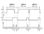
- FIG. 6 shows an example of an imaging operation over a plurality of frames.
- the voltage applied from the voltage supply circuit 50 to the power supply line 70 is set to the high level first voltage at time t11.
- the start of the application of the first voltage by the voltage supply circuit 50 corresponds to the start of the exposure period of the 0th frame period.
- the address transistor 42 is turned on at time t12. Further, by operating the AD conversion circuit 62 at time t13, a pixel signal according to the illuminance can be obtained.
- the voltage applied from the voltage supply circuit 50 to the power supply line 70 is switched to the low level second voltage.
- the timing of switching to the second voltage corresponds to the end of the exposure period in the zeroth frame period.
- the AD conversion circuit 62 is operated again at time t15, and a signal of the reference level is acquired. Thereafter, at time t16, the address transistor 42 is turned off, and the 0th frame period ends.
- the signal processing circuit 60 generates a difference between the pixel signal and the signal of the reference level obtained at time t15 as a signal indicating the illuminance of the subject.
- the voltage applied by the voltage supply circuit 50 to the power supply line 70 is again switched to the high level first voltage, whereby the next frame period, that is, the first frame period is started.
- the address transistor 42 is turned on at time t22, and the AD conversion circuit 62 is operated at time t23 to acquire a pixel signal corresponding to the illuminance for the first frame. .
- the voltage applied to the power supply line 70 is switched to the low level second voltage, and the address transistor 42 is turned off. Furthermore, the voltage applied to the power supply line 70 is switched to the first voltage again at time t31 without acquiring the signal of the reference level. In other words, the second frame period has begun.
- the signal processing circuit 60 generates a difference between the pixel signal obtained at time t23 and the signal of the reference level obtained at time t15 in the 0th frame period as a signal indicating the illuminance of the subject.
- the voltage V IN applied to the first terminal 21 is returned to the initial state, in other words, the voltage applied by the voltage supply circuit 50 to the power supply line 70 is low.
- the state of the dielectric constant modulation element 20 can be returned to the state before the light irradiation. That is, the potential of the node M can be substantially reset without executing the reset operation by supplying the reset voltage to the pixel.
- the operation in the subsequent second frame period may be similar to the operation in the first frame period.
- the address transistor 42 is turned on at time t32, and the AD conversion circuit 62 is operated at time t33 to obtain a pixel signal corresponding to the illuminance for the second frame.
- the voltage V IN is switched to the second voltage at time t34 and the address transistor 42 is turned off, whereby the second frame period ends.
- the point that the signal processing circuit 60 generates a difference between the pixel signal obtained at time t33 and the signal of the reference level obtained in the 0th frame period as a signal indicating the illuminance of the object is the first point. It is similar to the frame.
- the number of times the voltage supply circuit 50 reads the signal through the detection circuit 40 during the period in which the voltage supply circuit 50 supplies the second voltage to each pixel 10A. It may be less than the number of times the signal is read out through the detection circuit 40 during the period of supplying the first voltage. That is, the number of times of reading of the signal of the reference level may be smaller than the number of times of reading of the pixel signal according to the illuminance. According to such an operation, since acquisition of the signal of the reference level for each frame period is omitted, the period required for signal readout can be shortened and imaging can be performed at high speed. Alternatively, the exposure time can be lengthened by omitting the acquisition of the signal of the reference level for each frame period, and a higher SN ratio can be realized.
- FIG. 7 schematically illustrates an example of the read operation of the imaging device including a plurality of pixels arranged in two dimensions.
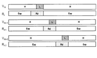
- the white rectangle H in the top row represents the first period during which the voltage supply circuit 50 applies the first voltage of high level to the first terminal 21, and the hatched rectangle L represents the voltage supply circuit. 50 represents a second period in which a low level second voltage is applied to the first terminal 21.
- a common voltage is applied to the counter electrode 21e of each pixel 10Aa.
- FIG. 7 representatively shows operations of a pixel belonging to the i-th row, a pixel belonging to the (i + 1) -th row, and a pixel belonging to the (i + 2) -th row among a plurality of rows.
- white rectangles Exp represent exposure periods in each row
- shaded rectangles Rd represent signal readout periods.
- the readout of the pixel signal and the readout of the signal of the reference level are executed at the timing represented by the rectangle Rd.
- the readout of the pixel signal is performed in the first period, and the readout of the signal of the reference level is performed in the second period.
- acquisition of a signal of a reference level for each frame period may be omitted.
- readout of the pixel signal and the signal of the reference level is sequentially performed while shifting the timing on a row basis.
- FIG. 8 schematically shows another example of the readout operation of the imaging device including a plurality of pixels arranged in a two-dimensional manner.
- the shaded rectangle Rd1 represents the readout period of the pixel signal
- the shaded rectangle Rd2 represents the readout period of the signal of the reference level.
- readout of pixel signals is sequentially performed in row units in a first period
- readout of signals of a reference level is sequentially performed in row units in a second period.
- voltage switching from the first voltage to the second voltage and switching from the second voltage to the first voltage may be performed once in one frame period.
- FIG. 9 and FIG. 10 schematically show still another example of the readout operation of the imaging device including a plurality of pixels arranged in two dimensions.
- signal readout is performed at common timing for all the rows, and the start and end of the exposure period are common to all the pixels. That is, a so-called global shutter is realized.
- the signal processing circuit 60 and an XY decoder for designating a specific pixel in the imaging area are arranged on a chip different from the chip in which the imaging area is formed. For example, these chips are stacked. This can be realized by electrically connecting each row of a plurality of pixels to the signal processing circuit 60. An analog-digital conversion circuit may be arranged in each pixel. According to the chip stacking technology, it is possible to realize an imaging device adapted to such a reading method while avoiding an increase in size of a pixel.
- FIG. 10 shows an operation example applicable to a pixel having a frame memory.
- a shaded rectangle Trs represents a period for transferring information on the signal level to the frame memory.
- FIG. 10 shows an example in which the voltage level of the pixel signal obtained in the exposure period is transferred to the frame memory, and the voltage level of the pixel signal is read out from the frame memory during the exposure period of the next frame period. Note that the reading of the signal of the reference level may be performed in the second period in any frame period.
- FIG. 11 shows an example of a pixel having a frame memory.
- the pixel 10B shown in FIG. 11 includes a set of a transfer transistor 45 connected between the node M and the gate of the signal detection transistor 41, and a capacitive element 44 having one electrode connected to the gate of the signal detection transistor 41. .
- the other electrode of the capacitor 44 for example by being connected to a power supply (not shown), capable of applying configured the predetermined voltage V G during operation of the imaging apparatus 100A.
- the voltage level of the node M after exposure can be temporarily held by the capacitive element 44 by turning on the transfer transistor 45 after the lapse of a predetermined period from the start of the first period and turning it off again. After the voltage level is held in the capacitive element 44, a signal corresponding to the voltage level held in the capacitive element 44 can be read out to the output signal line 74 at a desired timing by turning on the address transistor 42. .
- the transfer transistor 45 and off can be controlled, for example, by a row scanning circuit (not shown). From the viewpoint of increasing sensitivity, it is useful that the capacitive element 44 have a capacitance value smaller than that of the capacitive element 30 (for example, the impurity region 30a).
- the potential of the node M is substantially 0 V regardless of light irradiation. Therefore, the reset operation required for a general imaging device is basically unnecessary.
- the voltage applied to the electrode on the side not connected to the node M among the electrodes of the capacitive element 30 and the second voltage applied to the dielectric constant modulation element 20 by the voltage supply circuit 50 do not match. I assume. In such a case, when the voltage applied to the dielectric constant modulation element 20 is switched to the first voltage, the potential of the node M can rise from 0 V even without light irradiation.
- the signal processing circuit 60 may obtain the pixel signal obtained during the period in which the first voltage of high level is supplied to the power supply line 70 and the period during which the second voltage of low level is supplied to the power supply line 70.
- a signal obtained by further subtracting the signal corresponding to the offset level from the difference from the signal of the reference level may be output as a signal indicating the illuminance of the subject.
- the subtraction of the signal corresponding to the offset level may be performed in the form of subtraction of digital signals or may be performed in the form of subtraction of analog signals. By subtracting the signal corresponding to the offset level, it is possible to reduce fixed pattern noise due to the variation of the offset level for each pixel.
- the signal corresponding to the offset level is not irradiated with light to the dielectric constant modulation element 20, and the detection circuit 40 is in a state in which the high-level first voltage is supplied from the voltage supply circuit 50 to the power supply line 70. It is a signal to be output. As described below, the signal corresponding to the offset level can be obtained by various methods.
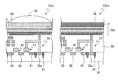
- FIG. 12 shows a first example of a configuration capable of acquiring a signal corresponding to the offset level.
- the imaging device has an array of a plurality of pixels including a dummy pixel 10Dm in addition to the above-described pixel 10Aa.
- the light shielding layer 28 covers the dielectric constant modulation element 20a and blocks the incidence of light on the dielectric constant modulation element 20a.
- the basic device structure of the dummy pixel 10Dm is similar to that of the pixel 10Aa except that it has the light shielding layer 28.
- the optical filter 86 and the micro lens 88 can be abbreviate
- Incident of light to the dielectric constant modulation element 20 a of the dummy pixel 10 Dm is prevented by the light shielding layer 28. Therefore, by reading out the output of the detection circuit 40 of the dummy pixel 10Dm in the state where the first voltage is applied to the counter electrode 21e, a signal corresponding to the offset level can be obtained with a relatively simple configuration.
- Such dummy pixels 10Dm may be arranged in the peripheral area outside the imaging area formed from the array of the pixels 10Aa. Such a configuration is effective particularly when the influence of the variation in the offset level for each pixel is small.
- FIG. 13 shows a second example of a configuration capable of acquiring a signal corresponding to the offset level.
- the imaging device has a mechanical shutter 110 that switches the incidence and blocking of light to each pixel 10Aa.
- a pixel signal can be obtained through the detection circuit 40.
- a signal corresponding to the offset level can be obtained by acquiring the output from the detection circuit 40 in a state in which the first voltage is applied to the counter electrode 21e and in a state in which the mechanical shutter 110 is closed.
- the mechanical shutter 110 that operates in synchronization with the signal processing circuit 60 may be used to obtain a signal corresponding to the offset level. According to the second example described here, even if the offset level is different for each pixel, it is possible to accurately obtain the offset.
- FIG. 14 shows a third example of the configuration capable of acquiring a signal corresponding to the offset level.
- An imaging device 100B illustrated in FIG. 14 includes a light source 120 and a control circuit 130 that synchronously drives the light source 120 and the plurality of pixels 10Aa.
- the light source 120 irradiates the object Ob with light of a predetermined wavelength range, for example, infrared light, in the first period in which the high level first voltage is applied to the counter electrode 21 e.
- the plurality of pixels 10Aa output a signal based on the reflected light of a predetermined wavelength range from the subject Ob.
- the signal detected by the detection circuit 40 of the pixel 10Aa in a state in which the light source 120 is turned off and the first voltage of high level is applied to the counter electrode 21e corresponds to the signal corresponding to the offset level.
- the configuration as illustrated in FIG. 14 is also useful.
- the configuration as illustrated in FIG. 14 is particularly useful when detecting light in a wavelength range in which the intensity included in ambient light is small.
- infrared light having a wavelength of about 900 nm or more for indoor photographing and about 1400 nm for outdoor photographing can be used as light emitted from the light source 120.
- the detection circuit of each pixel 10Aa in the state where the light source 120 is turned off and the first voltage of high level is applied to the counter electrode 21e.
- the signal detected by 40 gives the correct value of the signal corresponding to the offset level.
- All of the first to third examples are examples in which an output corresponding to the signal level in the dark is used as a signal corresponding to the offset level.
- the voltage supply circuit 50 switches the voltage applied to the power supply line 70 from the low level second voltage to the high level first voltage, in other words, detection is performed at the very beginning of the first period corresponding to the exposure period.
- the signal output from the circuit 40 may be acquired as a signal corresponding to the offset level.
- an offset level corresponding to each pixel can be obtained.
- the signal corresponding to the offset level for each pixel may be read once at a timing different from that for reading the pixel signal.
- the potential of the node M may be obtained in advance for each pixel under dark conditions, and a signal corresponding to the potential obtained at this time may be used as a signal corresponding to the offset level.
- a memory may be provided in the signal processing circuit 60, and the value of the offset level may be held in advance in the memory.
- a configuration may be adopted in which the value of the offset level in the memory is updated by performing calibration at an arbitrary timing. If the variation in the offset level for each pixel is small, the common offset level may be uniformly applied to all the pixels.
- FIG. 15 shows a modification in which a reset transistor is provided in a pixel.
- the pixel 10C illustrated in FIG. 15 includes a reset transistor 46 connected to the node M.
- one of the source and the drain of the reset transistor 46 is electrically connected to a terminal (for example, the pixel electrode 22e) connected to the node M of the permittivity modulation element 20a.
- the other of the source and the drain of the reset transistor 46 is supplied with a predetermined reset voltage VRef .
- the reset transistor 46 is turned on, the potential of the pixel electrode 22e, in other words, the potential of the node M, is reset to V Ref .
- the on and off of the reset transistor 46 is controlled, for example, by applying a reset signal V RST to the gate of the reset transistor 46 from a row scanning circuit (not shown).
- the charge generated by photoelectric conversion is not extracted to the node M and stored in the node M.
- the voltage V IN applied to the terminal (for example, the counter electrode 21 e) opposite to the node M of the dielectric constant modulation element 20 a to, for example, 0 V
- the voltage V OUT of the node M in other words, If so, the input to the detection circuit 40 can be 0V. Therefore, if the voltage supply circuit 50 switches the voltage applied to the power supply line 70 from the high level first voltage to the low level second voltage, exposure of the next frame is performed without applying the reset voltage to the node M. Can be started.
- the voltage applied to the first terminal 21 by the voltage supply circuit 50 is switched between the first voltage and the second voltage, Light can be detected by the detection circuit 40 detecting the potential of the node M in each of a first period in which the first voltage is supplied to the pixel and a second period in which the second voltage is supplied.
- a circuit for resetting the node M is basically unnecessary.
- the charge amount in the node M can be made uniform among a plurality of pixels.
- the potential of the node M before exposure can be adjusted to an arbitrary value among a plurality of pixels, and the variation in reference level for each pixel can be eliminated. Therefore, the advantage is obtained that the voltage range can be used effectively.
- the potential of the pixel electrode 22e after reset can be made equal to the potential of the counter electrode 21e.
- the reset voltage V Ref may be the same voltage as the second voltage.
- the voltage supply circuit 50 applies the second voltage to the counter electrode 21e in the second period, and the reset voltage V Ref is equal to the second voltage, the potential difference applied to the permittivity modulation structure 26a after the reset operation is approximately 0 V It is possible. Therefore, it is also possible to make the sensitivity of a specific pixel zero at any time.
- the reset voltage V Ref is supplied to the pixel electrode 22e by turning on the reset transistor 46 in the second period in which the second voltage is supplied to the pixel 10C. Reset of the potential of the pixel electrode 22e is performed.
- the readout of the signal of the reference level via the detection circuit 40 is performed after the reset of the potential of the pixel electrode 22 e by the reset transistor 46. As described above, readout of the signal of the reference level is performed, for example, once in the second period before the first frame period starts or in the second period in the first frame period among a plurality of consecutive frames. do it.
- the exposure period of the first frame period starts.
- the potential of the node M returns to V Ref .
- FIG. 16 shows another example of the device structure of a pixel.
- the difference between the pixel 10Ab shown in FIG. 16 and the pixel 10Aa shown in FIG. 2 is that the pixel 10Ab is disposed in the insulating layer 90 instead of the impurity region 30a as the capacitive element 30, MIM (metal a point having the capacitive element 30b of the (insulator-metal) structure.
- MIM metal a point having the capacitive element 30b of the (insulator-metal) structure.
- capacitive element 30 b includes upper electrode 33, lower electrode 34 located between upper electrode 33 and semiconductor substrate 80, and dielectric sandwiched between upper electrode 33 and lower electrode 34. It has a layer 35.
- the connection portion 95b in the pixel 10Ab includes a plug 93b that electrically connects the upper electrode 33 and the wiring 92 to each other.
- the lower electrode 34 is connected to a wire (not shown), its potential is fixed, for example, to ground during operation.
- the capacitive element 30 connected to the node M is not limited to the form of the junction capacitance formed by the pn junction, and may be realized in the form of an MIM structure like the capacitive element 30b. It may be realized in the form of a MOS capacitor in which the electrode is a semiconductor layer. When the MIM structure is applied, a part of the wiring layer 96 may be used as one or both of the upper electrode 33 and the lower electrode 34.
- the material of the dielectric layer 35 is, for example, an oxide such as SiO 2 , Al 2 O 3 , HfO 2 , ZrO 2 or a nitride such as SiN, or a compound obtained by a combination thereof, PMMA, polyimide And organic materials such as polystyrene can be widely used.
- a combination of different materials may form substantially one capacitive element.
- part of the insulating layer 90 may be used as the dielectric layer 35.
- the MIM structure of the capacitive element 30b is also referred to as a MOM structure.
- the capacitance element 30b has a structure in which the capacitance value hardly changes even when light is incident, or the change in capacitance value due to the light incidence is sufficiently smaller than the change in capacitance value in the dielectric constant modulation element 20a. It is formed as For example, as a material of the dielectric layer 35, a material such as SiO 2 whose dielectric constant hardly changes upon light incidence may be selected. Alternatively, TiN having high light shielding properties can be applied as a material of the upper electrode 33 and / or the lower electrode 34.
- the capacitive element 30 b may be disposed in the insulating layer 90 so that the periphery is covered with a light shielding material, and the incidence of light to the capacitive element 30 b may be suppressed.
- node M includes the interface between the silicon substrate and the contact plug. Absent. Therefore, it is possible to avoid the influence of dark current caused by interface states. If the reset transistor 46 is formed as a thin film transistor, generation of dark current due to the interface state can be avoided even in combination with the reset circuit including the reset transistor 46.
- the configuration of the dielectric constant modulation element 20 is also not limited to the configuration described with reference to FIG.
- a layer including quantum dots may be applied instead of the photoelectric conversion layer 25 in the dielectric constant modulation structure 26 a shown in FIG. 2. Quantum dots receive light incident to generate charge pairs. Also in this case, as in the example shown in FIG. 2, transfer of the insulating layer or charge to at least one of the layer including the quantum dot and the counter electrode 21 e and between the layer including the quantum dot and the pixel electrode 22 e A charge blocking layer is provided to suppress
- FIG. 17 shows another example of the dielectric constant modulation element 20.
- the pixel 10D shown in FIG. 17 includes a counter electrode 21e, a pixel electrode 22e, and a dielectric constant modulation element 20d including a dielectric constant modulation structure 26d located between the counter electrode 21e and the pixel electrode 22e.
- the dielectric constant modulation structure 26d is a layer including a material whose dielectric constant changes by light irradiation, such as hafnium oxide. With such a configuration as well, it is possible to detect light through the change of the dielectric constant of the dielectric constant modulation element 20d due to the light irradiation.
- the response of the dielectric constant in the dielectric constant modulation element 20 to the incidence of light may be nonlinear or linear with respect to the intensity or time of the incident light. In any case, light detection is possible.
- a dielectric constant modulation structure that exhibits a larger change in dielectric constant with respect to light irradiation as the potential difference between the counter electrode 21 e and the pixel electrode 22 e becomes larger. Since the amount of change of the dielectric constant between the time of detection of the signal is expanded, more sensitive detection can be performed.
- FIG. 18 schematically illustrates the configuration of an imaging device according to the second embodiment of the present disclosure.
- the imaging device 100E shown in FIG. 18 has a plurality of pixels 10E instead of the plurality of pixels 10A.
- the electrode not connected to the second terminal 22 of the dielectric constant modulation element 20 is a voltage supply circuit through the power supply lines 71 and 72. It is electrically connected to 50. That is, in this example, the voltage supply circuit 50 is configured to be capable of switching and supplying the first voltage and the second voltage to the second terminal 22 of the dielectric constant modulation element 20 via the capacitive element 30.
- the potential of the first terminal 21 is commonly fixed to, for example, the ground during operation.
- the voltage V OUT exhibits a decreasing change.
- the signal detection transistor 41 as a source follower is irradiated with light.
- the detection circuit 40 can detect the change in the dielectric constant of the dielectric constant modulation element 20 in the form of a voltage change.
- the voltage supply circuit 50 is configured to change the potential on the first terminal 21 side with reference to the potential on the second terminal 22 side of the dielectric constant modulation element 20 as in this example. It is also possible to change the potential of the electrode of the capacitive element 30 on the side not connected to the second terminal 22 based on the potential on the first terminal 21 side of the dielectric constant modulation element 20 as a reference. .
- the voltage supply circuit 50 may be configured such that a predetermined voltage can be applied to the other terminal with reference to either the first terminal 21 or the second terminal 22 of the dielectric constant modulation element 20.
- the voltage supply circuit 50 supplies a voltage to either the first terminal 21 side or the electrode on the side not connected to the second terminal 22 of the electrodes of the capacitive element 30, thereby the first terminal 21 and the second terminal 22.
- the potential difference between and can be uniquely determined.
- the potential difference applied to dielectric constant modulation structure 26a or 26d is also uniquely determined.
- the capacitive element 30 is interposed between the second terminal 22 of each pixel 10E and the voltage supply circuit 50, but the voltage supplied by the voltage supply circuit 50 causes the first terminal 21 and It can be said that the potential difference with the second terminal 22 is substantially controlled.
- the power supply line 71 is connected to the capacitive elements 30 of the two pixels 10E belonging to the first row, and the capacitive elements 30 of the two pixels 10E belonging to the second row are electrically Line 72 is connected. Therefore, according to such a form of connection, the potential of node M can be individually controlled on a row basis.
- FIG. 19 schematically shows an example of the read operation in the imaging device 100E shown in FIG.
- the relationship between the change in V IN and the exposure period and the readout period is also shown.
- a shaded rectangle Rd represents a period during which the readout of the pixel signal and the readout of the signal of the reference level are performed.
- the readout of the pixel signal is performed in the first period, and the readout of the signal of the reference level is performed in the second period, as in the example described with reference to FIG.
- switching between the first voltage and the second voltage can be performed at any timing, for example, for each row. It is possible to carry out. Therefore, as shown in FIG. 19, it is possible to apply the readout operation similar to a so-called rolling shutter by shifting the period of switching between the first voltage and the second voltage and readout of the signal for each row.
- the readout operation similar to a so-called rolling shutter by shifting the period of switching between the first voltage and the second voltage and readout of the signal for each row.
- the exposure period can be expanded to enable imaging with an improved SN ratio.
- Such switching of voltages in units of rows can also be realized by patterning the counter electrode 21 e so as to be separated by each row of a plurality of pixels in a configuration in which the power supply line 70 is connected to the counter electrode 21 e.
- the power supply lines 71 and 72 are provided independently for each row of the plurality of pixels 10E, and switching between the first voltage and the second voltage is performed independently for each row.
- the invention is not limited to the example, and power supply lines connected to the voltage supply circuit 50 may be connected to each column of the plurality of pixels 10E or to each of the pixels 10E independently. That is, the voltage supply circuit 50 may be configured to be able to independently supply different voltages in units of columns or in units of pixels, and the potential of the node M may be individually controlled in units of columns or in units of pixels.
- FIG. 20 schematically illustrates an exemplary configuration of an imaging device according to a third embodiment of the present disclosure.
- An imaging device 100F illustrated in FIG. 20 includes an imaging element 200 and a signal processing circuit 60F that performs signal processing on an electrical signal from the imaging element 200.
- the image pickup device 200 includes, for example, a plurality of pixels 10A as in the above-described image pickup apparatus 100A, converts incident light into an electric signal, and outputs the electric signal to the signal processing circuit 60F.
- the imaging device 200 further includes a voltage supply circuit 50 that supplies a predetermined voltage to each of the pixels 10A.
- the point that the second voltage is supplied in different second periods is the same as each of the above-described examples.
- the signal processing circuit 60F is a pixel signal obtained during a period in which the high-level first voltage is supplied to the power supply line connected to the voltage supply circuit 50; A difference from the signal of the reference level obtained during the period in which the low level second voltage is supplied to the power supply line is generated and output.
- the signal processing circuit 60F is typically provided with AD conversion circuits 62 in the same number as the number of columns of the plurality of pixels 10A. In FIG. 20, two of these AD conversion circuits 62 are representatively shown for simplicity.
- the signal processing circuit 60F is a circuit substrate different from the semiconductor substrate 80. It is provided at 89.
- some circuits including the AD conversion circuit 62 may be formed on a substrate different from the substrate on which the pixels are arranged. For example, one camera system can be constructed by stacking these two substrates and electrically connecting them.
- the voltage supply circuit 50 sets the first voltage and the second voltage at one of the first terminal 21 and the second terminal 22 of the dielectric constant modulation element 20 as a reference.
- the voltage supply circuit 50 supplies the first voltage of high level to each pixel in the exposure period, and supplies the second voltage of low level to each pixel in the period of readout of the reference level.
- the detection circuit 40 reads the pixel signal at the level corresponding to the illuminance during the first period in which the voltage supply circuit 50 supplies the first voltage, and the voltage supply circuit 50 supplies the second voltage. During a period, readout of the signal of the reference level is performed.
- the first voltage and / or the second voltage may be applied as a pulse, or the application may be repeated periodically or quasi-periodically.
- Example 1 A sample imitating the above-described dielectric constant modulation element 20 was manufactured, the bias was changed, and the capacitance value was measured to evaluate the change in the dielectric constant with respect to the illuminance in the manufactured sample.
- FIG. 21 schematically shows the structure of a sample produced as Example 1. The samples were prepared as follows.
- a glass substrate 90S was prepared.
- the lower electrode 22S and the insulating layer 24S were formed on the glass substrate by sequentially depositing ITO and Al 2 O 3 on the glass substrate by sputtering and atomic layer deposition (ALD), respectively.
- ALD atomic layer deposition
- a tin naphthalocyanine (SnNc) and a fullerene (C 60 ) were sequentially deposited by vapor deposition to form a photoelectric conversion layer 25S.
- the thickness of each of the tin naphthalocyanine layer and the fullerene layer was approximately 75 nm.
- Example 1 After formation of the photoelectric conversion layer 25S, Al 2 O 3 and ITO were further deposited successively on the photoelectric conversion layer 25S by ALD and sputtering to form a laminated structure of the insulating layer 23S and the top electrode 21S.
- the sample of Example 1 was obtained by the above procedure.
- the thickness of the insulating layers 24S and 23S was about 20 nm
- the thickness of the photoelectric conversion layer 25S was about 150 nm
- the thickness of the top electrode 21S was about 50 nm.
- the bias V bias applied between the lower surface electrode 22S and the upper surface electrode 21S is changed to measure the current response to the AC voltage.
- the capacitance value between the and the top electrode 21S was measured.
- a capacitance value was measured in the sequential mode using an AC voltage amplitude of 100 mV and a measurement frequency of 100 Hz using a precision LCR meter 4284A manufactured by HEWLETT PACKARD.
- FIG. 22 shows, for each bias, the measurement results of the change in capacitance value when the illuminance is changed, with respect to the sample of Example 1.
- the horizontal axis of the graph shown in FIG. 22 indicates the intensity of light irradiated to the sample, and the vertical axis indicates the capacitance value between the lower surface electrode 22S and the upper surface electrode 21S.
- the unit of light intensity shown in FIG. 22 is an arbitrary unit.
- the imaging device of the present disclosure is applicable to an image sensor and the like. In particular, it is useful for an image sensor for detecting light in the infrared region susceptible to dark current.
- the imaging device of the present disclosure can be used for digital cameras, medical cameras, camera for machine vision (for example, cameras for robots), and the like.
- the machine vision camera can be used, for example, as an input for performing image recognition to determine the state of a product at a production plant, classification, or detection of a defect.
- Embodiments of the present disclosure are also useful for security cameras, cameras mounted on vehicles and the like.
- the on-vehicle camera may be used, for example, as an input to a control device for the vehicle to travel safely. Alternatively, it can be used to assist the operator for the vehicle to travel safely.
- An infrared image can be used, for example, for sensing such as distance detection and object recognition.
Landscapes
- Engineering & Computer Science (AREA)
- Physics & Mathematics (AREA)
- Power Engineering (AREA)
- General Physics & Mathematics (AREA)
- Electromagnetism (AREA)
- Condensed Matter Physics & Semiconductors (AREA)
- Computer Hardware Design (AREA)
- Microelectronics & Electronic Packaging (AREA)
- Signal Processing (AREA)
- Multimedia (AREA)
- Solid State Image Pick-Up Elements (AREA)
- Transforming Light Signals Into Electric Signals (AREA)
- Light Receiving Elements (AREA)
Abstract
L'invention concerne un dispositif d'imagerie qui est pourvu de pixels comprenant chacun : un élément de modulation de permittivité comprenant une première borne, une seconde borne, et une structure de modulation de permittivité située entre la première borne et la seconde borne et présentant une permittivité qui change par irradiation de lumière; un élément capacitif comprenant une première électrode et une seconde électrode, la seconde électrode étant électriquement connectée à la seconde borne de l'élément de modulation de permittivité; et un circuit de détection qui délivre en sortie un signal correspondant au potentiel de la seconde borne. Le dispositif d'imagerie est en outre pourvu d'un circuit d'alimentation en tension qui applique une première tension à l'une de la première borne de l'élément de modulation de permittivité et de la première électrode de l'élément capacitif pendant une première période, et lui applique une seconde tension pendant une seconde période différente de la première période, et un circuit de traitement de signal qui génère un troisième signal qui est une différence entre un premier signal délivré en sortie par le circuit de détection pendant la première période et un second signal délivré en sortie par le circuit de détection pendant la seconde période, et une différence de potentiel entre la première borne et la première électrode lorsque la seconde tension est appliquée à celle-ci est inférieure à une différence de potentiel entre la première borne et la première électrode lorsque la première tension est appliquée à celle-ci.
Priority Applications (4)
| Application Number | Priority Date | Filing Date | Title |
|---|---|---|---|
| JP2019562914A JP7145438B2 (ja) | 2017-12-28 | 2018-12-06 | 撮像装置 |
| EP18895292.3A EP3734965B1 (fr) | 2017-12-28 | 2018-12-06 | Dispositif d'imagerie |
| CN201880048460.8A CN110945865B (zh) | 2017-12-28 | 2018-12-06 | 摄像装置 |
| US16/906,446 US11317043B2 (en) | 2017-12-28 | 2020-06-19 | Imaging device |
Applications Claiming Priority (2)
| Application Number | Priority Date | Filing Date | Title |
|---|---|---|---|
| JP2017253343 | 2017-12-28 | ||
| JP2017-253343 | 2017-12-28 |
Related Child Applications (1)
| Application Number | Title | Priority Date | Filing Date |
|---|---|---|---|
| US16/906,446 Continuation US11317043B2 (en) | 2017-12-28 | 2020-06-19 | Imaging device |
Publications (1)
| Publication Number | Publication Date |
|---|---|
| WO2019131028A1 true WO2019131028A1 (fr) | 2019-07-04 |
Family
ID=67066406
Family Applications (1)
| Application Number | Title | Priority Date | Filing Date |
|---|---|---|---|
| PCT/JP2018/044808 WO2019131028A1 (fr) | 2017-12-28 | 2018-12-06 | Dispositif d'imagerie |
Country Status (5)
| Country | Link |
|---|---|
| US (1) | US11317043B2 (fr) |
| EP (1) | EP3734965B1 (fr) |
| JP (1) | JP7145438B2 (fr) |
| CN (1) | CN110945865B (fr) |
| WO (1) | WO2019131028A1 (fr) |
Cited By (3)
| Publication number | Priority date | Publication date | Assignee | Title |
|---|---|---|---|---|
| WO2022102343A1 (fr) * | 2020-11-13 | 2022-05-19 | パナソニックIpマネジメント株式会社 | Dispositif d'imagerie |
| US11696051B2 (en) | 2019-08-01 | 2023-07-04 | Panasonic Intellectual Property Management Co., Ltd. | Imaging device |
| WO2024062746A1 (fr) * | 2022-09-22 | 2024-03-28 | パナソニックIpマネジメント株式会社 | Dispositif d'imagerie et circuit de traitement |
Families Citing this family (3)
| Publication number | Priority date | Publication date | Assignee | Title |
|---|---|---|---|---|
| WO2019155841A1 (fr) * | 2018-02-07 | 2019-08-15 | ソニーセミコンダクタソリューションズ株式会社 | Capteur d'image à semi-conducteurs, et dispositif d'imagerie |
| CN112420768B (zh) * | 2020-11-09 | 2022-11-08 | 电子科技大学 | 一种可切换红外光电记忆与探测功能的晶体管及制备方法 |
| CN112947787A (zh) * | 2021-02-23 | 2021-06-11 | 北京京东方显示技术有限公司 | 触控面板、显示装置、显示系统及触控方法 |
Citations (5)
| Publication number | Priority date | Publication date | Assignee | Title |
|---|---|---|---|---|
| JP2011060830A (ja) | 2009-09-07 | 2011-03-24 | Japan Advanced Institute Of Science & Technology Hokuriku | 光照射によって誘電率が変化する膜およびそれを用いた電子デバイス |
| JP2016086407A (ja) * | 2014-10-23 | 2016-05-19 | パナソニックIpマネジメント株式会社 | 撮像装置および画像取得装置 |
| WO2017081831A1 (fr) | 2015-11-12 | 2017-05-18 | パナソニックIpマネジメント株式会社 | Capteur optique |
| WO2017081847A1 (fr) | 2015-11-12 | 2017-05-18 | パナソニックIpマネジメント株式会社 | Dispositif de détection de lumière |
| JP2017175108A (ja) * | 2016-03-17 | 2017-09-28 | パナソニックIpマネジメント株式会社 | 光センサおよび撮像装置 |
Family Cites Families (15)
| Publication number | Priority date | Publication date | Assignee | Title |
|---|---|---|---|---|
| JP2009212618A (ja) | 2008-02-29 | 2009-09-17 | Fujifilm Corp | 画像検出装置 |
| JP5129650B2 (ja) | 2008-05-23 | 2013-01-30 | キヤノン株式会社 | 撮像装置 |
| JP6065732B2 (ja) | 2013-04-24 | 2017-01-25 | 株式会社島津製作所 | 画像処理装置および撮影装置 |
| JP6425448B2 (ja) | 2014-07-31 | 2018-11-21 | キヤノン株式会社 | 光電変換装置、および、撮像システム |
| JP6213743B2 (ja) | 2014-10-08 | 2017-10-18 | パナソニックIpマネジメント株式会社 | 撮像装置およびその駆動方法 |
| US9967501B2 (en) * | 2014-10-08 | 2018-05-08 | Panasonic Intellectual Property Management Co., Ltd. | Imaging device |
| JP6777421B2 (ja) * | 2015-05-04 | 2020-10-28 | 株式会社半導体エネルギー研究所 | 半導体装置 |
| US9860465B2 (en) * | 2015-06-23 | 2018-01-02 | Semiconductor Energy Laboratory Co., Ltd. | Imaging device and electronic device |
| US10373991B2 (en) * | 2015-08-19 | 2019-08-06 | Semiconductor Energy Laboratory Co., Ltd. | Imaging device, operating method thereof, and electronic device |
| CN107004690B (zh) | 2015-11-12 | 2021-05-14 | 松下知识产权经营株式会社 | 光传感器 |
| JP2017168812A (ja) * | 2016-03-10 | 2017-09-21 | パナソニックIpマネジメント株式会社 | 撮像装置 |
| JP2017220577A (ja) * | 2016-06-08 | 2017-12-14 | パナソニックIpマネジメント株式会社 | 光検出装置 |
| JP7000020B2 (ja) * | 2016-11-30 | 2022-01-19 | キヤノン株式会社 | 光電変換装置、撮像システム |
| JP6784609B2 (ja) * | 2017-02-24 | 2020-11-11 | キヤノン株式会社 | 光電変換装置、撮像システム及び移動体 |
| JP2019047294A (ja) * | 2017-08-31 | 2019-03-22 | ソニーセミコンダクタソリューションズ株式会社 | 固体撮像装置および固体撮像装置の制御方法 |
-
2018
- 2018-12-06 CN CN201880048460.8A patent/CN110945865B/zh active Active
- 2018-12-06 JP JP2019562914A patent/JP7145438B2/ja active Active
- 2018-12-06 WO PCT/JP2018/044808 patent/WO2019131028A1/fr unknown
- 2018-12-06 EP EP18895292.3A patent/EP3734965B1/fr active Active
-
2020
- 2020-06-19 US US16/906,446 patent/US11317043B2/en active Active
Patent Citations (6)
| Publication number | Priority date | Publication date | Assignee | Title |
|---|---|---|---|---|
| JP2011060830A (ja) | 2009-09-07 | 2011-03-24 | Japan Advanced Institute Of Science & Technology Hokuriku | 光照射によって誘電率が変化する膜およびそれを用いた電子デバイス |
| JP2016086407A (ja) * | 2014-10-23 | 2016-05-19 | パナソニックIpマネジメント株式会社 | 撮像装置および画像取得装置 |
| WO2017081831A1 (fr) | 2015-11-12 | 2017-05-18 | パナソニックIpマネジメント株式会社 | Capteur optique |
| WO2017081847A1 (fr) | 2015-11-12 | 2017-05-18 | パナソニックIpマネジメント株式会社 | Dispositif de détection de lumière |
| JP2017216459A (ja) * | 2015-11-12 | 2017-12-07 | パナソニックIpマネジメント株式会社 | 光検出装置 |
| JP2017175108A (ja) * | 2016-03-17 | 2017-09-28 | パナソニックIpマネジメント株式会社 | 光センサおよび撮像装置 |
Non-Patent Citations (1)
| Title |
|---|
| See also references of EP3734965A4 |
Cited By (3)
| Publication number | Priority date | Publication date | Assignee | Title |
|---|---|---|---|---|
| US11696051B2 (en) | 2019-08-01 | 2023-07-04 | Panasonic Intellectual Property Management Co., Ltd. | Imaging device |
| WO2022102343A1 (fr) * | 2020-11-13 | 2022-05-19 | パナソニックIpマネジメント株式会社 | Dispositif d'imagerie |
| WO2024062746A1 (fr) * | 2022-09-22 | 2024-03-28 | パナソニックIpマネジメント株式会社 | Dispositif d'imagerie et circuit de traitement |
Also Published As
| Publication number | Publication date |
|---|---|
| US11317043B2 (en) | 2022-04-26 |
| CN110945865B (zh) | 2023-06-13 |
| CN110945865A (zh) | 2020-03-31 |
| JPWO2019131028A1 (ja) | 2020-11-19 |
| EP3734965B1 (fr) | 2022-02-02 |
| US20200322556A1 (en) | 2020-10-08 |
| EP3734965A4 (fr) | 2020-11-18 |
| EP3734965A1 (fr) | 2020-11-04 |
| JP7145438B2 (ja) | 2022-10-03 |
Similar Documents
| Publication | Publication Date | Title |
|---|---|---|
| JP7145438B2 (ja) | 撮像装置 | |
| JP7178616B2 (ja) | 撮像装置 | |
| JP6920652B2 (ja) | 撮像装置 | |
| CN107004691B (zh) | 光检测装置 | |
| US9819882B2 (en) | Global shutter high dynamic range sensor | |
| Pierre et al. | Solution-processed image sensors on flexible substrates | |
| US20110216212A1 (en) | Solid-state imaging device, method of fabricating solid-state imaging device, method of driving solid-state imaging device, and electronic apparatus | |
| US10453899B2 (en) | Photodetector | |
| CN107004690B (zh) | 光传感器 | |
| US9118795B2 (en) | Image sensors having variable voltage-current characteristics and methods of operating the same | |
| CN108695356B (zh) | 摄像装置 | |
| US9780138B2 (en) | Three level transfer gate | |
| US20190288021A1 (en) | Imaging device having photoelectric converters, wiring layer, and capacitor | |
| CN105323509B (zh) | 光电转换装置和光电转换系统 | |
| JP7486080B2 (ja) | 撮像装置 | |
| WO2011140385A2 (fr) | Système, procédé, et dispositif de suppression de courant d'obscurité | |
| CN112362159A (zh) | 光侦测像素结构、光侦测器件、光侦测装置 | |
| US11910625B2 (en) | Imaging device and method for driving imaging device | |
| US20210202551A1 (en) | Imaging device and method for driving imaging device | |
| WO2023100613A1 (fr) | Dispositif d'imagerie et système de caméra | |
| WO2023100612A1 (fr) | Dispositif d'imagerie et système de caméra | |
| EP4203461A1 (fr) | Dispositif photosensible, capteur d'image et procédé de détection de lumière dans un dispositif photosensible | |
| Jain et al. | Hybrid CMOS-Ferroelectric FET-Based Image Sensor With Tunable Dynamic Range | |
| US9472587B2 (en) | Storage transistor with optical isolation | |
| Lai | Active Matrix Flat Panel Bio-Medical X-ray Imagers |
Legal Events
| Date | Code | Title | Description |
|---|---|---|---|
| 121 | Ep: the epo has been informed by wipo that ep was designated in this application |
Ref document number: 18895292 Country of ref document: EP Kind code of ref document: A1 |
|
| ENP | Entry into the national phase |
Ref document number: 2019562914 Country of ref document: JP Kind code of ref document: A |
|
| NENP | Non-entry into the national phase |
Ref country code: DE |
|
| ENP | Entry into the national phase |
Ref document number: 2018895292 Country of ref document: EP Effective date: 20200728 |