WO2023100612A1 - Dispositif d'imagerie et système de caméra - Google Patents
Dispositif d'imagerie et système de caméra Download PDFInfo
- Publication number
- WO2023100612A1 WO2023100612A1 PCT/JP2022/041783 JP2022041783W WO2023100612A1 WO 2023100612 A1 WO2023100612 A1 WO 2023100612A1 JP 2022041783 W JP2022041783 W JP 2022041783W WO 2023100612 A1 WO2023100612 A1 WO 2023100612A1
- Authority
- WO
- WIPO (PCT)
- Prior art keywords
- photoelectric conversion
- conversion unit
- pixel
- voltage
- period
- Prior art date
Links
- 238000003384 imaging method Methods 0.000 title claims abstract description 191
- 238000006243 chemical reaction Methods 0.000 claims abstract description 687
- 238000001514 detection method Methods 0.000 claims description 110
- 230000035945 sensitivity Effects 0.000 claims description 74
- 238000005286 illumination Methods 0.000 claims description 37
- 238000000034 method Methods 0.000 claims description 15
- XUIMIQQOPSSXEZ-UHFFFAOYSA-N Silicon Chemical compound [Si] XUIMIQQOPSSXEZ-UHFFFAOYSA-N 0.000 claims description 6
- 229910052710 silicon Inorganic materials 0.000 claims description 6
- 239000010703 silicon Substances 0.000 claims description 6
- 239000010410 layer Substances 0.000 description 250
- 239000004065 semiconductor Substances 0.000 description 111
- 238000009825 accumulation Methods 0.000 description 90
- 238000003860 storage Methods 0.000 description 48
- 239000012535 impurity Substances 0.000 description 43
- 238000012546 transfer Methods 0.000 description 37
- 239000000758 substrate Substances 0.000 description 32
- 230000000875 corresponding effect Effects 0.000 description 31
- 230000008878 coupling Effects 0.000 description 31
- 238000010168 coupling process Methods 0.000 description 31
- 238000005859 coupling reaction Methods 0.000 description 31
- 239000000463 material Substances 0.000 description 30
- 238000010586 diagram Methods 0.000 description 23
- 150000002894 organic compounds Chemical class 0.000 description 23
- LKKPNUDVOYAOBB-UHFFFAOYSA-N naphthalocyanine Chemical compound N1C(N=C2C3=CC4=CC=CC=C4C=C3C(N=C3C4=CC5=CC=CC=C5C=C4C(=N4)N3)=N2)=C(C=C2C(C=CC=C2)=C2)C2=C1N=C1C2=CC3=CC=CC=C3C=C2C4=N1 LKKPNUDVOYAOBB-UHFFFAOYSA-N 0.000 description 22
- 230000008859 change Effects 0.000 description 21
- 230000006866 deterioration Effects 0.000 description 21
- 230000002093 peripheral effect Effects 0.000 description 21
- ATJFFYVFTNAWJD-UHFFFAOYSA-N Tin Chemical compound [Sn] ATJFFYVFTNAWJD-UHFFFAOYSA-N 0.000 description 18
- 230000000903 blocking effect Effects 0.000 description 18
- 238000012545 processing Methods 0.000 description 16
- 230000001276 controlling effect Effects 0.000 description 15
- 239000011229 interlayer Substances 0.000 description 14
- 239000004020 conductor Substances 0.000 description 13
- 230000004048 modification Effects 0.000 description 11
- 238000012986 modification Methods 0.000 description 11
- -1 carbamoyloxy group Chemical group 0.000 description 9
- 238000000576 coating method Methods 0.000 description 9
- 229910052751 metal Inorganic materials 0.000 description 9
- 239000002184 metal Substances 0.000 description 9
- XMWRBQBLMFGWIX-UHFFFAOYSA-N C60 fullerene Chemical class C12=C3C(C4=C56)=C7C8=C5C5=C9C%10=C6C6=C4C1=C1C4=C6C6=C%10C%10=C9C9=C%11C5=C8C5=C8C7=C3C3=C7C2=C1C1=C2C4=C6C4=C%10C6=C9C9=C%11C5=C5C8=C3C3=C7C1=C1C2=C4C6=C2C9=C5C3=C12 XMWRBQBLMFGWIX-UHFFFAOYSA-N 0.000 description 8
- 239000011248 coating agent Substances 0.000 description 8
- 230000003071 parasitic effect Effects 0.000 description 8
- 229910021420 polycrystalline silicon Inorganic materials 0.000 description 7
- 229920005591 polysilicon Polymers 0.000 description 7
- 230000000052 comparative effect Effects 0.000 description 6
- 150000001875 compounds Chemical class 0.000 description 6
- 230000005669 field effect Effects 0.000 description 6
- 125000001424 substituent group Chemical group 0.000 description 6
- 238000002955 isolation Methods 0.000 description 5
- 238000005096 rolling process Methods 0.000 description 5
- 230000002123 temporal effect Effects 0.000 description 5
- RYGMFSIKBFXOCR-UHFFFAOYSA-N Copper Chemical compound [Cu] RYGMFSIKBFXOCR-UHFFFAOYSA-N 0.000 description 4
- 229910052802 copper Inorganic materials 0.000 description 4
- 239000010949 copper Substances 0.000 description 4
- 125000004431 deuterium atom Chemical group 0.000 description 4
- 230000000694 effects Effects 0.000 description 4
- GVEPBJHOBDJJJI-UHFFFAOYSA-N fluoranthene Chemical class C1=CC(C2=CC=CC=C22)=C3C2=CC=CC3=C1 GVEPBJHOBDJJJI-UHFFFAOYSA-N 0.000 description 4
- 125000004435 hydrogen atom Chemical group [H]* 0.000 description 4
- 239000007769 metal material Substances 0.000 description 4
- RWRDLPDLKQPQOW-UHFFFAOYSA-N Pyrrolidine Chemical compound C1CCNC1 RWRDLPDLKQPQOW-UHFFFAOYSA-N 0.000 description 3
- VYPSYNLAJGMNEJ-UHFFFAOYSA-N Silicium dioxide Chemical compound O=[Si]=O VYPSYNLAJGMNEJ-UHFFFAOYSA-N 0.000 description 3
- 238000010521 absorption reaction Methods 0.000 description 3
- 238000000862 absorption spectrum Methods 0.000 description 3
- 239000000470 constituent Substances 0.000 description 3
- 238000009792 diffusion process Methods 0.000 description 3
- 239000000284 extract Substances 0.000 description 3
- 229910003472 fullerene Inorganic materials 0.000 description 3
- 125000000623 heterocyclic group Chemical group 0.000 description 3
- RAXXELZNTBOGNW-UHFFFAOYSA-N imidazole Natural products C1=CNC=N1 RAXXELZNTBOGNW-UHFFFAOYSA-N 0.000 description 3
- 239000011810 insulating material Substances 0.000 description 3
- 239000003446 ligand Substances 0.000 description 3
- 150000002790 naphthalenes Chemical class 0.000 description 3
- IJGRMHOSHXDMSA-UHFFFAOYSA-N nitrogen Substances N#N IJGRMHOSHXDMSA-UHFFFAOYSA-N 0.000 description 3
- 230000003287 optical effect Effects 0.000 description 3
- 239000011368 organic material Substances 0.000 description 3
- XSCHRSMBECNVNS-UHFFFAOYSA-N quinoxaline Chemical compound N1=CC=NC2=CC=CC=C21 XSCHRSMBECNVNS-UHFFFAOYSA-N 0.000 description 3
- 230000000630 rising effect Effects 0.000 description 3
- 230000001629 suppression Effects 0.000 description 3
- KDCGOANMDULRCW-UHFFFAOYSA-N 7H-purine Chemical compound N1=CNC2=NC=NC2=C1 KDCGOANMDULRCW-UHFFFAOYSA-N 0.000 description 2
- UJOBWOGCFQCDNV-UHFFFAOYSA-N 9H-carbazole Chemical compound C1=CC=C2C3=CC=CC=C3NC2=C1 UJOBWOGCFQCDNV-UHFFFAOYSA-N 0.000 description 2
- PCNDJXKNXGMECE-UHFFFAOYSA-N Phenazine Natural products C1=CC=CC2=NC3=CC=CC=C3N=C21 PCNDJXKNXGMECE-UHFFFAOYSA-N 0.000 description 2
- KYQCOXFCLRTKLS-UHFFFAOYSA-N Pyrazine Chemical compound C1=CN=CC=N1 KYQCOXFCLRTKLS-UHFFFAOYSA-N 0.000 description 2
- JUJWROOIHBZHMG-UHFFFAOYSA-N Pyridine Chemical compound C1=CC=NC=C1 JUJWROOIHBZHMG-UHFFFAOYSA-N 0.000 description 2
- SMWDFEZZVXVKRB-UHFFFAOYSA-N Quinoline Chemical compound N1=CC=CC2=CC=CC=C21 SMWDFEZZVXVKRB-UHFFFAOYSA-N 0.000 description 2
- XLOMVQKBTHCTTD-UHFFFAOYSA-N Zinc monoxide Chemical compound [Zn]=O XLOMVQKBTHCTTD-UHFFFAOYSA-N 0.000 description 2
- DZBUGLKDJFMEHC-UHFFFAOYSA-N acridine Chemical compound C1=CC=CC2=CC3=CC=CC=C3N=C21 DZBUGLKDJFMEHC-UHFFFAOYSA-N 0.000 description 2
- 150000001454 anthracenes Chemical class 0.000 description 2
- 150000001601 aromatic carbocyclic compounds Chemical class 0.000 description 2
- IOJUPLGTWVMSFF-UHFFFAOYSA-N benzothiazole Chemical compound C1=CC=C2SC=NC2=C1 IOJUPLGTWVMSFF-UHFFFAOYSA-N 0.000 description 2
- 230000002542 deteriorative effect Effects 0.000 description 2
- 238000005401 electroluminescence Methods 0.000 description 2
- 230000005284 excitation Effects 0.000 description 2
- 230000014509 gene expression Effects 0.000 description 2
- 230000005525 hole transport Effects 0.000 description 2
- AWJUIBRHMBBTKR-UHFFFAOYSA-N isoquinoline Chemical compound C1=NC=CC2=CC=CC=C21 AWJUIBRHMBBTKR-UHFFFAOYSA-N 0.000 description 2
- 229910044991 metal oxide Inorganic materials 0.000 description 2
- 150000004706 metal oxides Chemical class 0.000 description 2
- 229910052757 nitrogen Inorganic materials 0.000 description 2
- 125000002080 perylenyl group Chemical class C1(=CC=C2C=CC=C3C4=CC=CC5=CC=CC(C1=C23)=C45)* 0.000 description 2
- 150000002987 phenanthrenes Chemical class 0.000 description 2
- 229920000412 polyarylene Chemical class 0.000 description 2
- 150000003220 pyrenes Chemical class 0.000 description 2
- 229910052814 silicon oxide Inorganic materials 0.000 description 2
- 125000003808 silyl group Chemical group [H][Si]([H])([H])[*] 0.000 description 2
- PMJMHCXAGMRGBZ-UHFFFAOYSA-N subphthalocyanine Chemical class N1C(N=C2C3=CC=CC=C3C(=N3)N2)=C(C=CC=C2)C2=C1N=C1C2=CC=CC=C2C3=N1 PMJMHCXAGMRGBZ-UHFFFAOYSA-N 0.000 description 2
- 150000003518 tetracenes Chemical class 0.000 description 2
- QGKMIGUHVLGJBR-UHFFFAOYSA-M (4z)-1-(3-methylbutyl)-4-[[1-(3-methylbutyl)quinolin-1-ium-4-yl]methylidene]quinoline;iodide Chemical class [I-].C12=CC=CC=C2N(CCC(C)C)C=CC1=CC1=CC=[N+](CCC(C)C)C2=CC=CC=C12 QGKMIGUHVLGJBR-UHFFFAOYSA-M 0.000 description 1
- UWRZIZXBOLBCON-VOTSOKGWSA-N (e)-2-phenylethenamine Chemical class N\C=C\C1=CC=CC=C1 UWRZIZXBOLBCON-VOTSOKGWSA-N 0.000 description 1
- JYEUMXHLPRZUAT-UHFFFAOYSA-N 1,2,3-triazine Chemical compound C1=CN=NN=C1 JYEUMXHLPRZUAT-UHFFFAOYSA-N 0.000 description 1
- BCMCBBGGLRIHSE-UHFFFAOYSA-N 1,3-benzoxazole Chemical compound C1=CC=C2OC=NC2=C1 BCMCBBGGLRIHSE-UHFFFAOYSA-N 0.000 description 1
- HYZJCKYKOHLVJF-UHFFFAOYSA-N 1H-benzimidazole Chemical compound C1=CC=C2NC=NC2=C1 HYZJCKYKOHLVJF-UHFFFAOYSA-N 0.000 description 1
- BAXOFTOLAUCFNW-UHFFFAOYSA-N 1H-indazole Chemical compound C1=CC=C2C=NNC2=C1 BAXOFTOLAUCFNW-UHFFFAOYSA-N 0.000 description 1
- XWIYUCRMWCHYJR-UHFFFAOYSA-N 1h-pyrrolo[3,2-b]pyridine Chemical compound C1=CC=C2NC=CC2=N1 XWIYUCRMWCHYJR-UHFFFAOYSA-N 0.000 description 1
- VEPOHXYIFQMVHW-XOZOLZJESA-N 2,3-dihydroxybutanedioic acid (2S,3S)-3,4-dimethyl-2-phenylmorpholine Chemical compound OC(C(O)C(O)=O)C(O)=O.C[C@H]1[C@@H](OCCN1C)c1ccccc1 VEPOHXYIFQMVHW-XOZOLZJESA-N 0.000 description 1
- CBHTTYDJRXOHHL-UHFFFAOYSA-N 2h-triazolo[4,5-c]pyridazine Chemical compound N1=NC=CC2=C1N=NN2 CBHTTYDJRXOHHL-UHFFFAOYSA-N 0.000 description 1
- GAMYYCRTACQSBR-UHFFFAOYSA-N 4-azabenzimidazole Chemical compound C1=CC=C2NC=NC2=N1 GAMYYCRTACQSBR-UHFFFAOYSA-N 0.000 description 1
- LCGTWRLJTMHIQZ-UHFFFAOYSA-N 5H-dibenzo[b,f]azepine Chemical compound C1=CC2=CC=CC=C2NC2=CC=CC=C21 LCGTWRLJTMHIQZ-UHFFFAOYSA-N 0.000 description 1
- ZCQWOFVYLHDMMC-UHFFFAOYSA-N Oxazole Chemical compound C1=COC=N1 ZCQWOFVYLHDMMC-UHFFFAOYSA-N 0.000 description 1
- WTKZEGDFNFYCGP-UHFFFAOYSA-N Pyrazole Chemical compound C=1C=NNC=1 WTKZEGDFNFYCGP-UHFFFAOYSA-N 0.000 description 1
- CZPWVGJYEJSRLH-UHFFFAOYSA-N Pyrimidine Chemical compound C1=CN=CN=C1 CZPWVGJYEJSRLH-UHFFFAOYSA-N 0.000 description 1
- 229910052581 Si3N4 Inorganic materials 0.000 description 1
- 229910006404 SnO 2 Inorganic materials 0.000 description 1
- FZWLAAWBMGSTSO-UHFFFAOYSA-N Thiazole Chemical compound C1=CSC=N1 FZWLAAWBMGSTSO-UHFFFAOYSA-N 0.000 description 1
- 229910010413 TiO 2 Inorganic materials 0.000 description 1
- DGEZNRSVGBDHLK-UHFFFAOYSA-N [1,10]phenanthroline Chemical compound C1=CN=C2C3=NC=CC=C3C=CC2=C1 DGEZNRSVGBDHLK-UHFFFAOYSA-N 0.000 description 1
- 230000009471 action Effects 0.000 description 1
- 125000002252 acyl group Chemical group 0.000 description 1
- 125000004442 acylamino group Chemical group 0.000 description 1
- 125000004423 acyloxy group Chemical group 0.000 description 1
- 230000002776 aggregation Effects 0.000 description 1
- 238000004220 aggregation Methods 0.000 description 1
- 125000003342 alkenyl group Chemical group 0.000 description 1
- 125000003545 alkoxy group Chemical group 0.000 description 1
- 125000004453 alkoxycarbonyl group Chemical group 0.000 description 1
- 125000004466 alkoxycarbonylamino group Chemical group 0.000 description 1
- 125000005194 alkoxycarbonyloxy group Chemical group 0.000 description 1
- 125000000217 alkyl group Chemical group 0.000 description 1
- 125000004644 alkyl sulfinyl group Chemical group 0.000 description 1
- 125000004390 alkyl sulfonyl group Chemical group 0.000 description 1
- 125000004656 alkyl sulfonylamino group Chemical group 0.000 description 1
- 125000004414 alkyl thio group Chemical group 0.000 description 1
- 125000000304 alkynyl group Chemical group 0.000 description 1
- 229910052782 aluminium Inorganic materials 0.000 description 1
- XAGFODPZIPBFFR-UHFFFAOYSA-N aluminium Chemical compound [Al] XAGFODPZIPBFFR-UHFFFAOYSA-N 0.000 description 1
- 125000003277 amino group Chemical group 0.000 description 1
- 125000006598 aminocarbonylamino group Chemical group 0.000 description 1
- 125000004397 aminosulfonyl group Chemical group NS(=O)(=O)* 0.000 description 1
- 229910021417 amorphous silicon Inorganic materials 0.000 description 1
- 125000002490 anilino group Chemical group [H]N(*)C1=C([H])C([H])=C([H])C([H])=C1[H] 0.000 description 1
- 125000003118 aryl group Chemical group 0.000 description 1
- 125000005162 aryl oxy carbonyl amino group Chemical group 0.000 description 1
- 125000005161 aryl oxy carbonyl group Chemical group 0.000 description 1
- 125000005135 aryl sulfinyl group Chemical group 0.000 description 1
- 125000004657 aryl sulfonyl amino group Chemical group 0.000 description 1
- 125000004391 aryl sulfonyl group Chemical group 0.000 description 1
- 125000005110 aryl thio group Chemical group 0.000 description 1
- 125000005200 aryloxy carbonyloxy group Chemical group 0.000 description 1
- 125000004104 aryloxy group Chemical group 0.000 description 1
- QVGXLLKOCUKJST-UHFFFAOYSA-N atomic oxygen Chemical compound [O] QVGXLLKOCUKJST-UHFFFAOYSA-N 0.000 description 1
- 125000000656 azaniumyl group Chemical group [H][N+]([H])([H])[*] 0.000 description 1
- 125000000751 azo group Chemical group [*]N=N[*] 0.000 description 1
- HFACYLZERDEVSX-UHFFFAOYSA-N benzidine Chemical class C1=CC(N)=CC=C1C1=CC=C(N)C=C1 HFACYLZERDEVSX-UHFFFAOYSA-N 0.000 description 1
- QRUDEWIWKLJBPS-UHFFFAOYSA-N benzotriazole Chemical compound C1=CC=C2N[N][N]C2=C1 QRUDEWIWKLJBPS-UHFFFAOYSA-N 0.000 description 1
- 239000012964 benzotriazole Substances 0.000 description 1
- 150000001602 bicycloalkyls Chemical group 0.000 description 1
- 230000015572 biosynthetic process Effects 0.000 description 1
- ZADPBFCGQRWHPN-UHFFFAOYSA-N boronic acid Chemical compound OBO ZADPBFCGQRWHPN-UHFFFAOYSA-N 0.000 description 1
- 125000003917 carbamoyl group Chemical group [H]N([H])C(*)=O 0.000 description 1
- 125000001951 carbamoylamino group Chemical group C(N)(=O)N* 0.000 description 1
- 150000001716 carbazoles Chemical class 0.000 description 1
- 125000003178 carboxy group Chemical group [H]OC(*)=O 0.000 description 1
- 230000015556 catabolic process Effects 0.000 description 1
- WCZVZNOTHYJIEI-UHFFFAOYSA-N cinnoline Chemical compound N1=NC=CC2=CC=CC=C21 WCZVZNOTHYJIEI-UHFFFAOYSA-N 0.000 description 1
- 230000000295 complement effect Effects 0.000 description 1
- 150000004696 coordination complex Chemical class 0.000 description 1
- 230000002596 correlated effect Effects 0.000 description 1
- 125000004093 cyano group Chemical group *C#N 0.000 description 1
- 125000000392 cycloalkenyl group Chemical group 0.000 description 1
- 125000000753 cycloalkyl group Chemical group 0.000 description 1
- ZSWFCLXCOIISFI-UHFFFAOYSA-N cyclopentadiene Chemical class C1C=CC=C1 ZSWFCLXCOIISFI-UHFFFAOYSA-N 0.000 description 1
- 238000006731 degradation reaction Methods 0.000 description 1
- 230000000593 degrading effect Effects 0.000 description 1
- 238000000151 deposition Methods 0.000 description 1
- 238000005265 energy consumption Methods 0.000 description 1
- 230000001747 exhibiting effect Effects 0.000 description 1
- 238000007667 floating Methods 0.000 description 1
- 150000002220 fluorenes Chemical class 0.000 description 1
- 229910052732 germanium Inorganic materials 0.000 description 1
- GNPVGFCGXDBREM-UHFFFAOYSA-N germanium atom Chemical compound [Ge] GNPVGFCGXDBREM-UHFFFAOYSA-N 0.000 description 1
- 229910052736 halogen Inorganic materials 0.000 description 1
- 125000005843 halogen group Chemical group 0.000 description 1
- 150000002367 halogens Chemical class 0.000 description 1
- RBTKNAXYKSUFRK-UHFFFAOYSA-N heliogen blue Chemical compound [Cu].[N-]1C2=C(C=CC=C3)C3=C1N=C([N-]1)C3=CC=CC=C3C1=NC([N-]1)=C(C=CC=C3)C3=C1N=C([N-]1)C3=CC=CC=C3C1=N2 RBTKNAXYKSUFRK-UHFFFAOYSA-N 0.000 description 1
- 150000002391 heterocyclic compounds Chemical class 0.000 description 1
- 125000000717 hydrazino group Chemical group [H]N([*])N([H])[H] 0.000 description 1
- 125000002887 hydroxy group Chemical group [H]O* 0.000 description 1
- 238000002513 implantation Methods 0.000 description 1
- 150000002475 indoles Chemical class 0.000 description 1
- 229910010272 inorganic material Inorganic materials 0.000 description 1
- 239000011147 inorganic material Substances 0.000 description 1
- 238000009413 insulation Methods 0.000 description 1
- 150000002500 ions Chemical class 0.000 description 1
- 238000003475 lamination Methods 0.000 description 1
- 239000011159 matrix material Substances 0.000 description 1
- 238000005259 measurement Methods 0.000 description 1
- DZVCFNFOPIZQKX-LTHRDKTGSA-M merocyanine Chemical class [Na+].O=C1N(CCCC)C(=O)N(CCCC)C(=O)C1=C\C=C\C=C/1N(CCCS([O-])(=O)=O)C2=CC=CC=C2O\1 DZVCFNFOPIZQKX-LTHRDKTGSA-M 0.000 description 1
- 238000002156 mixing Methods 0.000 description 1
- 239000000203 mixture Substances 0.000 description 1
- 150000004767 nitrides Chemical class 0.000 description 1
- 125000000449 nitro group Chemical group [O-][N+](*)=O 0.000 description 1
- WCPAKWJPBJAGKN-UHFFFAOYSA-N oxadiazole Chemical compound C1=CON=N1 WCPAKWJPBJAGKN-UHFFFAOYSA-N 0.000 description 1
- TWNQGVIAIRXVLR-UHFFFAOYSA-N oxo(oxoalumanyloxy)alumane Chemical compound O=[Al]O[Al]=O TWNQGVIAIRXVLR-UHFFFAOYSA-N 0.000 description 1
- 229910052760 oxygen Inorganic materials 0.000 description 1
- 239000001301 oxygen Substances 0.000 description 1
- 125000005328 phosphinyl group Chemical group [PH2](=O)* 0.000 description 1
- 125000001476 phosphono group Chemical group [H]OP(*)(=O)O[H] 0.000 description 1
- LFSXCDWNBUNEEM-UHFFFAOYSA-N phthalazine Chemical compound C1=NN=CC2=CC=CC=C21 LFSXCDWNBUNEEM-UHFFFAOYSA-N 0.000 description 1
- IEQIEDJGQAUEQZ-UHFFFAOYSA-N phthalocyanine Chemical class N1C(N=C2C3=CC=CC=C3C(N=C3C4=CC=CC=C4C(=N4)N3)=N2)=C(C=CC=C2)C2=C1N=C1C2=CC=CC=C2C4=N1 IEQIEDJGQAUEQZ-UHFFFAOYSA-N 0.000 description 1
- 229920000548 poly(silane) polymer Chemical class 0.000 description 1
- 229920000768 polyamine Chemical class 0.000 description 1
- CPNGPNLZQNNVQM-UHFFFAOYSA-N pteridine Chemical compound N1=CN=CC2=NC=CN=C21 CPNGPNLZQNNVQM-UHFFFAOYSA-N 0.000 description 1
- 150000003217 pyrazoles Chemical class 0.000 description 1
- 150000003219 pyrazolines Chemical class 0.000 description 1
- PBMFSQRYOILNGV-UHFFFAOYSA-N pyridazine Chemical compound C1=CC=NN=C1 PBMFSQRYOILNGV-UHFFFAOYSA-N 0.000 description 1
- UMJSCPRVCHMLSP-UHFFFAOYSA-N pyridine Natural products COC1=CC=CN=C1 UMJSCPRVCHMLSP-UHFFFAOYSA-N 0.000 description 1
- 150000003233 pyrroles Chemical class 0.000 description 1
- 239000010453 quartz Substances 0.000 description 1
- JWVCLYRUEFBMGU-UHFFFAOYSA-N quinazoline Chemical compound N1=CN=CC2=CC=CC=C21 JWVCLYRUEFBMGU-UHFFFAOYSA-N 0.000 description 1
- 238000005070 sampling Methods 0.000 description 1
- 238000007789 sealing Methods 0.000 description 1
- 238000004904 shortening Methods 0.000 description 1
- HQVNEWCFYHHQES-UHFFFAOYSA-N silicon nitride Chemical compound N12[Si]34N5[Si]62N3[Si]51N64 HQVNEWCFYHHQES-UHFFFAOYSA-N 0.000 description 1
- 125000004469 siloxy group Chemical group [SiH3]O* 0.000 description 1
- 239000007858 starting material Substances 0.000 description 1
- 125000000020 sulfo group Chemical group O=S(=O)([*])O[H] 0.000 description 1
- 125000004434 sulfur atom Chemical group 0.000 description 1
- 238000003786 synthesis reaction Methods 0.000 description 1
- 150000003536 tetrazoles Chemical class 0.000 description 1
- QKTRRACPJVYJNU-UHFFFAOYSA-N thiadiazolo[5,4-b]pyridine Chemical compound C1=CN=C2SN=NC2=C1 QKTRRACPJVYJNU-UHFFFAOYSA-N 0.000 description 1
- 125000003396 thiol group Chemical group [H]S* 0.000 description 1
- 150000003577 thiophenes Chemical class 0.000 description 1
- 125000005259 triarylamine group Chemical class 0.000 description 1
- YWBFPKPWMSWWEA-UHFFFAOYSA-O triazolopyrimidine Chemical compound BrC1=CC=CC(C=2N=C3N=CN[N+]3=C(NCC=3C=CN=CC=3)C=2)=C1 YWBFPKPWMSWWEA-UHFFFAOYSA-O 0.000 description 1
- 150000004961 triphenylmethanes Chemical class 0.000 description 1
Images


Classifications
-
- H—ELECTRICITY
- H01—ELECTRIC ELEMENTS
- H01L—SEMICONDUCTOR DEVICES NOT COVERED BY CLASS H10
- H01L27/00—Devices consisting of a plurality of semiconductor or other solid-state components formed in or on a common substrate
- H01L27/14—Devices consisting of a plurality of semiconductor or other solid-state components formed in or on a common substrate including semiconductor components sensitive to infrared radiation, light, electromagnetic radiation of shorter wavelength or corpuscular radiation and specially adapted either for the conversion of the energy of such radiation into electrical energy or for the control of electrical energy by such radiation
- H01L27/144—Devices controlled by radiation
- H01L27/146—Imager structures
-
- H—ELECTRICITY
- H04—ELECTRIC COMMUNICATION TECHNIQUE
- H04N—PICTORIAL COMMUNICATION, e.g. TELEVISION
- H04N25/00—Circuitry of solid-state image sensors [SSIS]; Control thereof
- H04N25/50—Control of the SSIS exposure
- H04N25/53—Control of the integration time
-
- H—ELECTRICITY
- H04—ELECTRIC COMMUNICATION TECHNIQUE
- H04N—PICTORIAL COMMUNICATION, e.g. TELEVISION
- H04N25/00—Circuitry of solid-state image sensors [SSIS]; Control thereof
- H04N25/50—Control of the SSIS exposure
- H04N25/53—Control of the integration time
- H04N25/533—Control of the integration time by using differing integration times for different sensor regions
-
- H—ELECTRICITY
- H04—ELECTRIC COMMUNICATION TECHNIQUE
- H04N—PICTORIAL COMMUNICATION, e.g. TELEVISION
- H04N25/00—Circuitry of solid-state image sensors [SSIS]; Control thereof
- H04N25/60—Noise processing, e.g. detecting, correcting, reducing or removing noise
-
- H—ELECTRICITY
- H04—ELECTRIC COMMUNICATION TECHNIQUE
- H04N—PICTORIAL COMMUNICATION, e.g. TELEVISION
- H04N25/00—Circuitry of solid-state image sensors [SSIS]; Control thereof
- H04N25/70—SSIS architectures; Circuits associated therewith
Definitions
- the present disclosure relates to imaging devices and camera systems.
- CMOS Complementary Metal Oxide Semiconductor
- the CMOS image sensor has the advantages of low power consumption and access per pixel.
- a so-called rolling shutter method in which exposure and readout of signal charges are sequentially performed for each row of a pixel array, is generally applied as a signal readout method to a CMOS image sensor.
- the start and end of exposure are different for each row of the pixel array. Therefore, when an object moving at high speed is imaged, a distorted image of the object may be obtained, and when a flash is used, differences in brightness may occur within the image. Under these circumstances, there is a demand for a so-called global shutter function, in which the start and end of exposure are common to all pixels in the pixel array.
- Patent Document 1 in an image sensor having a laminated structure in which a circuit portion and a photoelectric conversion portion are separated, by changing the voltage supplied to the photoelectric conversion portion, signal charges are transferred from the photoelectric conversion portion to the charge accumulation region.
- a method is disclosed to control movement and achieve global shutter functionality.
- Patent Document 2 by stacking a plurality of photoelectric conversion units, it is possible to extract signals of each color. A technique is disclosed that enables individual control.
- Patent Document 3 discloses a technique of stacking photoelectric conversion layers for the purpose of imaging visible light and near-infrared light, and separately extracting signals from the respective photoelectric conversion layers.
- the present disclosure provides an imaging device and a camera system capable of suppressing image quality deterioration when including a plurality of photoelectric conversion units.
- An imaging device includes a first pixel, a second pixel, and a first voltage supply circuit.
- the first pixel includes a first photoelectric conversion unit that generates signal charges by photoelectric conversion, and a first signal detection circuit connected to the first photoelectric conversion unit.
- the second pixel includes a second photoelectric conversion unit stacked on the first photoelectric conversion unit to generate signal charges by photoelectric conversion, and a second signal detection circuit connected to the second photoelectric conversion unit. .
- the first voltage supply circuit supplies a voltage to the first photoelectric conversion section.
- the first photoelectric conversion section includes a first pixel electrode, a first counter electrode facing the first pixel electrode, and a first photoelectric conversion layer positioned between the first pixel electrode and the first counter electrode. and including.
- the voltage applied between the first pixel electrode and the first counter electrode by the first voltage supply circuit is the period of one frame period excluding the readout period and the reset period of the second photoelectric conversion unit. can be switched between multiple voltages.
- a camera system is a lighting device that emits light including an emission peak in a wavelength range to which at least one of the imaging device and the first photoelectric conversion unit and the second photoelectric conversion unit is sensitive. And prepare.
- the illumination device emits the light in a period overlapping with the exposure period of at least one of the first photoelectric conversion section and the second photoelectric conversion section.
- an imaging device and a camera system capable of suppressing image quality deterioration.
- FIG. 1 is a block diagram showing an example of a functional configuration of a camera system according to an embodiment.
- FIG. 2 is a schematic diagram showing a schematic configuration of the imaging device according to the embodiment.
- FIG. 3A is a schematic diagram showing an exemplary circuit configuration of a pixel including a first photoelectric conversion unit and peripheral circuits in the imaging device according to the embodiment;
- FIG. 3B is a schematic diagram showing an exemplary circuit configuration of a pixel including a second photoelectric conversion unit and peripheral circuits in the imaging device according to the embodiment;
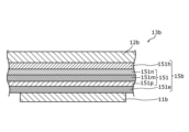
- FIG. 4 is a cross-sectional view schematically showing an exemplary cross-sectional structure of a pixel in the imaging device according to the embodiment.
- FIG. 5 is a schematic diagram showing the configuration of another imaging device according to the embodiment.
- FIG. 6 is a diagram showing an example of an absorption spectrum in a photoelectric conversion layer containing tin naphthalocyanine.
- 7A is a cross-sectional view schematically showing an example of a configuration of a photoelectric conversion layer in a first photoelectric conversion unit according to the embodiment
- FIG. 7B is a cross-sectional view schematically showing an example of a configuration of a photoelectric conversion layer in a second photoelectric conversion section according to the embodiment
- FIG. FIG. 8 is a graph showing exemplary photocurrent characteristics of the photoelectric conversion layer according to the embodiment.
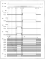
- FIG. 9 is a diagram for explaining operation example 1 of the imaging device according to the embodiment.
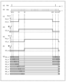
- FIG. 10 is a diagram for explaining Operation Example 2 of the imaging device according to the embodiment.
- FIG. 11 is a diagram for explaining a comparative example of the operation of the imaging device.
- FIG. 12 is a schematic diagram showing an exemplary circuit configuration of a pixel including a second photoelectric conversion unit and peripheral circuits in an imaging device according to a modification.
- FIG. 13 is a cross-sectional view schematically showing an exemplary cross-sectional structure of a pixel in an imaging device according to a modification.
- FIG. 14 is a diagram for explaining an operation example of an imaging device according to a modification;
- one photoelectric conversion unit when changing the voltage supplied to the photoelectric conversion units such as when trying to realize a global shutter function, one photoelectric conversion unit At least one of the one photoelectric conversion unit, the other photoelectric conversion unit, the signal detection circuit connected to the other photoelectric conversion unit, and the charge accumulation region connected to the other photoelectric conversion unit is changed by a change in the voltage supplied to the , the capacity of the charge storage region connected to the other photoelectric conversion portion fluctuates due to the capacitive coupling of the other photoelectric conversion portion, resulting in deterioration of image quality.
- the capacitance of the charge accumulation region fluctuates during the period in which signals are read out from the charge accumulation region and the period in which the potential of the charge accumulation region is reset, the image quality is significantly affected.
- the present disclosure has been made based on such findings.
- the other photoelectric conversion unit, a signal detection circuit connected to the other photoelectric conversion unit, and/or a charge storage region connected to the other photoelectric conversion unit Provides equipment and camera systems. Details are described below.
- An imaging device includes first pixels, second pixels, and a first voltage supply circuit.
- the first pixel includes a first photoelectric conversion unit that generates signal charges by photoelectric conversion, and a first signal detection circuit connected to the first photoelectric conversion unit.
- the second pixel includes a second photoelectric conversion unit stacked on the first photoelectric conversion unit to generate signal charges by photoelectric conversion, and a second signal detection circuit connected to the second photoelectric conversion unit. .
- the first voltage supply circuit supplies a voltage to the first photoelectric conversion section.
- the first photoelectric conversion section includes a first pixel electrode, a first counter electrode facing the first pixel electrode, and a first photoelectric conversion layer positioned between the first pixel electrode and the first counter electrode. and including.
- the voltage applied between the first pixel electrode and the first counter electrode by the first voltage supply circuit is the period of one frame period excluding the readout period and the reset period of the second photoelectric conversion unit. can be switched between multiple voltages.
- the first photoelectric conversion unit, the second photoelectric conversion unit, the second signal detection circuit, and the area for accumulating the signal charges generated by the second photoelectric conversion unit Capacitive coupling occurs between at least one of them.
- a change in capacity for accumulating signal charges generated by the second photoelectric conversion unit by not switching the voltage applied to the first photoelectric conversion unit during the readout period and the reset period of the second photoelectric conversion unit does not occur during the read and reset periods.
- the output signal of the second signal detection circuit does not fluctuate during the readout period and the reset period, and the signal charges generated by the first photoelectric conversion unit, the second photoelectric conversion unit, the second signal detection circuit, and the second photoelectric conversion unit image quality deterioration due to capacitive coupling with at least one of the areas for accumulating .
- the imaging device according to the second aspect of the present disclosure may be the imaging device according to the first aspect, and the first pixel and the second pixel may each be an effective pixel.
- an imaging device is the imaging device according to the first aspect or the second aspect, wherein the sensitivity of the first photoelectric conversion unit is the sensitivity of the first pixel electrode and the first pixel electrode.
- the voltage applied between the counter electrodes may be variable by switching between the plurality of voltages.
- the sensitivity at the time of imaging using the first photoelectric conversion unit can be adjusted only by switching the voltage to be applied.
- an imaging device is the imaging device according to the third aspect, wherein the first photoelectric conversion unit is provided between the first pixel electrode and the first counter electrode. It may be driven by a global shutter method in which an exposure period is defined by switching the applied voltage between the plurality of voltages.
- an imaging device is the imaging device according to the first or second aspect, and further includes a second voltage supply circuit that supplies voltage to the second photoelectric conversion unit.
- the second photoelectric conversion section includes a second pixel electrode, a second counter electrode facing the second pixel electrode, and a second photoelectric conversion layer positioned between the second pixel electrode and the second counter electrode. and may include The sensitivity of the second photoelectric conversion unit is variable by switching the voltage applied between the second pixel electrode and the second counter electrode by the second voltage supply circuit between a plurality of voltages. good too.
- the second photoelectric conversion unit employs a global shutter method in which an exposure period is defined by switching the voltage applied between the second pixel electrode and the second counter electrode between the plurality of voltages. You can drive.
- an imaging device is the imaging device according to any one of the first aspect to the fifth aspect, wherein during the exposure period of the second photoelectric conversion unit, An exposure period and a readout period for one photoelectric conversion unit may be included.
- the exposure period of the second photoelectric conversion unit can be lengthened without lengthening one frame period, and the sensitivity during imaging using the second photoelectric conversion unit can be increased.
- an imaging device is the imaging device according to any one of the first aspect to the sixth aspect, wherein during the exposure period of the second photoelectric conversion unit, The exposure period and readout period for one photoelectric conversion unit may be included in this order.
- the interval from the exposure period of the first photoelectric conversion unit to the readout period can be shortened. Therefore, for example, during imaging using the first photoelectric conversion unit, the influence of dark current can be reduced, and image quality deterioration can be suppressed. Further, for example, when capturing an image using the first photoelectric conversion unit, it is possible to suppress deterioration of image quality due to unintended parasitic sensitivity during a period other than the exposure period.
- an imaging device is the imaging device according to the seventh aspect, wherein the reset period of the first photoelectric conversion unit is set in the exposure period of the second photoelectric conversion unit, The exposure period and the readout period may be included in this order.
- the interval from the reset period of the first photoelectric conversion unit to the readout period can be shortened. Therefore, for example, during imaging using the first photoelectric conversion unit, the influence of dark current can be reduced, and image quality deterioration can be suppressed. Also, for example, when imaging using the first photoelectric conversion unit, it is possible to further suppress image quality deterioration due to unintended parasitic sensitivity during periods other than the exposure period.
- an imaging device is the imaging device according to any one of the first to eighth aspects, wherein the first photoelectric conversion unit and the second photoelectric conversion unit A stacked third photoelectric conversion unit and a third signal detection circuit connected to the third photoelectric conversion unit may be further provided.
- each photoelectric conversion unit has sensitivity in the wavelength regions of red, green, and blue, color images can be easily acquired.
- the imaging device further includes a fourth photoelectric conversion unit, if each photoelectric conversion unit has sensitivity in the wavelength regions of red, green, blue, and near-infrared rays, a color image and a near-infrared image can be easily obtained. can be obtained.
- an imaging device is the imaging device according to any one of the first to ninth aspects, wherein the first photoelectric conversion unit and the second photoelectric conversion unit One of them may have sensitivity in the near-infrared wavelength region, and the other of the first photoelectric conversion unit and the second photoelectric conversion unit may have sensitivity in the visible light wavelength region.
- a visible light image and a near-infrared image can be acquired with one imaging device.
- the imaging device according to the eleventh aspect of the present disclosure is the imaging device according to the tenth aspect, wherein the exposure period of the one of the first photoelectric conversion unit and the second photoelectric conversion unit is The exposure period may be shorter than the exposure period of the other of the first photoelectric conversion unit and the second photoelectric conversion unit.
- a photoelectric conversion part having sensitivity in the near-infrared wavelength region is likely to generate dark current due to thermal excitation because the bandgap of the photoelectric conversion material used is narrow.
- an imaging device is the imaging device according to any one of the first to eleventh aspects, wherein the second photoelectric conversion unit includes a silicon photodiode.
- a camera system includes an imaging device according to any one of the first to twelfth aspects, and at least one of the first photoelectric conversion section and the second photoelectric conversion section. and an illumination device that emits light including an emission peak in a wavelength range to which the is sensitive. The illumination device emits the light in a period overlapping with the exposure period of at least one of the first photoelectric conversion section and the second photoelectric conversion section.
- the image can be captured using the light emitted by the lighting device, so the image quality of the captured image can be improved.
- the terms “upper” and “lower” do not refer to the upward direction (vertically upward) and the downward direction (vertically downward) in absolute spatial recognition, but are based on the stacking order in the stacking structure. It is used as a term defined by a relative positional relationship. Specifically, the light-receiving side of the imaging device is defined as “upper”, and the side opposite to the light-receiving side is defined as “lower”. Note that terms such as “upper” and “lower” are used only to specify the mutual arrangement of members, and are not intended to limit the orientation of the imaging apparatus when it is used.
- the terms “above” and “below” are used not only when two components are spaced apart from each other and there is another component between the two components, but also when two components are spaced apart from each other. It also applies when two components are in contact with each other and are placed in close contact with each other.
- FIG. 1 is a block diagram showing an example of the functional configuration of the camera system according to this embodiment.
- the camera system 1 includes an imaging device 100, an illumination device 200, and a control section 300.
- illumination light 602 emitted by the illumination device 200 is reflected by the subject 600 .
- Reflected light 604 generated by the illumination light 602 being reflected by the object 600 is converted into electric charge by the photoelectric conversion unit of the imaging device 100 and extracted as an electric signal to be imaged.
- imaging device 100, lighting device 200, and control unit 300 are shown as separate functional blocks, but imaging device 100, lighting device 200, and control unit 300 Two or more may be integrated.
- imaging device 100 may include lighting device 200 .
- the imaging device 100 converts light incident on the camera system 1 into an electrical signal and outputs an image (image signal).
- the imaging device 100 includes a first photoelectric conversion unit 13a and a second photoelectric conversion unit 13b.
- Each of the first photoelectric conversion unit 13a and the second photoelectric conversion unit 13b is, for example, a photoelectric conversion element.
- illumination light specifically, reflected light generated by reflection of the illumination light emitted by the illumination device 200 on the subject enters the first photoelectric conversion unit 13a and the second photoelectric conversion unit 13b.
- the first photoelectric conversion unit 13a and the second photoelectric conversion unit 13b each generate signal charges through photoelectric conversion.
- a signal corresponding to the amount of signal charge generated by each of the first photoelectric conversion unit 13a and the second photoelectric conversion unit 13b is read out and output from the imaging device 100 as an image signal.
- the first photoelectric conversion unit 13a and the second photoelectric conversion unit 13b have sensitivities in different wavelength ranges.
- the first photoelectric conversion unit 13a has sensitivity in the first wavelength band.
- the second photoelectric conversion unit 13b has sensitivity in the second wavelength band.
- having sensitivity to a certain wavelength means having an external quantum efficiency of 1% or more at a certain wavelength.
- the illumination device 200 irradiates the subject with illumination light.
- the illumination device 200 emits, as illumination light, light having an emission peak in a wavelength range to which at least one of the first photoelectric conversion unit 13a and the second photoelectric conversion unit 13b is sensitive.
- the illumination device 200 has, for example, a first light source 210a and a second light source 210b.
- the first light source 210a emits light containing, for example, a component having a wavelength in at least part of the first wavelength band to which the first photoelectric conversion section 13a is sensitive.
- the first light source 210a emits light having an emission peak in, for example, the first wavelength band.
- the second light source 210b emits light containing, for example, a component having a wavelength in at least part of the second wavelength range to which the second photoelectric conversion section 13b is sensitive.
- the second light source 210b emits light having an emission peak in the second wavelength band, for example.
- the types of light sources used as the first light source 210a and the second light source 210b are not particularly limited as long as they can emit light of desired wavelengths.
- the first light source 210a and the second light source 210b are, for example, halogen light sources, LED (Light Emitting Diode) light sources, organic EL (Electro Luminescence) light sources, laser diode light sources, or the like.
- a plurality of light sources having different emission wavelengths may be used in combination for the first light source 210a and the second light source 210b.
- the first wavelength range and the second wavelength range are, for example, wavelength ranges included in any one of the ultraviolet wavelength range, the visible light wavelength range, and the near-infrared wavelength range.
- the first photoelectric conversion unit 13a may have sensitivity to wavelengths other than the first wavelength band.
- the second photoelectric conversion unit 13b may have sensitivity to wavelengths other than the second wavelength range.
- the first wavelength range is a wavelength range within the near-infrared wavelength range
- the second wavelength range is a wavelength range within the visible light wavelength range. Therefore, the first light source 210a emits light having an emission peak in the near-infrared wavelength region. Also, the second light source 210b emits light having an emission peak in the visible light wavelength region. In this case, the light emitted by the first light source 210a is converted by the first photoelectric converter 13a having sensitivity in the near-infrared wavelength region, extracted as an electric signal, and captured. Also, the light emitted by the second light source 210b is converted by the second photoelectric conversion unit 13b having sensitivity in the visible light wavelength region, extracted as an electric signal, and captured. This makes it possible to realize the imaging device 100 that separates and extracts signals corresponding to visible light and near-infrared light. Therefore, for example, a visible light image and a near-infrared image can be acquired.
- the near-infrared wavelength region refers to, for example, a wavelength region of 680 nm or more and 3000 nm or less.
- the near-infrared wavelength region may refer to a wavelength region of 700 nm or more and 2000 nm or less, or may refer to a wavelength region of 700 nm or more and 1600 nm or less.
- the visible light wavelength region refers to, for example, a wavelength region of 380 nm or more and less than 680 nm.
- the ultraviolet wavelength range refers to, for example, a wavelength range of 100 nm or more and less than 380 nm, and may refer to a wavelength range of 200 nm or more and less than 380 nm.
- all electromagnetic waves including visible light, infrared rays and ultraviolet rays are expressed as "light" for convenience.
- the first wavelength range may be a wavelength range within the ultraviolet wavelength range
- the second wavelength range may be a wavelength range within the visible light wavelength range. Accordingly, the imaging device 100 that separates and extracts signals corresponding to visible light and ultraviolet light can be realized. Therefore, for example, a visible light image and an ultraviolet image can be obtained.
- each of the first wavelength band and the second wavelength band may be a wavelength band within the near-infrared wavelength region. Accordingly, the imaging apparatus 100 that separates and extracts signals corresponding to near-infrared rays having different wavelengths can be realized. Therefore, for example, two types of near-infrared images with different wavelengths can be acquired. For example, by generating a difference image using such two types of near-infrared images, it is possible to obtain a near-infrared image in which the influence of absorption of ambient light or moisture is reduced.
- At least one of the first wavelength range and the second wavelength range is a wavelength range within the near-infrared wavelength range
- at least one may be a wavelength range within the range of 820 nm or more and 980 nm or less.
- an inexpensive LED light source having an emission peak at 820 nm or more and 980 nm or less can be used as the light source of the illumination device 200 that emits illumination light.
- the number of light sources included in the lighting device 200 is not limited to two, and may be one, or three or more.
- lighting device 200 may be configured to include only first light source 210a or second light source 210b as a light source.
- the first photoelectric conversion unit 13a or the second photoelectric conversion unit 13b converts ambient light or light from an external light source reflected by the subject into charges.
- the first light source 210a and the second light source 210b may not be provided in one lighting device, and the camera system 1 includes the lighting device having the first light source 210a and the lighting device having the second light source 210b. and may be provided.
- the camera system 1 may not include the illumination device 200 .
- the wavelength ranges of the first wavelength band and the second wavelength band exemplified above may be interchanged.
- the first wavelength range may be a wavelength range within the visible light wavelength range
- the second wavelength range may be a wavelength range within the near-infrared wavelength range.
- the control unit 300 is a control circuit that controls operations of the imaging device 100 and the lighting device 200 .
- the control unit 300 outputs various drive signals to the imaging device 100 and the lighting device 200, for example.
- Control unit 300 is realized by, for example, a microcomputer.
- the functions of the control unit 300 may be realized by a combination of a general-purpose processing circuit and software, or may be realized by hardware specialized for such processing.
- control unit 300 for example, the function of controlling the driving of the imaging device 100 may be included in the imaging device 100 .
- the control unit 300 may be provided in the imaging device 100 as a control circuit or the like. Therefore, the driving of the peripheral circuits and pixels of the imaging device 100 to be described later may be performed based on the control of the control unit 300 provided outside the imaging device 100 . It may be performed based on the control of the unit 300).
- FIG. 2 is a schematic diagram showing a schematic configuration of an imaging device according to this embodiment.
- FIG. 2 schematically shows a photoelectric conversion unit of each pixel of the imaging device 100 according to the present embodiment and a signal detection circuit connected thereto.
- the imaging device 100 includes a first photoelectric conversion unit 13a, a signal detection circuit 14a connected to the first photoelectric conversion unit 13a, a second photoelectric conversion unit 13b, and a second photoelectric conversion unit. 13b, and a semiconductor substrate 20 provided with the signal detection circuit 14a and the signal detection circuit 14b.
- the signal detection circuit 14a is an example of a first signal detection circuit.
- the signal detection circuit 14b is an example of a second signal detection circuit.
- FIG. 2 shows the first photoelectric conversion unit 13a and the second photoelectric conversion unit 13b for four pixels, respectively. is not particularly limited. Also, the number of pixels in the first photoelectric conversion unit 13a and the number of pixels in the second photoelectric conversion unit 13b may be the same or different. For example, FIG. 2 illustrates an example in which a four-pixel second photoelectric conversion unit 13b is stacked on a four-pixel first photoelectric conversion unit 13a. 4 pixels of the second photoelectric conversion unit 13b may be stacked.
- Both the first photoelectric conversion unit 13a and the second photoelectric conversion unit 13b may have sensitivity to at least one of visible light, near-infrared rays, infrared rays, and ultraviolet rays.
- a color filter in a Bayer array is provided above the second photoelectric conversion unit 13b having sensitivity in the entire visible light wavelength region, and each pixel provided in the second photoelectric conversion unit 13b is connected to the corresponding color filter. Accordingly, pixel signals corresponding to red, blue and green light intensities may be output.
- each pixel provided in the first photoelectric conversion unit 13a having sensitivity in the near-infrared wavelength region may output a pixel signal corresponding to the intensity of near-infrared rays. Thereby, a color image corresponding to the signal charge of the second photoelectric conversion unit 13b is obtained, and a near-infrared image corresponding to the signal charge of the first photoelectric conversion unit 13a is obtained.
- the signal detection circuit 14a and the signal detection circuit 14b are formed on the same plane on the semiconductor substrate 20 in the example shown in FIG.
- the signal detection circuits 14a and 14b may be formed side by side on the same plane on the semiconductor substrate 20 as shown in FIG. 2, or may be vertically divided and formed on different planes.
- FIG. 3A is a schematic diagram showing an exemplary circuit configuration of a pixel including a first photoelectric conversion unit and peripheral circuits in the imaging device according to the present embodiment.
- FIG. 3B is a schematic diagram showing an exemplary circuit configuration of a pixel including a second photoelectric conversion unit and peripheral circuits in the imaging device according to the present embodiment.
- the imaging device 100 includes a plurality of pixels including a plurality of pixels 10a and a plurality of pixels 10b, and peripheral circuits. More specifically, the imaging device 100 includes a pixel array PA including a plurality of two-dimensionally arranged pixels 10a and a plurality of two-dimensionally arranged pixels 10b, and a peripheral circuit.
- 3A and 3B schematically show examples in which the pixels 10a and the pixels 10b are arranged in a matrix of two rows and two columns, respectively.
- the first photoelectric conversion unit 13a and the signal detection circuit 14a constitute at least part of the pixel 10a
- the second photoelectric conversion unit 13b and the signal detection circuit 14b constitute at least part of the pixel 10b.
- the first photoelectric conversion unit 13a of the pixel 10a and the second photoelectric conversion unit 13b of the pixel 10b are stacked.
- the number and arrangement of pixels 10a and pixels 10b in imaging device 100 are not limited to the examples shown in FIGS. 3A and 3B.
- the pixel 10a is an example of a first pixel
- the pixel 10b is an example of a second pixel.
- the pixels 10a and 10b are, for example, effective pixels.
- effective pixels are pixels that are actually used for image output or pixels that are used during sensing, and do not include optical black pixels and dummy pixels that are used to measure dark noise.
- At least one of the pixels 10a and 10b may be an optical black pixel or a dummy pixel.
- the peripheral circuit drives the pixel array PA and acquires an image based on signal charges generated by the first photoelectric conversion unit 13a and the second photoelectric conversion unit 13b.
- the peripheral circuits include, for example, a voltage supply circuit 32a connected to the pixels 10a, a reset voltage source 34a, a vertical scanning circuit 36a, a column signal processing circuit 37a, a horizontal signal readout circuit 38a, and a voltage source connected to the power line 40a.
- the peripheral circuits include, for example, a voltage supply circuit 32b connected to the pixel 10b, a reset voltage source 34b, a vertical scanning circuit 36b, a column signal processing circuit 37b, a horizontal signal readout circuit 38b, and a voltage source connected to the power supply line 40b.
- the imaging apparatus 100 may include a control circuit that controls driving of peripheral circuits other than itself as a circuit included in the peripheral circuits.
- the pixel 10a shown in FIG. 3A and the peripheral circuit connected to the pixel 10a and the pixel 10b shown in FIG. 3B and the peripheral circuit connected to the pixel 10b have, for example, functionally similar circuit configurations.
- a circuit configuration of the pixel 10a having the first photoelectric conversion unit 13a and the pixel 10b having the second photoelectric conversion unit 13b will be described with reference to FIGS. 3A and 3B.
- Each pixel 10a has a first photoelectric conversion unit 13a and a signal detection circuit 14a.
- Each pixel 10b has a second photoelectric conversion unit 13b and a signal detection circuit 14b.
- each of the first photoelectric conversion unit 13a and the second photoelectric conversion unit 13b has a photoelectric conversion layer sandwiched between two electrodes facing each other, and converts incident light into receive and generate signal charges.
- the entire first photoelectric conversion unit 13a does not need to be an independent element for each pixel 10a.
- a portion of the first photoelectric conversion unit 13a may extend over a plurality of pixels 10a.
- the second photoelectric conversion unit 13b does not need to be an independent element for each pixel 10b as a whole.
- the signal detection circuit 14a is a circuit that detects signal charges generated by the first photoelectric conversion unit 13a.
- the signal detection circuit 14b is a circuit that detects signal charges generated by the second photoelectric conversion unit 13b.
- the signal detection circuit 14a includes a signal detection transistor 24a and an address transistor 26a.
- the signal detection circuit 14b also includes a signal detection transistor 24b and an address transistor 26b.
- Signal detection transistors 24a and 24b and address transistors 26a and 26b are, for example, field effect transistors (FETs), respectively, where N-channel MOSFETs (Metal Oxide Semiconductor Field Effect Transistor).
- Each transistor such as signal detection transistors 24a and 24b, address transistors 26a and 26b, and reset transistors 28a and 28b to be described later, has a control terminal, an input terminal and an output terminal.
- a control terminal is, for example, a gate.
- the input terminal is one of the drain and the source, for example the drain.
- the output terminal is the other of the drain and the source, for example the source.
- the control terminal of the signal detection transistor 24a has an electrical connection with the first photoelectric conversion section 13a.
- the signal charge generated by the first photoelectric conversion unit 13a is accumulated in a region including the charge accumulation node 41a between the gate of the signal detection transistor 24a and the first photoelectric conversion unit 13a.
- the control terminal of the signal detection transistor 24b is electrically connected to the second photoelectric conversion section 13b.
- the signal charges generated by the second photoelectric conversion unit 13b are accumulated in a region including the charge accumulation node 41b between the gate of the signal detection transistor 24b and the second photoelectric conversion unit 13b.
- the signal charges are holes or electrons.
- a charge storage node is at least part of a charge storage region that stores signal charge, and is also called a “floating diffusion node”. The details of the structures of the first photoelectric conversion unit 13a and the second photoelectric conversion unit 13b will be described later.
- the first photoelectric conversion unit 13a of each pixel 10a further has a connection with the sensitivity control line 42a.
- the sensitivity control line 42a is connected to the voltage supply circuit 32a.
- the second photoelectric conversion unit 13b of each pixel 10b is further connected to a sensitivity control line 42b.
- the sensitivity control line 42b is connected to the voltage supply circuit 32b.
- the voltage supply circuit is also called a sensitivity control electrode supply circuit.
- Each of the voltage supply circuits 32a and 32b is a circuit capable of supplying at least two voltages.
- the voltage supply circuit 32a is an example of a first voltage supply circuit that supplies voltage to the first photoelectric conversion unit 13a. Specifically, the voltage supply circuit 32a supplies a predetermined voltage to the first photoelectric conversion unit 13a through the sensitivity control line 42a when the imaging device 100 operates. Also, the voltage supply circuit 32b is an example of a second voltage supply circuit that supplies voltage to the second photoelectric conversion unit 13b. Specifically, the voltage supply circuit 32b supplies a predetermined voltage to the second photoelectric conversion section 13b through the sensitivity control line 42b when the imaging device 100 operates.
- the voltage supply circuits 32a and 32b are not limited to a specific power supply circuit, and may be a circuit that generates a predetermined voltage, or a circuit that converts a voltage supplied from another power source into a predetermined voltage. good too.
- the voltage supplied from the voltage supply circuit 32a to the first photoelectric conversion unit 13a is switched between a plurality of voltages different from each other, whereby the charge storage node 41a from the first photoelectric conversion unit 13a is controlled to start and end the accumulation of signal charges in the .
- the voltage supplied from the voltage supply circuit 32b to the second photoelectric conversion unit 13b is switched between a plurality of voltages different from each other. Start and end of accumulation is controlled.
- the electronic shutter by switching the voltage supplied from the voltage supply circuit 32a to the first photoelectric conversion unit 13a and the voltage supplied from the voltage supply circuit 32b to the second photoelectric conversion unit 13b, the electronic shutter is switched. Action is performed. An example of the operation of the imaging device 100 will be described later.
- Each pixel 10a is connected to a power supply line 40a that supplies power supply voltage VDD.
- Each pixel 10b has a connection with a power supply line 40b that supplies a power supply voltage VDD.
- the input terminal of the signal detection transistor 24a is connected to the power line 40a. Since the power line 40a functions as a source follower power supply, the signal detection transistor 24a amplifies and outputs the signal generated by the first photoelectric conversion section 13a.
- the input terminal of the signal detection transistor 24b is connected to the power line 40b. Since the power line 40b functions as a source follower power supply, the signal detection transistor 24b amplifies and outputs the signal generated by the second photoelectric conversion section 13b.
- the input terminal of the address transistor 26a is connected to the output terminal of the signal detection transistor 24a.
- the output terminal of the address transistor 26a is connected to one of a plurality of vertical signal lines 47a arranged for each column of pixels 10a in the pixel array PA.
- the control terminal of the address transistor 26a is connected to the address control line 46a, and by controlling the potential of the address control line 46a, the output of the signal detection transistor 24a can be selectively read out to the corresponding vertical signal line 47a. can be done.
- the input terminal of the address transistor 26b is connected to the output terminal of the signal detection transistor 24b.
- the output terminal of the address transistor 26b is connected to one of a plurality of vertical signal lines 47b arranged for each column of pixels 10b in the pixel array PA.
- the control terminal of the address transistor 26b is connected to the address control line 46b, and by controlling the potential of the address control line 46b, the output of the signal detection transistor 24b can be selectively read out to the corresponding vertical signal line 47b. can be done.
- the address control line 46a is connected to the vertical scanning circuit 36a. Also, in the example shown in FIG. 3B, the address control line 46b is connected to the vertical scanning circuit 36b.
- the vertical scanning circuit is also called "row scanning circuit".
- the vertical scanning circuit 36a selects a plurality of pixels 10a arranged in each row by applying a predetermined voltage to the address control line 46a.
- the vertical scanning circuit 36b applies a predetermined voltage to the address control line 46b to select the plurality of pixels 10b arranged in each row on a row-by-row basis.
- the vertical signal line 47a is a main signal line that transmits pixel signals from the plurality of pixels 10a of the pixel array PA to peripheral circuits.
- a column signal processing circuit 37a is connected to the vertical signal line 47a.
- the vertical signal line 47b is a main signal line that transmits pixel signals from the plurality of pixels 10b of the pixel array PA to peripheral circuits.
- a column signal processing circuit 37b is connected to the vertical signal line 47b.
- the column signal processing circuit is also called "row signal storage circuit”.
- the column signal processing circuits 37a and 37b respectively perform noise suppression signal processing typified by correlated double sampling, analog-to-digital conversion (AD conversion), and the like. As shown in FIG.
- a column signal processing circuit 37a is provided corresponding to each column of pixels 10a in the pixel array PA.
- a horizontal signal readout circuit 38a is connected to these column signal processing circuits 37a.
- the column signal processing circuit 37b is provided corresponding to each column of the pixels 10b in the pixel array PA.
- a horizontal signal readout circuit 38b is connected to these column signal processing circuits 37b.
- the horizontal signal readout circuit is also called a "column scanning circuit".
- the horizontal signal readout circuit 38a sequentially reads signals from the plurality of column signal processing circuits 37a to the horizontal common signal line 49a. Further, the horizontal signal readout circuit 38b sequentially reads signals from the plurality of column signal processing circuits 37b to the horizontal common signal line 49b.
- the pixel 10a has a reset transistor 28a.
- the pixel 10b has a reset transistor 28b.
- Reset transistors 28a and 28b can be, for example, field effect transistors, as can signal detection transistors 24a and 24b and address transistors 26a and 26b, respectively.
- N-channel MOSFETs are used as the reset transistors 28a and 28b will be described below unless otherwise specified.
- the reset transistor 28a is connected between the reset voltage line 44a that supplies the reset voltage Vr and the charge storage node 41a.
- a control terminal of the reset transistor 28a is connected to a reset control line 48a, and the potential of the charge storage node 41a can be reset to the reset voltage Vr by controlling the potential of the reset control line 48a.
- the reset control line 48a is connected to the vertical scanning circuit 36a. Therefore, when the vertical scanning circuit 36a applies a predetermined voltage to the reset control line 48a, the plurality of pixels 10a arranged in each row can be reset row by row.
- reset transistor 28b is connected between reset voltage line 44b that supplies reset voltage Vr and charge storage node 41b.
- a control terminal of the reset transistor 28b is connected to a reset control line 48b, and the potential of the charge storage node 41b can be reset to the reset voltage Vr by controlling the potential of the reset control line 48b.
- the reset control line 48b is connected to the vertical scanning circuit 36b. Therefore, when the vertical scanning circuit 36b applies a predetermined voltage to the reset control line 48b, it is possible to reset the plurality of pixels 10b arranged in each row on a row-by-row basis.
- a reset voltage line 44a that supplies a reset voltage Vr to the reset transistor 28a is connected to the reset voltage source 34a.
- a reset voltage line 44b for supplying a reset voltage Vr to the reset transistor 28b is connected to the reset voltage source 34b.
- a reset voltage source is also called a "reset voltage supply circuit".
- the reset voltage sources 34a and 34b only need to have a configuration capable of supplying a predetermined reset voltage Vr to the reset voltage lines 44a and 44b during operation of the imaging device 100, similarly to the voltage supply circuits 32a and 32b described above. , is not limited to any particular power supply circuit.
- Each of voltage supply circuits 32a and 32b and reset voltage sources 34a and 34b may be part of a single voltage supply circuit or may be independent and separate voltage supply circuits.
- One or both of the voltage supply circuit 32a and the reset voltage source 34a may be part of the vertical scanning circuit 36a.
- the sensitivity control voltage from the voltage supply circuit 32a and/or the reset voltage Vr from the reset voltage source 34a may be supplied to each pixel 10a via the vertical scanning circuit 36a.
- one or both of the voltage supply circuit 32b and the reset voltage source 34b may be part of the vertical scanning circuit 36b.
- the sensitivity control voltage from the voltage supply circuit 32b and/or the reset voltage Vr from the reset voltage source 34b may be supplied to each pixel 10b via the vertical scanning circuit 36b.
- the power supply voltage VDD of the signal detection circuits 14a and 14b can be used as the reset voltage Vr.
- a voltage supply circuit (not shown in FIG. 3A) that supplies a power supply voltage to each pixel 10a and the reset voltage source 34a can be shared.
- the power supply line 40a and the reset voltage line 44a can be shared, the wiring in the pixel array PA can be simplified.
- a voltage supply circuit (not shown in FIG. 3B) that supplies a power supply voltage to each pixel 10b and the reset voltage source 34b can be shared.
- the power supply line 40b and the reset voltage line 44b can be shared, the wiring in the pixel array PA can be simplified.
- using different voltages for the reset voltage Vr and the power supply voltage VDD of the signal detection circuits 14a and 14b enables more flexible control of the imaging device 100.
- FIG. 4 is a cross-sectional view schematically showing an exemplary cross-sectional structure of pixels 10a and 10b according to the present embodiment.
- the above-described signal detection transistors 24a and 24b, address transistors 26a and 26b and reset transistors 28a and 28b are formed on semiconductor substrate 20.
- the semiconductor substrate 20 is not limited to a substrate whose entirety is a semiconductor.
- the semiconductor substrate 20 may be an insulating substrate or the like having a semiconductor layer provided on the surface on which the photosensitive region is formed.
- the semiconductor substrate 20 has a plurality of semiconductor layers, and the signal detection transistor 24a, the address transistor 26a and the reset transistor 28a and the signal detection transistor 24b, the address transistor 26b and the reset transistor 28b are formed in different semiconductor layers.
- the signal detection transistor 24a, the address transistor 26a and the reset transistor 28a and the signal detection transistor 24b, the address transistor 26b and the reset transistor 28b are formed in different semiconductor layers.
- Si P-type silicon
- FIG. 4 an example in which the first photoelectric conversion section 13a and the second photoelectric conversion section 13b having the same size are arranged in the same region of the semiconductor substrate 20 in plan view will be described.
- the semiconductor substrate 20 has impurity regions 26s, 24s, 24d, 28d and 28s, and an isolation region 20t for electrical isolation between pixels.
- impurity regions 26s, 24s, 24d, 28d and 28s are N-type regions.
- the element isolation region 20t is also provided between the impurity regions 24d and 28d.
- the element isolation region 20t is formed, for example, by implanting acceptor ions under predetermined implantation conditions.
- the impurity regions 26s, 24s, 24d, 28d and 28s are diffusion layers formed in the semiconductor substrate 20, for example.
- signal detection transistors 24a and 24b each include impurity regions 24s and 24d and a gate electrode 24g.
- Gate electrode 24g is formed using a conductive material.
- the conductive material is, for example, polysilicon imparted with conductivity by being doped with impurities, but may also be a metal material.
- the impurity region 24s functions as, for example, source regions of the signal detection transistors 24a and 24b.
- the impurity region 24d functions as, for example, drain regions of the signal detection transistors 24a and 24b. Channel regions of signal detection transistors 24a and 24b are formed between impurity regions 24s and 24d.
- the address transistors 26a and 26b each include impurity regions 26s and 24s and a gate electrode 26g connected to an address control line 46a or 46b (see FIGS. 3A and 3B) not shown in FIG.
- Gate electrode 26g is formed using a conductive material.
- the conductive material is, for example, polysilicon imparted with conductivity by being doped with impurities, but may also be a metal material.
- signal detection transistor 24a and address transistor 26a are electrically connected to each other by sharing impurity region 24s.
- signal detection transistor 24b and address transistor 26b are electrically connected to each other by sharing impurity region 24s.
- Impurity region 26s functions as, for example, source regions of address transistors 26a and 26b.
- Impurity region 26s is connected to vertical signal line 47a or 47b (see FIGS. 3A and 3B) not shown in FIG.
- the reset transistors 28a and 28b respectively include impurity regions 28d and 28s and a gate electrode 28g connected to a reset control line 48a or 48b (see FIGS. 3A and 3B) not shown in FIG.
- the gate electrode 28g is formed using, for example, a conductive material.
- the conductive material is, for example, polysilicon imparted with conductivity by being doped with impurities, but may also be a metal material.
- the impurity region 28s functions as, for example, source regions of the reset transistors 28a and 28b.
- Impurity region 28s is connected to reset voltage line 44a or 44b (see FIGS. 3A and 3B) not shown in FIG.
- Impurity region 28d functions as, for example, a drain region of reset transistors 28a and 28b.
- An interlayer insulating layer 50 is arranged on the semiconductor substrate 20 so as to cover the signal detection transistors 24a and 24b, the address transistors 26a and 26b, and the reset transistors 28a and 28b.
- the interlayer insulating layer 50 is made of, for example, an insulating material such as silicon oxide.
- wiring layers 56 a and 56 b may be arranged in the interlayer insulating layer 50 .
- the wiring layers 56a and 56b are made of metal such as copper, for example.
- the wiring layer 56a may include wiring such as the above vertical signal line 47a in part thereof, for example.
- the wiring layer 56b may include wiring such as the above vertical signal line 47b in part thereof, for example.
- the number of insulating layers in interlayer insulating layer 50 and the number of layers included in wiring layers 56a and 56b arranged in interlayer insulating layer 50 can be set arbitrarily, and are not limited to the example shown in FIG.
- the first photoelectric conversion section 13a and the second photoelectric conversion section 13b are arranged on the interlayer insulating layer 50.
- the plurality of pixels 10a and the plurality of pixels 10b that constitute the pixel array PA are formed in and on the semiconductor substrate 20.
- a plurality of pixels 10a and pixels 10b arranged two-dimensionally on the semiconductor substrate 20 form a photosensitive region.
- the photosensitive area is also called the "pixel area”.
- the distance between two adjacent pixels 10a and the distance between two adjacent pixels 10b can each be approximately 2 ⁇ m, for example.
- the distance between two adjacent pixels is also called "pixel pitch”.
- the first photoelectric conversion unit 13a and the second photoelectric conversion unit 13b are supplied with light from above the first photoelectric conversion unit 13a and the second photoelectric conversion unit 13b, in other words, from the side opposite to the semiconductor substrate 20 side. Light enters from the side.
- the first photoelectric conversion portion 13a is an example of a pixel electrode 11a, which is an example of a first pixel electrode, a counter electrode 12a, which is an example of a first counter electrode, and a first photoelectric conversion layer disposed between them. and a photoelectric conversion layer 15a.
- the counter electrode 12a and the photoelectric conversion layer 15a are formed across a plurality of pixels 10a.
- the pixel electrode 11a is provided for each pixel 10a, and is electrically isolated from the pixel electrode 11a of the other pixel 10a by being spatially separated from the pixel electrode 11a of the other adjacent pixel 10a. ing.
- the second photoelectric conversion portion 13b is an example of a pixel electrode 11b, which is an example of a second pixel electrode, a counter electrode 12b, which is an example of a second counter electrode, and a second photoelectric conversion layer arranged between them. and a photoelectric conversion layer 15b.
- the counter electrode 12b and the photoelectric conversion layer 15b are formed across a plurality of pixels 10b.
- the pixel electrode 11b is provided for each pixel 10b, and is electrically separated from the pixel electrode 11b of the other pixel 10b by being spatially separated from the pixel electrode 11b of the other adjacent pixel 10b. ing.
- the second photoelectric conversion section 13b is stacked above the first photoelectric conversion section 13a with an insulating layer 62 interposed therebetween. Light transmitted through the second photoelectric conversion unit 13b and the insulating layer 62 is incident on the first photoelectric conversion unit 13a.
- the second photoelectric conversion unit 13b and the insulating layer 62 transmit at least part of the light of the wavelength to which the first photoelectric conversion unit 13a is sensitive.
- the first photoelectric conversion unit 13a and the second photoelectric conversion unit 13b are electrically insulated by the insulating layer 62, but the voltage applied to one of the first photoelectric conversion unit 13a and the second photoelectric conversion unit 13b is If it changes, it affects the capacitance of the charge storage region connected to the other photoelectric conversion portion due to capacitive coupling.
- switching of the voltage applied by the voltage supply circuit 32a to the first photoelectric conversion unit 13a and switching of the voltage applied by the voltage supply circuit 32b to the second photoelectric conversion unit 13b are performed at appropriate timings. It is possible to suppress deterioration in image quality due to the influence of such capacitive coupling. Details of the operation of the imaging device 100 will be described later.
- a sealing layer, a color filter, a microlens, and the like may be further provided above the second photoelectric conversion unit 13b.
- the pixel electrode 11a is an electrode for reading out signal charges generated by the first photoelectric conversion unit 13a. At least one pixel electrode 11a exists for each pixel 10a. The pixel electrode 11a is electrically connected to the gate electrode 24g and the impurity region 28d of the signal detection transistor 24a. The pixel electrode 11b is an electrode for reading signal charges generated by the second photoelectric conversion unit 13b. At least one pixel electrode 11b exists for each pixel 10b. The pixel electrode 11b is electrically connected to the gate electrode 24g and the impurity region 28d of the signal detection transistor 24b. Also, the pixel electrode 11b is arranged on the first photoelectric conversion section 13a side of the photoelectric conversion layer 15b.
- the counter electrode 12a is arranged to face the pixel electrode 11a with the photoelectric conversion layer 15a interposed therebetween.
- the counter electrode 12a is arranged, for example, on the side of the photoelectric conversion layer 15a on which light is incident. Therefore, the light transmitted through the counter electrode 12a is incident on the photoelectric conversion layer 15a.
- the counter electrode 12a is arranged, for example, on the second photoelectric conversion section 13b side of the photoelectric conversion layer 15a. Therefore, the first photoelectric conversion section 13a and the second photoelectric conversion section 13b are stacked such that the counter electrode 12a faces the pixel electrode 11b.
- the counter electrode 12a and the pixel electrode 11b are adjacent to each other with the insulating layer 62 interposed therebetween.
- the counter electrode 12b is arranged to face the pixel electrode 11b with the photoelectric conversion layer 15b interposed therebetween.
- the counter electrode 12b is arranged, for example, on the side of the photoelectric conversion layer 15b on which light is incident. Therefore, the light transmitted through the counter electrode 12b is incident on the photoelectric conversion layer 15b.
- the pixel electrode 11b, the counter electrode 12a, and the counter electrode 12b are each transparent electrodes made of, for example, a transparent conductive material.
- Transparent as used herein means transmitting at least a portion of light in the wavelength range to be detected, and does not necessarily transmit light over the entire wavelength range of visible light.
- the counter electrode 12b transmits at least part of the light of the wavelength to which the first photoelectric conversion section 13a is sensitive and at least part of the light of the wavelength to which the second photoelectric conversion section 13b is sensitive.
- the pixel electrode 11b and the counter electrode 12a transmit at least part of the light of the wavelength to which the first photoelectric conversion unit 13a is sensitive.
- Transparent conducting oxides such as ITO, IZO, AZO, FTO, SnO 2 , TiO 2 and ZnO 2 can be used for the transparent electrode.
- the pixel electrode 11a is formed using a conductive material.
- the conductive material is, for example, a metal such as aluminum or copper, a metal nitride, or polysilicon that is doped with impurities to make it conductive.
- the pixel electrode 11a may be a light shielding electrode.
- a TaN electrode with a thickness of 100 nm as the pixel electrode 11a
- a sufficient light shielding property can be realized.
- channels of transistors in this example, at least one of the signal detection transistors 24a and 24b, the address transistors 26a and 26b, and the reset transistors 28a and 28b
- a light shielding film may be formed in the interlayer insulating layer 50 using the wiring layers 56a and 56b described above.
- the pixel electrode 11a may be a transparent electrode.
- the pixel electrode 11a and the counter electrode 12a may be arranged with their positions reversed from the arrangement shown in FIG. In this case, if the pixel electrode 11a is a transparent electrode and the counter electrode 12a is formed using a conductive material, it may not be a transparent electrode. Moreover, in this case, the plug 52a is arranged so as to penetrate the counter electrode 12a and the photoelectric conversion layer 15a.
- the pixel electrode 11b and the counter electrode 12b may be arranged with their positions reversed from the arrangement shown in FIG.
- the plug 52b is arranged so as to penetrate the counter electrode 12b and the photoelectric conversion layer 15b as well.
- first photoelectric conversion unit 13a and the second photoelectric conversion unit 13b may be arranged with their positions reversed from the arrangement shown in FIG.
- the photoelectric conversion layers 15a and 15b each receive incident light and generate hole-electron pairs.
- Photoelectric conversion layers 15a and 15b are each made of, for example, an organic material.
- each of the photoelectric conversion layers 15a and 15b may have a structure in which a plurality of layers are laminated. Specific examples of the materials forming the photoelectric conversion layers 15a and 15b will be described later.
- the counter electrode 12a has a connection with the sensitivity control line 42a connected to the voltage supply circuit 32a. Also, here, the counter electrode 12a is formed across a plurality of pixels 10a. Therefore, it is possible to collectively apply a desired magnitude of sensitivity control voltage from the voltage supply circuit 32a to the plurality of pixels 10a via the sensitivity control line 42a. Also, as described with reference to FIG. 3B, the counter electrode 12b has a connection with the sensitivity control line 42b connected to the voltage supply circuit 32b. Also, here, the counter electrode 12b is formed across a plurality of pixels 10b.
- At least one of the counter electrodes 12a and 12b may be provided separately for each pixel 10a or 10b as long as a desired sensitivity control voltage can be applied from the voltage supply circuit 32a or 32b.
- at least one of the photoelectric conversion layers 15a and 15b may be separately provided for each pixel 10a or 10b.
- the voltage supply circuits 32a and 32b respectively supply different voltages to the counter electrode 12a or 12b between the exposure period and the non-exposure period.
- the “exposure period” refers to accumulation of one of positive and negative charges (signal charge) generated by photoelectric conversion of the first photoelectric conversion unit 13a and the second photoelectric conversion unit 13b in a charge accumulation region or the like. , and may be called a "charge accumulation period”.
- non-exposure period a period other than the exposure period during which the imaging apparatus is in operation.
- the “non-exposure period” is not limited to the period during which light is blocked from entering the first photoelectric conversion unit 13a or the second photoelectric conversion unit 13b. A period during which light is applied to 13b may be included.
- the “non-exposure period” includes a period during which signal charges are unintentionally accumulated in the charge accumulation region due to the occurrence of parasitic sensitivity.
- the "non-exposure period” includes the “readout period” and the “reset period”.
- the “readout period” signals corresponding to the amount of signal charges generated by the first photoelectric conversion unit 13a and the second photoelectric conversion unit 13b (that is, the amount of signal charge accumulated in the charge accumulation region) are detected by signal detection circuits. 14a and 14b are readout periods.
- the “reset period” is a period for resetting the potential of the charge accumulation region that accumulates signal charges generated by the first photoelectric conversion unit 13a and the second photoelectric conversion unit 13b. Specifically, in the "reset period", the potential of the charge accumulation region is reset to the reset voltage Vr.
- an "exposure period”, a “non-exposure period”, a “readout period” and a “reset period” are defined for each of the pixels 10a and 10b.
- a signal corresponding to the amount of signal charge generated by the first photoelectric conversion unit 13a is read out. It can also be said that they are the “exposure period”, the “non-exposure period”, the “readout period” and the “reset period” of the first photoelectric conversion unit 13a.
- the "exposure period”, “non-exposure period”, “readout period” and “reset period” of the pixel 10b are set. can also be said to be the “exposure period”, the “non-exposure period”, the “readout period” and the “reset period” of the second photoelectric conversion unit 13b. Details of each period will be described later.
- one of the hole-electron pairs generated in the photoelectric conversion layer 15a by photoelectric conversion is used as a signal charge in the pixel. It can be collected by electrode 11a.
- holes can be selectively collected by the pixel electrode 11a by making the potential of the counter electrode 12a higher than that of the pixel electrode 11a.
- the potential of the counter electrode 12b with respect to the potential of the pixel electrode 11b, either holes or electrons of the hole-electron pairs generated in the photoelectric conversion layer 15b by photoelectric conversion are converted into signal charges. can be collected by the pixel electrode 11b as .
- holes can be selectively collected by the pixel electrode 11b by making the potential of the counter electrode 12b higher than that of the pixel electrode 11b.
- a case where holes are used as signal charges will be exemplified below.
- electrons can also be used as signal charges.
- the potential of the counter electrode 12a is set lower than that of the pixel electrode 11a
- the potential of the counter electrode 12b is set lower than that of the pixel electrode 11b.
- the pixel electrode 11a opposed to the counter electrode 12a receives positive and negative charges generated by photoelectric conversion in the photoelectric conversion layer 15a. Collect one.
- the pixel electrode 11b facing the counter electrode 12b is applied with an appropriate bias voltage between the counter electrode 12b and the pixel electrode 11b, so that the positive and negative charges generated by photoelectric conversion in the photoelectric conversion layer 15b are removed. Collect one of them.
- the imaging device 100 is provided with an insulating layer 62 arranged between the first photoelectric conversion section 13a and the second photoelectric conversion section 13b.
- the insulating layer 62 electrically separates the first photoelectric conversion section 13a and the second photoelectric conversion section 13b.
- a pixel electrode 11a, a photoelectric conversion layer 15a, a counter electrode 12a, an insulating layer 62, a pixel electrode 11b, a photoelectric conversion layer 15b, and a counter electrode 12b are stacked in this order from the bottom side.
- the insulating layer 62 is made of a transparent insulating material.
- the insulating layer 62 transmits at least part of light having a wavelength to which the first photoelectric conversion unit 13a is sensitive. Silicon oxynitride, aluminum oxide, or the like, for example, can be used for the insulating layer 62 .
- the pixel electrode 11a is connected to the gate electrode 24g of the signal detection transistor 24a via the plug 52a, the wiring 53a and the contact plug 54a.
- the gate of the signal detection transistor 24a has an electrical connection with the pixel electrode 11a.
- the plug 52a, the wiring 53a, and the contact plug 54a constitute at least part of the charge storage node 41a (see FIG. 3A) between the signal detection transistor 24a and the first photoelectric conversion section 13a.
- the wiring 53a can be part of the wiring layer 56a.
- the pixel electrode 11a is also connected to the impurity region 28d of the reset transistor 28a through the plug 52a, the wiring 53a and the contact plug 55a. In the configuration illustrated in FIG.
- the gate electrode 24g of the signal detection transistor 24a, the plug 52a, the wiring 53a, the contact plugs 54a and 55a, and the impurity region 28d, which is one of the source and drain regions of the reset transistor 28a, form the pixel. It functions as a charge storage region of the pixel 10a that stores the signal charge collected by the electrode 11a.
- the pixel electrode 11b is connected to the gate electrode 24g of the signal detection transistor 24b via the plug 52b, the wiring 53b and the contact plug 54b.
- the gate of the signal detection transistor 24b has an electrical connection with the pixel electrode 11b.
- the plug 52b penetrates through the first photoelectric conversion section 13a and the insulating layer 62 .
- the plug 52b, the wiring 53b, and the contact plug 54b constitute at least part of the charge storage node 41b (see FIG. 3B) between the signal detection transistor 24b and the second photoelectric conversion section 13b.
- the wiring 53b can be part of the wiring layer 56b.
- the pixel electrode 11b is also connected to the impurity region 28d of the reset transistor 28b through the plug 52b, wiring 53b and contact plug 55b.
- the gate electrode 24g of the signal detection transistor 24b, the plug 52b, the wiring 53b, the contact plugs 54b and 55b, and the impurity region 28d which is one of the source and drain regions of the reset transistor 28b, form the pixel. It functions as a charge storage region of the pixel 10b that stores the signal charge collected by the electrode 11b.
- Plugs 52a and 52b, wirings 53a and 53b, and contact plugs 54a, 54b, 55a and 55b are each formed using a conductive material.
- plugs 52a and 52b and wires 53a and 53b are each made of metal such as copper.
- each of the contact plugs 54a, 54b, 55a and 55b is made of polysilicon to which conductivity is imparted by being doped with impurities.
- Plugs 52a and 52b, interconnections 53a and 53b, and contact plugs 54a, 54b, 55a and 55b may be formed using the same material or different materials.
- an insulating coating 61b is formed around the plug 52b.
- the insulating coating 61b is located between the plug 52b and the first photoelectric conversion part 13a.
- the plug 52b and the first photoelectric conversion portion 13a are not in contact with each other and are electrically insulated by the insulating coating 61b.
- the insulating coating 61b is formed using an insulating material such as silicon oxide or silicon nitride, for example.
- a voltage corresponding to the amount of signal charge accumulated in the charge accumulation region of the pixel 10a is applied to the gate of the signal detection transistor 24a.
- Signal detection transistor 24a amplifies this voltage.
- the voltage amplified by the signal detection transistor 24a is selectively read out as a signal voltage through the address transistor 26a.
- a voltage corresponding to the amount of signal charges accumulated in the charge accumulation region of the pixel 10b is applied to the gate of the signal detection transistor 24b.
- Signal detection transistor 24b amplifies this voltage.
- the voltage amplified by the signal detection transistor 24b is selectively read out as a signal voltage through the address transistor 26b.
- FIG. 5 is a schematic diagram showing the configuration of another imaging device according to this embodiment.
- FIG. 5 schematically shows a photoelectric conversion section and a signal detection circuit included in the imaging device, and omits illustration of other configurations.
- FIG. 5 illustrates the pixel structure above the upper end of the interlayer insulating layer 50 and the connection between the photoelectric conversion section and the signal detection circuit.
- the imaging device 110 differs from the imaging device 100 mainly in that it further includes photoelectric conversion units 13c and 13d and signal detection circuits 14c and 14d.
- the imaging device 110 includes reset transistors for resetting the photoelectric conversion units 13c and 13d, and the photoelectric conversion unit 13c, similarly to the imaging device 100 described with reference to FIGS. 3A to 4 . and a peripheral circuit for acquiring an image based on the signal charges generated in 13d.
- the photoelectric conversion units 13c and 13d are examples of a third photoelectric conversion unit.
- Signal detection circuits 14c and 14d are an example of a third signal detection circuit.
- the photoelectric conversion unit 13c and the signal detection circuit 14c may form part of the pixel 10a or the pixel 10b, or may form at least part of a pixel different from the pixel 10a and the pixel 10b. Further, the photoelectric conversion unit 13d and the signal detection circuit 14d may constitute a part of the pixel 10a or the pixel 10b, or may constitute at least part of a pixel different from the pixel 10a and the pixel 10b. .
- the photoelectric conversion units 13c and 13d are stacked above the first photoelectric conversion unit 13a and the second photoelectric conversion unit 13b. Specifically, in the imaging device 110, the first photoelectric conversion unit 13a, the second photoelectric conversion unit 13b, the photoelectric conversion unit 13c, and the photoelectric conversion unit 13d are stacked in this order from the lower side. Note that the stacking order of the photoelectric conversion units is not particularly limited.
- the first photoelectric conversion unit 13a, the second photoelectric conversion unit 13b, the photoelectric conversion unit 13c, and the photoelectric conversion unit 13d have, for example, sensitivities in different wavelength ranges.
- An insulating layer 62a is arranged between the second photoelectric conversion portion 13b and the photoelectric conversion portion 13c.
- the second photoelectric conversion portion 13b and the photoelectric conversion portion 13c are electrically insulated by the insulating layer 62a.
- An insulating layer 62b is arranged between the photoelectric conversion portion 13c and the photoelectric conversion portion 13d.
- the photoelectric conversion portion 13c and the photoelectric conversion portion 13d are electrically insulated by the insulating layer 62b.
- the photoelectric conversion portion 13c has a pixel electrode 11c, a counter electrode 12c arranged to face the pixel electrode 11c, and a photoelectric conversion layer 15c arranged between the pixel electrode 11c and the counter electrode 12c.
- the pixel electrode 11c is connected to the signal detection circuit 14c via a plug 52c or the like.
- the plug 52c penetrates the first photoelectric conversion portion 13a, the second photoelectric conversion portion 13b, and the insulating layers 62 and 62a.
- An insulating coating 61c is formed around the plug 52c. The insulating coating 61c is located between the plug 52c and the first photoelectric conversion portion 13a and the second photoelectric conversion portion 13b.
- the photoelectric conversion section 13d has a pixel electrode 11d, a counter electrode 12d arranged to face the pixel electrode 11d, and a photoelectric conversion layer 15d arranged between the pixel electrode 11d and the counter electrode 12d.
- the pixel electrode 11d is connected to the signal detection circuit 14d via a plug 52d or the like.
- the plug 52d penetrates the first photoelectric conversion portion 13a, the second photoelectric conversion portion 13b, the photoelectric conversion portion 13c, and the insulating layers 62, 62a and 62b.
- An insulating coating 61d is formed around the plug 52d. The insulating coating 61d is positioned between the plug 52d and the first photoelectric conversion portion 13a, the second photoelectric conversion portion 13b, and the photoelectric conversion portion 13c.
- the imaging apparatus 110 includes three or more photoelectric conversion units, when the voltage of each photoelectric conversion unit changes, the photoelectric conversion units other than the photoelectric conversion units whose voltages have changed are caused by capacitive coupling. Although the potential of the signal detection circuit connected to the photoelectric conversion unit and the electric potential of the charge accumulation region connected to the photoelectric conversion unit are affected, as in the imaging device 100, the voltage supplied to each photoelectric conversion unit Degradation of image quality can be suppressed by adjusting the switching timing appropriately.
- the types of signals that can be acquired by each photoelectric conversion unit can be increased. Therefore, by adjusting the wavelength to which each photoelectric conversion unit is sensitive, a color image or the like can be easily obtained.
- the photoelectric conversion layer 15a is irradiated with light, and a bias voltage is applied between the pixel electrode 11a and the counter electrode 12a to generate positive and negative voltages generated by photoelectric conversion.
- One of the charges can be collected by the pixel electrode 11a and stored in the charge storage region.
- the photoelectric conversion layer 15a exhibiting photocurrent characteristics as described below for the first photoelectric conversion portion 13a and by reducing the potential difference between the pixel electrode 11a and the counter electrode 12a to a certain extent, charge accumulation can be achieved. It is possible to suppress the signal charges already accumulated in the region from moving to the counter electrode 12a via the photoelectric conversion layer 15a.
- the second photoelectric conversion unit 13b can also achieve a global shutter function by the same operation as the first photoelectric conversion unit 13a. An operation example of the imaging device 100 will be described later.
- the photoelectric conversion layers 15a and 15b each contain, for example, a semiconductor material.
- a semiconductor material for example, an organic semiconductor material is used as the semiconductor material.
- At least one of the photoelectric conversion layers 15a and 15b contains tin naphthalocyanine represented by the following general formula (1), for example.
- tin naphthalocyanine represented by the following general formula (1) may be simply referred to as "tin naphthalocyanine”.
- R 1 to R 24 independently represent a hydrogen atom or a substituent.
- Substituents are not limited to specific substituents. Substituents include deuterium atoms, halogen atoms, alkyl groups (including cycloalkyl groups, bicycloalkyl groups and tricycloalkyl groups), alkenyl groups (including cycloalkenyl groups and bicycloalkenyl groups), alkynyl groups, aryl groups, heterocyclic group (also called heterocyclic group), cyano group, hydroxy group, nitro group, carboxy group, alkoxy group, aryloxy group, silyloxy group, heterocyclicoxy group, acyloxy group, carbamoyloxy group, alkoxycarbonyl oxy group, aryloxycarbonyloxy group, amino group (including anilino group), ammonio group, acylamino group, aminocarbonylamino group, alkoxycarbonylamino group, aryl
- the tin naphthalocyanine represented by the general formula (1) can be synthesized using a naphthalene derivative represented by the following general formula (2) as a starting material, as shown in Patent Document 5, for example.
- R 25 to R 30 in general formula (2) may be the same substituents as R 1 to R 24 in general formula (1).
- R 1 to R 24 are hydrogen atoms or deuterium atoms. 16 or more of R 1 to R 24 may be hydrogen atoms or deuterium atoms, or all of them may be hydrogen atoms or deuterium atoms. Furthermore, the tin naphthalocyanine represented by the following formula (3) is advantageous in terms of ease of synthesis.
- the stannous naphthalocyanine represented by the general formula (1) above generally absorbs in the wavelength range of 200 nm or more and 1100 nm or less.
- tin naphthalocyanine represented by the above formula (3) has an absorption peak at a wavelength of approximately 870 nm, as shown in FIG.
- FIG. 6 is a diagram showing an example of an absorption spectrum in a photoelectric conversion layer containing tin naphthalocyanine represented by formula (3) above.
- a sample in which a photoelectric conversion layer (thickness: 30 nm) is laminated on a quartz substrate is used.
- the photoelectric conversion layer formed from a material containing tin naphthalocyanine has absorption in the near-infrared wavelength region. That is, by selecting a material containing tin naphthalocyanine as a material forming at least one of the photoelectric conversion layers 15a and 15b, for example, an optical sensor capable of detecting near-infrared rays can be realized. Also, instead of tin naphthalocyanine, a naphthalocyanine derivative whose central metal is not tin but another metal such as silicon or germanium may be used. Further, an axial ligand may be coordinated to the central metal of the naphthalocyanine derivative.
- FIG. 7A is a cross-sectional view schematically showing an example of the configuration of the photoelectric conversion layer 15a in the first photoelectric conversion body 13a.
- FIG. 7B is a cross-sectional view schematically showing an example of the configuration of the photoelectric conversion layer 15b in the second photoelectric conversion body 13b.
- the photoelectric conversion layer 15a and the photoelectric conversion layer 15b have, for example, the same lamination structure.
- the photoelectric conversion layer 15a has, for example, a hole blocking layer 150h, a photoelectric conversion structure 150, and an electron blocking layer 150e.
- a hole blocking layer 150h is disposed between the photoelectric conversion structure 150 and the counter electrode 12a.
- the electron blocking layer 150e is arranged between the photoelectric conversion structure 150 and the pixel electrode 11a.
- the photoelectric conversion layer 15b has, for example, a hole blocking layer 151h, a photoelectric conversion structure 151, and an electron blocking layer 151e.
- the hole blocking layer 151h is arranged between the photoelectric conversion structure 151 and the counter electrode 12b.
- the electron blocking layer 151e is arranged between the photoelectric conversion structure 151 and the pixel electrode 11b.
- Photoelectric conversion structures 150 and 151 each include at least one of a p-type semiconductor and an n-type semiconductor.
- the photoelectric conversion structure 150 includes, for example, a p-type semiconductor layer 150p, an n-type semiconductor layer 150n, and a mixed layer 150m sandwiched between the p-type semiconductor layer 150p and the n-type semiconductor layer 150n. and
- the p-type semiconductor layer 150p is arranged between the electron blocking layer 150e and the mixed layer 150m, and has the function of photoelectric conversion and/or hole transport.
- the n-type semiconductor layer 150n is arranged between the hole blocking layer 150h and the mixed layer 150m, and has the function of photoelectric conversion and/or electron transport. Also, as shown in FIG.
- the photoelectric conversion structure 151 may include, for example, a p-type semiconductor layer 151p, an n-type semiconductor layer 151n, and a mixed semiconductor layer sandwiched between the p-type semiconductor layer 151p and the n-type semiconductor layer 151n. layer 151m.
- the p-type semiconductor layer 151p is arranged between the electron blocking layer 151e and the mixed layer 151m and has the function of photoelectric conversion and/or hole transport.
- the n-type semiconductor layer 151n is arranged between the hole blocking layer 151h and the mixed layer 151m, and has the function of photoelectric conversion and/or electron transport.
- each of the mixed layers 150m and 151m may contain at least one of a p-type semiconductor and an n-type semiconductor.
- the p-type semiconductor layers 150p and 151p each include, for example, an organic p-type semiconductor.
- N-type semiconductor layers 150n and 151n each include, for example, an organic n-type semiconductor. Therefore, photoelectric conversion structures 150 and 151 include, for example, an organic photoelectric conversion material containing tin naphthalocyanine represented by the general formula (1) described above, and an organic p-type semiconductor and an organic n-type semiconductor.
- Organic p-type semiconductors are donor organic semiconductors, mainly represented by hole-transporting organic compounds, and refer to organic compounds that have the property of easily donating electrons. More specifically, an organic p-type semiconductor refers to an organic compound with a smaller ionization potential when two organic materials are used in contact with each other. Therefore, any organic compound can be used as the donor organic compound as long as it is an electron-donating organic compound.
- the donor organic semiconductor is not limited to these, and any organic compound having a smaller ionization potential than the organic compound used as the acceptor organic compound, which will be described later, can be used as the donor organic semiconductor.
- An acceptor organic compound is also called an "n-type organic compound".
- the tin naphthalocyanine mentioned above is an example of an organic p-type semiconductor material.
- Organic n-type semiconductors are acceptor organic semiconductors, mainly represented by electron-transporting organic compounds, and refer to organic compounds that easily accept electrons. More specifically, the organic n-type semiconductor refers to the organic compound with the higher electron affinity when two organic compounds are used in contact with each other. Therefore, as the acceptor organic compound, any organic compound can be used as long as it is an electron-accepting organic compound.
- fullerenes, fullerene derivatives, condensed aromatic carbocyclic compounds naphthalene derivatives, anthracene derivatives, phenanthrene derivatives, tetracene derivatives, pyrene derivatives, perylene derivatives, fluoranthene derivatives
- 5 to 7 containing nitrogen, oxygen and sulfur atoms.
- heterocyclic compounds e.g. pyridine, pyrazine, pyrimidine, pyridazine, triazine, quinoline, quinoxaline, quinazoline, phthalazine, cinnoline, isoquinoline, pteridine, acridine, phenazine, phenanthroline, tetrazole, pyrazole, imidazole, thiazole, oxazole, indazole, benz imidazole, benzotriazole, benzoxazole, benzothiazole, carbazole, purine, triazolopyridazine, triazolopyrimidine, tetrazaindene, oxadiazole, imidazopyridine, pyrrolidine, pyrrolopyridine, thiadiazolopyridine, dibenzazepine, tribenzazepine, etc.
- heterocyclic compounds e.g. pyridine, pyrazine, pyr
- any organic compound having a higher electron affinity than the organic compound used as the donor organic compound can be used as the acceptor organic semiconductor.
- a donor organic compound is also called a “p-type organic compound”.
- the mixed layers 150m and 151m can each be bulk heterojunction structure layers containing, for example, an organic p-type semiconductor and an organic n-type semiconductor.
- the tin naphthalocyanine represented by the general formula (1) can be used as the organic p-type semiconductor material.
- Fullerenes and/or fullerene derivatives, for example, can be used as organic n-type semiconductor materials.
- the material forming the p-type semiconductor layer 150p may be the same as the p-type semiconductor material contained in the mixed layer 150m. Also, the material forming the p-type semiconductor layer 151p may be the same as the p-type semiconductor material contained in the mixed layer 151m. Similarly, the material forming the n-type semiconductor layer 150n may be the same as the n-type semiconductor material contained in the mixed layer 150m. Also, the material forming the n-type semiconductor layer 151n may be the same as the n-type semiconductor material contained in the mixed layer 151m.
- Patent Document 6 Japanese Patent No. 5553727
- Japanese Patent No. 5553727 Japanese Patent No. 5553727
- Materials used for the photoelectric conversion layers 15a and 15b are not limited to organic semiconductor materials. At least one of photoelectric conversion layers 15a and 15b may contain an inorganic semiconductor material such as amorphous silicon or a compound semiconductor as a p-type semiconductor and/or an n-type semiconductor. At least one of the photoelectric conversion layers 15a and 15b may include a layer made of an organic material and a layer made of an inorganic material.
- the materials contained in the photoelectric conversion layers 15a and 15b are limited to photoelectric conversion materials for the near-infrared wavelength region. not something.
- At least one of the photoelectric conversion layers 15a and 15b uses, for example, subphthalocyanine as a p-type semiconductor and fullerene and/or a fullerene derivative as an n-type semiconductor, thereby becoming a photoelectric conversion layer having sensitivity in the visible light wavelength region. sell.
- At least one of the photoelectric conversion layers 15a and 15b can be a photoelectric conversion layer having sensitivity in the ultraviolet wavelength region by using, for example, copper phthalocyanine as the p-type semiconductor and fullerene C60 as the n-type semiconductor.
- photoelectric conversion layer 15a may not include at least one of hole blocking layer 150h, electron blocking layer 150e, p-type semiconductor layer 150p, and n-type semiconductor layer 150n.
- Photoelectric conversion layer 15b may not include at least one of hole blocking layer 151h, electron blocking layer 151e, p-type semiconductor layer 151p, and n-type semiconductor layer 151n.
- photocurrent characteristics in photoelectric conversion layer Next, photocurrent characteristics in the photoelectric conversion layers 15a and 15b will be described. Although the photocurrent characteristics of the photoelectric conversion layer 15a of the first photoelectric conversion unit 13a will be representatively described below, the photoelectric conversion layer 15b of the second photoelectric conversion unit 13b may also have similar photocurrent characteristics. Therefore, the components such as the first photoelectric conversion unit 13a and the peripheral circuits connected to the first photoelectric conversion unit 13a described below are replaced with the second photoelectric conversion unit 13b and the second photoelectric conversion unit 13b corresponding to the components. The photocurrent characteristics of the photoelectric conversion layer 15b of the second photoelectric conversion section 13b can also be explained by reading the components such as the peripheral circuits connected to .
- FIG. 8 is a diagram showing exemplary photocurrent characteristics of the photoelectric conversion layer 15a.
- the thick solid line graph shows exemplary current-voltage characteristics (IV characteristics) of the photoelectric conversion layer 15a under light irradiation.
- IV characteristics exemplary current-voltage characteristics of the photoelectric conversion layer 15a under light irradiation.
- FIG. 8 also shows an example of IV characteristics of the photoelectric conversion layer 15a in a state in which light is not irradiated, by a thick dashed line.
- FIG. 8 shows an example in which a bulk heterojunction structure obtained by co-depositing tin naphthalocyanine and fullerene C60 is applied to the photoelectric conversion layer 15a. is not particularly limited.
- FIG. 8 shows changes in current density flowing between the main surfaces when the bias voltage applied between the two main surfaces of the photoelectric conversion layer 15a is changed under constant illuminance.
- the forward and reverse directions of the bias voltage are defined as follows.
- a forward bias voltage is applied such that the potential of the p-type semiconductor layer is higher than that of the n-type semiconductor layer. is defined as the bias voltage of
- a bias voltage at which the potential of the p-type semiconductor layer is lower than that of the n-type semiconductor layer is defined as a reverse bias voltage.
- the photoelectric conversion layer 15a has a bulk heterojunction structure, as schematically shown in FIG. 1 of the above-mentioned Japanese Patent No. 5553727, one surface of the two main surfaces of the bulk heterojunction structure facing the electrode The surface has more p-type semiconductors than n-type semiconductors, and the other surface has more n-type semiconductors than p-type semiconductors. Therefore, a bias voltage is applied in the forward direction so that the potential on the main surface side where more p-type semiconductors than n-type semiconductors appear is higher than the potential on the main surface side where more n-type semiconductors than p-type semiconductors appear. Defined as bias voltage.
- a voltage that makes the potential of the counter electrode 12a higher than the potential of the pixel electrode 11a is the reverse bias voltage.
- the voltage at which the potential of the counter electrode 12a becomes lower than the potential of the pixel electrode 11a is the forward bias voltage.
- the photocurrent characteristics of the photoelectric conversion layer 15a are roughly characterized by three voltage ranges from the first voltage range to the third voltage range.
- the first voltage range is a reverse bias voltage range in which the absolute value of the output current density increases as the reverse bias voltage increases.
- the first voltage range may be a voltage range in which the photocurrent increases as the bias voltage applied between the main surfaces of the photoelectric conversion layer 15a increases.
- the second voltage range is a forward bias voltage range in which the output current density increases as the forward bias voltage increases. That is, the second voltage range is a voltage range in which the forward current increases as the bias voltage applied between the main surfaces of the photoelectric conversion layer 15a increases.
- the third voltage range is the voltage range between the first voltage range and the second voltage range.
- the sensitivity of the first photoelectric conversion unit 13a is variable by switching the bias voltage applied to the photoelectric conversion layer 15a by the voltage supply circuit 32a. Thereby, the sensitivity at the time of imaging using the first photoelectric conversion unit 13a can be adjusted only by switching the bias voltage to be applied.
- the sensitivity of the first photoelectric conversion unit 13a changes.
- the sensitivity of the first photoelectric conversion section 13a similarly changes. Also, in this case, the sensitivity of the first photoelectric conversion unit 13a to which the bias voltage having the voltage value in the third voltage range is applied is almost zero.
- the sensitivity of the second photoelectric conversion unit 13b is variable by switching the bias voltage applied to the photoelectric conversion layer 15b by the voltage supply circuit 32b.
- the first to third voltage ranges can be distinguished by the slope of the photocurrent characteristic graph when using linear vertical and horizontal axes.
- the average slopes of the graphs in the first voltage range and the second voltage range are indicated by thin solid lines L1 and L2, respectively.
- the rate of change in output current density with respect to increase in bias voltage in the first voltage range, the second voltage range, and the third voltage range are different from each other.
- a third voltage range is defined as a voltage range in which the rate of change of the output current density with respect to the bias voltage is less than the rate of change in the first voltage range and the rate of change in the second voltage range.
- the third voltage range may be determined based on the rising (falling) position in the graph showing the IV characteristic.
- the third voltage range is, for example, greater than -1V and less than +1V. In the third voltage range, even if the bias voltage is changed, the current density between the main surfaces of the photoelectric conversion layer 15a hardly changes. As illustrated in FIG. 8, in the third voltage range, the absolute value of current density is, for example, 100 ⁇ A/cm 2 or less.
- FIG. 9 is a diagram for explaining operation example 1 of the imaging device according to the present embodiment.
- FIG. 9 also partially shows the operation of the illumination device 200 provided in the camera system 1 .
- FIG. 9 shows the timing of the fall (or rise) of the synchronizing signal, the temporal change in the magnitude of the bias voltage applied to the photoelectric conversion layers 15a and 15b, and the pixel array PA (see FIGS. 3A and 3B). The timing of reset and exposure in each row and the timing of light emission by the illumination device 200 are shown together.
- the graph (a) at the top of FIG. 9 shows the falling (or rising) timing of the vertical synchronization signal Vss.
- the example shown in FIG. 9 shows an example in which the vertical synchronizing signal Vss corresponding to the pixel 10a and the vertical synchronizing signal Vss corresponding to the pixel 10b fall (or rise) at the same timing.
- the graph of FIG. 9(b) shows the falling (or rising) timing of the horizontal synchronizing signal Hss.
- the example shown in FIG. 9 shows an example in which the horizontal synchronizing signal Hss corresponding to the pixel 10a and the horizontal synchronizing signal Hss corresponding to the pixel 10b fall (or rise) at the same timing.
- the timing of the vertical synchronization signal Vss and the horizontal synchronization signal Hss may be different between the pixel 10a and the pixel 10b.
- Graph (c) in FIG. 9 shows an example of a temporal change in the voltage Vb_b applied from the voltage supply circuit 32b to the counter electrode 12b via the sensitivity control line 42b.
- Graph (d) of FIG. 9 shows temporal changes in the potential ⁇ _b of the counter electrode 12b with respect to the potential of the pixel electrode 11b.
- a double arrow G3_b in the graph of the potential ⁇ _b indicates the above-described third voltage range in the photoelectric conversion layer 15b.
- FIG. 9 shows an example of a temporal change in the voltage Vb_a applied from the voltage supply circuit 32a to the counter electrode 12a via the sensitivity control line 42a.
- Graph (f) in FIG. 9 shows temporal changes in the potential ⁇ _a of the counter electrode 12a with respect to the potential of the pixel electrode 11a.
- a double arrow G3_a in the graph of the potential ⁇ _a indicates the above-described third voltage range in the photoelectric conversion layer 15a.
- the chart in (g) of FIG. 9 schematically shows reset and exposure timings in each row of the pixel array PA.
- the chart in (h) of FIG. 9 schematically shows the timing of light emission and extinguishing of the lighting device 200 .
- the L_b chart indicates the timing of light emission and extinguishing of the second light source 210b
- the chart of L_a indicates the timing of light emission and extinguishing of the first light source 210a.
- FIG. 9 An operation example 1 in the imaging device 100 will be described below with reference to FIGS. 3A, 3B, 4, and 9.
- FIG. 9 an example of the operation when the total number of pixel rows included in the pixel array PA is eight will be described.
- four rows from R0_b to R3_b are pixel rows of the pixels 10b having the second photoelectric conversion units 13b
- R4_a to R7_a are pixel rows.
- Four rows are pixel rows of the pixels 10a having the first photoelectric conversion units 13a.
- the second photoelectric conversion units 13b of the R0_b-th row to the R3_b-th row are stacked on the first photoelectric conversion units 13a of the R4_a-th row to the R7_a-th row, and the first photoelectric conversion units 13b of the R4_a-th row to the R7_a-th row are stacked. It is a positional relationship in which it overlaps with the portion 13a in plan view. Note that the arrangement of the pixel rows shown in chart (g) of FIG. 9 does not have to match the arrangement of the actual pixel rows, and the actual pixel arrangement is not particularly limited.
- resetting of the charge accumulation regions of each pixel 10a and each pixel 10b in the pixel array PA and readout of pixel signals after resetting are performed. For example, as shown in FIG. 9, based on the vertical synchronization signal Vss, resetting of the plurality of pixels 10b belonging to the R0_b-th row is started (time t0). Note that the dotted rectangles in the chart (g) of FIG. 9 schematically represent the signal readout period. This readout period may include a reset period for resetting the potentials of the charge storage regions of the pixels 10a and 10b.
- the potential of the address control line 46b of the R0_b-th row is controlled to turn on the address transistor 26b whose gate is connected to the address control line 46b.
- the reset transistor 28b whose gate is connected to the reset control line 48b is turned on.
- the charge storage node 41b and the reset voltage line 44b are connected, and the reset voltage Vr is supplied to the charge storage region. That is, the potentials of the gate electrode 24g of the signal detection transistor 24b and the pixel electrode 11b of the second photoelectric conversion section 13b are reset to the reset voltage Vr.
- the pixel signals after reset are read out from the pixels 10b in the R0_b-th row via the vertical signal line 47b.
- the pixel signal obtained at this time is a pixel signal corresponding to the magnitude of the reset voltage Vr.
- the reset transistor 28b and the address transistor 26b are turned off.
- the pixel signal may be read out even before resetting.
- pixels belonging to rows R0_b to R3_b and rows R4_a to R7_a are reset and read row by row in accordance with the horizontal synchronization signal Hss. Execute sequentially.
- the period from time t0 to time t4 is the reset period and readout period of the pixel 10b
- the period from time t4 to time t8 is the reset period and readout period of the pixel 10a.
- the pulse interval of the horizontal synchronizing signal Hss in other words, the period from the selection of one row to the selection of the next row may be referred to as "1H period".
- the period from time t0 to time t1 corresponds to the 1H period.
- the 1H period is the same length as the timing cycle of the fall (or rise) of the horizontal synchronizing signal Hss.
- the resetting and reading of pixels 10a in rows R4_a to R7_a are performed in the same manner as for pixels 10b described above.
- the address transistor 26a whose gate is connected to the address control line 46a is turned on.
- the reset transistor 28a whose gate is connected to the reset control line 48a is turned on.
- the charge storage node 41a and the reset voltage line 44a are connected, and the reset voltage Vr is supplied to the charge storage region.
- the potentials of the gate electrode 24g of the signal detection transistor 24a and the pixel electrode 11a of the first photoelectric conversion unit 13a are reset to the reset voltage Vr.
- the pixel signals after reset are read out from the pixels 10a in the R4_a row via the vertical signal line 47a.
- the reset transistor 28a and the address transistor 26a are turned off.
- the pixel signal may be read out even before the reset.
- a voltage V3_b is applied from the voltage supply circuit 32b to the counter electrode 12b such that the potential difference between the voltage V3_b and the voltage V3_b falls within the above-described third voltage range.
- the voltage V3_a is applied from the voltage supply circuit 32a to the counter electrode 12a so that the potential difference between the pixel electrode 11a and the counter electrode 12a is within the above-described third voltage range.
- the photoelectric conversion layer 15a of the first photoelectric conversion unit 13a and the second photoelectric conversion unit 13b is in a state in which a bias voltage within the third voltage range is applied.
- the period indicated by the dotted rectangle and the hatched rectangle represents the non-exposure period.
- the voltage V3_a for applying the bias voltage in the third voltage range to the photoelectric conversion layer 15a and the voltage V3_b for applying the bias voltage in the third voltage range to the photoelectric conversion layer 15b are not limited to 0V.
- the first photoelectric conversion unit 13a and the second photoelectric conversion unit 13b are stacked, so that the first photoelectric conversion unit 13a and the second photoelectric conversion unit 13b are stacked.
- the bias voltage applied to the photoelectric conversion layer 15a is switched, the capacitance of the charge storage region including the charge storage node 41b connected to the second photoelectric conversion section 13b changes due to capacitive coupling.
- the bias voltage applied to the photoelectric conversion layer 15b is switched, the capacitance of the charge storage region including the charge storage node 41a connected to the first photoelectric conversion unit 13a changes due to capacitive coupling.
- the output signal of the pixel 10a or pixel 10b fluctuates due to the change in the capacitance of the charge storage region.
- the voltage Vb_a applied to the counter electrode 12a is the voltage V3_a and Although switched between voltages Ve_a, the period indicated by the hatched rectangle is neither the reset period nor the readout period of the pixel 10b. That is, the voltage V3_b continues to be applied to the counter electrode 12b during the reset period and the readout period of all the pixels 10a, and the voltage applied to the photoelectric conversion layer 15b of the second photoelectric conversion unit 13b is constant. In addition, the voltage V3_a continues to be applied to the counter electrode 12a during the reset period and readout period of all the pixels 10b, and the bias voltage applied to the photoelectric conversion layer 15a of the first photoelectric conversion unit 13a is constant.
- the capacitance of the charge accumulation regions of the pixels 10a and 10b does not change due to capacitive coupling between the first photoelectric conversion unit 13a and the second photoelectric conversion unit 13b, and the output signal fluctuates. It is possible to suppress deterioration of image quality due to In this specification, the voltage applied is not switched and the voltage is constant means that the applied voltage is not switched and the voltage is constant.
- the voltage applied to the first photoelectric conversion unit 13a and the second photoelectric conversion unit 13b is that the fluctuation width of each voltage is 10% or less of the maximum value of the bias voltage by the voltage supply circuit connected to each of the first photoelectric conversion unit 13a and the second photoelectric conversion unit 13b.
- the maximum value of the bias voltage is, for example, the difference between the reset voltage Vr and the voltage Ve_a and the difference between the reset voltage Vr and the voltage Ve_b.
- capacitive coupling between the first photoelectric conversion unit 13a and the second photoelectric conversion unit 13b that affects the capacitance of the charge accumulation region of the pixel 10a is the charge accumulation region of the pixel 10a. This is capacitive coupling between the connected pixel electrode 11a and the counter electrode 12b.
- capacitive coupling that affects the capacitance of the charge accumulation region of the pixel 10a is the capacitive coupling between the charge accumulation region of the pixel 10a and/or the wiring connected to the charge accumulation region and the counter electrode 12b. is a ring.
- capacitive coupling between the first photoelectric conversion unit 13a and the second photoelectric conversion unit 13b that affects the capacitance of the charge accumulation region of the pixel 10b is the charge accumulation region connected to the pixel 10b. This is capacitive coupling between the pixel electrode 11b and the counter electrode 12a.
- capacitive coupling that affects the capacitance of the charge accumulation region of the pixel 10b is the capacitive coupling between the charge accumulation region of the pixel 10b and/or the wiring connected to the charge accumulation region and the counter electrode 12a. is a ring.
- the counter electrode 12a of the first photoelectric conversion section 13a and the pixel electrode 11b of the second photoelectric conversion section 13b are arranged to face each other. Therefore, among the electrodes of the first photoelectric conversion portion 13a and the second photoelectric conversion portion 13b, the pixel electrode 11b and the counter electrode 12a are closest to each other. As a result, the effect of capacitive coupling between the pixel electrode 11b and the counter electrode 12a is increased, so that the change in the voltage applied to the counter electrode 12a tends to significantly change the capacitance of the charge storage region of the pixel 10b.
- capacitive coupling between the pixel electrode 11a and the counter electrode 12b also causes a change in the capacitance of the charge accumulation region of the pixel 10a due to switching of the voltage applied to the counter electrode 12b. Therefore, even if the switching of the bias voltage applied to the photoelectric conversion layer 15b of the second photoelectric conversion unit 13b is not performed during the reset period and readout period of the pixels 10a including the first photoelectric conversion unit 13a, the image quality does not deteriorate. can be suppressed.
- the bias voltage applied to the first photoelectric conversion unit 13a and the second photoelectric conversion unit 13b is higher than the voltage supplied from the voltage supply circuits 32a and 32b to the counter electrodes 12a and 12b. It can be changed not only by switching but also by changing the supply voltage to the pixel electrodes 11a and 11b. Specifically, the voltage supplied to the charge accumulation regions connected to the pixel electrodes 11a and 11b is changed during the reset period and the readout period.
- One example is the supply of reset voltages to charge storage regions by reset voltage sources 34a and 34b.
- the change in voltage is small compared to the case where the voltage supplied from the voltage supply circuits 32a and 32b to the counter electrodes 12a and 12b is switched, but the first photoelectric conversion section 13a and the second photoelectric conversion section Due to capacitive coupling with 13b, fluctuations in the output signal may occur in the same manner as described above. Therefore, as shown in FIG. 9, the reset period and the readout period of the pixel 10a including the first photoelectric conversion unit 13a do not overlap with the reset period and the readout period of the pixel 10b including the second photoelectric conversion unit 13b. deterioration can be suppressed.
- the exposure period of the pixels 10a belonging to the R4_a to R7_a rows is started based on the horizontal synchronization signal Hss ( time t9).
- white rectangles schematically represent the exposure period in each row.
- the exposure period of the pixel 10a is started by the voltage supply circuit 32a switching the voltage applied to the counter electrode 12a to a voltage Ve_a different from the voltage V3_a.
- the voltage Ve_a is, for example, a voltage (for example, about 10 V) such that the potential difference between the pixel electrode 11a and the counter electrode 12a is within the above-described first voltage range.
- the exposure period of the pixels 10a belonging to the R4_a-th row to the R7_a-th row ends (time t14).
- the exposure period and the non-exposure period are switched by switching the voltage applied to the counter electrode 12a between the voltage V3_a and the voltage Ve_a. That is, the exposure period is defined by switching the voltage applied between the pixel electrode 11a and the counter electrode 12a by the voltage supply circuit 32a.
- the start (time t9) and end (time t14) of the exposure period of the pixels 10a belonging to the R4_a-th to R7_a-th rows in this example are common to all the pixels 10a included in the pixel array PA. is.
- the exposure period of the pixels 10b belonging to the R0_b-th row to the R3_b-th row starts based on the horizontal synchronization signal Hss (time t15).
- the exposure period of the pixel 10b is started by the voltage supply circuit 32b switching the voltage applied to the counter electrode 12b to a voltage Ve_b different from the voltage V3_b.
- the voltage Ve_b is, for example, a voltage (for example, about 10 V) such that the potential difference between the pixel electrode 11b and the counter electrode 12b is within the above-described first voltage range.
- the exposure period of the pixels 10b belonging to the R0_b-th row to the R3_b-th row ends (time t29).
- the exposure period and the non-exposure period are switched by switching the voltage applied to the counter electrode 12b between the voltage V3_b and the voltage Ve_b. That is, the exposure period is defined by switching the voltage applied between the pixel electrode 11b and the counter electrode 12b by the voltage supply circuit 32b.
- the start (time t15) and end (time t29) of the exposure period of the pixels 10b belonging to the R0_b-th to R3_b-th rows in this example are common to all the pixels 10b included in the pixel array PA. is.
- the operation described here is an example in which driving by the global shutter method is applied to both the pixel 10a having the first photoelectric conversion unit 13a and the pixel 10b having the second photoelectric conversion unit 13b in the imaging device 100. is.
- the illumination device 200 causes the first light source 210a to emit light from the start (time t9) to the end (time t14) of the exposure period of the pixel 10a. That is, the first light source 210a of the illumination device 200 emits light during a period overlapping with the exposure period of the pixels 10a including the first photoelectric conversion units 13a. In this example, the light emission period of the first light source 210a and the exposure period of the pixel 10a are the same period. As a result, light emitted by the first light source 210a and reflected by the subject enters the first photoelectric conversion unit 13a and the second photoelectric conversion unit 13b during the exposure period of the pixel 10a.
- a white rectangle in chart (h) of FIG. 9 schematically represents the light emission period of the light source.
- a hatched rectangle in the chart (h) of FIG. 9 schematically represents a period during which the light source is extinguished.
- the illumination device 200 causes the second light source 210b to emit light from the start (time t15) to the end (time t29) of the exposure period of the pixel 10b. That is, the second light source 210b of the illumination device 200 emits light during a period overlapping with the exposure period of the pixel 10b including the second photoelectric conversion unit 13b. In this example, the light emission period of the second light source 210b and the exposure period of the pixel 10b are the same period. As a result, light emitted by the second light source 210b and reflected by the subject enters the first photoelectric conversion unit 13a and the second photoelectric conversion unit 13b during the exposure period of the pixel 10b. Also, the second light source 210b is turned off during the non-exposure period of the pixel 10b.
- the timing of light emission of the illumination device 200 is controlled by the control unit 300, for example.
- the control unit 300 acquires a signal indicating driving timing of pixels in the imaging device 100 from the imaging device 100, and controls light emission of the lighting device 200 based on the acquired signal. Further, the control unit 300 may output signals for controlling the timing of the exposure period in the imaging device 100 and the timing of the light emission period in the lighting device 200 to the imaging device 100 and the lighting device 200 .
- the illumination device 200 emits light by turning on the first light source 210a and the second light source 210b so as to synchronize with the exposure periods of the pixels 10a and 10b.
- the object is irradiated with illumination light in the wavelength range to which the first photoelectric conversion unit 13a or the second photoelectric conversion unit 13b is sensitive during the exposure period, so that the image quality of the image captured by the imaging device 100 is improved. can.
- the illumination device 200 does not emit light during the non-exposure period of each of the pixels 10a and 10b, it is possible to extend the life of the first light source 210a and the second light source 210b and reduce the energy consumption.
- the exposure period of the pixel 10a does not overlap with the exposure period of the pixel 10b. Therefore, the first light source 210a that emits light during the same period as the exposure period of the pixel 10a does not emit light during the exposure period of the pixel 10b. Therefore, the light from the first light source 210a does not affect the photoelectric conversion of the second photoelectric conversion section 13b.
- the first wavelength range is a wavelength range within the near-infrared wavelength range
- the second wavelength range is a wavelength range within the visible light wavelength range
- the first light source 210a emits near-infrared light, but the near-infrared light source emits near-infrared light.
- the emitted light may have a visible light component in part. Even in such a case, since the first light source 210a does not emit light during the exposure period of the pixel 10b, the component of light that affects the photoelectric conversion of the second photoelectric conversion unit 13b is incident on the second photoelectric conversion unit 13b. Unintended accumulation of signal charges in the pixels 10b can be suppressed. Similarly, during the exposure period of the pixel 10a, the second light source 210b that emits light during the same period as the exposure period of the pixel 10b does not emit light. As a result, unintended accumulation of signal charges in the pixels 10a can be suppressed.
- the lighting device 200 that emits light during the exposure period is not limited to the lighting device provided in the camera system 1, and may be an external lighting device. Moreover, it is not essential that the illumination device 200 emit light, and the imaging device 100 may capture an image in a state in which the illumination device 200 does not emit light.
- signal charges are read out from pixels belonging to each row of the pixel array PA based on the horizontal synchronization signal Hss.
- readout of signal charges from pixels belonging to each of rows R0_b to R3_b and rows R4_a to R7_a is sequentially performed row by row.
- a period from when a pixel belonging to a certain row is selected to when a pixel belonging to that row is selected again is sometimes referred to as a "1V period”.
- the period from time t0 to time t31 corresponds to a 1V period.
- a 1V period corresponds to, for example, one frame period.
- the 1V period is the same length as the cycle of the fall (or rise) timing of the vertical synchronization signal Vss.
- the address transistor 26b of the R0_b-th row is turned on.
- a pixel signal corresponding to the signal charge amount accumulated in the charge accumulation region of the pixel 10b during the exposure period is output to the vertical signal line 47b.
- the reset transistor 28b may be turned on to reset the pixel 10b and, if necessary, to read the pixel signal after the reset.
- the address transistor 26b and, if necessary, the reset transistor 28b are turned off.
- a similar operation is sequentially performed on the pixels 10b belonging to the R1_b-th to R3_b-th rows and the pixels 10a belonging to the R4_a-th to R7_a-th rows.
- the reading after the exposure period of the pixels 10a in the R4_a-th row to the R7_a-th row is performed in the same manner as the pixel 10b. Specifically, taking the R4_a row as an example, first, the address transistor 26a in the R4_a row is turned on. As a result, a pixel signal corresponding to the signal charge amount accumulated in the charge accumulation region of the pixel 10a during the exposure period is output to the vertical signal line 47a. Following the reading of the pixel signal, the reset transistor 28a may be turned on to reset the pixel 10a and, if necessary, to read the pixel signal after the reset.
- the address transistor 26a and, if necessary, the reset transistor 28a are turned off.
- a similar operation is sequentially performed on the pixels 10a belonging to the R5_a-th to R7_a-th rows on a row-by-row basis.
- the signal read after the exposure period and the signal read between time t0 and time t8 After reading signal charges from pixels belonging to each row of the pixel array PA after the exposure period from time t31, the signal read after the exposure period and the signal read between time t0 and time t8.
- a signal from which fixed noise has been removed can be obtained by taking the difference of . Note that when resetting is performed after the pixel signal is read out from t31 after the exposure period, the difference between the readout of the pixel signal after the reset and the readout of the pixel signal before the reset is taken to obtain fixed noise. may be obtained by removing In this case, it is not necessary to read the pixel signal after the reset between time t0 and time t8.
- the photoelectric conversion layer 15a of the first photoelectric conversion section 13a is in a state of being applied with a bias voltage within the third voltage range. . Further, during the non-exposure period of the pixel 10b, the voltage V3_b is applied to the counter electrode 12b, so that the photoelectric conversion layer 15b of the second photoelectric conversion section 13b is applied with the bias voltage in the third voltage range. It is in. Therefore, even when light is incident on the photoelectric conversion layers 15a and 15b, signal charges are hardly further accumulated in the charge accumulation regions. Therefore, the generation of noise due to unintended mixture of charges is suppressed.
- Conversion layers 15a and 15b are in a state where a bias voltage in the third voltage range is applied. In the state where the bias voltage in the third voltage range is applied, it is possible to suppress the movement of the signal charge already accumulated in the charge accumulation region to the counter electrode 12a through the photoelectric conversion layer 15a. Similarly, it is possible to suppress movement of the signal charge already accumulated in the charge accumulation region to the counter electrode 12b through the photoelectric conversion layer 15b.
- the start and end of the exposure period are controlled by the voltage Vb_a applied to the counter electrode 12a and the voltage Vb_b applied to the counter electrode 12b. That is, according to the present embodiment, a global shutter function can be realized without providing a transfer transistor or the like in each pixel 10a and each pixel 10b.
- the electronic shutter is executed by controlling the voltages Vb_a and Vb_b without transferring the signal charges via the transfer transistors, so that faster operation is possible.
- the voltage applied between the pixel electrode 11a and the counter electrode 12a by the voltage supply circuit 32a is switched between the readout period and the reset period of the pixel 10b having the second photoelectric conversion unit 13b. and during the period except As a result, due to the switching of the voltage applied between the pixel electrode 11a and the counter electrode 12a, charge accumulation in the first photoelectric conversion unit 13a, the second photoelectric conversion unit 13b, the signal detection circuit 14b, and the pixel 10b Due to capacitive coupling with the region, the capacitance of the charge accumulation region in which the signal charge generated by the second photoelectric conversion unit 13b is accumulated does not fluctuate during the readout period and reset period of the pixel 10b. Therefore, even when the imaging device 100 includes two stacked photoelectric conversion units, image quality deterioration of the imaging device 100 can be suppressed.
- the exposure period of the pixel 10a is shorter than the exposure period of the pixel 10b.
- the first photoelectric conversion unit 13a of the pixel 10a has sensitivity in the near-infrared wavelength region, so dark current is likely to occur due to thermal excitation. . Therefore, since the exposure period of the pixel 10a is shorter than the exposure period of the pixel 10b, it is possible to reduce the influence of dark current and suppress deterioration of image quality.
- the light emission period of the illumination device 200 can be shortened, so power consumption can be reduced and the life of the light source can be lengthened.
- the exposure period of the pixel 10a and the exposure period of the pixel 10b do not overlap, but this is not the only option.
- the exposure period of the pixel 10a and the exposure period of the pixel 10b may overlap.
- the exposure period of the pixel 10a and the exposure period of the pixel 10b may be the same period.
- reading and resetting of the pixels belonging to each of the R0_b-th to R3_b-th rows and the R4_a-th to R7_a-th rows are sequentially performed row by row, but the present invention is not limited to this.
- the reading and resetting of the pixels 10b on the R0_b-th to R3_b-th rows and the reading and resetting of the pixels 10a on the R4_a-th to R7_a-th rows overlap if the circuits for reading are configured independently. It may be done during the period.
- At least one of the first light source 210a and the second light source 210b may not emit light.
- the first photoelectric conversion unit 13a has sensitivity in the near-infrared wavelength region and the second photoelectric conversion unit 13b has sensitivity in the visible light wavelength region
- imaging using the second photoelectric conversion unit 13b is performed under ambient light. is easy to use. Therefore, only the first light source 210a may be used and the second light source 210b may not emit light.
- the operation example 1 described above is an operation related to effective pixels for outputting an image, and switching of the voltages applied to the counter electrodes 12a and 12b is performed during the readout period and the reset period of the ineffective pixels. good too.
- the switching of the voltage applied between the pixel electrode 11a and the counter electrode 12a can affect the number of pixels including photoelectric conversion units other than the first photoelectric conversion units 13a.
- the imaging device 110 operates as it does during periods other than the readout period and the reset period.
- FIG. 10 is a diagram for explaining operation example 2 of the imaging device according to the present embodiment. Parts (a) to (g) of FIG. 10 show the same items as parts (a) to (g) of FIG.
- operation example 2 first, resetting of the charge accumulation region of each pixel 10b in the pixel array PA and readout of pixel signals after resetting are performed. For example, as shown in FIG. 10, based on the vertical synchronization signal Vss, resetting of the plurality of pixels 10b belonging to the R0_b-th row is started (time t0). In synchronization with the horizontal synchronization signal Hss, resetting and reading of the pixels 10b belonging to each row from the R0_b-th row to the R3_b-th row are sequentially performed row by row.
- the potential difference between the pixel electrode 11a and the counter electrode 12a is the voltage V3_a that is within the third voltage range described above. is applied to the counter electrode 12a from the voltage supply circuit 32a. Therefore, switching of the voltage applied to the photoelectric conversion layer 15a of the first photoelectric conversion unit 13a by the voltage supply circuit 32a is not performed during the reset period and readout period of the pixel 10b including the second photoelectric conversion unit 13b.
- the capacitance of the charge accumulation region is increased by capacitive coupling between the first photoelectric conversion unit 13a, the second photoelectric conversion unit 13b, the signal detection circuit 14b, and the charge accumulation region of the pixel 10b. No fluctuation occurs, and deterioration of image quality can be suppressed.
- the voltage supply circuit 32b switches the voltage applied to the counter electrode 12b to the voltage Ve_b different from the voltage V3_b based on the horizontal synchronization signal Hss. , start the exposure period of the pixels 10b belonging to the R0_b-th row to the R3_b-th row (time t5).
- resetting of the charge accumulation regions of the pixels 10a in the pixel array PA and readout of pixel signals after the resetting are performed.
- resetting of the plurality of pixels 10a belonging to the R4_a-th row is started based on the horizontal synchronization signal Hss (time t8).
- Hss horizontal synchronization signal
- resetting and readout of the pixels 10a belonging to each row from the R4_a-th row to the R7_a-th row are sequentially performed row by row.
- the voltage Ve_b is such that the potential difference between the pixel electrode 11b and the counter electrode 12b is within the first voltage range described above. is applied to the counter electrode 12b from the voltage supply circuit 32b. Therefore, switching of the voltage applied to the photoelectric conversion layer 15b of the second photoelectric conversion unit 13b by the voltage supply circuit 32b is not performed during the reset period and readout period of the pixels 10a including the first photoelectric conversion unit 13a.
- the capacitance fluctuation of the charge accumulation region due to capacitive coupling between the first photoelectric conversion unit 13a, the signal detection circuit 14a, the charge accumulation region of the pixel 10a and the second photoelectric conversion unit 13b. does not occur, and deterioration of image quality can be suppressed.
- the voltage supply circuit 32a switches the voltage applied to the counter electrode 12a to the voltage Ve_a different from the voltage V3_a based on the horizontal synchronization signal Hss. , start the exposure period of the pixels 10a belonging to the R4_a-th row to the R7-a-th row (time t13). Then, the voltage supply circuit 32a switches the voltage applied to the counter electrode 12a to the voltage V3_a again, thereby ending the exposure period of the pixels 10a belonging to the R4_a-th row to the R7_a-th row (time t18).
- readout of the signal charge of each pixel 10a in the pixel array PA is further performed during the exposure period of the pixel 10b.
- readout of signal charges from the pixels 10a belonging to each of the R4_a-th to R7_a-th rows is sequentially performed on a row-by-row basis.
- a pixel signal corresponding to the amount of charge accumulated in the charge accumulation region of the pixel 10a during the exposure period of the pixel 10b is output to the vertical signal line 47a.
- the pixel 10a following the readout of the pixel signal, the pixel 10a may be reset and, if necessary, the pixel signal after the reset may be readout.
- the difference between the signal read after the exposure period and the signal read between time t8 and time t12 is obtained.
- a signal with fixed noise removed is obtained.
- the voltage Ve_b is applied from the voltage supply circuit 32b to the counter electrode 12b also during the readout period (and reset period) of the pixel 10a from time t20 to t24. Therefore, switching of the voltage applied to the photoelectric conversion layer 15b of the second photoelectric conversion unit 13b by the voltage supply circuit 32b is not performed during the reset period and readout period of the pixel 10a including the first photoelectric conversion unit 13a.
- the voltage supply circuit 32b switches the voltage applied to the counter electrode 12b to the voltage V3_b again, thereby ending the exposure period of the pixels 10b belonging to the R0_b-th to R3_b-th rows (time t29).
- the signal charges of all the rows to which the pixels 10b belong are read out and reset.
- the readout of signal charges from the pixels 10b belonging to the rows R0_b to R3_b is sequentially performed row by row.
- a pixel signal corresponding to the amount of charge accumulated in the charge accumulation region of the pixel 10b during the exposure period is output to the vertical signal line 47b.
- the pixel 10b may be reset and, if necessary, the pixel signal after the reset may be read out.
- the difference between the signal read after the exposure period and the signal read between time t0 and time t4 is obtained. A signal with fixed noise removed is obtained.
- the exposure period of the pixel 10a is shorter than the exposure period of the pixel 10b, and the exposure period and readout period of the pixel 10a are included in the exposure period of the pixel 10b.
- the exposure period of the pixels 10b can be lengthened without lengthening one frame period, and the sensitivity at the time of imaging using the pixels 10b can be increased.
- the second photoelectric conversion unit 13b enables imaging with sufficient sensitivity.
- the second photoelectric conversion unit 13b has sensitivity in the visible light wavelength region, the sensitivity of imaging with visible light can be increased, and the image quality can be improved.
- the exposure period and the readout period of the pixel 10b are included in this order within the exposure period of the pixel 10b having the second photoelectric conversion unit 13b.
- the period from exposure to readout of the pixel 10a can be shortened. Therefore, unintended charge accumulation due to parasitic sensitivity is suppressed. Therefore, it is possible to improve the image quality of the image captured using the first photoelectric conversion unit 13a.
- the reset period before the exposure period of the pixel 10b is also included in the exposure period of the pixel 10b. That is, the exposure period of the pixel 10b having the second photoelectric conversion unit 13b includes the reset period, the exposure period and the readout period of the pixel 10a in this order.
- the pixel 10a is reset and read out during the exposure period of the pixel 10b, the period from the reset before the exposure period of the pixel 10a to the readout after the exposure period can be shortened. Therefore, unintended charge accumulation due to parasitic sensitivity is further suppressed. Therefore, it is possible to improve the image quality of the image captured using the first photoelectric conversion unit 13a.
- the exposure period of the pixel 10a is also shortened, an effect similar to that of the operation example 1 described above can be obtained.
- the illumination device 200 may cause the first light source 210a to emit light during a period that overlaps with the exposure period of the pixel 10a. Also, the illumination device 200 may cause the second light source 210b to emit light during a period that overlaps with the exposure period of the pixel 10b.
- the timing of the start and end of the exposure period of the pixel 10b is not limited to the above example.
- the exposure period of pixel 10b may start after time t12 and not overlap with the readout and reset periods of pixel 10a from time t8 to t12.
- the exposure period of the pixel 10b may end before time t20 and may not overlap with the readout period (and reset period) of the pixel 10a from time t20 to t24.
- FIG. 11 is a diagram for explaining a comparative example of the operation of the imaging device. Parts (a) to (g) of FIG. 11 show the same items as parts (a) to (g) of FIG.
- resetting of the charge accumulation regions of each pixel 10a and each pixel 10b in the pixel array PA and readout of pixel signals after resetting are performed. For example, as shown in FIG. 11, based on the vertical synchronization signal Vss, resetting of the plurality of pixels 10b belonging to the R0_b-th row is started (time t0). In synchronization with the horizontal synchronizing signal Hss, resetting and readout of pixels belonging to each of the R0_b-th to R3_b-th rows and the R4_a-th to R7_a-th rows are sequentially performed row by row.
- the voltage supply circuit 32b applies voltage to the counter electrode 12b.
- the voltage to be applied to the voltage Ve_b different from the voltage V3_b the exposure period of the pixels 10b belonging to the R0_b-th row to the R3_b-th row is started (time t5). Therefore, in this example, the voltage applied to the photoelectric conversion layer 15b is switched during the period in which the pixels 10a belonging to the R4_a to R5_a rows are reset and read out.
- the voltage V3_b is applied to the counter electrode 12b during the resetting and reading of the pixels 10a belonging to the R4_a row.
- the voltage Ve_b is applied to the counter electrode 12b during the resetting and reading of the pixels 10a belonging to the R5_a row. Therefore, due to capacitive coupling between the first photoelectric conversion unit 13a and the second photoelectric conversion unit 13b, the capacitance of the charge accumulation region of the pixel 10a changes, and the pixel 10a belonging to the R4_a row and the pixel 10a belonging to the R5_a row change. , the output signal fluctuates regardless of the amount of signal charge accumulated in the charge accumulation region. For example, an output step occurs between the pixel 10a belonging to the R4_a-th row and the pixel 10a belonging to the R5_a-th row, degrading the image quality.
- the voltage supply circuit 32a changes the voltage applied to the counter electrode 12a to the voltage Ve_a different from the voltage V3_a based on the horizontal synchronization signal Hss. By switching, the exposure period of the pixels 10a belonging to the R4_a-th row to the R7_a-th row is started (time t9).
- the voltage supply circuit 32b switches the voltage applied to the counter electrode 12b to the voltage V3_b again, thereby ending the exposure period of the pixels 10b belonging to the R0_b-th row to the R3_b-th row (time t29).
- signal charges are read out from the pixels belonging to each row of the pixel array PA.
- readout of signal charges from pixels belonging to each of rows R0_b to R3_b and rows R4_a to R7_a is sequentially performed row by row.
- the voltage supply circuit 32a switches the voltage applied to the counter electrode 12a to the voltage V3_a again, so that the R4_a row , the exposure period of the pixels 10a belonging to the R7_a row ends (time t33). Therefore, in this example, the voltage applied to the photoelectric conversion layer 15a is switched in the middle of the period during which the pixels 10b belonging to the R1_b-th row to the R2_b-th row are read out. Specifically, the voltage Ve_a is applied to the counter electrode 12a during readout of the pixels 10b belonging to the R1_b-th row.
- the voltage V3_a is applied to the counter electrode 12a. Therefore, due to capacitive coupling between the first photoelectric conversion unit 13a and the second photoelectric conversion unit 13b, the capacitance of the charge accumulation region of the pixel 10b changes, and the pixel 10b belonging to the R1_b row and the pixel 10b belonging to the R2_b row change. , the output signal fluctuates regardless of the amount of signal charge accumulated in the charge accumulation region. For example, an output step occurs between the pixel 10b belonging to the R1_b-th row and the pixel 10b belonging to the R2_b-th row, deteriorating the image quality.
- the voltage applied to the photoelectric conversion layer 15a of the first photoelectric conversion unit 13a is switched during the reset period and the readout period of the pixels 10b including the second photoelectric conversion unit 13b.
- the voltage applied to the photoelectric conversion layer 15b of the second photoelectric conversion unit 13b is switched during the reset period and the readout period of the pixels 10a including the first photoelectric conversion unit 13a. Therefore, such voltage switching causes the capacitance of the charge accumulation regions of the pixels 10a and 10b to change during the reset period and the readout period.
- switching the voltage applied to the photoelectric conversion layer 15a of the first photoelectric conversion unit 13a resets the pixel 10b including the second photoelectric conversion unit 13b.
- the switching of the voltage applied to the photoelectric conversion layer 15b of the second photoelectric conversion unit 13b is not performed during the reset period and the readout period of the pixel 10a including the first photoelectric conversion unit 13a. . Therefore, deterioration of image quality due to a change in capacitance of the charge accumulation region as in the comparative example does not occur, and deterioration of image quality of the imaging device 100 can be suppressed.
- the switching of the voltage applied by the voltage supply circuit 32a and the switching of the voltage applied by the voltage supply circuit 32b are performed to define the exposure period, but the present invention is not limited to this.
- the switching of the voltage applied by the voltage supply circuit 32a and the switching of the voltage applied by the voltage supply circuit 32b may be performed, for example, to change the sensitivity during the exposure period.
- the voltage supply circuit 32a switches the voltage to be applied between the voltage V3_a and the voltage Ve_b, but it may switch between three or more values.
- the voltage supply circuit 32b may switch the applied voltage among three or more values.
- the imaging device 100 drives both the pixels 10a and 10b by the global shutter method, but the present invention is not limited to this.
- the imaging device 100 may switch driving of at least one of the pixels 10a and 10b from the global shutter method to the rolling shutter method according to the subject.
- the voltage applied to the counter electrode 12a by the voltage supply circuit 32a can be fixed at the voltage Ve_a during both the exposure period and the non-exposure period.
- the exposure period can be defined by the time from the reset timing of the charge storage region including the charge storage node 41a to the signal readout.
- the voltage applied to the counter electrode 12b by the voltage supply circuit 32b can be fixed at the voltage Ve_b during both the exposure period and the non-exposure period.
- the exposure period can be defined by the time from the reset timing of the charge storage region including the charge storage node 41b to the signal readout.
- the circuit connected to the pixel 10a and the circuit connected to the pixel 10b may be partly shared.
- at least one of the voltage supply circuits 32a and 32b, the reset voltage sources 34a and 34b, the vertical scanning circuits 36a and 36b, the horizontal signal readout circuits 38a and 38b, and the power supply lines 40a and 40b are connected to both the pixels 10a and 10b. may be a single shared circuit connected to the
- the signal detection circuit 14a and the signal detection circuit 14b may share some circuit elements.
- the signal detection circuit 14a and the signal detection circuit 14b share a circuit element including a signal detection transistor or an address transistor by having a switch or the like that can switch the connection between the charge storage node 41a and the charge storage node 41b. may be
- each of the signal detection transistors 24a and 24b, the address transistors 26a and 26b, and the reset transistors 28a and 28b are N-channel MOSFETs, but this is not the only option. At least one of signal detection transistors 24a and 24b, address transistors 26a and 26b and reset transistors 28a and 28b may be P-channel MOSFETs. At least one of signal detection transistors 24a and 24b, address transistors 26a and 26b and reset transistors 28a and 28b may be other transistors such as bipolar transistors instead of field effect transistors.
- each of the first photoelectric conversion unit 13a and the second photoelectric conversion unit 13b has a structure including a pair of electrodes and a photoelectric conversion layer sandwiched between the pair of electrodes. Not exclusively.
- one of the first photoelectric conversion unit 13 a and the second photoelectric conversion unit 13 b may have a photodiode provided on the semiconductor substrate 20 .
- FIG. 12 is a schematic diagram showing an exemplary circuit configuration of a pixel including a second photoelectric conversion unit and peripheral circuits in an imaging device according to a modification.
- the description of the imaging device 500 according to the modification below the description will focus on the differences from the imaging device 100 according to the embodiment, and the description of the common points will be omitted or simplified.
- the imaging device 500 according to the modification differs from the imaging device 100 according to the embodiment in that the pixels 510b are provided instead of the pixels 10b and the voltage supply circuit 32b is not provided.
- the pixel 510b has a second photoelectric conversion unit 513b and a charge storage node 541b instead of the second photoelectric conversion unit 13b and the charge storage node 41b of the pixel 10b, and additionally has a transfer transistor 25b.
- the pixel 510b is an example of a second pixel.
- An imaging device 500 according to a modification is provided in the camera system 1 instead of the imaging device 100, for example.
- the imaging device 500 includes a pixel array PA including a plurality of pixels 510b arranged two-dimensionally.
- the circuit configuration of the plurality of pixels 10a of the imaging device 500 is, for example, the same as that of the imaging device 100, and the configuration shown in FIG. 3A is applicable.
- Each pixel 510b has a second photoelectric conversion unit 513b, a signal detection circuit 14b, a transfer transistor 25b and a reset transistor 28b.
- the second photoelectric conversion unit 513b has a photodiode provided on the semiconductor substrate 20 and receives incident light to generate signal charges.
- the second photoelectric conversion unit 513b has sensitivity to, for example, a wavelength range within the visible light wavelength range.
- the signal detection circuit 14b detects signal charges generated by the second photoelectric conversion unit 513b.
- the transfer transistor 25b may be a field effect transistor. An example in which an N-channel MOSFET is applied as the transfer transistor 25b will be described below unless otherwise specified. Note that the transfer transistor 25b may be a P-channel MOSFET. Also, the transfer transistor 25b may be another transistor such as a bipolar transistor instead of a field effect transistor.
- the input terminal of the transfer transistor 25b is electrically connected to the second photoelectric conversion section 513b. Specifically, the input terminal of the transfer transistor 25b is connected to the cathode electrode of the photodiode of the second photoelectric conversion unit 513b.
- the output terminal of the transfer transistor 25b is connected to the charge storage node 541b. That is, the second photoelectric conversion unit 513b is connected to the charge storage node 541b via the transfer transistor 25b.
- a control terminal of the transfer transistor 25b is connected to the transfer control line 43b.
- the signal charge generated by the second photoelectric conversion unit 513b and accumulated in the second photoelectric conversion unit 513b is transferred to the charge accumulation region including the charge accumulation node 541b.
- a charge accumulation region including the charge accumulation node 541b accumulates signal charges transferred from the second photoelectric conversion unit 513b.
- the transfer control line 43b is connected to the vertical scanning circuit 36b for each pixel row. Therefore, when the vertical scanning circuit 36b applies a predetermined voltage to the transfer control line 43b, the signal charges of the second photoelectric conversion units 513b of the plurality of pixels 510b arranged in each row are transferred to the charge storage node 541b in units of rows. It is possible to
- the control terminal of the signal detection transistor 24b is connected to the charge accumulation node 541b.
- the signal detection transistor 24b amplifies and outputs the signal charge transferred from the second photoelectric conversion unit 513b to the charge accumulation region including the charge accumulation node 541b.
- reset transistor 28b is connected between reset voltage line 44b and charge storage node 541b.
- the control terminal of the reset transistor 28b is connected to the reset control line 48b, and the potential of the charge storage node 541b can be reset to the reset voltage Vr by controlling the potential of the reset control line 48b. Further, when the transfer transistor 25b is on, the potential of the second photoelectric conversion unit 513b is reset at the same time as the charge storage node 541b.
- FIG. 13 is a cross-sectional view schematically showing exemplary cross-sectional structures of pixels 10a and 510b according to the modification.
- the second photoelectric conversion section 513b and the transfer transistor 25b are formed on the semiconductor substrate 20.
- Signal detection transistor 24b, address transistor 26b and reset transistor 28b are formed on semiconductor substrate 20 at positions not shown in the cross section shown in FIG.
- the semiconductor substrate 20 has impurity regions 25d and 513s.
- impurity regions 25d and 513s are N-type regions.
- the impurity regions 25d and 513s are diffusion layers formed in the semiconductor substrate 20, for example.
- the second photoelectric conversion unit 513b is, for example, an embedded silicon photodiode formed in the semiconductor substrate 20 and including an impurity region 513s.
- the impurity region 513s is provided for each pixel 510b.
- the transfer transistor 25b includes an impurity region 25d, a portion of the impurity region 513s, and a gate electrode 25g connected to the transfer control line 43b (see FIG. 12) not shown in FIG.
- Gate electrode 25g is formed using a conductive material.
- the conductive material is, for example, polysilicon imparted with conductivity by being doped with impurities, but may also be a metal material.
- a contact plug 57b and a wiring 58b are formed in the interlayer insulating layer 50.
- the contact plug 57b is made of, for example, polysilicon to which conductivity is imparted by being doped with impurities.
- the wiring 58b is made of metal such as copper, for example.
- Impurity region 25d is connected to one end of contact plug 57b.
- the other end of the contact plug 57b is connected to the wiring 58b.
- Contact plug 57b and interconnection 58b form part of charge storage node 541b (see FIG. 12).
- Wiring 58b may be part of wiring layer 56b.
- the wiring 58b, the contact plug 57b, and the impurity region 25d function as a charge accumulation region of the pixel 510b to which the signal charge of the second photoelectric conversion unit 513b is transferred.
- the first photoelectric conversion section 13a is stacked above the second photoelectric conversion section 513b with the interlayer insulating layer 50 interposed therebetween.
- the first photoelectric conversion unit 13a overlaps the charge accumulation region connected to the second photoelectric conversion unit 513b in plan view.
- the first photoelectric conversion unit 13a and the charge storage region connected to the second photoelectric conversion unit 513b are electrically insulated by the interlayer insulating layer 50, but the counter electrode 12a of the first photoelectric conversion unit 13a and the like are electrically insulated.
- capacitive coupling affects the capacitance of the charge storage region connected to the second photoelectric conversion unit 513b.
- the voltage applied to the first photoelectric conversion unit 13a by the voltage supply circuit 32a is switched at appropriate timing, so image quality deterioration due to the influence of such capacitive coupling can be suppressed. Details of the operation of the imaging device 500 will be described later.
- the pixel electrode 11a of the first photoelectric conversion unit 13a in the imaging device 500 is, for example, a transparent electrode.
- the pixel electrode 11a is preferably a transparent electrode. If the pixel electrode 11a does not overlap the second photoelectric conversion portion 513b in plan view, the pixel electrode 11a may be an opaque electrode made of metal or the like.
- Light transmitted through the first photoelectric conversion unit 13a and the interlayer insulating layer 50 is incident on the second photoelectric conversion unit 513b.
- the first photoelectric conversion section 13a and the interlayer insulating layer 50 transmit at least part of the light of the wavelength to which the second photoelectric conversion section 513b is sensitive.
- the operation example described below is an operation example when the imaging device 500 acquires an image.
- the differences from the operation example of the image pickup apparatus 100 will be mainly explained, and the explanation of the common points will be omitted or simplified.
- FIG. 14 is a diagram for explaining an operation example of the imaging device 500 according to the modification.
- Parts (a), (b) and (e) to (h) of FIG. 14 show the same items as parts (a), (b) and (e) to (h) of FIG. .
- the graph of part (c) of FIG. 14 shows an example of the change over time of the voltage Vtg applied to the control terminal of the transfer transistor 25b through the transfer control line 43b.
- the transfer transistor 25b is off when the voltage Vtg applied to the control terminal is VL, and is on when the voltage Vtg applied to the control terminal is VH.
- the signal readout period and exposure period of the pixel 10a are the same timings as the pixel 10a in the operation example 1 of the imaging device 100.
- the signal readout period and exposure period of the pixel 510b are the same timings as the pixel 10b in the operation example 1 of the imaging apparatus 100.
- the same operation as in operation example 1 of the imaging apparatus 100 described using FIG. 9 is performed. Also, until time t14, the voltage Vtg applied to the control terminal of the transfer transistor 25b is the voltage VL.
- the exposure period of the pixels 510b belonging to the R0_b-th row to the R3_b-th row starts based on the horizontal synchronization signal Hss (time t15).
- the exposure period of the pixel 510b is started by temporarily switching the voltage Vtg applied to the control terminal of the transfer transistor 25b from the voltage VL to the voltage VH by the vertical scanning circuit 36b.
- the transfer transistor 25b is temporarily turned on.
- the reset transistor 28b is also turned on, and the potentials of the charge accumulation region of the pixel 510b and the second photoelectric conversion unit 513b are reset.
- the signal charge generated by the second photoelectric conversion unit 513b receiving light is accumulated in the second photoelectric conversion unit 513b without being transferred to the charge accumulation node 541b.
- Reset transistor 28b is also turned off during the exposure period of pixel 510b. In the example shown in FIG. 14, the exposure period starts at the timing when the transfer transistor 25b is turned on. good.
- the vertical scanning circuit 36b again temporarily switches the voltage Vtg applied to the control terminal of the transfer transistor 25b from the voltage VL to the voltage VH, thereby ending the exposure period of the pixel 510b (time t29).
- the transfer transistor 25b is temporarily turned on, and the signal charge accumulated in the second photoelectric conversion unit 513b is transferred to the charge accumulation region including the charge accumulation node 541b via the transfer transistor 25b.
- the reset transistor 28b is off, and the signal charge transferred from the second photoelectric conversion unit 513b to the charge accumulation region of the pixel 510b and accumulated in the charge accumulation region is stored in the pixel.
- the signals are sequentially read out during the signal readout period of 510b. In the example shown in FIG. 14, the exposure period ends when the transfer transistor 25b is turned off after being turned on. good.
- the voltage supply circuit 32a for defining the exposure period of the pixel 10a applies voltage between the pixel electrode 11a and the counter electrode 12a. The switching of the voltage is performed during a period other than the readout period and the reset period of the pixel 510b.
- the imaging device 500 can suppress image quality deterioration.
- the imaging device according to the present disclosure is applicable to image sensors, for example.
- the imaging device according to the present disclosure can be used for medical cameras, robot cameras, security cameras, cameras mounted on vehicles, and the like.
Landscapes
- Engineering & Computer Science (AREA)
- Multimedia (AREA)
- Signal Processing (AREA)
- Physics & Mathematics (AREA)
- Power Engineering (AREA)
- Electromagnetism (AREA)
- Condensed Matter Physics & Semiconductors (AREA)
- General Physics & Mathematics (AREA)
- Computer Hardware Design (AREA)
- Microelectronics & Electronic Packaging (AREA)
- Solid State Image Pick-Up Elements (AREA)
- Transforming Light Signals Into Electric Signals (AREA)
Abstract
Ce dispositif d'imagerie comprend un premier pixel, un second pixel et un premier circuit d'alimentation en tension. Le premier pixel comprend une première unité de conversion photoélectrique et un premier circuit de détection de signal connecté à la première unité de conversion photoélectrique. Le second pixel comprend une seconde unité de conversion photoélectrique empilée sur la première unité de conversion photoélectrique, et un second circuit de détection de signal connecté à la seconde unité de conversion photoélectrique. Le premier circuit d'alimentation en tension fournit une tension à la première unité de conversion photoélectrique. La première unité de conversion photoélectrique comprend une première électrode de pixel, une première électrode opposée à la première électrode de pixel et une première couche de conversion photoélectrique placée entre la première électrode de pixel et la première électrode opposée. Une tension appliquée par le premier circuit d'alimentation en tension entre la première électrode de pixel et la première électrode opposée est commutée entre une pluralité de tensions au cours d'une période, dans une période de trame, excluant une période de lecture et une période de réinitialisation de la deuxième unité de conversion photoélectrique (13b).
Applications Claiming Priority (4)
| Application Number | Priority Date | Filing Date | Title |
|---|---|---|---|
| JP2021-196518 | 2021-12-02 | ||
| JP2021196518 | 2021-12-02 | ||
| JP2022-131133 | 2022-08-19 | ||
| JP2022131133 | 2022-08-19 |
Publications (1)
| Publication Number | Publication Date |
|---|---|
| WO2023100612A1 true WO2023100612A1 (fr) | 2023-06-08 |
Family
ID=86611985
Family Applications (1)
| Application Number | Title | Priority Date | Filing Date |
|---|---|---|---|
| PCT/JP2022/041783 WO2023100612A1 (fr) | 2021-12-02 | 2022-11-09 | Dispositif d'imagerie et système de caméra |
Country Status (1)
| Country | Link |
|---|---|
| WO (1) | WO2023100612A1 (fr) |
Citations (3)
| Publication number | Priority date | Publication date | Assignee | Title |
|---|---|---|---|---|
| WO2017094229A1 (fr) * | 2015-12-03 | 2017-06-08 | パナソニックIpマネジメント株式会社 | Dispositif de capture d'image |
| JP2019186738A (ja) * | 2018-04-10 | 2019-10-24 | キヤノン株式会社 | 撮像装置 |
| WO2020218046A1 (fr) * | 2019-04-26 | 2020-10-29 | パナソニックIpマネジメント株式会社 | Élément d'imagerie |
-
2022
- 2022-11-09 WO PCT/JP2022/041783 patent/WO2023100612A1/fr unknown
Patent Citations (3)
| Publication number | Priority date | Publication date | Assignee | Title |
|---|---|---|---|---|
| WO2017094229A1 (fr) * | 2015-12-03 | 2017-06-08 | パナソニックIpマネジメント株式会社 | Dispositif de capture d'image |
| JP2019186738A (ja) * | 2018-04-10 | 2019-10-24 | キヤノン株式会社 | 撮像装置 |
| WO2020218046A1 (fr) * | 2019-04-26 | 2020-10-29 | パナソニックIpマネジメント株式会社 | Élément d'imagerie |
Similar Documents
| Publication | Publication Date | Title |
|---|---|---|
| JP7178616B2 (ja) | 撮像装置 | |
| JP6920652B2 (ja) | 撮像装置 | |
| JP6975935B2 (ja) | 光検出装置 | |
| JP7178612B2 (ja) | 撮像装置 | |
| US11233955B2 (en) | Imaging apparatus including unit pixel, counter electrode, photoelectric conversion layer, and computing circuit | |
| JP7178595B2 (ja) | 撮像装置 | |
| JP2018125850A (ja) | 撮像装置 | |
| JP2018125839A (ja) | 撮像装置の制御方法及び撮像装置 | |
| WO2023100612A1 (fr) | Dispositif d'imagerie et système de caméra | |
| WO2023100613A1 (fr) | Dispositif d'imagerie et système de caméra |
Legal Events
| Date | Code | Title | Description |
|---|---|---|---|
| 121 | Ep: the epo has been informed by wipo that ep was designated in this application |
Ref document number: 22901045 Country of ref document: EP Kind code of ref document: A1 |