WO2019131028A1 - Imaging device - Google Patents
Imaging device Download PDFInfo
- Publication number
- WO2019131028A1 WO2019131028A1 PCT/JP2018/044808 JP2018044808W WO2019131028A1 WO 2019131028 A1 WO2019131028 A1 WO 2019131028A1 JP 2018044808 W JP2018044808 W JP 2018044808W WO 2019131028 A1 WO2019131028 A1 WO 2019131028A1
- Authority
- WO
- WIPO (PCT)
- Prior art keywords
- voltage
- signal
- terminal
- electrode
- imaging device
- Prior art date
Links
- 238000003384 imaging method Methods 0.000 title claims abstract description 105
- 238000001514 detection method Methods 0.000 claims abstract description 101
- 238000012545 processing Methods 0.000 claims abstract description 32
- 238000006243 chemical reaction Methods 0.000 claims description 87
- 230000000903 blocking effect Effects 0.000 claims description 63
- 239000000463 material Substances 0.000 claims description 34
- 239000000758 substrate Substances 0.000 claims description 32
- 239000002096 quantum dot Substances 0.000 claims description 14
- 239000011368 organic material Substances 0.000 claims description 8
- 230000008859 change Effects 0.000 description 49
- 230000000875 corresponding effect Effects 0.000 description 49
- 239000004065 semiconductor Substances 0.000 description 22
- 239000012535 impurity Substances 0.000 description 18
- 238000010586 diagram Methods 0.000 description 12
- 230000006870 function Effects 0.000 description 9
- 238000004770 highest occupied molecular orbital Methods 0.000 description 8
- 238000000034 method Methods 0.000 description 8
- 238000004768 lowest unoccupied molecular orbital Methods 0.000 description 7
- 150000002894 organic compounds Chemical class 0.000 description 7
- 238000012546 transfer Methods 0.000 description 7
- 150000001875 compounds Chemical class 0.000 description 6
- 239000010408 film Substances 0.000 description 6
- ATJFFYVFTNAWJD-UHFFFAOYSA-N Tin Chemical compound [Sn] ATJFFYVFTNAWJD-UHFFFAOYSA-N 0.000 description 5
- 229910018072 Al 2 O 3 Inorganic materials 0.000 description 4
- 239000004020 conductor Substances 0.000 description 4
- 238000005259 measurement Methods 0.000 description 4
- 230000003287 optical effect Effects 0.000 description 4
- 239000010409 thin film Substances 0.000 description 4
- XMWRBQBLMFGWIX-UHFFFAOYSA-N C60 fullerene Chemical compound C12=C3C(C4=C56)=C7C8=C5C5=C9C%10=C6C6=C4C1=C1C4=C6C6=C%10C%10=C9C9=C%11C5=C8C5=C8C7=C3C3=C7C2=C1C1=C2C4=C6C4=C%10C6=C9C9=C%11C5=C5C8=C3C3=C7C1=C1C2=C4C6=C2C9=C5C3=C12 XMWRBQBLMFGWIX-UHFFFAOYSA-N 0.000 description 3
- 229910004298 SiO 2 Inorganic materials 0.000 description 3
- 238000000231 atomic layer deposition Methods 0.000 description 3
- 230000004888 barrier function Effects 0.000 description 3
- 230000001276 controlling effect Effects 0.000 description 3
- 229910003472 fullerene Inorganic materials 0.000 description 3
- 239000011521 glass Substances 0.000 description 3
- 229910052751 metal Inorganic materials 0.000 description 3
- 239000002184 metal Substances 0.000 description 3
- 230000004048 modification Effects 0.000 description 3
- 238000012986 modification Methods 0.000 description 3
- 229920003229 poly(methyl methacrylate) Polymers 0.000 description 3
- 239000004926 polymethyl methacrylate Substances 0.000 description 3
- 230000035945 sensitivity Effects 0.000 description 3
- 229910004140 HfO Inorganic materials 0.000 description 2
- 239000004642 Polyimide Substances 0.000 description 2
- 239000004793 Polystyrene Substances 0.000 description 2
- -1 SiN Chemical class 0.000 description 2
- VYPSYNLAJGMNEJ-UHFFFAOYSA-N Silicium dioxide Chemical compound O=[Si]=O VYPSYNLAJGMNEJ-UHFFFAOYSA-N 0.000 description 2
- XUIMIQQOPSSXEZ-UHFFFAOYSA-N Silicon Chemical compound [Si] XUIMIQQOPSSXEZ-UHFFFAOYSA-N 0.000 description 2
- 239000003990 capacitor Substances 0.000 description 2
- 229910052799 carbon Inorganic materials 0.000 description 2
- 230000000694 effects Effects 0.000 description 2
- 239000007772 electrode material Substances 0.000 description 2
- 230000007246 mechanism Effects 0.000 description 2
- LKKPNUDVOYAOBB-UHFFFAOYSA-N naphthalocyanine Chemical compound N1C(N=C2C3=CC4=CC=CC=C4C=C3C(N=C3C4=CC5=CC=CC=C5C=C4C(=N4)N3)=N2)=C(C=C2C(C=CC=C2)=C2)C2=C1N=C1C2=CC3=CC=CC=C3C=C2C4=N1 LKKPNUDVOYAOBB-UHFFFAOYSA-N 0.000 description 2
- 150000004767 nitrides Chemical class 0.000 description 2
- 230000010287 polarization Effects 0.000 description 2
- 229910021420 polycrystalline silicon Inorganic materials 0.000 description 2
- 229920001721 polyimide Polymers 0.000 description 2
- 229920005591 polysilicon Polymers 0.000 description 2
- 229920002223 polystyrene Polymers 0.000 description 2
- 230000008569 process Effects 0.000 description 2
- 230000004044 response Effects 0.000 description 2
- 230000000717 retained effect Effects 0.000 description 2
- 229910052710 silicon Inorganic materials 0.000 description 2
- 239000010703 silicon Substances 0.000 description 2
- 238000004544 sputter deposition Methods 0.000 description 2
- RYGMFSIKBFXOCR-UHFFFAOYSA-N Copper Chemical compound [Cu] RYGMFSIKBFXOCR-UHFFFAOYSA-N 0.000 description 1
- 238000000862 absorption spectrum Methods 0.000 description 1
- 229910021417 amorphous silicon Inorganic materials 0.000 description 1
- 238000013459 approach Methods 0.000 description 1
- 230000009286 beneficial effect Effects 0.000 description 1
- 230000008901 benefit Effects 0.000 description 1
- 230000015572 biosynthetic process Effects 0.000 description 1
- UHYPYGJEEGLRJD-UHFFFAOYSA-N cadmium(2+);selenium(2-) Chemical compound [Se-2].[Cd+2] UHYPYGJEEGLRJD-UHFFFAOYSA-N 0.000 description 1
- 238000004364 calculation method Methods 0.000 description 1
- 229910052802 copper Inorganic materials 0.000 description 1
- 239000010949 copper Substances 0.000 description 1
- 230000002596 correlated effect Effects 0.000 description 1
- 230000003247 decreasing effect Effects 0.000 description 1
- 230000007547 defect Effects 0.000 description 1
- 238000000151 deposition Methods 0.000 description 1
- 238000009792 diffusion process Methods 0.000 description 1
- 230000005684 electric field Effects 0.000 description 1
- 238000005516 engineering process Methods 0.000 description 1
- 230000005669 field effect Effects 0.000 description 1
- 229910000449 hafnium oxide Inorganic materials 0.000 description 1
- WIHZLLGSGQNAGK-UHFFFAOYSA-N hafnium(4+);oxygen(2-) Chemical compound [O-2].[O-2].[Hf+4] WIHZLLGSGQNAGK-UHFFFAOYSA-N 0.000 description 1
- 230000005525 hole transport Effects 0.000 description 1
- 238000002347 injection Methods 0.000 description 1
- 239000007924 injection Substances 0.000 description 1
- 150000002484 inorganic compounds Chemical class 0.000 description 1
- 229910010272 inorganic material Inorganic materials 0.000 description 1
- 239000011810 insulating material Substances 0.000 description 1
- 238000002361 inverse photoelectron spectroscopy Methods 0.000 description 1
- 238000005468 ion implantation Methods 0.000 description 1
- 230000001678 irradiating effect Effects 0.000 description 1
- 238000002955 isolation Methods 0.000 description 1
- 238000004519 manufacturing process Methods 0.000 description 1
- 239000011159 matrix material Substances 0.000 description 1
- 229910044991 metal oxide Inorganic materials 0.000 description 1
- 150000004706 metal oxides Chemical class 0.000 description 1
- 238000004776 molecular orbital Methods 0.000 description 1
- 229920000620 organic polymer Polymers 0.000 description 1
- 230000003071 parasitic effect Effects 0.000 description 1
- 238000000059 patterning Methods 0.000 description 1
- 230000002093 peripheral effect Effects 0.000 description 1
- 238000001420 photoelectron spectroscopy Methods 0.000 description 1
- 238000000085 photoelectron yield spectroscopy Methods 0.000 description 1
- 239000011347 resin Substances 0.000 description 1
- 229920005989 resin Polymers 0.000 description 1
- 238000005096 rolling process Methods 0.000 description 1
- 238000005070 sampling Methods 0.000 description 1
- 238000011896 sensitive detection Methods 0.000 description 1
- 235000012239 silicon dioxide Nutrition 0.000 description 1
- 239000000377 silicon dioxide Substances 0.000 description 1
- 238000001228 spectrum Methods 0.000 description 1
- 230000001629 suppression Effects 0.000 description 1
- 238000007740 vapor deposition Methods 0.000 description 1
Images


Classifications
-
- H—ELECTRICITY
- H01—ELECTRIC ELEMENTS
- H01L—SEMICONDUCTOR DEVICES NOT COVERED BY CLASS H10
- H01L27/00—Devices consisting of a plurality of semiconductor or other solid-state components formed in or on a common substrate
- H01L27/14—Devices consisting of a plurality of semiconductor or other solid-state components formed in or on a common substrate including semiconductor components sensitive to infrared radiation, light, electromagnetic radiation of shorter wavelength or corpuscular radiation and specially adapted either for the conversion of the energy of such radiation into electrical energy or for the control of electrical energy by such radiation
- H01L27/144—Devices controlled by radiation
- H01L27/146—Imager structures
- H01L27/14601—Structural or functional details thereof
- H01L27/14609—Pixel-elements with integrated switching, control, storage or amplification elements
-
- H—ELECTRICITY
- H01—ELECTRIC ELEMENTS
- H01L—SEMICONDUCTOR DEVICES NOT COVERED BY CLASS H10
- H01L27/00—Devices consisting of a plurality of semiconductor or other solid-state components formed in or on a common substrate
- H01L27/14—Devices consisting of a plurality of semiconductor or other solid-state components formed in or on a common substrate including semiconductor components sensitive to infrared radiation, light, electromagnetic radiation of shorter wavelength or corpuscular radiation and specially adapted either for the conversion of the energy of such radiation into electrical energy or for the control of electrical energy by such radiation
- H01L27/144—Devices controlled by radiation
- H01L27/146—Imager structures
- H01L27/14601—Structural or functional details thereof
- H01L27/1462—Coatings
- H01L27/14621—Colour filter arrangements
-
- H—ELECTRICITY
- H01—ELECTRIC ELEMENTS
- H01L—SEMICONDUCTOR DEVICES NOT COVERED BY CLASS H10
- H01L27/00—Devices consisting of a plurality of semiconductor or other solid-state components formed in or on a common substrate
- H01L27/14—Devices consisting of a plurality of semiconductor or other solid-state components formed in or on a common substrate including semiconductor components sensitive to infrared radiation, light, electromagnetic radiation of shorter wavelength or corpuscular radiation and specially adapted either for the conversion of the energy of such radiation into electrical energy or for the control of electrical energy by such radiation
- H01L27/144—Devices controlled by radiation
- H01L27/146—Imager structures
- H01L27/14601—Structural or functional details thereof
- H01L27/14625—Optical elements or arrangements associated with the device
- H01L27/14627—Microlenses
-
- H—ELECTRICITY
- H01—ELECTRIC ELEMENTS
- H01L—SEMICONDUCTOR DEVICES NOT COVERED BY CLASS H10
- H01L27/00—Devices consisting of a plurality of semiconductor or other solid-state components formed in or on a common substrate
- H01L27/14—Devices consisting of a plurality of semiconductor or other solid-state components formed in or on a common substrate including semiconductor components sensitive to infrared radiation, light, electromagnetic radiation of shorter wavelength or corpuscular radiation and specially adapted either for the conversion of the energy of such radiation into electrical energy or for the control of electrical energy by such radiation
- H01L27/144—Devices controlled by radiation
- H01L27/146—Imager structures
- H01L27/14601—Structural or functional details thereof
- H01L27/14636—Interconnect structures
-
- H—ELECTRICITY
- H01—ELECTRIC ELEMENTS
- H01L—SEMICONDUCTOR DEVICES NOT COVERED BY CLASS H10
- H01L27/00—Devices consisting of a plurality of semiconductor or other solid-state components formed in or on a common substrate
- H01L27/14—Devices consisting of a plurality of semiconductor or other solid-state components formed in or on a common substrate including semiconductor components sensitive to infrared radiation, light, electromagnetic radiation of shorter wavelength or corpuscular radiation and specially adapted either for the conversion of the energy of such radiation into electrical energy or for the control of electrical energy by such radiation
- H01L27/144—Devices controlled by radiation
- H01L27/146—Imager structures
- H01L27/14665—Imagers using a photoconductor layer
-
- H—ELECTRICITY
- H01—ELECTRIC ELEMENTS
- H01L—SEMICONDUCTOR DEVICES NOT COVERED BY CLASS H10
- H01L31/00—Semiconductor devices sensitive to infrared radiation, light, electromagnetic radiation of shorter wavelength or corpuscular radiation and specially adapted either for the conversion of the energy of such radiation into electrical energy or for the control of electrical energy by such radiation; Processes or apparatus specially adapted for the manufacture or treatment thereof or of parts thereof; Details thereof
- H01L31/08—Semiconductor devices sensitive to infrared radiation, light, electromagnetic radiation of shorter wavelength or corpuscular radiation and specially adapted either for the conversion of the energy of such radiation into electrical energy or for the control of electrical energy by such radiation; Processes or apparatus specially adapted for the manufacture or treatment thereof or of parts thereof; Details thereof in which radiation controls flow of current through the device, e.g. photoresistors
- H01L31/10—Semiconductor devices sensitive to infrared radiation, light, electromagnetic radiation of shorter wavelength or corpuscular radiation and specially adapted either for the conversion of the energy of such radiation into electrical energy or for the control of electrical energy by such radiation; Processes or apparatus specially adapted for the manufacture or treatment thereof or of parts thereof; Details thereof in which radiation controls flow of current through the device, e.g. photoresistors characterised by at least one potential-jump barrier or surface barrier, e.g. phototransistors
-
- H—ELECTRICITY
- H04—ELECTRIC COMMUNICATION TECHNIQUE
- H04N—PICTORIAL COMMUNICATION, e.g. TELEVISION
- H04N25/00—Circuitry of solid-state image sensors [SSIS]; Control thereof
- H04N25/60—Noise processing, e.g. detecting, correcting, reducing or removing noise
- H04N25/616—Noise processing, e.g. detecting, correcting, reducing or removing noise involving a correlated sampling function, e.g. correlated double sampling [CDS] or triple sampling
-
- H—ELECTRICITY
- H04—ELECTRIC COMMUNICATION TECHNIQUE
- H04N—PICTORIAL COMMUNICATION, e.g. TELEVISION
- H04N25/00—Circuitry of solid-state image sensors [SSIS]; Control thereof
- H04N25/70—SSIS architectures; Circuits associated therewith
- H04N25/709—Circuitry for control of the power supply
-
- H—ELECTRICITY
- H04—ELECTRIC COMMUNICATION TECHNIQUE
- H04N—PICTORIAL COMMUNICATION, e.g. TELEVISION
- H04N25/00—Circuitry of solid-state image sensors [SSIS]; Control thereof
- H04N25/70—SSIS architectures; Circuits associated therewith
- H04N25/76—Addressed sensors, e.g. MOS or CMOS sensors
-
- H—ELECTRICITY
- H04—ELECTRIC COMMUNICATION TECHNIQUE
- H04N—PICTORIAL COMMUNICATION, e.g. TELEVISION
- H04N25/00—Circuitry of solid-state image sensors [SSIS]; Control thereof
- H04N25/70—SSIS architectures; Circuits associated therewith
- H04N25/76—Addressed sensors, e.g. MOS or CMOS sensors
- H04N25/77—Pixel circuitry, e.g. memories, A/D converters, pixel amplifiers, shared circuits or shared components
-
- H—ELECTRICITY
- H10—SEMICONDUCTOR DEVICES; ELECTRIC SOLID-STATE DEVICES NOT OTHERWISE PROVIDED FOR
- H10K—ORGANIC ELECTRIC SOLID-STATE DEVICES
- H10K39/00—Integrated devices, or assemblies of multiple devices, comprising at least one organic radiation-sensitive element covered by group H10K30/00
- H10K39/30—Devices controlled by radiation
- H10K39/32—Organic image sensors
-
- Y—GENERAL TAGGING OF NEW TECHNOLOGICAL DEVELOPMENTS; GENERAL TAGGING OF CROSS-SECTIONAL TECHNOLOGIES SPANNING OVER SEVERAL SECTIONS OF THE IPC; TECHNICAL SUBJECTS COVERED BY FORMER USPC CROSS-REFERENCE ART COLLECTIONS [XRACs] AND DIGESTS
- Y02—TECHNOLOGIES OR APPLICATIONS FOR MITIGATION OR ADAPTATION AGAINST CLIMATE CHANGE
- Y02E—REDUCTION OF GREENHOUSE GAS [GHG] EMISSIONS, RELATED TO ENERGY GENERATION, TRANSMISSION OR DISTRIBUTION
- Y02E10/00—Energy generation through renewable energy sources
- Y02E10/50—Photovoltaic [PV] energy
- Y02E10/549—Organic PV cells
Definitions
- the present disclosure relates to an imaging device.
- a light detection element is used for a light detection device, an image sensor, and the like.
- Typical examples of the light detection element are photoelectric conversion elements such as a photodiode and a phototransistor.
- light can be detected by detecting a photocurrent generated in a photoelectric conversion element by light irradiation.
- Patent Document 1 discloses, in FIG. 2, a thin film transistor (TFT) having an organic film in which a predetermined compound is dispersed in an organic polymer as a gate insulating film.
- a predetermined compound constituting the organic film a compound whose polarization state is changed by light irradiation is selected.
- the thin film transistor of Patent Document 1 when light is irradiated to the gate insulating film, the dielectric constant of the gate insulating film changes. Therefore, the light flowing to the gate insulating film changes the current flowing between the source and the drain.
- Patent Document 1 describes that such a thin film transistor can be used for an optical sensor.
- Patent documents 2 and 3 listed below are devices capable of detecting light through change in capacitance between two electrodes sandwiching the photoelectric conversion layer or change in dielectric constant of the photoelectric conversion layer caused by light irradiation. Is disclosed. The entire disclosure of WO 2017/081 847 and the entire disclosure of WO 2017/081831 are incorporated herein by reference.
- An imaging device having a novel configuration is provided.
- each of the one or more pixels is located between a first terminal, a second terminal, and the first terminal and the second terminal, and emits light. And a first electrode and a second electrode, the second electrode being electrically connected to the second terminal of the dielectric constant modulation element. And a detection circuit for outputting a signal according to the potential of the second terminal, wherein the imaging device further includes the first terminal of the dielectric constant modulation element and the first electrode of the capacitance element.
- a voltage supply circuit for applying a first voltage to the first period in one of the first periods and applying a second voltage in a second period different from the first period; and an output from the detection circuit in the first period And the output from the detection circuit during the second period.
- a signal processing circuit that generates a third signal that is the difference between the first terminal and the second electrode, wherein the potential difference between the first terminal and the first electrode when the second voltage is applied to the one is:
- An imaging device having a smaller potential difference between the first terminal and the first electrode when the first voltage is applied to the one.
- an optical sensor having a novel configuration is provided.
- FIG. 1 is a view schematically showing a configuration of an imaging device according to a first embodiment of the present disclosure.
- FIG. 2 is a schematic cross-sectional view showing an exemplary device structure of a pixel.
- FIG. 3 is an equivalent circuit diagram of the dielectric constant modulation element 20 a in the pixel 10 Aa and the impurity region 30 a as the capacitive element 30.
- FIG. 5 is a timing chart to explain an exemplary operation of an imaging device according to an embodiment of the present disclosure.
- FIG. 6 is a timing chart for explaining an example of the imaging operation over a plurality of frames.
- FIG. 5 is a timing chart to explain an exemplary operation of an imaging device according to an embodiment of the present disclosure.
- FIG. 6 is a timing chart for explaining an example of the imaging operation over a plurality of frames
- FIG. 7 is a diagram for explaining an example of the read operation of the imaging device including a plurality of pixels arranged in a two-dimensional manner.
- FIG. 8 is a diagram for explaining another example of the read operation of the imaging device including a plurality of pixels arranged in a two-dimensional manner.
- FIG. 9 is a diagram for describing still another example of the readout operation of the imaging device including a plurality of pixels arranged in a two-dimensional manner.
- FIG. 10 is a diagram for describing still another example of the read operation of the imaging device including a plurality of pixels arranged in a two-dimensional manner.
- FIG. 11 is a diagram showing an example of a pixel having a frame memory.
- FIG. 12 is a schematic cross-sectional view for explaining a first method of acquiring a signal corresponding to the offset level.
- FIG. 13 is a diagram for describing a second method of acquiring a signal corresponding to the offset level.
- FIG. 14 is a diagram for describing a third method of acquiring a signal corresponding to the offset level.
- FIG. 15 is a view showing a modification in which a reset transistor is provided in a pixel.
- FIG. 16 is a schematic cross-sectional view showing another example of the device structure of the pixel.
- FIG. 17 is a schematic cross-sectional view showing another example of the dielectric constant modulation element 20.
- FIG. 18 is a view schematically showing a configuration of an imaging device according to the second embodiment of the present disclosure.
- FIG. 18 is a view schematically showing a configuration of an imaging device according to the second embodiment of the present disclosure.
- FIG. 18 is a view schematically showing a configuration of an imaging device according to the second embodiment of the present
- FIG. 19 is a diagram for describing an example of the read operation in the imaging device 100E illustrated in FIG.
- FIG. 20 is a diagram schematically illustrating an exemplary configuration of an imaging device according to a third embodiment of the present disclosure.
- FIG. 21 is a view schematically showing the structure of a sample produced as Example 1.
- FIG. 22 is a view showing measurement results of changes in capacitance value when the illuminance is changed, with respect to the sample of Example 1, for each bias.
- An imaging device comprising one or more pixels, wherein Each of the one or more pixels is A dielectric constant modulation element including a dielectric constant modulation structure which is located between the first terminal, the second terminal, and the first terminal and the second terminal and whose dielectric constant is changed by light irradiation; A capacitive element including a first electrode and a second electrode, the second electrode being electrically connected to a second terminal of the dielectric constant modulation element; A detection circuit that outputs a signal according to the potential of the second terminal; Furthermore, the imaging device A first voltage is applied in a first period to one of a first terminal of the permittivity modulation element and a first electrode of the capacitive element, and a second voltage is applied in a second period different from the first period.
- a dielectric constant modulation element including a dielectric constant modulation structure which is located between the first terminal, the second terminal, and the first terminal and the second terminal and whose dielectric constant is changed by light irradiation
- a capacitive element including a first electrode and
- a voltage supply circuit A signal processing circuit that generates a third signal that is a difference between the first signal output from the detection circuit in the first period and the second signal output from the detection circuit in the second period;
- the potential difference between the first terminal and the first electrode when the second voltage is applied to the one is the voltage difference between the first terminal and the first electrode when the first voltage is applied to the one.
- the voltage supply circuit supplies, for example, the first voltage of high level to each pixel during the exposure period, and supplies the second voltage of low level to each pixel during the period of reading the reference level.
- the signal detection circuit generates a difference between the signal acquired in the first period in which the first voltage is supplied and the signal acquired in the second period in which the second voltage is supplied. Thereby, the noise component can be suppressed and the SN ratio can be secured.
- the dielectric caused by the light irradiation does not depend on the amount of charge stored in the node between the second terminal of the permittivity modulation element and the second electrode of the capacitive element in the initial state. Changes in the effective voltage level corresponding to changes in the rate can be obtained. Therefore, it is possible to reduce fixed pattern noise caused by the variation of the offset level for each pixel.
- the fourth signal is a signal output from the detection circuit in a state where the first voltage is applied to one of the first terminal and the first electrode, and the dielectric modulation structure is not irradiated with light.
- the imaging device according to 2.
- One or more pixels are a plurality of pixels, The plurality of pixels includes dummy pixels further having a light shielding layer covering the dielectric constant modulation structure,
- the first signal is a signal output from the detection circuit when the mechanical shutter is opened
- the fourth signal is a signal according to item 3, which is a signal output from the detection circuit in a state in which the first voltage is applied to one of the first terminal and the first electrode and the mechanical shutter is closed.
- the signal output from the detection circuit when the first voltage is applied to one of the first terminal and the first electrode and the mechanical shutter is closed is at the offset level. Express the corresponding signal. Therefore, even if the offset level is different for each pixel, it is possible to accurately obtain the offset.
- the fourth signal is a signal according to item 2, which is a signal output from the detection circuit immediately after the voltage applied to one of the first terminal and the first electrode is switched from the second voltage to the first voltage. Imaging device.
- the light source illuminates the subject with light of a predetermined wavelength range during the first period
- the fourth signal is a signal according to item 2, which is a signal output from the detection circuit in a state in which the first voltage is applied to one of the first terminal and the first electrode and the light source is turned off. Imaging device.
- the period required for signal readout can be shortened and imaging can be performed at high speed.
- the exposure time can be expanded to achieve a higher SN ratio.
- the first terminal and the second terminal are a pair of a pixel electrode and a light transmitting counter electrode sandwiching the dielectric constant modulation structure,
- the dielectric modulation structure is Photoelectric conversion layer, 9.
- the first terminal and the second terminal are a pair of a pixel electrode and a light transmitting counter electrode sandwiching the dielectric constant modulation structure,
- the dielectric modulation structure is A layer including quantum dots that generate charge pairs by light irradiation;
- the imaging device according to any one of items 1 to 8, comprising: a charge blocking layer positioned between the pixel electrode or the counter electrode and the layer containing the quantum dot.
- the movement of charge between the layer including the quantum dot and the pixel electrode and the counter electrode can be suppressed, so that the same effect as the configuration of item 9 can be obtained.
- the first terminal and the second terminal are a pair of a pixel electrode and a light transmitting counter electrode sandwiching the dielectric constant modulation structure, 9.
- the configuration of the item 12 it is possible to detect light through the change of the dielectric constant of the dielectric modulation device due to the irradiation of light, as in the case of applying the dielectric constant modulation device having the photoelectric conversion layer.
- the dielectric modulation structure is A first charge blocking layer located between the counter electrode and the photoelectric conversion layer, 11.
- the imaging device according to item 9 or 10 comprising: a second charge blocking layer located between the pixel electrode and the photoelectric conversion layer.
- the dielectric modulation structure is A first charge blocking layer positioned between the counter electrode and the layer comprising quantum dots; 12.
- the pixel circuit further includes a reset transistor electrically connected to one of a source and a drain, The imaging device according to any one of items 9 to 15, wherein the reset transistor supplies a reset voltage for resetting the potential of the pixel electrode to the pixel electrode in a second period.
- the potential of the pixel electrode of each pixel can be equalized to the reset voltage, so that the variation of the reference level for each pixel can be eliminated.
- the voltage supply circuit applies a second voltage to the first terminal of the permittivity modulation element in the second period, 18.
- FIG. 1 schematically illustrates the configuration of an imaging device according to a first embodiment of the present disclosure.
- the imaging device 100A illustrated in FIG. 1 includes a plurality of pixels 10A, a voltage supply circuit 50 electrically connected to the pixels 10A, and a signal processing circuit 60 that receives an output from the pixels 10A.
- the pixels 10A are, for example, two-dimensionally arranged to form an imaging region.
- four of the plurality of pixels 10A included in the imaging device 100A are extracted and shown. In the example shown in FIG. 1, these four pixels 10A have a 2 ⁇ 2 matrix arrangement.
- the number and arrangement of the pixels 10A in the imaging device 100A are arbitrary, and the number of the pixels 10A may be one.
- the imaging device 100A can function as a line sensor.
- each pixel 10A roughly includes a dielectric constant modulation element 20, a capacitive element 30, and a detection circuit 40.
- the dielectric constant modulation element 20 is an element including, in part thereof, a dielectric constant modulation structure which exhibits a property that the dielectric constant changes due to irradiation of light, and has a first terminal 21 and a second terminal 22.
- the dielectric constant modulation element 20 is irradiated with light to change, for example, the capacitance value between the first terminal 21 and the second terminal 22.
- An example of the configuration of the dielectric constant modulation element 20 will be described later.
- one electrode of the capacitive element 30 is electrically connected to the second terminal 22.
- the potential of the other electrode of the capacitive element 30 is fixed to the ground.
- the specific configuration of the capacitive element 30 is not limited to a specific configuration.
- the capacitive element 30 may be configured as a combined capacitance of a plurality of capacitive elements, or may be a combined capacitance by parallel connection or series connection of parasitic capacitances such as one or more capacitive elements and wiring.
- the capacitive element 30 can be designed to have a capacitance value equal to or higher than that of the dielectric constant modulation element 20 when compared in a dark state where light is not incident on the pixel 10A.
- the detection circuit 40 is electrically connected to the second terminal 22 and outputs a signal according to the potential of the second terminal 22.
- the detection circuit 40 includes a signal detection transistor 41 and an address transistor 42.
- the signal detection transistor 41 and the address transistor 42 are typically field effect transistors (FETs).
- FETs field effect transistors
- an N-channel MOS is exemplified as the signal detection transistor 41 and the address transistor 42.
- the gate of the signal detection transistor 41 is connected to the second terminal 22.
- the signal detection transistor 41 operates as a source follower by supplying a power supply voltage to its drain, for example. According to such a configuration, the potential of the second terminal 22 does not change even when the signal from the pixel 10A is read out. That is, the signal can be read out nondestructively.
- the source of the signal detection transistor 41 is connected to the output signal line 74 via the address transistor 42.
- the on and off of the address transistor 42 can be controlled, for example, by a row scanning circuit (not shown) via an address signal line provided for each row of the plurality of pixels 10A.
- the output signal line 74 is provided for each column of the plurality of pixels 10A and is connected to the signal processing circuit 60.
- the signal processing circuit 60 performs noise suppression signal processing represented by correlated double sampling, analog-digital conversion, and the like on the output signal read from the pixel 10A.
- the signal processing circuit 60 includes a plurality of analog-digital conversion circuits 62 (hereinafter simply referred to as "AD conversion circuits 62"). As illustrated, the AD conversion circuit 62 is provided for each output signal line 74. In other words, each AD conversion circuit 62 is connected to the corresponding output signal line 74.
- the output of the signal processing circuit 60 is read out of the imaging device 100A via, for example, an output circuit.
- the AD conversion circuit 62 may be disposed for each row or column of the plurality of pixels 10A, or may be disposed for each pixel 10A.
- the voltage supply circuit 50 is connected to the first terminal 21 of the dielectric constant modulation element 20 of each pixel 10A via the power supply line 70.
- the voltage supply circuit 50 supplies a predetermined voltage to each pixel 10A in operation.
- the voltage supply circuit 50 has a configuration capable of switching and supplying at least two different voltages to each pixel 10A. As will be described in detail later, the voltage supply circuit 50 applies a first voltage to the dielectric constant modulation element 20 in a first period, and generates a second voltage different from the first voltage in a second period different from the first period. The voltage is applied to the dielectric constant modulation element 20.
- the voltage supply circuit 50 is not limited to a specific power supply circuit, and may be a circuit that generates a predetermined voltage, or may be a circuit that converts a voltage supplied from another power supply into a predetermined voltage. .
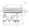
- FIG. 2 schematically illustrates an exemplary device structure of a pixel included in an imaging device of the present disclosure.
- the pixel 10Aa illustrated in FIG. 2 is an example of the above-described pixel 10A.
- FIG. 2 schematically shows the arrangement of the components constituting the pixel 10A, and the dimensions of the components shown in FIG. 2 do not necessarily reflect the dimensions of the actual device. The same applies to the other drawings of the present disclosure.
- the pixel 10Aa illustrated in FIG. 2 schematically includes a semiconductor substrate 80, an insulating layer 90 covering the semiconductor substrate 80, and a dielectric constant modulation element 20a supported by the insulating layer 90.
- Insulating layer 90 typically includes two or more insulating layers formed of silicon dioxide.
- the dielectric constant modulation element 20 a is an example of the above-described dielectric constant modulation element 20.
- an optical filter 86 such as a color filter, a microlens 88, and the like may be disposed above the dielectric constant modulation element 20a.
- the dielectric constant modulation element 20a faces the pixel electrode 22e supported by the insulating layer 90, the counter electrode 21e located farther from the semiconductor substrate 80 than the pixel electrode 22e, and the pixel electrode 22e. It includes a dielectric constant modulation structure 26a located between it and the electrode 21e.
- the counter electrode 21 e corresponds to the first terminal 21 of the dielectric constant modulation element 20 described above
- the pixel electrode 22 e corresponds to the second terminal 22.
- the pixel electrode 22e is electrically separated from the pixel electrode 22e of the adjacent other pixel 10Aa by being spatially separated from the adjacent other pixel 10Aa.
- a material of the pixel electrode 22e for example, a conductive material such as TiN or TaN which is stable and exhibits high light shielding property can be used.
- the counter electrode 21 e is formed of, for example, a translucent conductive material such as ITO.
- translucent in the present specification means that at least a part of the light in the wavelength range to be detected is transmitted, and it is essential to transmit the light over the entire wavelength range of visible light. Absent.
- the light detected by the imaging device of the present disclosure is not limited to light in the wavelength range of visible light, that is, light having a wavelength of 380 nm or more and 780 nm or less. In the present specification, all electromagnetic waves including infrared rays and ultraviolet rays are referred to as “light” for convenience.
- the counter electrode 21e is typically formed in the form of a single continuous electrode across the plurality of pixels 10Aa. Therefore, by connecting the power supply line 70 to the counter electrode 21 e, a desired voltage can be applied collectively to the counter electrodes 21 e of the plurality of pixels 10 Aa via the power supply line 70. Of course, it is not essential that the counter electrode 21e is continuous between all the pixels 10Aa. For example, the counter electrodes 21e may be separated for each row or column among the plurality of pixels 10Aa. .
- the light passing through the counter electrode 21e is incident on the dielectric constant modulation structure 26a.
- the dielectric constant modulation structure 26a is irradiated with light to change its dielectric constant. Detecting light through a change in dielectric constant in dielectric constant modulation structure 26 a by causing light to enter dielectric constant modulation structure 26 a in a state where a predetermined potential difference is given between pixel electrode 22 e and counter electrode 21 e Can. Details of the configuration of the dielectric constant modulation structure 26 a and details of the mechanism of light detection using the change of the dielectric constant in the dielectric constant modulation structure 26 a will be described later.
- the pixel electrode 22 e is electrically connected to the impurity region 30 a formed in the semiconductor substrate 80 through the connection portion 95 a disposed inside the insulating layer 90.
- a P-type silicon substrate is illustrated as the semiconductor substrate 80.
- the impurity region 30a is, for example, an N-type diffusion region.
- the junction capacitance formed by the pn junction including the impurity region 30 a can function as the above-described capacitance element 30.
- the semiconductor substrate 80 is not limited to a substrate that is entirely a semiconductor, and may be an insulating substrate or the like in which a semiconductor layer is provided on the surface on the side where the dielectric constant modulation element 20a is disposed.
- a signal detection transistor 41 and an address transistor 42 can be further formed.
- the plug 91 is connected to the gate electrode 41 g of the signal detection transistor 41.
- the plug 91 is connected to the plug 93 a connected to the above-described impurity region 30 a via the wiring 92. That is, the connection portion 95 a also has a connection with the gate electrode 41 g of the signal detection transistor 41.
- the plug 91 and the plug 93a are typically polysilicon plugs.
- the wire 92 is, for example, a polysilicon wire
- the plug 94 for connecting the wire 92 and the pixel electrode 22e to each other is, for example, a metal plug formed of copper or the like.
- Semiconductor substrate 80 further includes impurity regions 81, 82 and 83 and element isolation region 84.
- the impurity region 81 has a function as a drain region of the signal detection transistor 41
- the impurity region 82 has a function as a source region of the signal detection transistor 41.
- the address transistor 42 shares the impurity region 82 with the signal detection transistor 41, and the impurity region 82 also functions as a drain region of the address transistor 42.
- Impurity region 83 functions as a source region of address transistor 42.
- the above-mentioned output signal line 74 is connected to the impurity region 83.
- the output signal line 74 is not shown in FIG.
- An address signal line connected to the row scanning circuit is connected to the gate electrode 42 g of the address transistor 42.
- a wiring layer 96 is disposed in the insulating layer 90.
- the wiring layer 96 includes the output signal line 74 described above, an address signal line, and the like in part thereof.
- the dielectric constant modulation element 20a includes the dielectric constant modulation structure 26a sandwiched between the pixel electrode 22e and the counter electrode 21e.
- the dielectric constant modulation structure 26a has a laminated structure including the first charge blocking layer 23, the second charge blocking layer 24, and the photoelectric conversion layer 25 located between these blocking layers. .
- the photoelectric conversion layer 25 is irradiated with light to generate excitons inside.
- a typical example of the material of the photoelectric conversion layer 25 is a semiconductor material.
- an organic-semiconductor material is illustrated as a material which comprises the photoelectric converting layer 25.
- FIG. For example, a compound semiconductor material typified by hydrogenated amorphous silicon, CdSe or the like, or a metal oxide semiconductor material such as ZnO can be used as the material of the photoelectric conversion layer 25.
- the photoelectric conversion layer 25 may include a laminated structure of a donor organic compound and an acceptor organic compound, in other words, a heterojunction. Alternatively, a mixed layer having a bulk heterojunction structure may be included. The photoelectric conversion layer 25 may be a combination of these. The light incident on the photoelectric conversion layer 25 can be absorbed by either the donor organic compound or the acceptor organic compound or both of them.
- the first charge blocking layer 23 is located between the counter electrode 21 e and the photoelectric conversion layer 25, and suppresses exchange of charge between the counter electrode 21 e and the photoelectric conversion layer 25. That is, the first charge blocking layer 23 has a function of suppressing the movement of charges from the photoelectric conversion layer 25 to the counter electrode 21 e and the movement of charges from the counter electrode 21 e to the photoelectric conversion layer 25.
- the second charge blocking layer 24 is located between the pixel electrode 22e and the photoelectric conversion layer 25, and moves charge from the photoelectric conversion layer 25 to the pixel electrode 22e, and photoelectric conversion from the pixel electrode 22e. The transfer of charge to layer 25 is suppressed.
- the voltage supply circuit 50 applies a predetermined voltage to, for example, the counter electrode 21e, whereby a potential difference is given between the counter electrode 21e and the pixel electrode 22e. Therefore, the dielectric constant modulation structure 26a is in a state where an electric field is applied from the outside. Therefore, if, for example, the first charge blocking layer 23 is not provided in the dielectric constant modulation structure 26a, the counter electrode from the photoelectric conversion layer 25 when the counter electrode 21e has a high potential with respect to the pixel electrode 22e. The negative charge moves to 21 e, and the positive charge can move to the photoelectric conversion layer 25 from the counter electrode 21 e.
- the movement of charges between the photoelectric conversion layer 25 and the counter electrode 21 e is suppressed, and the photoelectric conversion layer is formed.
- the charge in 25 can be retained in the photoelectric conversion layer 25.
- the counter electrode 21e is set to a high potential with respect to the pixel electrode 22e
- by disposing the electron blocking layer as the first charge blocking layer 23 movement of electrons from the photoelectric conversion layer 25 to the counter electrode 21e can be performed. It can be restricted.
- a hole blocking layer as the second charge blocking layer 24 the movement of holes from the photoelectric conversion layer 25 to the pixel electrode 22e can be restricted.
- the photoelectric conversion layer 25 generates excitons in the photoelectric conversion layer 25 by the incidence of light through the counter electrode 21 e.
- excitons When excitons are generated in a state in which the movement of charge between the photoelectric conversion layer 25 and the electrode is suppressed, the charge density in the counter electrode 21 e and the pixel electrode 22 e is increased.
- the generation of excitons in a state where a potential difference is given between the counter electrode 21e and the pixel electrode 22e contributes to the change in polarization in the dielectric constant modulation structure 26a. Therefore, the increase in charge density at the electrodes results in an increase in the dielectric constant between the counter electrode 21e and the pixel electrode 22e, in other words, an increase in the dielectric constant of the dielectric constant modulation structure 26a.
- the capacitance value between the counter electrode 21 e and the pixel electrode 22 e is changed by the light irradiation.
- Light can be detected by detecting a change in the dielectric constant of the dielectric modulation structure 26a by means of the detection circuit 40, for example, in the form of a change in voltage.
- the photoelectric conversion layer 25 may be mainly made of an organic semiconductor material. That is, the dielectric constant modulation structure 26a may be a structure consisting essentially of an organic material.
- the materials of the first charge blocking layer 23 and the second charge blocking layer 24 are not limited to insulating materials. As described below, by appropriately selecting the material of the adjacent layer or electrode, the material which exhibits the property of transporting the charge of one polarity but not the charge of the opposite polarity by the application of voltage is selected as the first It can be used as a material of the charge blocking layer 23 and the second charge blocking layer 24.
- a hole transportable organic compound can be used as a material of the first charge blocking layer 23.
- a conductive material having a Fermi level shallower than the energy level of the highest occupied molecular orbital of the first charge blocking layer 23 as a material of the counter electrode 21 e
- a Schottky barrier between the electrode and the electrode It is possible to suppress both the movement of holes from the counter electrode 21 e to the first charge blocking layer 23 and the movement of electrons from the first charge blocking layer 23 to the counter electrode 21 e by using Similarly, when the counter electrode 21e is set to a high potential with respect to the pixel electrode 22e, an electron transporting organic compound can be used as a material of the second charge blocking layer 24.
- the second charge blocking layer from the pixel electrode 22 e Both the movement of electrons to 24 and the movement of holes from the second charge blocking layer 24 to the pixel electrode 22e can be suppressed.
- the energy level of the highest occupied molecular orbital may be simply referred to as the “HOMO level”
- the energy level of the lowest unoccupied molecular orbital may be simply referred to as the “LUMO level”.
- the photoelectric conversion layer 25 has a LUMO level of 4.0 eV and the pixel electrode 22 e is formed of an electrode material having a Fermi level of 5.1 eV.
- the above-described TiN is an electrode material having a Fermi level of about 5.1 to 5.2 eV, and can be applied to the material of the pixel electrode 22e.
- a hole blocking layer formed of an electron transporting organic compound can be used for the second charge blocking layer 24.
- the energy in the hole transport process between the photoelectric conversion layer 25 and the second charge blocking layer 24 As the barrier becomes larger, the ability to inhibit the movement of holes is improved.
- the fullerene has a LUMO level of 4.0 eV and a HOMO level of 6.4 eV. Therefore, it can be applied to the material of the second charge blocking layer 24 in this case.
- the energy barrier in the electron transport process is lowered as the LUMO level of the second charge blocking layer 24 is equal to or deeper than 4.0 eV, and the electron transport efficiency from the photoelectric conversion layer 25 toward the pixel electrode 22 e Improve.
- the counter electrode 21e has a high potential with respect to the pixel electrode 22e, and such movement of electrons may not be considered.
- the materials constituting the first charge blocking layer 23 and the second charge blocking layer 24 may be made of known materials in consideration of bond strength, stability, difference in ionization potential, difference in electron affinity, etc. between adjacent layers. It can be selected.
- the effect of retaining charges in the photoelectric conversion layer 25 can be obtained by providing the dielectric constant modulation structure 26 a with at least one of the first charge blocking layer 23 and the second charge blocking layer 24.
- the 1st charge blocking layer 23, the 2nd charge blocking layer 24, and the photoelectric converting layer 25 were organic materials was described, when these layers are inorganic compounds, it is HOMO. Is the valence band, and LUMO may be replaced with the conduction band.
- the HOMO level of the organic material can be determined, for example, by photoelectron spectroscopy, photoelectron yield spectroscopy, or the like.
- the LUMO level can be determined by inverse photoelectron spectroscopy or by subtracting the energy at the end of the absorption spectrum from the HOMO level.
- an insulating layer may be disposed instead of one or both of the first charge blocking layer 23 and the second charge blocking layer 24.
- the insulating layer may be disposed anywhere between the counter electrode 21 e and the photoelectric conversion layer 25 and between the pixel electrode 22 e and the photoelectric conversion layer 25.
- the insulating layer may be disposed both between the counter electrode 21 e and the photoelectric conversion layer 25 and between the pixel electrode 22 e and the photoelectric conversion layer 25.
- oxides such as SiO 2 , Al 2 O 3 , HfO 2 , and ZrO 2 , nitrides such as SiN, or compounds obtained by combination thereof, or polymethyl methacrylate resin (PMMA)
- PMMA polymethyl methacrylate resin
- FIG. 3 is an equivalent circuit diagram of the dielectric constant modulation element 20 a in the pixel 10 Aa and the impurity region 30 a as the capacitive element 30.
- the dielectric constant modulation structure 26a in the dielectric constant modulation element 20a changes its dielectric constant according to the amount of incident light. Further, since the dielectric constant modulation structure 26a includes the charge blocking layer or the insulating layer, basically no direct current flows between the dielectric constant modulation structure 26a and the pixel electrode 22e. From these things, in FIG. 3, the dielectric constant modulation element 20a is conveniently expressed using the circuit symbol similar to a variable capacitance.
- the voltage applied from the voltage supply circuit 50 to the first terminal 21 side of the dielectric constant modulation element 20a, that is, the counter electrode 21e is denoted as V IN .
- the voltage of the node M between the second terminal 22 side of the dielectric constant modulation element 20a, in other words, between the dielectric constant modulation element 20a and the capacitive element 30 (for example, the impurity region 30a) is denoted as V OUT .
- the detection circuit 40 described above is connected to the node M. Therefore, the above-described detection circuit 40 outputs a signal corresponding to the voltage V OUT .
- the set of the signal detection transistor 41 and the address transistor 42 shown in FIG. 1 is only an example of the detection circuit 40, and the configuration of the detection circuit 40 is as shown in FIG. 1 if it has the same function. It is not limited to.
- the charge density in the counter electrode 21e and the pixel electrode 22e increases due to the generation of excitons, and the capacitance value between the counter electrode 21e and the pixel electrode 22e changes. That is, the capacitance value C PC changes due to the light irradiation.
- the capacitance value C ref of the capacitance element 30 hardly changes due to the light irradiation to the pixel 10Aa, and the change of the capacitance value C ref due to the light irradiation is sufficiently compared with the change of the capacitance value C PC It is assumed that it is small. In this case, the voltage V OUT of the node M changes in accordance with the change of the capacitance value C PC of the dielectric constant modulation structure 26 a.
- FIG. 4 shows a change in V OUT with respect to a change in capacitance value C PC when a voltage of 5 V is applied as V IN and C ref is 1.2 fF.
- C PC capacitance value
- V OUT which is the potential of the second terminal 22 is also increased. Therefore, by connecting the detection circuit 40 to the node M, it is possible to detect a change in illuminance for the pixel 10Aa in the form of a change in input voltage to the signal detection transistor 41 as a source follower.
- the initial value of the capacitance value C PC for example, the capacitance value C PC of the dielectric constant modulation structure 26 a in a state where light is not irradiated is larger than the capacitance value C ref . If so, the change in the voltage V OUT with respect to the increase of the capacitance value C PC due to the light irradiation becomes small. Therefore, it is beneficial to have a relatively large capacitance value to the capacitive element 30 is capacitance C PC initial value.
- light can be detected through the change of the dielectric constant of the dielectric constant modulation element 20 due to the irradiation of light. Furthermore, in the embodiment of the present disclosure, unlike the configuration in which holes or electrons generated by photoelectric conversion are taken out as signal charges and the charge amount is read out, charges are not taken out from the dielectric constant modulation element 20. Therefore, by controlling the voltage applied from the voltage supply circuit 50 to the dielectric constant modulation element 20, for example, the potential difference between the counter electrode 21e and the pixel electrode 22e approaches 0V.
- the reset operation by the supply of the reset voltage can be basically eliminated.
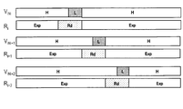
- FIG. 5 is a timing chart to explain an exemplary operation of an imaging device according to an embodiment of the present disclosure.
- the uppermost graph shows the change of the voltage V IN supplied from the voltage supply circuit 50 to the power supply line 70
- the middle graph shows the potential V of the address signal line connected to the gate of the address transistor 42. Indicates a change in SEL .
- the lowermost graph shows changes in the voltage VAD for controlling the drive of the AD conversion circuit 62.
- the voltage supply circuit 50 has a configuration capable of switching at least two different voltages.
- the voltage supply circuit 50 can selectively supply either the high level first voltage or the low level second voltage lower than the first voltage to the power supply line 70.
- the voltage V OUT applied to the gate of the signal detection transistor 41 of the detection circuit 40 is the voltage V IN applied to the first terminal 21 of the permittivity modulation element 20, in other words
- the voltage supply circuit 50 is proportional to the voltage applied to the power supply line 70.
- the capacitance value C PC of the dielectric constant modulation structure 26a changes according to the illuminance, and the voltage V OUT also changes accordingly, but if the voltage V IN is small, the voltage V OUT accompanying the change of the illuminance Change is also small.
- the potential of the electrode of the capacitive element 30 not connected to the node M is the ground. Therefore, assuming that the low level second voltage is, for example, ground, ie, 0 V, the voltage V OUT applied to the gate of the signal detection transistor 41 is basically 0 V regardless of the illuminance. Therefore, it can be said that the period in which the voltage supply circuit 50 applies the low level second voltage to the power supply line 70 corresponds to the non-exposure period.
- the second voltage is applied to the power supply line 70 in the initial state.
- the second voltage is 0V.
- the voltage supply circuit 50 sets the voltage applied to the power supply line 70 to the high level first voltage.
- the voltage V IN applied to the counter electrode 21 e of the dielectric constant modulation element 20 a is made the first voltage
- the voltage V OUT has a capacitance value C corresponding to the illuminance, as can be seen from the equation (1) and FIG. It changes with the change of PC . That is, the voltage V OUT corresponding to the illuminance is applied to the gate of the signal detection transistor 41.
- the potential V SEL of the address signal line is set to the high level, and the address transistor 42 is turned on.
- a signal corresponding to the illuminance is output from the detection circuit 40 of the selected pixel 10A to the output signal line 74.
- a voltage signal corresponding to the illuminance is output to the output signal line 74.
- the drive pulse of the AD conversion circuit 62 is raised at time t3. That is, the AD conversion circuit 62 is operated in a state where the voltage supply circuit 50 supplies the high-level first voltage to the power supply line 70 and the address transistor 42 is turned on.
- the digital value obtained at this time by the operation of the AD conversion circuit 62 is the pixel signal corresponding to the illuminance in this example.
- the voltage supply circuit 50 switches the voltage supplied to the power supply line 70 to the low level second voltage.
- the voltage supplied to the power supply line 70 By switching the voltage supplied to the power supply line 70 to the second voltage, the potential difference between the counter electrode 21 e and the pixel electrode 22 e is reduced, and positive and negative generated in the photoelectric conversion layer 25 by light irradiation.
- the pair of charges quickly recombine.
- the voltage V OUT since the second voltage is 0V, the voltage V OUT is 0V. That is, the voltage V OUT applied to the gate of the signal detection transistor 41 returns to the state before the high level first voltage is supplied to the power supply line 70. That is, in the embodiment of the present disclosure, a period in which the voltage supply circuit 50 supplies a relatively high voltage to each pixel 10A can be regarded as an exposure period.
- the double arrow EXP in FIG. 5 schematically represents this exposure period.
- the drive pulse of the AD conversion circuit 62 is raised again.
- a digital value corresponding to the signal of the reference level before the high level first voltage is supplied to the power supply line 70 is obtained.
- the signal processing circuit 60 generates and outputs the difference between the digital value obtained at time t3 and the digital value obtained at time t5. That is, the signal processing circuit 60 generates a pixel signal obtained during a period in which the first voltage of high level is supplied to the power supply line 70 as a signal indicating the illuminance of the object, and a second voltage of low level to the power supply line 70. Generates a difference with the signal of the reference level obtained during the period in which Thereafter, at time t6, the address transistor 42 is turned off.
- the signal component thus obtained is compared with the case where the signal component obtained when a high level voltage is applied to the first terminal 21 is directly output as a signal indicating the illuminance of the object, The noise component is suppressed.
- the order of the detection of the pixel signal and the detection of the signal of the reference level is not limited to the example shown in FIG. 5, and the detection of the signal of the reference level may be performed first.
- the difference between the outputs of the detection circuit 40 is not limited to the form of the difference between the digital values, and may be, for example, the form of the difference between the amplitudes of the analog waveforms.
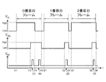
- FIG. 6 shows an example of an imaging operation over a plurality of frames.
- the voltage applied from the voltage supply circuit 50 to the power supply line 70 is set to the high level first voltage at time t11.
- the start of the application of the first voltage by the voltage supply circuit 50 corresponds to the start of the exposure period of the 0th frame period.
- the address transistor 42 is turned on at time t12. Further, by operating the AD conversion circuit 62 at time t13, a pixel signal according to the illuminance can be obtained.
- the voltage applied from the voltage supply circuit 50 to the power supply line 70 is switched to the low level second voltage.
- the timing of switching to the second voltage corresponds to the end of the exposure period in the zeroth frame period.
- the AD conversion circuit 62 is operated again at time t15, and a signal of the reference level is acquired. Thereafter, at time t16, the address transistor 42 is turned off, and the 0th frame period ends.
- the signal processing circuit 60 generates a difference between the pixel signal and the signal of the reference level obtained at time t15 as a signal indicating the illuminance of the subject.
- the voltage applied by the voltage supply circuit 50 to the power supply line 70 is again switched to the high level first voltage, whereby the next frame period, that is, the first frame period is started.
- the address transistor 42 is turned on at time t22, and the AD conversion circuit 62 is operated at time t23 to acquire a pixel signal corresponding to the illuminance for the first frame. .
- the voltage applied to the power supply line 70 is switched to the low level second voltage, and the address transistor 42 is turned off. Furthermore, the voltage applied to the power supply line 70 is switched to the first voltage again at time t31 without acquiring the signal of the reference level. In other words, the second frame period has begun.
- the signal processing circuit 60 generates a difference between the pixel signal obtained at time t23 and the signal of the reference level obtained at time t15 in the 0th frame period as a signal indicating the illuminance of the subject.
- the voltage V IN applied to the first terminal 21 is returned to the initial state, in other words, the voltage applied by the voltage supply circuit 50 to the power supply line 70 is low.
- the state of the dielectric constant modulation element 20 can be returned to the state before the light irradiation. That is, the potential of the node M can be substantially reset without executing the reset operation by supplying the reset voltage to the pixel.
- the operation in the subsequent second frame period may be similar to the operation in the first frame period.
- the address transistor 42 is turned on at time t32, and the AD conversion circuit 62 is operated at time t33 to obtain a pixel signal corresponding to the illuminance for the second frame.
- the voltage V IN is switched to the second voltage at time t34 and the address transistor 42 is turned off, whereby the second frame period ends.
- the point that the signal processing circuit 60 generates a difference between the pixel signal obtained at time t33 and the signal of the reference level obtained in the 0th frame period as a signal indicating the illuminance of the object is the first point. It is similar to the frame.
- the number of times the voltage supply circuit 50 reads the signal through the detection circuit 40 during the period in which the voltage supply circuit 50 supplies the second voltage to each pixel 10A. It may be less than the number of times the signal is read out through the detection circuit 40 during the period of supplying the first voltage. That is, the number of times of reading of the signal of the reference level may be smaller than the number of times of reading of the pixel signal according to the illuminance. According to such an operation, since acquisition of the signal of the reference level for each frame period is omitted, the period required for signal readout can be shortened and imaging can be performed at high speed. Alternatively, the exposure time can be lengthened by omitting the acquisition of the signal of the reference level for each frame period, and a higher SN ratio can be realized.
- FIG. 7 schematically illustrates an example of the read operation of the imaging device including a plurality of pixels arranged in two dimensions.
- the white rectangle H in the top row represents the first period during which the voltage supply circuit 50 applies the first voltage of high level to the first terminal 21, and the hatched rectangle L represents the voltage supply circuit. 50 represents a second period in which a low level second voltage is applied to the first terminal 21.
- a common voltage is applied to the counter electrode 21e of each pixel 10Aa.
- FIG. 7 representatively shows operations of a pixel belonging to the i-th row, a pixel belonging to the (i + 1) -th row, and a pixel belonging to the (i + 2) -th row among a plurality of rows.
- white rectangles Exp represent exposure periods in each row
- shaded rectangles Rd represent signal readout periods.
- the readout of the pixel signal and the readout of the signal of the reference level are executed at the timing represented by the rectangle Rd.
- the readout of the pixel signal is performed in the first period, and the readout of the signal of the reference level is performed in the second period.
- acquisition of a signal of a reference level for each frame period may be omitted.
- readout of the pixel signal and the signal of the reference level is sequentially performed while shifting the timing on a row basis.
- FIG. 8 schematically shows another example of the readout operation of the imaging device including a plurality of pixels arranged in a two-dimensional manner.
- the shaded rectangle Rd1 represents the readout period of the pixel signal
- the shaded rectangle Rd2 represents the readout period of the signal of the reference level.
- readout of pixel signals is sequentially performed in row units in a first period
- readout of signals of a reference level is sequentially performed in row units in a second period.
- voltage switching from the first voltage to the second voltage and switching from the second voltage to the first voltage may be performed once in one frame period.
- FIG. 9 and FIG. 10 schematically show still another example of the readout operation of the imaging device including a plurality of pixels arranged in two dimensions.
- signal readout is performed at common timing for all the rows, and the start and end of the exposure period are common to all the pixels. That is, a so-called global shutter is realized.
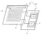
- the signal processing circuit 60 and an XY decoder for designating a specific pixel in the imaging area are arranged on a chip different from the chip in which the imaging area is formed. For example, these chips are stacked. This can be realized by electrically connecting each row of a plurality of pixels to the signal processing circuit 60. An analog-digital conversion circuit may be arranged in each pixel. According to the chip stacking technology, it is possible to realize an imaging device adapted to such a reading method while avoiding an increase in size of a pixel.
- FIG. 10 shows an operation example applicable to a pixel having a frame memory.
- a shaded rectangle Trs represents a period for transferring information on the signal level to the frame memory.
- FIG. 10 shows an example in which the voltage level of the pixel signal obtained in the exposure period is transferred to the frame memory, and the voltage level of the pixel signal is read out from the frame memory during the exposure period of the next frame period. Note that the reading of the signal of the reference level may be performed in the second period in any frame period.
- FIG. 11 shows an example of a pixel having a frame memory.
- the pixel 10B shown in FIG. 11 includes a set of a transfer transistor 45 connected between the node M and the gate of the signal detection transistor 41, and a capacitive element 44 having one electrode connected to the gate of the signal detection transistor 41. .
- the other electrode of the capacitor 44 for example by being connected to a power supply (not shown), capable of applying configured the predetermined voltage V G during operation of the imaging apparatus 100A.
- the voltage level of the node M after exposure can be temporarily held by the capacitive element 44 by turning on the transfer transistor 45 after the lapse of a predetermined period from the start of the first period and turning it off again. After the voltage level is held in the capacitive element 44, a signal corresponding to the voltage level held in the capacitive element 44 can be read out to the output signal line 74 at a desired timing by turning on the address transistor 42. .
- the transfer transistor 45 and off can be controlled, for example, by a row scanning circuit (not shown). From the viewpoint of increasing sensitivity, it is useful that the capacitive element 44 have a capacitance value smaller than that of the capacitive element 30 (for example, the impurity region 30a).
- the potential of the node M is substantially 0 V regardless of light irradiation. Therefore, the reset operation required for a general imaging device is basically unnecessary.
- the voltage applied to the electrode on the side not connected to the node M among the electrodes of the capacitive element 30 and the second voltage applied to the dielectric constant modulation element 20 by the voltage supply circuit 50 do not match. I assume. In such a case, when the voltage applied to the dielectric constant modulation element 20 is switched to the first voltage, the potential of the node M can rise from 0 V even without light irradiation.
- the signal processing circuit 60 may obtain the pixel signal obtained during the period in which the first voltage of high level is supplied to the power supply line 70 and the period during which the second voltage of low level is supplied to the power supply line 70.
- a signal obtained by further subtracting the signal corresponding to the offset level from the difference from the signal of the reference level may be output as a signal indicating the illuminance of the subject.
- the subtraction of the signal corresponding to the offset level may be performed in the form of subtraction of digital signals or may be performed in the form of subtraction of analog signals. By subtracting the signal corresponding to the offset level, it is possible to reduce fixed pattern noise due to the variation of the offset level for each pixel.
- the signal corresponding to the offset level is not irradiated with light to the dielectric constant modulation element 20, and the detection circuit 40 is in a state in which the high-level first voltage is supplied from the voltage supply circuit 50 to the power supply line 70. It is a signal to be output. As described below, the signal corresponding to the offset level can be obtained by various methods.
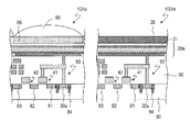
- FIG. 12 shows a first example of a configuration capable of acquiring a signal corresponding to the offset level.
- the imaging device has an array of a plurality of pixels including a dummy pixel 10Dm in addition to the above-described pixel 10Aa.
- the light shielding layer 28 covers the dielectric constant modulation element 20a and blocks the incidence of light on the dielectric constant modulation element 20a.
- the basic device structure of the dummy pixel 10Dm is similar to that of the pixel 10Aa except that it has the light shielding layer 28.
- the optical filter 86 and the micro lens 88 can be abbreviate
- Incident of light to the dielectric constant modulation element 20 a of the dummy pixel 10 Dm is prevented by the light shielding layer 28. Therefore, by reading out the output of the detection circuit 40 of the dummy pixel 10Dm in the state where the first voltage is applied to the counter electrode 21e, a signal corresponding to the offset level can be obtained with a relatively simple configuration.
- Such dummy pixels 10Dm may be arranged in the peripheral area outside the imaging area formed from the array of the pixels 10Aa. Such a configuration is effective particularly when the influence of the variation in the offset level for each pixel is small.
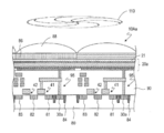
- FIG. 13 shows a second example of a configuration capable of acquiring a signal corresponding to the offset level.
- the imaging device has a mechanical shutter 110 that switches the incidence and blocking of light to each pixel 10Aa.
- a pixel signal can be obtained through the detection circuit 40.
- a signal corresponding to the offset level can be obtained by acquiring the output from the detection circuit 40 in a state in which the first voltage is applied to the counter electrode 21e and in a state in which the mechanical shutter 110 is closed.
- the mechanical shutter 110 that operates in synchronization with the signal processing circuit 60 may be used to obtain a signal corresponding to the offset level. According to the second example described here, even if the offset level is different for each pixel, it is possible to accurately obtain the offset.
- FIG. 14 shows a third example of the configuration capable of acquiring a signal corresponding to the offset level.
- An imaging device 100B illustrated in FIG. 14 includes a light source 120 and a control circuit 130 that synchronously drives the light source 120 and the plurality of pixels 10Aa.
- the light source 120 irradiates the object Ob with light of a predetermined wavelength range, for example, infrared light, in the first period in which the high level first voltage is applied to the counter electrode 21 e.
- the plurality of pixels 10Aa output a signal based on the reflected light of a predetermined wavelength range from the subject Ob.
- the signal detected by the detection circuit 40 of the pixel 10Aa in a state in which the light source 120 is turned off and the first voltage of high level is applied to the counter electrode 21e corresponds to the signal corresponding to the offset level.
- the configuration as illustrated in FIG. 14 is also useful.
- the configuration as illustrated in FIG. 14 is particularly useful when detecting light in a wavelength range in which the intensity included in ambient light is small.
- infrared light having a wavelength of about 900 nm or more for indoor photographing and about 1400 nm for outdoor photographing can be used as light emitted from the light source 120.
- the detection circuit of each pixel 10Aa in the state where the light source 120 is turned off and the first voltage of high level is applied to the counter electrode 21e.
- the signal detected by 40 gives the correct value of the signal corresponding to the offset level.
- All of the first to third examples are examples in which an output corresponding to the signal level in the dark is used as a signal corresponding to the offset level.
- the voltage supply circuit 50 switches the voltage applied to the power supply line 70 from the low level second voltage to the high level first voltage, in other words, detection is performed at the very beginning of the first period corresponding to the exposure period.
- the signal output from the circuit 40 may be acquired as a signal corresponding to the offset level.
- an offset level corresponding to each pixel can be obtained.
- the signal corresponding to the offset level for each pixel may be read once at a timing different from that for reading the pixel signal.
- the potential of the node M may be obtained in advance for each pixel under dark conditions, and a signal corresponding to the potential obtained at this time may be used as a signal corresponding to the offset level.
- a memory may be provided in the signal processing circuit 60, and the value of the offset level may be held in advance in the memory.
- a configuration may be adopted in which the value of the offset level in the memory is updated by performing calibration at an arbitrary timing. If the variation in the offset level for each pixel is small, the common offset level may be uniformly applied to all the pixels.
- FIG. 15 shows a modification in which a reset transistor is provided in a pixel.
- the pixel 10C illustrated in FIG. 15 includes a reset transistor 46 connected to the node M.
- one of the source and the drain of the reset transistor 46 is electrically connected to a terminal (for example, the pixel electrode 22e) connected to the node M of the permittivity modulation element 20a.
- the other of the source and the drain of the reset transistor 46 is supplied with a predetermined reset voltage VRef .
- the reset transistor 46 is turned on, the potential of the pixel electrode 22e, in other words, the potential of the node M, is reset to V Ref .
- the on and off of the reset transistor 46 is controlled, for example, by applying a reset signal V RST to the gate of the reset transistor 46 from a row scanning circuit (not shown).
- the charge generated by photoelectric conversion is not extracted to the node M and stored in the node M.
- the voltage V IN applied to the terminal (for example, the counter electrode 21 e) opposite to the node M of the dielectric constant modulation element 20 a to, for example, 0 V
- the voltage V OUT of the node M in other words, If so, the input to the detection circuit 40 can be 0V. Therefore, if the voltage supply circuit 50 switches the voltage applied to the power supply line 70 from the high level first voltage to the low level second voltage, exposure of the next frame is performed without applying the reset voltage to the node M. Can be started.
- the voltage applied to the first terminal 21 by the voltage supply circuit 50 is switched between the first voltage and the second voltage, Light can be detected by the detection circuit 40 detecting the potential of the node M in each of a first period in which the first voltage is supplied to the pixel and a second period in which the second voltage is supplied.
- a circuit for resetting the node M is basically unnecessary.
- the charge amount in the node M can be made uniform among a plurality of pixels.
- the potential of the node M before exposure can be adjusted to an arbitrary value among a plurality of pixels, and the variation in reference level for each pixel can be eliminated. Therefore, the advantage is obtained that the voltage range can be used effectively.
- the potential of the pixel electrode 22e after reset can be made equal to the potential of the counter electrode 21e.
- the reset voltage V Ref may be the same voltage as the second voltage.
- the voltage supply circuit 50 applies the second voltage to the counter electrode 21e in the second period, and the reset voltage V Ref is equal to the second voltage, the potential difference applied to the permittivity modulation structure 26a after the reset operation is approximately 0 V It is possible. Therefore, it is also possible to make the sensitivity of a specific pixel zero at any time.
- the reset voltage V Ref is supplied to the pixel electrode 22e by turning on the reset transistor 46 in the second period in which the second voltage is supplied to the pixel 10C. Reset of the potential of the pixel electrode 22e is performed.
- the readout of the signal of the reference level via the detection circuit 40 is performed after the reset of the potential of the pixel electrode 22 e by the reset transistor 46. As described above, readout of the signal of the reference level is performed, for example, once in the second period before the first frame period starts or in the second period in the first frame period among a plurality of consecutive frames. do it.
- the exposure period of the first frame period starts.
- the potential of the node M returns to V Ref .
- FIG. 16 shows another example of the device structure of a pixel.
- the difference between the pixel 10Ab shown in FIG. 16 and the pixel 10Aa shown in FIG. 2 is that the pixel 10Ab is disposed in the insulating layer 90 instead of the impurity region 30a as the capacitive element 30, MIM (metal a point having the capacitive element 30b of the (insulator-metal) structure.
- MIM metal a point having the capacitive element 30b of the (insulator-metal) structure.
- capacitive element 30 b includes upper electrode 33, lower electrode 34 located between upper electrode 33 and semiconductor substrate 80, and dielectric sandwiched between upper electrode 33 and lower electrode 34. It has a layer 35.
- the connection portion 95b in the pixel 10Ab includes a plug 93b that electrically connects the upper electrode 33 and the wiring 92 to each other.
- the lower electrode 34 is connected to a wire (not shown), its potential is fixed, for example, to ground during operation.
- the capacitive element 30 connected to the node M is not limited to the form of the junction capacitance formed by the pn junction, and may be realized in the form of an MIM structure like the capacitive element 30b. It may be realized in the form of a MOS capacitor in which the electrode is a semiconductor layer. When the MIM structure is applied, a part of the wiring layer 96 may be used as one or both of the upper electrode 33 and the lower electrode 34.
- the material of the dielectric layer 35 is, for example, an oxide such as SiO 2 , Al 2 O 3 , HfO 2 , ZrO 2 or a nitride such as SiN, or a compound obtained by a combination thereof, PMMA, polyimide And organic materials such as polystyrene can be widely used.
- a combination of different materials may form substantially one capacitive element.
- part of the insulating layer 90 may be used as the dielectric layer 35.
- the MIM structure of the capacitive element 30b is also referred to as a MOM structure.
- the capacitance element 30b has a structure in which the capacitance value hardly changes even when light is incident, or the change in capacitance value due to the light incidence is sufficiently smaller than the change in capacitance value in the dielectric constant modulation element 20a. It is formed as For example, as a material of the dielectric layer 35, a material such as SiO 2 whose dielectric constant hardly changes upon light incidence may be selected. Alternatively, TiN having high light shielding properties can be applied as a material of the upper electrode 33 and / or the lower electrode 34.
- the capacitive element 30 b may be disposed in the insulating layer 90 so that the periphery is covered with a light shielding material, and the incidence of light to the capacitive element 30 b may be suppressed.
- node M includes the interface between the silicon substrate and the contact plug. Absent. Therefore, it is possible to avoid the influence of dark current caused by interface states. If the reset transistor 46 is formed as a thin film transistor, generation of dark current due to the interface state can be avoided even in combination with the reset circuit including the reset transistor 46.
- the configuration of the dielectric constant modulation element 20 is also not limited to the configuration described with reference to FIG.
- a layer including quantum dots may be applied instead of the photoelectric conversion layer 25 in the dielectric constant modulation structure 26 a shown in FIG. 2. Quantum dots receive light incident to generate charge pairs. Also in this case, as in the example shown in FIG. 2, transfer of the insulating layer or charge to at least one of the layer including the quantum dot and the counter electrode 21 e and between the layer including the quantum dot and the pixel electrode 22 e A charge blocking layer is provided to suppress
- FIG. 17 shows another example of the dielectric constant modulation element 20.
- the pixel 10D shown in FIG. 17 includes a counter electrode 21e, a pixel electrode 22e, and a dielectric constant modulation element 20d including a dielectric constant modulation structure 26d located between the counter electrode 21e and the pixel electrode 22e.
- the dielectric constant modulation structure 26d is a layer including a material whose dielectric constant changes by light irradiation, such as hafnium oxide. With such a configuration as well, it is possible to detect light through the change of the dielectric constant of the dielectric constant modulation element 20d due to the light irradiation.
- the response of the dielectric constant in the dielectric constant modulation element 20 to the incidence of light may be nonlinear or linear with respect to the intensity or time of the incident light. In any case, light detection is possible.
- a dielectric constant modulation structure that exhibits a larger change in dielectric constant with respect to light irradiation as the potential difference between the counter electrode 21 e and the pixel electrode 22 e becomes larger. Since the amount of change of the dielectric constant between the time of detection of the signal is expanded, more sensitive detection can be performed.
- FIG. 18 schematically illustrates the configuration of an imaging device according to the second embodiment of the present disclosure.
- the imaging device 100E shown in FIG. 18 has a plurality of pixels 10E instead of the plurality of pixels 10A.
- the electrode not connected to the second terminal 22 of the dielectric constant modulation element 20 is a voltage supply circuit through the power supply lines 71 and 72. It is electrically connected to 50. That is, in this example, the voltage supply circuit 50 is configured to be capable of switching and supplying the first voltage and the second voltage to the second terminal 22 of the dielectric constant modulation element 20 via the capacitive element 30.
- the potential of the first terminal 21 is commonly fixed to, for example, the ground during operation.
- the voltage V OUT exhibits a decreasing change.
- the signal detection transistor 41 as a source follower is irradiated with light.
- the detection circuit 40 can detect the change in the dielectric constant of the dielectric constant modulation element 20 in the form of a voltage change.
- the voltage supply circuit 50 is configured to change the potential on the first terminal 21 side with reference to the potential on the second terminal 22 side of the dielectric constant modulation element 20 as in this example. It is also possible to change the potential of the electrode of the capacitive element 30 on the side not connected to the second terminal 22 based on the potential on the first terminal 21 side of the dielectric constant modulation element 20 as a reference. .
- the voltage supply circuit 50 may be configured such that a predetermined voltage can be applied to the other terminal with reference to either the first terminal 21 or the second terminal 22 of the dielectric constant modulation element 20.
- the voltage supply circuit 50 supplies a voltage to either the first terminal 21 side or the electrode on the side not connected to the second terminal 22 of the electrodes of the capacitive element 30, thereby the first terminal 21 and the second terminal 22.
- the potential difference between and can be uniquely determined.
- the potential difference applied to dielectric constant modulation structure 26a or 26d is also uniquely determined.
- the capacitive element 30 is interposed between the second terminal 22 of each pixel 10E and the voltage supply circuit 50, but the voltage supplied by the voltage supply circuit 50 causes the first terminal 21 and It can be said that the potential difference with the second terminal 22 is substantially controlled.
- the power supply line 71 is connected to the capacitive elements 30 of the two pixels 10E belonging to the first row, and the capacitive elements 30 of the two pixels 10E belonging to the second row are electrically Line 72 is connected. Therefore, according to such a form of connection, the potential of node M can be individually controlled on a row basis.
- FIG. 19 schematically shows an example of the read operation in the imaging device 100E shown in FIG.
- the relationship between the change in V IN and the exposure period and the readout period is also shown.
- a shaded rectangle Rd represents a period during which the readout of the pixel signal and the readout of the signal of the reference level are performed.
- the readout of the pixel signal is performed in the first period, and the readout of the signal of the reference level is performed in the second period, as in the example described with reference to FIG.
- switching between the first voltage and the second voltage can be performed at any timing, for example, for each row. It is possible to carry out. Therefore, as shown in FIG. 19, it is possible to apply the readout operation similar to a so-called rolling shutter by shifting the period of switching between the first voltage and the second voltage and readout of the signal for each row.
- the readout operation similar to a so-called rolling shutter by shifting the period of switching between the first voltage and the second voltage and readout of the signal for each row.
- the exposure period can be expanded to enable imaging with an improved SN ratio.
- Such switching of voltages in units of rows can also be realized by patterning the counter electrode 21 e so as to be separated by each row of a plurality of pixels in a configuration in which the power supply line 70 is connected to the counter electrode 21 e.
- the power supply lines 71 and 72 are provided independently for each row of the plurality of pixels 10E, and switching between the first voltage and the second voltage is performed independently for each row.
- the invention is not limited to the example, and power supply lines connected to the voltage supply circuit 50 may be connected to each column of the plurality of pixels 10E or to each of the pixels 10E independently. That is, the voltage supply circuit 50 may be configured to be able to independently supply different voltages in units of columns or in units of pixels, and the potential of the node M may be individually controlled in units of columns or in units of pixels.
- FIG. 20 schematically illustrates an exemplary configuration of an imaging device according to a third embodiment of the present disclosure.
- An imaging device 100F illustrated in FIG. 20 includes an imaging element 200 and a signal processing circuit 60F that performs signal processing on an electrical signal from the imaging element 200.
- the image pickup device 200 includes, for example, a plurality of pixels 10A as in the above-described image pickup apparatus 100A, converts incident light into an electric signal, and outputs the electric signal to the signal processing circuit 60F.
- the imaging device 200 further includes a voltage supply circuit 50 that supplies a predetermined voltage to each of the pixels 10A.
- the point that the second voltage is supplied in different second periods is the same as each of the above-described examples.
- the signal processing circuit 60F is a pixel signal obtained during a period in which the high-level first voltage is supplied to the power supply line connected to the voltage supply circuit 50; A difference from the signal of the reference level obtained during the period in which the low level second voltage is supplied to the power supply line is generated and output.
- the signal processing circuit 60F is typically provided with AD conversion circuits 62 in the same number as the number of columns of the plurality of pixels 10A. In FIG. 20, two of these AD conversion circuits 62 are representatively shown for simplicity.
- the signal processing circuit 60F is a circuit substrate different from the semiconductor substrate 80. It is provided at 89.
- some circuits including the AD conversion circuit 62 may be formed on a substrate different from the substrate on which the pixels are arranged. For example, one camera system can be constructed by stacking these two substrates and electrically connecting them.
- the voltage supply circuit 50 sets the first voltage and the second voltage at one of the first terminal 21 and the second terminal 22 of the dielectric constant modulation element 20 as a reference.
- the voltage supply circuit 50 supplies the first voltage of high level to each pixel in the exposure period, and supplies the second voltage of low level to each pixel in the period of readout of the reference level.
- the detection circuit 40 reads the pixel signal at the level corresponding to the illuminance during the first period in which the voltage supply circuit 50 supplies the first voltage, and the voltage supply circuit 50 supplies the second voltage. During a period, readout of the signal of the reference level is performed.
- the first voltage and / or the second voltage may be applied as a pulse, or the application may be repeated periodically or quasi-periodically.
- Example 1 A sample imitating the above-described dielectric constant modulation element 20 was manufactured, the bias was changed, and the capacitance value was measured to evaluate the change in the dielectric constant with respect to the illuminance in the manufactured sample.
- FIG. 21 schematically shows the structure of a sample produced as Example 1. The samples were prepared as follows.
- a glass substrate 90S was prepared.
- the lower electrode 22S and the insulating layer 24S were formed on the glass substrate by sequentially depositing ITO and Al 2 O 3 on the glass substrate by sputtering and atomic layer deposition (ALD), respectively.
- ALD atomic layer deposition
- a tin naphthalocyanine (SnNc) and a fullerene (C 60 ) were sequentially deposited by vapor deposition to form a photoelectric conversion layer 25S.
- the thickness of each of the tin naphthalocyanine layer and the fullerene layer was approximately 75 nm.
- Example 1 After formation of the photoelectric conversion layer 25S, Al 2 O 3 and ITO were further deposited successively on the photoelectric conversion layer 25S by ALD and sputtering to form a laminated structure of the insulating layer 23S and the top electrode 21S.
- the sample of Example 1 was obtained by the above procedure.
- the thickness of the insulating layers 24S and 23S was about 20 nm
- the thickness of the photoelectric conversion layer 25S was about 150 nm
- the thickness of the top electrode 21S was about 50 nm.
- the bias V bias applied between the lower surface electrode 22S and the upper surface electrode 21S is changed to measure the current response to the AC voltage.
- the capacitance value between the and the top electrode 21S was measured.
- a capacitance value was measured in the sequential mode using an AC voltage amplitude of 100 mV and a measurement frequency of 100 Hz using a precision LCR meter 4284A manufactured by HEWLETT PACKARD.
- FIG. 22 shows, for each bias, the measurement results of the change in capacitance value when the illuminance is changed, with respect to the sample of Example 1.
- the horizontal axis of the graph shown in FIG. 22 indicates the intensity of light irradiated to the sample, and the vertical axis indicates the capacitance value between the lower surface electrode 22S and the upper surface electrode 21S.
- the unit of light intensity shown in FIG. 22 is an arbitrary unit.
- the imaging device of the present disclosure is applicable to an image sensor and the like. In particular, it is useful for an image sensor for detecting light in the infrared region susceptible to dark current.
- the imaging device of the present disclosure can be used for digital cameras, medical cameras, camera for machine vision (for example, cameras for robots), and the like.
- the machine vision camera can be used, for example, as an input for performing image recognition to determine the state of a product at a production plant, classification, or detection of a defect.
- Embodiments of the present disclosure are also useful for security cameras, cameras mounted on vehicles and the like.
- the on-vehicle camera may be used, for example, as an input to a control device for the vehicle to travel safely. Alternatively, it can be used to assist the operator for the vehicle to travel safely.
- An infrared image can be used, for example, for sensing such as distance detection and object recognition.
Abstract
This imaging device is provided with pixels each including: a permittivity modulation element including a first terminal, a second terminal, and a permittivity modulation structure located between the first terminal and the second terminal and having a permittivity that changes by light irradiation; a capacitive element including a first electrode and a second electrode, the second electrode being electrically connected to the second terminal of the permittivity modulation element; and a detection circuit which outputs a signal corresponding to the potential of the second terminal. The imaging device is further provided with a voltage supply circuit which applies first voltage to one of the first terminal of the permittivity modulation element and the first electrode of the capacitive element during a first period, and applies second voltage thereto during a second period different from the first period, and a signal processing circuit which generates a third signal that is a difference between a first signal outputted from the detection circuit during the first period and a second signal outputted from the detection circuit during the second period, and a potential difference between the first terminal and the first electrode when the second voltage is applied to the one is lower than a potential difference between the first terminal and the first electrode when the first voltage is applied to the one.
Description
本開示は、撮像装置に関する。
The present disclosure relates to an imaging device.
従来、光検出装置、イメージセンサなどに光検出素子が用いられている。光検出素子の典型例は、フォトダイオード、フォトトランジスタなどの光電変換素子である。よく知られているように、光の照射によって光電変換素子に生じる光電流を検出することにより、光を検出することができる。
Conventionally, a light detection element is used for a light detection device, an image sensor, and the like. Typical examples of the light detection element are photoelectric conversion elements such as a photodiode and a phototransistor. As well known, light can be detected by detecting a photocurrent generated in a photoelectric conversion element by light irradiation.
下記の特許文献1は、図2に、所定の化合物が有機重合体中に分散された有機膜をゲート絶縁膜として有する薄膜トランジスタ(TFT)を開示している。有機膜を構成する所定の化合物としては、光の照射によって分極の状態が変化する化合物が選ばれる。特許文献1の薄膜トランジスタでは、ゲート絶縁膜に光が照射されると、ゲート絶縁膜の誘電率が変化する。そのため、ゲート絶縁膜への光の照射によって、ソース-ドレイン間を流れる電流が変化する。特許文献1には、このような薄膜トランジスタを光センサに用いることが可能であると記載されている。
Patent Document 1 below discloses, in FIG. 2, a thin film transistor (TFT) having an organic film in which a predetermined compound is dispersed in an organic polymer as a gate insulating film. As the predetermined compound constituting the organic film, a compound whose polarization state is changed by light irradiation is selected. In the thin film transistor of Patent Document 1, when light is irradiated to the gate insulating film, the dielectric constant of the gate insulating film changes. Therefore, the light flowing to the gate insulating film changes the current flowing between the source and the drain. Patent Document 1 describes that such a thin film transistor can be used for an optical sensor.
下記の特許文献2および特許文献3は、光の照射によって生じる、光電変換層を挟む2つの電極の間の容量の変化または光電変換層の誘電率の変化を通して光を検出することが可能な装置を開示している。参考のために、国際公開第2017/081847号の開示内容の全ておよび国際公開第2017/081831号の開示内容の全てを本明細書に援用する。
Patent documents 2 and 3 listed below are devices capable of detecting light through change in capacitance between two electrodes sandwiching the photoelectric conversion layer or change in dielectric constant of the photoelectric conversion layer caused by light irradiation. Is disclosed. The entire disclosure of WO 2017/081 847 and the entire disclosure of WO 2017/081831 are incorporated herein by reference.
新規な構成を有する撮像装置を提供する。
An imaging device having a novel configuration is provided.
本開示の限定的ではないある例示的な実施形態によれば、以下が提供される。
According to one non-limiting exemplary embodiment of the present disclosure, the following is provided.
1以上の画素を備える撮像装置であって、前記1以上の画素のそれぞれは、第1端子、第2端子、および、前記第1端子と前記第2端子との間に位置し、光の照射によって誘電率が変化する誘電率変調構造を含む誘電率変調素子と、第1電極および第2電極を含み、前記第2電極が前記誘電率変調素子の前記第2端子に電気的に接続される容量素子と、前記第2端子の電位に応じた信号を出力する検出回路とを含み、前記撮像装置は、さらに、前記誘電率変調素子の前記第1端子および前記容量素子の前記第1電極のうちの一方に対して、第1期間に第1電圧を印加し、前記第1期間とは異なる第2期間に第2電圧を印加する電圧供給回路と、前記第1期間に前記検出回路から出力された第1信号と、前記第2期間に前記検出回路から出力された第2信号との差分である第3信号を生成する信号処理回路とを備え、前記第2電圧が前記一方に印加されたときの前記第1端子および前記第1電極間の電位差は、前記第1電圧が前記一方に印加されたときの前記第1端子および前記第1電極間の電位差よりも小さい、撮像装置。
It is an imaging device provided with one or more pixels, and each of the one or more pixels is located between a first terminal, a second terminal, and the first terminal and the second terminal, and emits light. And a first electrode and a second electrode, the second electrode being electrically connected to the second terminal of the dielectric constant modulation element. And a detection circuit for outputting a signal according to the potential of the second terminal, wherein the imaging device further includes the first terminal of the dielectric constant modulation element and the first electrode of the capacitance element. A voltage supply circuit for applying a first voltage to the first period in one of the first periods and applying a second voltage in a second period different from the first period; and an output from the detection circuit in the first period And the output from the detection circuit during the second period. And a signal processing circuit that generates a third signal that is the difference between the first terminal and the second electrode, wherein the potential difference between the first terminal and the first electrode when the second voltage is applied to the one is: An imaging device having a smaller potential difference between the first terminal and the first electrode when the first voltage is applied to the one.
本開示の一態様によれば、新規な構成を有する光センサが提供される。
According to one aspect of the present disclosure, an optical sensor having a novel configuration is provided.
本開示の一態様の概要は以下のとおりである。
The outline of one aspect of the present disclosure is as follows.
[項目1]
1以上の画素を備える撮像装置であって、
1以上の画素のそれぞれは、
第1端子、第2端子、および、第1端子と第2端子との間に位置し、光の照射によって誘電率が変化する誘電率変調構造を含む誘電率変調素子と、
第1電極および第2電極を含み、前記第2電極が前記誘電率変調素子の第2端子に電気的に接続される容量素子と、
第2端子の電位に応じた信号を出力する検出回路と
を含み、
撮像装置は、さらに、
誘電率変調素子の第1端子および容量素子の第1電極のうちの一方に対して、第1期間に第1電圧を印加し、第1期間とは異なる第2期間に第2電圧を印加する電圧供給回路と、
第1期間に検出回路から出力された第1信号と、第2期間に検出回路から出力された第2信号との差分である第3信号を生成する信号処理回路と
を備え、
前記第2電圧が前記一方に印加されたときの前記第1端子および前記第1電極間の電位差は、前記第1電圧が前記一方に印加されたときの前記第1端子および前記第1電極間の電位差よりも小さい、撮像装置。 [Item 1]
An imaging device comprising one or more pixels, wherein
Each of the one or more pixels is
A dielectric constant modulation element including a dielectric constant modulation structure which is located between the first terminal, the second terminal, and the first terminal and the second terminal and whose dielectric constant is changed by light irradiation;
A capacitive element including a first electrode and a second electrode, the second electrode being electrically connected to a second terminal of the dielectric constant modulation element;
A detection circuit that outputs a signal according to the potential of the second terminal;
Furthermore, the imaging device
A first voltage is applied in a first period to one of a first terminal of the permittivity modulation element and a first electrode of the capacitive element, and a second voltage is applied in a second period different from the first period. A voltage supply circuit,
A signal processing circuit that generates a third signal that is a difference between the first signal output from the detection circuit in the first period and the second signal output from the detection circuit in the second period;
The potential difference between the first terminal and the first electrode when the second voltage is applied to the one is the voltage difference between the first terminal and the first electrode when the first voltage is applied to the one. An imaging device that is smaller than the potential difference of
項目1の構成によれば、光の照射による誘電率変調素子の誘電率の変化を通して、光を検出することができる。例えば、電圧供給回路が、露光期間に各画素に例えばハイレベルの第1電圧を供給し、基準レベルの読み出しの期間に各画素にローレベルの第2電圧を供給する。信号検出回路によって、第1電圧が供給される第1期間に取得された信号と、第2電圧が供給される第2期間に取得された信号との差分が生成される。これにより、ノイズ成分を抑えてSN比を確保することができる。
According to the configuration of the item 1, light can be detected through the change of the dielectric constant of the dielectric constant modulation element due to the light irradiation. For example, the voltage supply circuit supplies, for example, the first voltage of high level to each pixel during the exposure period, and supplies the second voltage of low level to each pixel during the period of reading the reference level. The signal detection circuit generates a difference between the signal acquired in the first period in which the first voltage is supplied and the signal acquired in the second period in which the second voltage is supplied. Thereby, the noise component can be suppressed and the SN ratio can be secured.
[項目2]
信号処理回路は、第3信号からオフセットレベルに対応する第4信号を減算した第5信号を出力する、項目1に記載の撮像装置。 [Item 2]
The imaging device according toItem 1, wherein the signal processing circuit outputs a fifth signal obtained by subtracting a fourth signal corresponding to the offset level from the third signal.
信号処理回路は、第3信号からオフセットレベルに対応する第4信号を減算した第5信号を出力する、項目1に記載の撮像装置。 [Item 2]
The imaging device according to
項目2の構成によれば、初期状態において誘電率変調素子の第2端子と容量素子の第2電極との間のノードに蓄積されている電荷量の如何によらずに、光の照射による誘電率の変化に相当する実効的な電圧レベルの変化を取得することができる。よって、画素ごとのオフセットレベルのバラつきに起因する固定パターンノイズを低減することが可能である。
According to the configuration of item 2, the dielectric caused by the light irradiation does not depend on the amount of charge stored in the node between the second terminal of the permittivity modulation element and the second electrode of the capacitive element in the initial state. Changes in the effective voltage level corresponding to changes in the rate can be obtained. Therefore, it is possible to reduce fixed pattern noise caused by the variation of the offset level for each pixel.
[項目3]
第4信号は、第1端子および第1電極のうちの一方に第1電圧が印加され、かつ、誘電率変調構造に光が照射されていない状態において検出回路から出力された信号である、項目2に記載の撮像装置。 [Item 3]
The fourth signal is a signal output from the detection circuit in a state where the first voltage is applied to one of the first terminal and the first electrode, and the dielectric modulation structure is not irradiated with light. The imaging device according to 2.
項目3の構成によれば、第4信号として、オフセットレベルに対応する信号を取得することができる。
According to the configuration of Item 3, as the fourth signal, it is possible to acquire a signal corresponding to the offset level.
[項目4]
1以上の画素は、複数の画素であり、
複数の画素は、誘電率変調構造を覆う遮光層をさらに有するダミー画素を含み、
第4信号は、第1端子および第1電極のうちの一方に第1電圧が印加された状態にあるダミー画素の検出回路から出力された信号である、項目3に記載の撮像装置。 [Item 4]
One or more pixels are a plurality of pixels,
The plurality of pixels includes dummy pixels further having a light shielding layer covering the dielectric constant modulation structure,
The imaging device according toItem 3, wherein the fourth signal is a signal output from the detection circuit of the dummy pixel in a state where the first voltage is applied to one of the first terminal and the first electrode.
1以上の画素は、複数の画素であり、
複数の画素は、誘電率変調構造を覆う遮光層をさらに有するダミー画素を含み、
第4信号は、第1端子および第1電極のうちの一方に第1電圧が印加された状態にあるダミー画素の検出回路から出力された信号である、項目3に記載の撮像装置。 [Item 4]
One or more pixels are a plurality of pixels,
The plurality of pixels includes dummy pixels further having a light shielding layer covering the dielectric constant modulation structure,
The imaging device according to
項目4の構成によれば、ダミー画素の検出回路の出力を第4信号として利用できるので、比較的簡易な構成によって、オフセットレベルに対応する信号を得ることができる。
According to the configuration of item 4, since the output of the detection circuit of the dummy pixel can be used as the fourth signal, a signal corresponding to the offset level can be obtained with a relatively simple configuration.
[項目5]
誘電率変調構造への光の入射および遮断を切り替えるメカニカルシャッタをさらに備え、
第1信号は、メカニカルシャッタが開とされた状態において検出回路から出力された信号であり、
第4信号は、第1端子および第1電極のうちの一方に第1電圧が印加され、かつ、メカニカルシャッタが閉とされた状態において検出回路から出力された信号である、項目3に記載の撮像装置。 [Item 5]
It further comprises a mechanical shutter that switches the incidence and blocking of light on the dielectric modulation structure,
The first signal is a signal output from the detection circuit when the mechanical shutter is opened,
The fourth signal is a signal according toitem 3, which is a signal output from the detection circuit in a state in which the first voltage is applied to one of the first terminal and the first electrode and the mechanical shutter is closed. Imaging device.
誘電率変調構造への光の入射および遮断を切り替えるメカニカルシャッタをさらに備え、
第1信号は、メカニカルシャッタが開とされた状態において検出回路から出力された信号であり、
第4信号は、第1端子および第1電極のうちの一方に第1電圧が印加され、かつ、メカニカルシャッタが閉とされた状態において検出回路から出力された信号である、項目3に記載の撮像装置。 [Item 5]
It further comprises a mechanical shutter that switches the incidence and blocking of light on the dielectric modulation structure,
The first signal is a signal output from the detection circuit when the mechanical shutter is opened,
The fourth signal is a signal according to
項目5の構成によれば、第1端子および第1電極のうちの一方に第1電圧が印加され、かつ、メカニカルシャッタが閉とされた状態において検出回路から出力された信号が、オフセットレベルに対応する信号を表現する。よって、画素ごとにオフセットレベルが異なっていたとしても、正確にオフセットを求めることが可能である。
According to the configuration of item 5, the signal output from the detection circuit when the first voltage is applied to one of the first terminal and the first electrode and the mechanical shutter is closed is at the offset level. Express the corresponding signal. Therefore, even if the offset level is different for each pixel, it is possible to accurately obtain the offset.
[項目6]
第4信号は、第1端子および第1電極のうちの一方に印加される電圧が第2電圧から第1電圧に切り替えられた直後に検出回路から出力される信号である、項目2に記載の撮像装置。 [Item 6]
The fourth signal is a signal according toitem 2, which is a signal output from the detection circuit immediately after the voltage applied to one of the first terminal and the first electrode is switched from the second voltage to the first voltage. Imaging device.
第4信号は、第1端子および第1電極のうちの一方に印加される電圧が第2電圧から第1電圧に切り替えられた直後に検出回路から出力される信号である、項目2に記載の撮像装置。 [Item 6]
The fourth signal is a signal according to
項目6の構成によれば、第1期間の初期に検出回路から出力される信号を、オフセットレベルに対応する信号として取得するので、特別な構造を設けることなく、オフセットレベルに対応する信号を得ることが可能である。
According to the configuration of item 6, since the signal output from the detection circuit at the beginning of the first period is acquired as a signal corresponding to the offset level, a signal corresponding to the offset level is acquired without providing a special structure. It is possible.
[項目7]
光源をさらに備え、
光源は、第1期間に所定の波長域の光で被写体を照射し、
第4信号は、第1端子および第1電極のうちの一方に第1電圧が印加され、かつ、光源が消灯状態とされた状態で検出回路から出力された信号である、項目2に記載の撮像装置。 [Item 7]
Further equipped with a light source,
The light source illuminates the subject with light of a predetermined wavelength range during the first period,
The fourth signal is a signal according toitem 2, which is a signal output from the detection circuit in a state in which the first voltage is applied to one of the first terminal and the first electrode and the light source is turned off. Imaging device.
光源をさらに備え、
光源は、第1期間に所定の波長域の光で被写体を照射し、
第4信号は、第1端子および第1電極のうちの一方に第1電圧が印加され、かつ、光源が消灯状態とされた状態で検出回路から出力された信号である、項目2に記載の撮像装置。 [Item 7]
Further equipped with a light source,
The light source illuminates the subject with light of a predetermined wavelength range during the first period,
The fourth signal is a signal according to
項目7の構成によれば、環境光に含まれる強度が小さい波長域の光で被写体を照射し、その波長域の光を検出することにより、各画素に応じた正確なオフセットレベルを求めることが可能である。
According to the configuration of item 7, it is possible to irradiate the subject with light in a wavelength range in which the intensity included in the ambient light is small and detect light in that wavelength range to obtain an accurate offset level according to each pixel. It is possible.
[項目8]
連続する2以上のフレーム期間において、検出回路による第2信号の読み出し回数は、検出回路による第1信号の読み出し回数よりも少ない、項目1から7のいずれか一項に記載の撮像装置。 [Item 8]
The imaging device according to any one ofItems 1 to 7, wherein the number of times of reading of the second signal by the detection circuit is smaller than the number of times of reading of the first signal by the detection circuit in two or more consecutive frame periods.
連続する2以上のフレーム期間において、検出回路による第2信号の読み出し回数は、検出回路による第1信号の読み出し回数よりも少ない、項目1から7のいずれか一項に記載の撮像装置。 [Item 8]
The imaging device according to any one of
項目8の構成によれば、フレーム期間ごとの第2信号の取得が省略されるので、信号の読み出しに要する期間を短縮して高速に撮像を実行し得る。あるいは、露光時間を拡大して、より高いSN比を実現可能である。
According to the configuration of item 8, since acquisition of the second signal for each frame period is omitted, the period required for signal readout can be shortened and imaging can be performed at high speed. Alternatively, the exposure time can be expanded to achieve a higher SN ratio.
[項目9]
第1端子および第2端子は、誘電率変調構造を挟む画素電極と透光性の対向電極との組であり、
誘電率変調構造は、
光電変換層と、
画素電極または対向電極と光電変換層との間に位置する電荷ブロッキング層と
を含む、項目1から8のいずれか一項に記載の撮像装置。 [Item 9]
The first terminal and the second terminal are a pair of a pixel electrode and a light transmitting counter electrode sandwiching the dielectric constant modulation structure,
The dielectric modulation structure is
Photoelectric conversion layer,
9. The imaging device according to any one ofitems 1 to 8, comprising: a charge blocking layer positioned between the pixel electrode or the counter electrode and the photoelectric conversion layer.
第1端子および第2端子は、誘電率変調構造を挟む画素電極と透光性の対向電極との組であり、
誘電率変調構造は、
光電変換層と、
画素電極または対向電極と光電変換層との間に位置する電荷ブロッキング層と
を含む、項目1から8のいずれか一項に記載の撮像装置。 [Item 9]
The first terminal and the second terminal are a pair of a pixel electrode and a light transmitting counter electrode sandwiching the dielectric constant modulation structure,
The dielectric modulation structure is
Photoelectric conversion layer,
9. The imaging device according to any one of
項目9の構成によれば、光電変換層と、画素電極および対向電極との間の電荷の移動を抑制することができる。そのため、光電変換によって生じた電荷を光電変換層内に留めることができ、電極における電荷密度を増大させ、誘電率変調構造の誘電率の変化を通して光を検出することが可能になる。
According to the configuration of item 9, movement of charge between the photoelectric conversion layer and the pixel electrode and the counter electrode can be suppressed. Therefore, the charge generated by photoelectric conversion can be retained in the photoelectric conversion layer, the charge density in the electrode can be increased, and light can be detected through the change of the dielectric constant of the dielectric modulation structure.
[項目10]
光電変換層は、有機材料を含む、項目9に記載の撮像装置。 [Item 10]
The imaging device according to Item 9, wherein the photoelectric conversion layer contains an organic material.
光電変換層は、有機材料を含む、項目9に記載の撮像装置。 [Item 10]
The imaging device according to Item 9, wherein the photoelectric conversion layer contains an organic material.
[項目11]
第1端子および第2端子は、誘電率変調構造を挟む画素電極と透光性の対向電極との組であり、
誘電率変調構造は、
光の照射によって電荷対を発生させる量子ドットを含む層と、
画素電極または対向電極と量子ドットを含む層との間に位置する電荷ブロッキング層と
を含む、項目1から8のいずれか一項に記載の撮像装置。 [Item 11]
The first terminal and the second terminal are a pair of a pixel electrode and a light transmitting counter electrode sandwiching the dielectric constant modulation structure,
The dielectric modulation structure is
A layer including quantum dots that generate charge pairs by light irradiation;
9. The imaging device according to any one ofitems 1 to 8, comprising: a charge blocking layer positioned between the pixel electrode or the counter electrode and the layer containing the quantum dot.
第1端子および第2端子は、誘電率変調構造を挟む画素電極と透光性の対向電極との組であり、
誘電率変調構造は、
光の照射によって電荷対を発生させる量子ドットを含む層と、
画素電極または対向電極と量子ドットを含む層との間に位置する電荷ブロッキング層と
を含む、項目1から8のいずれか一項に記載の撮像装置。 [Item 11]
The first terminal and the second terminal are a pair of a pixel electrode and a light transmitting counter electrode sandwiching the dielectric constant modulation structure,
The dielectric modulation structure is
A layer including quantum dots that generate charge pairs by light irradiation;
9. The imaging device according to any one of
項目11の構成によれば、量子ドットを含む層と、画素電極および対向電極との間の電荷の移動を抑制することができるので、項目9の構成と同様の効果を得ることができる。
According to the configuration of item 11, the movement of charge between the layer including the quantum dot and the pixel electrode and the counter electrode can be suppressed, so that the same effect as the configuration of item 9 can be obtained.
[項目12]
第1端子および第2端子は、誘電率変調構造を挟む画素電極と透光性の対向電極との組であり、
誘電率変調構造は、光の照射によって誘電率が変化する材料を含む層を有する、項目1から8のいずれか一項に記載の撮像装置。 [Item 12]
The first terminal and the second terminal are a pair of a pixel electrode and a light transmitting counter electrode sandwiching the dielectric constant modulation structure,
9. The imaging device according to any one ofitems 1 to 8, wherein the dielectric constant modulation structure has a layer including a material whose dielectric constant changes by irradiation of light.
第1端子および第2端子は、誘電率変調構造を挟む画素電極と透光性の対向電極との組であり、
誘電率変調構造は、光の照射によって誘電率が変化する材料を含む層を有する、項目1から8のいずれか一項に記載の撮像装置。 [Item 12]
The first terminal and the second terminal are a pair of a pixel electrode and a light transmitting counter electrode sandwiching the dielectric constant modulation structure,
9. The imaging device according to any one of
項目12の構成によれば、光電変換層を有する誘電率変調素子を適用した場合と同様に、光の照射による誘電率変調素子の誘電率の変化を通して光を検出することが可能である。
According to the configuration of the item 12, it is possible to detect light through the change of the dielectric constant of the dielectric modulation device due to the irradiation of light, as in the case of applying the dielectric constant modulation device having the photoelectric conversion layer.
[項目13]
誘電率変調構造は、
対向電極と光電変換層との間に位置する第1電荷ブロッキング層と、
画素電極と光電変換層との間に位置する第2電荷ブロッキング層と
を含む、項目9または10に記載の撮像装置。 [Item 13]
The dielectric modulation structure is
A first charge blocking layer located between the counter electrode and the photoelectric conversion layer,
11. The imaging device according toitem 9 or 10, comprising: a second charge blocking layer located between the pixel electrode and the photoelectric conversion layer.
誘電率変調構造は、
対向電極と光電変換層との間に位置する第1電荷ブロッキング層と、
画素電極と光電変換層との間に位置する第2電荷ブロッキング層と
を含む、項目9または10に記載の撮像装置。 [Item 13]
The dielectric modulation structure is
A first charge blocking layer located between the counter electrode and the photoelectric conversion layer,
11. The imaging device according to
項目13の構成によれば、光電変換層と電極との間における電荷の移動をより確実に抑制し得る。
According to the configuration of the item 13, transfer of charge between the photoelectric conversion layer and the electrode can be suppressed more reliably.
[項目14]
誘電率変調構造は、
対向電極と量子ドットを含む層との間に位置する第1電荷ブロッキング層と、
画素電極と量子ドットを含む層との間に位置する第2電荷ブロッキング層と
を含む、項目11に記載の撮像装置。 [Item 14]
The dielectric modulation structure is
A first charge blocking layer positioned between the counter electrode and the layer comprising quantum dots;
12. The imaging device according to item 11, comprising: a second charge blocking layer positioned between the pixel electrode and the layer containing the quantum dot.
項目14の構成によれば、量子ドットを含む層と電極との間における電荷の移動をより確実に抑制し得る。
According to the configuration of the item 14, movement of charge between the layer including the quantum dot and the electrode can be suppressed more reliably.
[項目15]
第1電荷ブロッキング層および第2電荷ブロッキング層は、絶縁層である、項目13または14に記載の撮像装置。 [Item 15]
The imaging device according to item 13 or 14, wherein the first charge blocking layer and the second charge blocking layer are insulating layers.
第1電荷ブロッキング層および第2電荷ブロッキング層は、絶縁層である、項目13または14に記載の撮像装置。 [Item 15]
The imaging device according to
[項目16]
画素電極にソースおよびドレインの一方が電気的に接続されたリセットトランジスタをさらに備え、
リセットトランジスタは、画素電極の電位をリセットするリセット電圧を第2期間に画素電極に供給する、項目9から15のいずれか一項に記載の撮像装置。 [Item 16]
The pixel circuit further includes a reset transistor electrically connected to one of a source and a drain,
The imaging device according to any one of items 9 to 15, wherein the reset transistor supplies a reset voltage for resetting the potential of the pixel electrode to the pixel electrode in a second period.
項目16の構成によれば、リセットトランジスタをオンすることにより、各画素の画素電極の電位をリセット電圧に揃えることができるので、画素ごとの基準レベルのバラつきを解消できる。
According to the configuration of item 16, by turning on the reset transistor, the potential of the pixel electrode of each pixel can be equalized to the reset voltage, so that the variation of the reference level for each pixel can be eliminated.
[項目17]
検出回路は、リセットトランジスタが画素電極の電位をリセットした後に、第2信号の読み出しを行う、項目16に記載の撮像装置。 [Item 17]
18. The imaging device according toItem 16, wherein the detection circuit reads the second signal after the reset transistor resets the potential of the pixel electrode.
検出回路は、リセットトランジスタが画素電極の電位をリセットした後に、第2信号の読み出しを行う、項目16に記載の撮像装置。 [Item 17]
18. The imaging device according to
[項目18]
電圧供給回路は、第2期間に第2電圧を誘電率変調素子の第1端子に印加し、
リセット電圧は、第2電圧に等しい、項目16または17に記載の撮像装置。 [Item 18]
The voltage supply circuit applies a second voltage to the first terminal of the permittivity modulation element in the second period,
18. The imaging device according toitem 16 or 17, wherein the reset voltage is equal to the second voltage.
電圧供給回路は、第2期間に第2電圧を誘電率変調素子の第1端子に印加し、
リセット電圧は、第2電圧に等しい、項目16または17に記載の撮像装置。 [Item 18]
The voltage supply circuit applies a second voltage to the first terminal of the permittivity modulation element in the second period,
18. The imaging device according to
項目18の構成によれば、リセット動作後に誘電率変調構造にかかる電位差をほぼ0Vとすることが可能であり、例えば、特定の画素の感度を任意のタイミングでゼロにすることなどが可能になる。
According to the configuration of the item 18, it is possible to make the potential difference applied to the dielectric constant modulation structure approximately 0 V after the reset operation, and for example, it becomes possible to make the sensitivity of a specific pixel zero at any timing. .
[項目19]
各画素の検出回路が形成された第1基板であって、誘電率変調素子を支持する第1基板と、
信号処理回路が形成された、第1基板とは異なる第2基板とをさらに備える、項目1から18のいずれか一項に記載の撮像装置。 [Item 19]
A first substrate on which a detection circuit of each pixel is formed, the first substrate supporting a dielectric constant modulation element;
19. The imaging device according to any one ofitems 1 to 18, further comprising: a second substrate different from the first substrate in which the signal processing circuit is formed.
各画素の検出回路が形成された第1基板であって、誘電率変調素子を支持する第1基板と、
信号処理回路が形成された、第1基板とは異なる第2基板とをさらに備える、項目1から18のいずれか一項に記載の撮像装置。 [Item 19]
A first substrate on which a detection circuit of each pixel is formed, the first substrate supporting a dielectric constant modulation element;
19. The imaging device according to any one of
[項目20]
前記第1期間と前記第2期間とは、同じ一つのフレーム期間内に含まれる、項目1から19のいずれか一項に記載の撮像装置。 [Item 20]
The imaging device according to any one ofitems 1 to 19, wherein the first period and the second period are included in one and the same frame period.
前記第1期間と前記第2期間とは、同じ一つのフレーム期間内に含まれる、項目1から19のいずれか一項に記載の撮像装置。 [Item 20]
The imaging device according to any one of
以下、図面を参照しながら、本開示の実施形態を詳細に説明する。なお、以下で説明する実施形態は、いずれも包括的または具体的な例を示す。以下の実施形態で示される数値、形状、材料、構成要素、構成要素の配置および接続形態、ステップ、ステップの順序などは、一例であり、本開示を限定する主旨ではない。本明細書において説明される種々の態様は、矛盾が生じない限り互いに組み合わせることが可能である。また、以下の実施形態における構成要素のうち、最上位概念を示す独立請求項に記載されていない構成要素については、任意の構成要素として説明される。以下の説明において、実質的に同じ機能を有する構成要素は共通の参照符号で示し、説明を省略することがある。
Hereinafter, embodiments of the present disclosure will be described in detail with reference to the drawings. The embodiments described below all show comprehensive or specific examples. Numerical values, shapes, materials, components, arrangement and connection of components, steps, order of steps, and the like shown in the following embodiments are merely examples, and are not intended to limit the present disclosure. The various aspects described herein can be combined with one another as long as no contradiction arises. Moreover, among the components in the following embodiments, components not described in the independent claim showing the highest level concept are described as optional components. In the following description, components having substantially the same function are denoted by the same reference numerals, and the description may be omitted.
(第1の実施形態)
図1は、本開示の第1の実施形態による撮像装置の構成を模式的に示す。図1に示す撮像装置100Aは、複数の画素10Aと、これらの画素10Aに電気的に接続された電圧供給回路50と、画素10Aからの出力を受ける信号処理回路60とを有する。画素10Aは、例えば2次元に配列されることにより、撮像領域を形成する。ここでは、簡単のため、撮像装置100Aが有する複数の画素10Aのうちの4つを取り出して示している。図1に示す例において、これら4つの画素10Aは、2行2列のマトリクス状の配置を有している。なお、撮像装置100Aにおける画素10Aの数および配置は、任意であり、画素10Aの数は、1つであってもよい。また、例えば、画素10Aが1次元の配列を有する場合には、撮像装置100Aをラインセンサとして機能させ得る。 First Embodiment
FIG. 1 schematically illustrates the configuration of an imaging device according to a first embodiment of the present disclosure. Theimaging device 100A illustrated in FIG. 1 includes a plurality of pixels 10A, a voltage supply circuit 50 electrically connected to the pixels 10A, and a signal processing circuit 60 that receives an output from the pixels 10A. The pixels 10A are, for example, two-dimensionally arranged to form an imaging region. Here, for simplicity, four of the plurality of pixels 10A included in the imaging device 100A are extracted and shown. In the example shown in FIG. 1, these four pixels 10A have a 2 × 2 matrix arrangement. Note that the number and arrangement of the pixels 10A in the imaging device 100A are arbitrary, and the number of the pixels 10A may be one. Also, for example, when the pixels 10A have a one-dimensional array, the imaging device 100A can function as a line sensor.
図1は、本開示の第1の実施形態による撮像装置の構成を模式的に示す。図1に示す撮像装置100Aは、複数の画素10Aと、これらの画素10Aに電気的に接続された電圧供給回路50と、画素10Aからの出力を受ける信号処理回路60とを有する。画素10Aは、例えば2次元に配列されることにより、撮像領域を形成する。ここでは、簡単のため、撮像装置100Aが有する複数の画素10Aのうちの4つを取り出して示している。図1に示す例において、これら4つの画素10Aは、2行2列のマトリクス状の配置を有している。なお、撮像装置100Aにおける画素10Aの数および配置は、任意であり、画素10Aの数は、1つであってもよい。また、例えば、画素10Aが1次元の配列を有する場合には、撮像装置100Aをラインセンサとして機能させ得る。 First Embodiment
FIG. 1 schematically illustrates the configuration of an imaging device according to a first embodiment of the present disclosure. The
図1に模式的に示すように、各画素10Aは、概略的には、誘電率変調素子20と、容量素子30と、検出回路40とを含む。誘電率変調素子20は、光の照射によって誘電率が変化する性質を示す誘電率変調構造をその一部に含む素子であり、第1端子21および第2端子22を有する。誘電率変調素子20は、光の照射を受けて、例えば、第1端子21と第2端子22との間の容量値を変化させる。誘電率変調素子20の構成の例は、後述する。
As schematically shown in FIG. 1, each pixel 10A roughly includes a dielectric constant modulation element 20, a capacitive element 30, and a detection circuit 40. The dielectric constant modulation element 20 is an element including, in part thereof, a dielectric constant modulation structure which exhibits a property that the dielectric constant changes due to irradiation of light, and has a first terminal 21 and a second terminal 22. The dielectric constant modulation element 20 is irradiated with light to change, for example, the capacitance value between the first terminal 21 and the second terminal 22. An example of the configuration of the dielectric constant modulation element 20 will be described later.
図示するように、容量素子30の一方の電極は、第2端子22に電気的に接続される。図1に例示する構成において、容量素子30の他方の電極の電位は、接地に固定されている。容量素子30の具体的な構成は、特定の構成に限定されない。容量素子30は、複数の容量素子の合成容量として構成されていてもよいし、1以上の容量素子、および、配線などの寄生容量の並列接続または直列接続による合成容量であってもよい。容量素子30は、画素10Aに光が入射していない、暗時の状態において比較したときに、誘電率変調素子20と同等かそれ以上の容量値を有するように設計され得る。
As shown, one electrode of the capacitive element 30 is electrically connected to the second terminal 22. In the configuration illustrated in FIG. 1, the potential of the other electrode of the capacitive element 30 is fixed to the ground. The specific configuration of the capacitive element 30 is not limited to a specific configuration. The capacitive element 30 may be configured as a combined capacitance of a plurality of capacitive elements, or may be a combined capacitance by parallel connection or series connection of parasitic capacitances such as one or more capacitive elements and wiring. The capacitive element 30 can be designed to have a capacitance value equal to or higher than that of the dielectric constant modulation element 20 when compared in a dark state where light is not incident on the pixel 10A.
検出回路40は、第2端子22に電気的に接続され、第2端子22の電位に応じた信号を出力する。この例では、検出回路40は、信号検出トランジスタ41と、アドレストランジスタ42とを有する。信号検出トランジスタ41およびアドレストランジスタ42は、典型的には、電界効果トランジスタ(FET)である。以下では、信号検出トランジスタ41およびアドレストランジスタ42として、NチャンネルMOSを例示する。
The detection circuit 40 is electrically connected to the second terminal 22 and outputs a signal according to the potential of the second terminal 22. In this example, the detection circuit 40 includes a signal detection transistor 41 and an address transistor 42. The signal detection transistor 41 and the address transistor 42 are typically field effect transistors (FETs). In the following, an N-channel MOS is exemplified as the signal detection transistor 41 and the address transistor 42.
図示するように、信号検出トランジスタ41のゲートは、第2端子22に接続される。動作時、信号検出トランジスタ41は、そのドレインに例えば電源電圧が供給されることにより、ソースフォロワとして動作する。このような構成によれば、画素10Aからの信号の読み出しによっても第2端子22の電位は変化しない。すなわち、非破壊で信号を読み出すことができる。
As illustrated, the gate of the signal detection transistor 41 is connected to the second terminal 22. In operation, the signal detection transistor 41 operates as a source follower by supplying a power supply voltage to its drain, for example. According to such a configuration, the potential of the second terminal 22 does not change even when the signal from the pixel 10A is read out. That is, the signal can be read out nondestructively.
信号検出トランジスタ41のソースは、アドレストランジスタ42を介して出力信号線74に接続される。アドレストランジスタ42のオンおよびオフは、例えば、不図示の行走査回路により、複数の画素10Aの行ごとに設けられたアドレス信号線を介して制御され得る。アドレストランジスタ42を行単位または列単位で制御することにより、複数の画素10Aのうちのいずれの画素10Aからどのようなタイミングで信号を読み出すかを任意に決定することができる。
The source of the signal detection transistor 41 is connected to the output signal line 74 via the address transistor 42. The on and off of the address transistor 42 can be controlled, for example, by a row scanning circuit (not shown) via an address signal line provided for each row of the plurality of pixels 10A. By controlling the address transistor 42 in units of rows or in units of columns, it is possible to arbitrarily determine at what timing from which of the plurality of pixels 10A the signal is read out.
出力信号線74は、複数の画素10Aの列ごとに設けられ、信号処理回路60に接続される。信号処理回路60は、画素10Aから読み出された出力信号に対し、相関二重サンプリングに代表される雑音抑圧信号処理、アナログ-デジタル変換などを行う。この例では、信号処理回路60は、複数のアナログ-デジタル変換回路62(以下、単に「AD変換回路62」と呼ぶ。)を含む。図示するように、AD変換回路62は、出力信号線74ごとに設けられる。換言すれば、各AD変換回路62は、対応する出力信号線74に接続される。
The output signal line 74 is provided for each column of the plurality of pixels 10A and is connected to the signal processing circuit 60. The signal processing circuit 60 performs noise suppression signal processing represented by correlated double sampling, analog-digital conversion, and the like on the output signal read from the pixel 10A. In this example, the signal processing circuit 60 includes a plurality of analog-digital conversion circuits 62 (hereinafter simply referred to as "AD conversion circuits 62"). As illustrated, the AD conversion circuit 62 is provided for each output signal line 74. In other words, each AD conversion circuit 62 is connected to the corresponding output signal line 74.
信号処理回路60の出力は、例えば出力回路を介して撮像装置100Aの外部に読み出される。なお、AD変換回路62は、複数の画素10Aの行または列ごとに配置されてもよいし、画素10Aごとに配置されていてもよい。
The output of the signal processing circuit 60 is read out of the imaging device 100A via, for example, an output circuit. The AD conversion circuit 62 may be disposed for each row or column of the plurality of pixels 10A, or may be disposed for each pixel 10A.
図1に例示する構成において、電圧供給回路50は、電源線70を介して各画素10Aの誘電率変調素子20の第1端子21に接続されている。電圧供給回路50は、動作時、各画素10Aに所定の電圧を供給する。電圧供給回路50は、少なくとも、各画素10Aに2つの異なる電圧を切り替えて供給可能な構成を有する。後に詳しく説明するように、電圧供給回路50は、第1期間に第1電圧を誘電率変調素子20に印加し、第1期間とは異なる第2期間に第1電圧とは異なる第2電圧を誘電率変調素子20に印加する。電圧供給回路50は、特定の電源回路に限定されず、所定の電圧を生成する回路であってもよいし、他の電源から供給された電圧を所定の電圧に変換する回路であってもよい。
In the configuration illustrated in FIG. 1, the voltage supply circuit 50 is connected to the first terminal 21 of the dielectric constant modulation element 20 of each pixel 10A via the power supply line 70. The voltage supply circuit 50 supplies a predetermined voltage to each pixel 10A in operation. The voltage supply circuit 50 has a configuration capable of switching and supplying at least two different voltages to each pixel 10A. As will be described in detail later, the voltage supply circuit 50 applies a first voltage to the dielectric constant modulation element 20 in a first period, and generates a second voltage different from the first voltage in a second period different from the first period. The voltage is applied to the dielectric constant modulation element 20. The voltage supply circuit 50 is not limited to a specific power supply circuit, and may be a circuit that generates a predetermined voltage, or may be a circuit that converts a voltage supplied from another power supply into a predetermined voltage. .
(画素のデバイス構造)
図2は、本開示の撮像装置が有する画素の例示的なデバイス構造を模式的に示す。図2に示す画素10Aaは、上述の画素10Aの一例である。なお、図2は、画素10Aを構成する各部の配置をあくまでも模式的に示しており、図2に示す各部の寸法は、必ずしも現実のデバイスにおける寸法を反映しない。このことは、本開示の他の図面においても同様である。 (Device structure of pixel)
FIG. 2 schematically illustrates an exemplary device structure of a pixel included in an imaging device of the present disclosure. The pixel 10Aa illustrated in FIG. 2 is an example of the above-describedpixel 10A. Note that FIG. 2 schematically shows the arrangement of the components constituting the pixel 10A, and the dimensions of the components shown in FIG. 2 do not necessarily reflect the dimensions of the actual device. The same applies to the other drawings of the present disclosure.
図2は、本開示の撮像装置が有する画素の例示的なデバイス構造を模式的に示す。図2に示す画素10Aaは、上述の画素10Aの一例である。なお、図2は、画素10Aを構成する各部の配置をあくまでも模式的に示しており、図2に示す各部の寸法は、必ずしも現実のデバイスにおける寸法を反映しない。このことは、本開示の他の図面においても同様である。 (Device structure of pixel)
FIG. 2 schematically illustrates an exemplary device structure of a pixel included in an imaging device of the present disclosure. The pixel 10Aa illustrated in FIG. 2 is an example of the above-described
図2に示す画素10Aaは、概略的には、半導体基板80と、半導体基板80を覆う絶縁層90と、絶縁層90に支持された誘電率変調素子20aとを含む。絶縁層90は、典型的には、二酸化シリコンから形成された2以上の絶縁層を含む。誘電率変調素子20aは、上述の誘電率変調素子20の一例である。図示するように、誘電率変調素子20aの上方には、カラーフィルタなどの光学フィルタ86、マイクロレンズ88などが配置され得る。
The pixel 10Aa illustrated in FIG. 2 schematically includes a semiconductor substrate 80, an insulating layer 90 covering the semiconductor substrate 80, and a dielectric constant modulation element 20a supported by the insulating layer 90. Insulating layer 90 typically includes two or more insulating layers formed of silicon dioxide. The dielectric constant modulation element 20 a is an example of the above-described dielectric constant modulation element 20. As illustrated, an optical filter 86 such as a color filter, a microlens 88, and the like may be disposed above the dielectric constant modulation element 20a.
図2に例示する構成において、誘電率変調素子20aは、絶縁層90に支持された画素電極22e、画素電極22eよりも半導体基板80から遠くに位置する対向電極21e、および、画素電極22eと対向電極21eとの間に位置する誘電率変調構造26aを含む。ここで、対向電極21eは、上述の誘電率変調素子20の第1端子21に相当し、画素電極22eは、第2端子22に相当する。
In the configuration illustrated in FIG. 2, the dielectric constant modulation element 20a faces the pixel electrode 22e supported by the insulating layer 90, the counter electrode 21e located farther from the semiconductor substrate 80 than the pixel electrode 22e, and the pixel electrode 22e. It includes a dielectric constant modulation structure 26a located between it and the electrode 21e. Here, the counter electrode 21 e corresponds to the first terminal 21 of the dielectric constant modulation element 20 described above, and the pixel electrode 22 e corresponds to the second terminal 22.
画素電極22eは、隣接する他の画素10Aaとの間で空間的に分離されることにより、隣接する他の画素10Aaの画素電極22eから電気的に分離される。画素電極22eの材料としては、例えば、安定であり、かつ高い遮光性を示すTiN、TaNなどの導電材料を用いることができる。
The pixel electrode 22e is electrically separated from the pixel electrode 22e of the adjacent other pixel 10Aa by being spatially separated from the adjacent other pixel 10Aa. As a material of the pixel electrode 22e, for example, a conductive material such as TiN or TaN which is stable and exhibits high light shielding property can be used.
他方、対向電極21eは、例えばITOなどの透光性の導電材料から形成される。なお、本明細書における「透光性」の用語は、検出しようとする波長範囲の光の少なくとも一部を透過することを意味し、可視光の波長範囲全体にわたって光を透過することは必須ではない。本開示の撮像装置によって検出される光は、可視光の波長範囲の光、すなわち、380nm以上780nm以下の波長を有する光に限定されない。本明細書では、赤外線および紫外線を含めた電磁波全般を、便宜上「光」と表現する。
On the other hand, the counter electrode 21 e is formed of, for example, a translucent conductive material such as ITO. The term "translucent" in the present specification means that at least a part of the light in the wavelength range to be detected is transmitted, and it is essential to transmit the light over the entire wavelength range of visible light. Absent. The light detected by the imaging device of the present disclosure is not limited to light in the wavelength range of visible light, that is, light having a wavelength of 380 nm or more and 780 nm or less. In the present specification, all electromagnetic waves including infrared rays and ultraviolet rays are referred to as “light” for convenience.
対向電極21eは、典型的には、複数の画素10Aaにわたって連続した単一の電極の形で形成される。したがって、対向電極21eに電源線70を接続することにより、電源線70を介して複数の画素10Aaの対向電極21eに一括して所望の電圧を印加することができる。もちろん、全ての画素10Aaの間で対向電極21eが連続していることは必須ではなく、例えば、複数の画素10Aaの間で、対向電極21eが行または列ごとに分離されていることもあり得る。
The counter electrode 21e is typically formed in the form of a single continuous electrode across the plurality of pixels 10Aa. Therefore, by connecting the power supply line 70 to the counter electrode 21 e, a desired voltage can be applied collectively to the counter electrodes 21 e of the plurality of pixels 10 Aa via the power supply line 70. Of course, it is not essential that the counter electrode 21e is continuous between all the pixels 10Aa. For example, the counter electrodes 21e may be separated for each row or column among the plurality of pixels 10Aa. .
誘電率変調構造26aには、対向電極21eを通過した光が入射する。誘電率変調構造26aは、光の照射を受けてその誘電率を変化させる。画素電極22eと対向電極21eとの間に所定の電位差が与えられた状態で誘電率変調構造26aに光を入射させることにより、誘電率変調構造26aにおける誘電率の変化を通して、光を検出することができる。誘電率変調構造26aの構成の詳細、および、誘電率変調構造26aにおける誘電率の変化を利用した光検出の機構の詳細は、後述する。
The light passing through the counter electrode 21e is incident on the dielectric constant modulation structure 26a. The dielectric constant modulation structure 26a is irradiated with light to change its dielectric constant. Detecting light through a change in dielectric constant in dielectric constant modulation structure 26 a by causing light to enter dielectric constant modulation structure 26 a in a state where a predetermined potential difference is given between pixel electrode 22 e and counter electrode 21 e Can. Details of the configuration of the dielectric constant modulation structure 26 a and details of the mechanism of light detection using the change of the dielectric constant in the dielectric constant modulation structure 26 a will be described later.
この例では、画素電極22eは、絶縁層90の内部に配置された接続部95aを介して、半導体基板80に形成された不純物領域30aに電気的に接続されている。ここでは、半導体基板80としてP型シリコン基板を例示する。不純物領域30aは、例えばN型の拡散領域である。不純物領域30aを含むpn接合によって形成される接合容量は、上述の容量素子30として機能し得る。半導体基板80は、その全体が半導体である基板に限定されず、誘電率変調素子20aが配置される側の表面に半導体層が設けられた絶縁基板などであってもよい。
In this example, the pixel electrode 22 e is electrically connected to the impurity region 30 a formed in the semiconductor substrate 80 through the connection portion 95 a disposed inside the insulating layer 90. Here, a P-type silicon substrate is illustrated as the semiconductor substrate 80. The impurity region 30a is, for example, an N-type diffusion region. The junction capacitance formed by the pn junction including the impurity region 30 a can function as the above-described capacitance element 30. The semiconductor substrate 80 is not limited to a substrate that is entirely a semiconductor, and may be an insulating substrate or the like in which a semiconductor layer is provided on the surface on the side where the dielectric constant modulation element 20a is disposed.
図示するように、半導体基板80には、さらに、信号検出トランジスタ41およびアドレストランジスタ42が形成され得る。信号検出トランジスタ41のゲート電極41gには、プラグ91が接続されている。プラグ91は、配線92を介して、上述の不純物領域30aに接続されたプラグ93aに接続されている。すなわち、接続部95aは、信号検出トランジスタ41のゲート電極41gとの接続も有する。プラグ91およびプラグ93aは、典型的には、ポリシリコンプラグである。配線92は、例えば、ポリシリコン配線であり、配線92と画素電極22eとを互いに接続するプラグ94は、例えば、銅などから形成されるメタルプラグである。
As illustrated, in the semiconductor substrate 80, a signal detection transistor 41 and an address transistor 42 can be further formed. The plug 91 is connected to the gate electrode 41 g of the signal detection transistor 41. The plug 91 is connected to the plug 93 a connected to the above-described impurity region 30 a via the wiring 92. That is, the connection portion 95 a also has a connection with the gate electrode 41 g of the signal detection transistor 41. The plug 91 and the plug 93a are typically polysilicon plugs. The wire 92 is, for example, a polysilicon wire, and the plug 94 for connecting the wire 92 and the pixel electrode 22e to each other is, for example, a metal plug formed of copper or the like.
半導体基板80は、さらに、不純物領域81、82および83と、素子分離領域84とを有する。不純物領域81は、信号検出トランジスタ41のドレイン領域としての機能を有し、不純物領域82は、信号検出トランジスタ41のソース領域としての機能を有する。この例では、アドレストランジスタ42は、不純物領域82を信号検出トランジスタ41と共有しており、不純物領域82は、アドレストランジスタ42のドレイン領域としても機能する。不純物領域83は、アドレストランジスタ42のソース領域として機能する。不純物領域83には、上述の出力信号線74が接続される。出力信号線74は、図2において図示が省略されている。アドレストランジスタ42のゲート電極42gには、行走査回路に接続されたアドレス信号線が接続される。なお、絶縁層90内には、配線層96が配置されている。配線層96は、上述の出力信号線74、アドレス信号線などをその一部に含む。
Semiconductor substrate 80 further includes impurity regions 81, 82 and 83 and element isolation region 84. The impurity region 81 has a function as a drain region of the signal detection transistor 41, and the impurity region 82 has a function as a source region of the signal detection transistor 41. In this example, the address transistor 42 shares the impurity region 82 with the signal detection transistor 41, and the impurity region 82 also functions as a drain region of the address transistor 42. Impurity region 83 functions as a source region of address transistor 42. The above-mentioned output signal line 74 is connected to the impurity region 83. The output signal line 74 is not shown in FIG. An address signal line connected to the row scanning circuit is connected to the gate electrode 42 g of the address transistor 42. In the insulating layer 90, a wiring layer 96 is disposed. The wiring layer 96 includes the output signal line 74 described above, an address signal line, and the like in part thereof.
(誘電率変調素子の例示的な構成および光検出の機構)
上述したように、誘電率変調素子20aは、画素電極22eと対向電極21eとに挟まれた誘電率変調構造26aを含む。図2に例示する構成において、誘電率変調構造26aは、第1電荷ブロッキング層23と、第2電荷ブロッキング層24と、これらブロッキング層の間に位置する光電変換層25とを含む積層構造を有する。 (Example configuration of dielectric constant modulation element and mechanism of light detection)
As described above, the dielectricconstant modulation element 20a includes the dielectric constant modulation structure 26a sandwiched between the pixel electrode 22e and the counter electrode 21e. In the configuration illustrated in FIG. 2, the dielectric constant modulation structure 26a has a laminated structure including the first charge blocking layer 23, the second charge blocking layer 24, and the photoelectric conversion layer 25 located between these blocking layers. .
上述したように、誘電率変調素子20aは、画素電極22eと対向電極21eとに挟まれた誘電率変調構造26aを含む。図2に例示する構成において、誘電率変調構造26aは、第1電荷ブロッキング層23と、第2電荷ブロッキング層24と、これらブロッキング層の間に位置する光電変換層25とを含む積層構造を有する。 (Example configuration of dielectric constant modulation element and mechanism of light detection)
As described above, the dielectric
光電変換層25は、光の照射を受けて内部に励起子を生成する。光電変換層25の材料の典型例は、半導体材料である。以下では、光電変換層25を構成する材料として有機半導体材料を例示する。例えば水素化アモルファスシリコン、CdSeなどに代表される化合物半導体材料、または、ZnOなどの金属酸化物半導体材料を光電変換層25の材料に用いることも可能である。
The photoelectric conversion layer 25 is irradiated with light to generate excitons inside. A typical example of the material of the photoelectric conversion layer 25 is a semiconductor material. Below, an organic-semiconductor material is illustrated as a material which comprises the photoelectric converting layer 25. FIG. For example, a compound semiconductor material typified by hydrogenated amorphous silicon, CdSe or the like, or a metal oxide semiconductor material such as ZnO can be used as the material of the photoelectric conversion layer 25.
光電変換層25が有機半導体材料から構成される場合、光電変換層25は、ドナー性有機化合物およびアクセプター性有機化合物の積層構造、換言すれば、ヘテロ接合を含んでいてもよい。あるいは、バルクへテロ接合構造を有する混合層を含んでいてもよい。光電変換層25は、これらの組み合わせであってもよい。光電変換層25に入射した光は、ドナー性有機化合物およびアクセプター性有機化合物のいずれか一方またはそれらの両方によって吸収され得る。
When the photoelectric conversion layer 25 is made of an organic semiconductor material, the photoelectric conversion layer 25 may include a laminated structure of a donor organic compound and an acceptor organic compound, in other words, a heterojunction. Alternatively, a mixed layer having a bulk heterojunction structure may be included. The photoelectric conversion layer 25 may be a combination of these. The light incident on the photoelectric conversion layer 25 can be absorbed by either the donor organic compound or the acceptor organic compound or both of them.
第1電荷ブロッキング層23は、対向電極21eと光電変換層25との間に位置し、対向電極21eと光電変換層25との間における電荷のやりとりを抑制する。すなわち、第1電荷ブロッキング層23は、光電変換層25からの対向電極21eへの電荷の移動、および、対向電極21eからの光電変換層25への電荷の移動を抑制する機能を有する。同様に、第2電荷ブロッキング層24は、画素電極22eと光電変換層25との間に位置し、光電変換層25からの画素電極22eへの電荷の移動、および、画素電極22eからの光電変換層25への電荷の移動を抑制する。
The first charge blocking layer 23 is located between the counter electrode 21 e and the photoelectric conversion layer 25, and suppresses exchange of charge between the counter electrode 21 e and the photoelectric conversion layer 25. That is, the first charge blocking layer 23 has a function of suppressing the movement of charges from the photoelectric conversion layer 25 to the counter electrode 21 e and the movement of charges from the counter electrode 21 e to the photoelectric conversion layer 25. Similarly, the second charge blocking layer 24 is located between the pixel electrode 22e and the photoelectric conversion layer 25, and moves charge from the photoelectric conversion layer 25 to the pixel electrode 22e, and photoelectric conversion from the pixel electrode 22e. The transfer of charge to layer 25 is suppressed.
後に詳しく説明するように、光の検出においては、電圧供給回路50が例えば対向電極21eに所定の電圧を印加することにより、対向電極21eと画素電極22eとの間に電位差が与えられる。したがって、誘電率変調構造26aは、外部から電場が印加された状態となる。そのため、仮に、誘電率変調構造26aに例えば第1電荷ブロッキング層23が設けられていないとすれば、画素電極22eに対して対向電極21eが高電位とされた場合、光電変換層25から対向電極21eに負の電荷が移動し、対向電極21eから光電変換層25に正の電荷が移動し得る。
As will be described in detail later, in light detection, the voltage supply circuit 50 applies a predetermined voltage to, for example, the counter electrode 21e, whereby a potential difference is given between the counter electrode 21e and the pixel electrode 22e. Therefore, the dielectric constant modulation structure 26a is in a state where an electric field is applied from the outside. Therefore, if, for example, the first charge blocking layer 23 is not provided in the dielectric constant modulation structure 26a, the counter electrode from the photoelectric conversion layer 25 when the counter electrode 21e has a high potential with respect to the pixel electrode 22e. The negative charge moves to 21 e, and the positive charge can move to the photoelectric conversion layer 25 from the counter electrode 21 e.
これに対し、対向電極21eと光電変換層25との間に第1電荷ブロッキング層23を設けることにより、光電変換層25と対向電極21eとの間における電荷の移動を抑制して、光電変換層25内の電荷を光電変換層25に留めることができる。例えば、画素電極22eに対して対向電極21eが高電位とされる場合、電子ブロッキング層を第1電荷ブロッキング層23として配置することにより、光電変換層25からの対向電極21eへの電子の移動を制限することができる。同様に、第2電荷ブロッキング層24として正孔ブロッキング層を配置することにより、光電変換層25からの画素電極22eへの正孔の移動を制限することができる。
On the other hand, by providing the first charge blocking layer 23 between the counter electrode 21 e and the photoelectric conversion layer 25, the movement of charges between the photoelectric conversion layer 25 and the counter electrode 21 e is suppressed, and the photoelectric conversion layer is formed. The charge in 25 can be retained in the photoelectric conversion layer 25. For example, when the counter electrode 21e is set to a high potential with respect to the pixel electrode 22e, by disposing the electron blocking layer as the first charge blocking layer 23, movement of electrons from the photoelectric conversion layer 25 to the counter electrode 21e can be performed. It can be restricted. Similarly, by disposing a hole blocking layer as the second charge blocking layer 24, the movement of holes from the photoelectric conversion layer 25 to the pixel electrode 22e can be restricted.
ここで、光電変換層25は、対向電極21eを介した光の入射により、光電変換層25内に励起子を生成する。光電変換層25と電極との間における電荷の移動が抑制された状態で励起子が生成されると、対向電極21eおよび画素電極22eにおける電荷密度が増大する。対向電極21eと画素電極22eとの間に電位差が与えられた状態での励起子の生成は、誘電率変調構造26aにおける分極の変化に寄与する。そのため、電極における電荷密度の増大は、結果として、対向電極21eと画素電極22eとの間の誘電率の増大、換言すれば、誘電率変調構造26aの誘電率の増大をもたらす。光の照射により、対向電極21eと画素電極22eとの間の容量値が変化するといってもよい。誘電率変調構造26aの誘電率の変化を検出回路40によって例えば電圧の変化の形で検出することにより、光を検出することができる。
Here, the photoelectric conversion layer 25 generates excitons in the photoelectric conversion layer 25 by the incidence of light through the counter electrode 21 e. When excitons are generated in a state in which the movement of charge between the photoelectric conversion layer 25 and the electrode is suppressed, the charge density in the counter electrode 21 e and the pixel electrode 22 e is increased. The generation of excitons in a state where a potential difference is given between the counter electrode 21e and the pixel electrode 22e contributes to the change in polarization in the dielectric constant modulation structure 26a. Therefore, the increase in charge density at the electrodes results in an increase in the dielectric constant between the counter electrode 21e and the pixel electrode 22e, in other words, an increase in the dielectric constant of the dielectric constant modulation structure 26a. It may be said that the capacitance value between the counter electrode 21 e and the pixel electrode 22 e is changed by the light irradiation. Light can be detected by detecting a change in the dielectric constant of the dielectric modulation structure 26a by means of the detection circuit 40, for example, in the form of a change in voltage.
第1電荷ブロッキング層23および第2電荷ブロッキング層24の材料としては、例えば、有機材料を用いることができる。上述したように、光電変換層25は、主に有機半導体材料から構成され得る。すなわち、誘電率変調構造26aは、本質的に有機材料からなる構造であり得る。
As materials of the first charge blocking layer 23 and the second charge blocking layer 24, for example, an organic material can be used. As described above, the photoelectric conversion layer 25 may be mainly made of an organic semiconductor material. That is, the dielectric constant modulation structure 26a may be a structure consisting essentially of an organic material.
第1電荷ブロッキング層23および第2電荷ブロッキング層24の材料は、絶縁材料に限定されない。以下に説明するように、隣接する層または電極の材料を適切に選択することにより、電圧の印加によって一方の極性の電荷は輸送させるが、逆極性の電荷は輸送させない性質を示す材料を第1電荷ブロッキング層23および第2電荷ブロッキング層24の材料として用い得る。
The materials of the first charge blocking layer 23 and the second charge blocking layer 24 are not limited to insulating materials. As described below, by appropriately selecting the material of the adjacent layer or electrode, the material which exhibits the property of transporting the charge of one polarity but not the charge of the opposite polarity by the application of voltage is selected as the first It can be used as a material of the charge blocking layer 23 and the second charge blocking layer 24.
例えば画素電極22eに対して対向電極21eが高電位とされる場合には、第1電荷ブロッキング層23の材料として、正孔輸送性有機化合物を用い得る。このとき、対向電極21eの材料として、第1電荷ブロッキング層23の最高被占分子軌道のエネルギー準位よりも浅いフェルミ準位をもつ導電性材料を用いることにより、電極との間のショットキー障壁を利用して、対向電極21eから第1電荷ブロッキング層23への正孔の移動および第1電荷ブロッキング層23から対向電極21eへの電子の移動の両方を抑制することが可能になる。同様に、画素電極22eに対して対向電極21eが高電位とされる場合、第2電荷ブロッキング層24の材料として、電子輸送性有機化合物を用い得る。このとき、画素電極22eの材料として、第2電荷ブロッキング層24の最低空分子軌道のエネルギー準位よりも深いフェルミ準位をもつ導電性材料を用いることにより、画素電極22eから第2電荷ブロッキング層24への電子の移動および第2電荷ブロッキング層24から画素電極22eへの正孔の移動の両方を抑制することができる。以下、最高被占分子軌道のエネルギー準位を単に「HOMO準位」と呼ぶことがあり、最低空分子軌道のエネルギー準位を単に「LUMO準位」と呼ぶことがある。
For example, when the counter electrode 21e is set to a high potential with respect to the pixel electrode 22e, a hole transportable organic compound can be used as a material of the first charge blocking layer 23. At this time, by using a conductive material having a Fermi level shallower than the energy level of the highest occupied molecular orbital of the first charge blocking layer 23 as a material of the counter electrode 21 e, a Schottky barrier between the electrode and the electrode It is possible to suppress both the movement of holes from the counter electrode 21 e to the first charge blocking layer 23 and the movement of electrons from the first charge blocking layer 23 to the counter electrode 21 e by using Similarly, when the counter electrode 21e is set to a high potential with respect to the pixel electrode 22e, an electron transporting organic compound can be used as a material of the second charge blocking layer 24. At this time, by using a conductive material having a Fermi level deeper than the energy level of the lowest empty molecular orbital of the second charge blocking layer 24 as the material of the pixel electrode 22 e, the second charge blocking layer from the pixel electrode 22 e Both the movement of electrons to 24 and the movement of holes from the second charge blocking layer 24 to the pixel electrode 22e can be suppressed. Hereinafter, the energy level of the highest occupied molecular orbital may be simply referred to as the “HOMO level”, and the energy level of the lowest unoccupied molecular orbital may be simply referred to as the “LUMO level”.
例えば、光電変換層25が4.0eVのLUMO準位を有し、画素電極22eが5.1eVのフェルミ準位を有する電極材料から形成された構成における電荷の移動を想定する。例えば上述のTiNは、5.1~5.2eV程度のフェルミ準位をもつ電極材料であり、画素電極22eの材料に適用し得る。
For example, it is assumed that charges move in a configuration in which the photoelectric conversion layer 25 has a LUMO level of 4.0 eV and the pixel electrode 22 e is formed of an electrode material having a Fermi level of 5.1 eV. For example, the above-described TiN is an electrode material having a Fermi level of about 5.1 to 5.2 eV, and can be applied to the material of the pixel electrode 22e.
この場合、電子輸送性有機化合物から形成された正孔ブロック層を第2電荷ブロッキング層24に用いることができる。このようなエネルギー準位の組み合わせにおいて、第2電荷ブロッキング層24のHOMO準位が5.1eVよりも深ければ、光電変換層25と第2電荷ブロッキング層24との間の正孔輸送過程におけるエネルギー障壁が大きくなるので、正孔の移動に対する阻害能力が向上する。例えば、フラーレンは、LUMO準位が4.0eVであり、HOMO準位が6.4eVである。したがって、この場合の第2電荷ブロッキング層24の材料に適用できる。なお、第2電荷ブロッキング層24のLUMO準位が4.0eVと同等かそれよりも深いほど電子輸送過程におけるエネルギー障壁が低下し、光電変換層25から画素電極22eへ向かっての電子の輸送効率は向上する。ただし、ここでは、画素電極22eに対して対向電極21eが高電位とされる場合を想定しており、このような電子の移動は考えなくてよい。
In this case, a hole blocking layer formed of an electron transporting organic compound can be used for the second charge blocking layer 24. In such a combination of energy levels, if the HOMO level of the second charge blocking layer 24 is deeper than 5.1 eV, the energy in the hole transport process between the photoelectric conversion layer 25 and the second charge blocking layer 24 As the barrier becomes larger, the ability to inhibit the movement of holes is improved. For example, the fullerene has a LUMO level of 4.0 eV and a HOMO level of 6.4 eV. Therefore, it can be applied to the material of the second charge blocking layer 24 in this case. The energy barrier in the electron transport process is lowered as the LUMO level of the second charge blocking layer 24 is equal to or deeper than 4.0 eV, and the electron transport efficiency from the photoelectric conversion layer 25 toward the pixel electrode 22 e Improve. However, here, it is assumed that the counter electrode 21e has a high potential with respect to the pixel electrode 22e, and such movement of electrons may not be considered.
第1電荷ブロッキング層23および第2電荷ブロッキング層24を構成する材料は、隣接する層との間の接合強度、安定性、イオン化ポテンシャルの差および電子親和力の差等を考慮して公知の材料から選択することができる。光電変換層25内に電荷を留める効果は、誘電率変調構造26aに第1電荷ブロッキング層23および第2電荷ブロッキング層24の少なくとも一方を設けることにより得ることが可能である。上述の例においては、第1電荷ブロッキング層23、第2電荷ブロッキング層24および光電変換層25が有機材料であるような場合について述べたが、これらの層が無機化合物である場合には、HOMOを価電子帯とし、LUMOを伝導帯に置き換えればよい。なお、有機材料のHOMO準位は、例えば、光電子分光法、光電子収量分光法などによって求めることができる。また、LUMO準位は、逆光電子分光法、あるいは、吸収スペクトル末端のエネルギーをHOMO準位から差し引くことによって求めることができる。
The materials constituting the first charge blocking layer 23 and the second charge blocking layer 24 may be made of known materials in consideration of bond strength, stability, difference in ionization potential, difference in electron affinity, etc. between adjacent layers. It can be selected. The effect of retaining charges in the photoelectric conversion layer 25 can be obtained by providing the dielectric constant modulation structure 26 a with at least one of the first charge blocking layer 23 and the second charge blocking layer 24. In the above-mentioned example, although the case where the 1st charge blocking layer 23, the 2nd charge blocking layer 24, and the photoelectric converting layer 25 were organic materials was described, when these layers are inorganic compounds, it is HOMO. Is the valence band, and LUMO may be replaced with the conduction band. Note that the HOMO level of the organic material can be determined, for example, by photoelectron spectroscopy, photoelectron yield spectroscopy, or the like. The LUMO level can be determined by inverse photoelectron spectroscopy or by subtracting the energy at the end of the absorption spectrum from the HOMO level.
あるいは、第1電荷ブロッキング層23および第2電荷ブロッキング層24の一方または両方に代えて、絶縁層を配置してもよい。この場合、絶縁層は、対向電極21eと光電変換層25との間、および、画素電極22eと光電変換層25との間のいずれに配置されてもよい。また、絶縁層は、対向電極21eと光電変換層25との間、および、画素電極22eと光電変換層25との間の両方に配置されてもよい。絶縁層の材料としては、SiO2、Al2O3、HfO2、ZrO2などの酸化物、SiNなどの窒化物、もしくは、それらの組み合わせによって得られる化合物、または、ポリメタクリル酸メチル樹脂(PMMA)、ポリイミド、ポリスチレンなどの有機材料を広く用いることができる。
Alternatively, an insulating layer may be disposed instead of one or both of the first charge blocking layer 23 and the second charge blocking layer 24. In this case, the insulating layer may be disposed anywhere between the counter electrode 21 e and the photoelectric conversion layer 25 and between the pixel electrode 22 e and the photoelectric conversion layer 25. In addition, the insulating layer may be disposed both between the counter electrode 21 e and the photoelectric conversion layer 25 and between the pixel electrode 22 e and the photoelectric conversion layer 25. As materials for the insulating layer, oxides such as SiO 2 , Al 2 O 3 , HfO 2 , and ZrO 2 , nitrides such as SiN, or compounds obtained by combination thereof, or polymethyl methacrylate resin (PMMA) Organic materials such as polyimide, polystyrene and the like can be widely used.
以下、第2端子22の電位の変化から照度を検出する原理を説明する。図3は、画素10Aa中の誘電率変調素子20aおよび容量素子30としての不純物領域30aに関する等価回路図である。
Hereinafter, the principle of detecting the illuminance from the change of the potential of the second terminal 22 will be described. FIG. 3 is an equivalent circuit diagram of the dielectric constant modulation element 20 a in the pixel 10 Aa and the impurity region 30 a as the capacitive element 30.
図2を参照しながら説明したように、誘電率変調素子20a中の誘電率変調構造26aは、入射光量に応じてその誘電率を変化させる。また、誘電率変調構造26aが電荷ブロッキング層または絶縁層を含むことにより、誘電率変調構造26aと画素電極22eとの間には、基本的に、直流電流は流れない。これらのことから、図3では、誘電率変調素子20aを、可変容量と同様の回路記号を用いて便宜的に表現している。
As described with reference to FIG. 2, the dielectric constant modulation structure 26a in the dielectric constant modulation element 20a changes its dielectric constant according to the amount of incident light. Further, since the dielectric constant modulation structure 26a includes the charge blocking layer or the insulating layer, basically no direct current flows between the dielectric constant modulation structure 26a and the pixel electrode 22e. From these things, in FIG. 3, the dielectric constant modulation element 20a is conveniently expressed using the circuit symbol similar to a variable capacitance.
図3に示す等価回路において、誘電率変調素子20aの第1端子21側、すなわち、対向電極21eに電圧供給回路50から印加される電圧をVINとする。また、誘電率変調素子20aの第2端子22側、換言すれば、誘電率変調素子20aと容量素子30(例えば、不純物領域30a)との間のノードMの電圧をVOUTとする。上述の検出回路40は、ノードMに接続されている。したがって、上述の検出回路40は、電圧VOUTに応じた信号を出力する。なお、図1に示す、信号検出トランジスタ41およびアドレストランジスタ42の組は、検出回路40の一例に過ぎず、同様の機能を有していれば、検出回路40の構成は、図1に示す構成に限られない。
In the equivalent circuit shown in FIG. 3, the voltage applied from the voltage supply circuit 50 to the first terminal 21 side of the dielectric constant modulation element 20a, that is, the counter electrode 21e is denoted as V IN . Further, the voltage of the node M between the second terminal 22 side of the dielectric constant modulation element 20a, in other words, between the dielectric constant modulation element 20a and the capacitive element 30 (for example, the impurity region 30a) is denoted as V OUT . The detection circuit 40 described above is connected to the node M. Therefore, the above-described detection circuit 40 outputs a signal corresponding to the voltage V OUT . The set of the signal detection transistor 41 and the address transistor 42 shown in FIG. 1 is only an example of the detection circuit 40, and the configuration of the detection circuit 40 is as shown in FIG. 1 if it has the same function. It is not limited to.
誘電率変調素子20a中の誘電率変調構造26aの容量値をCPCとし、容量素子30としての不純物領域30aの容量値をCrefとすると、ノードMの電圧VOUTは、下記の式(1)で表される。
Assuming that the capacitance value of permittivity modulation structure 26 a in permittivity modulation element 20 a is C PC and the capacitance value of impurity region 30 a as capacitance element 30 is C ref , voltage V OUT of node M is expressed by the following equation (1 It is represented by).
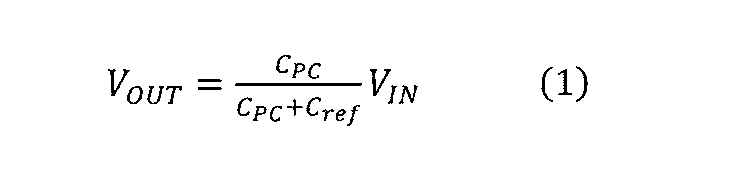
光電変換層25に光が入射すると、励起子の生成によって対向電極21eおよび画素電極22eにおける電荷密度が増大し、対向電極21eと画素電極22eとの間の容量値が変化する。つまり、光の照射によって容量値CPCが変化する。このとき、容量素子30の容量値Crefは、画素10Aaへの光の照射によってほとんど変化せず、光の照射による容量値Crefの変化は、容量値CPCの変化と比較して十分に小さいとする。この場合、ノードMの電圧VOUTは、誘電率変調構造26aの容量値CPCの変化に従って変化する。
When light is incident on the photoelectric conversion layer 25, the charge density in the counter electrode 21e and the pixel electrode 22e increases due to the generation of excitons, and the capacitance value between the counter electrode 21e and the pixel electrode 22e changes. That is, the capacitance value C PC changes due to the light irradiation. At this time, the capacitance value C ref of the capacitance element 30 hardly changes due to the light irradiation to the pixel 10Aa, and the change of the capacitance value C ref due to the light irradiation is sufficiently compared with the change of the capacitance value C PC It is assumed that it is small. In this case, the voltage V OUT of the node M changes in accordance with the change of the capacitance value C PC of the dielectric constant modulation structure 26 a.
図4は、VINとして5Vの電圧を印加し、Crefが1.2fFであるときの、容量値CPCの変化に対するVOUTの変化を示す。図4からわかるように、光の照射によって容量値CPCが増大することにより、第2端子22の電位であるVOUTの値も上昇する。したがって、ノードMに検出回路40を接続することにより、画素10Aaに対する照度の変化を、ソースフォロワとしての信号検出トランジスタ41への入力電圧の変化の形で検出可能である。なお、式(1)からわかるように、容量値CPCの初期値、例えば、光が照射されていない状態における誘電率変調構造26aの容量値CPCが容量値Crefに対して大きい値であると、光の照射による容量値CPCの増大に対する電圧VOUTの変化が小さくなる。そのため、容量素子30が容量値CPCの初期値に対して比較的大きな容量値を有することが有益である。
FIG. 4 shows a change in V OUT with respect to a change in capacitance value C PC when a voltage of 5 V is applied as V IN and C ref is 1.2 fF. As can be seen from FIG. 4, as the capacitance value CPC is increased by the light irradiation, the value of V OUT which is the potential of the second terminal 22 is also increased. Therefore, by connecting the detection circuit 40 to the node M, it is possible to detect a change in illuminance for the pixel 10Aa in the form of a change in input voltage to the signal detection transistor 41 as a source follower. As can be seen from the equation (1), the initial value of the capacitance value C PC , for example, the capacitance value C PC of the dielectric constant modulation structure 26 a in a state where light is not irradiated is larger than the capacitance value C ref . If so, the change in the voltage V OUT with respect to the increase of the capacitance value C PC due to the light irradiation becomes small. Therefore, it is beneficial to have a relatively large capacitance value to the capacitive element 30 is capacitance C PC initial value.
このように、本開示の実施形態によれば、光の照射による誘電率変調素子20の誘電率の変化を通して、光を検出することができる。さらに、本開示の実施形態では、光電変換によって生じた正孔または電子を信号電荷として取り出してその電荷量を読み出す構成とは異なり、誘電率変調素子20からは電荷を取り出さない。そのため、電圧供給回路50から誘電率変調素子20に印加する電圧を制御して、例えば、対向電極21eと画素電極22eとの間の電位差を0Vに近づける。そうすれば、誘電率変調構造26a中の正および負の電荷が速やかに再結合し、光の照射によって上昇していた誘電率変調構造26aの誘電率が低下する。すなわち、本開示の実施形態によれば、リセット電圧の供給によるリセット動作を基本的に不要とすることができる。
Thus, according to the embodiment of the present disclosure, light can be detected through the change of the dielectric constant of the dielectric constant modulation element 20 due to the irradiation of light. Furthermore, in the embodiment of the present disclosure, unlike the configuration in which holes or electrons generated by photoelectric conversion are taken out as signal charges and the charge amount is read out, charges are not taken out from the dielectric constant modulation element 20. Therefore, by controlling the voltage applied from the voltage supply circuit 50 to the dielectric constant modulation element 20, for example, the potential difference between the counter electrode 21e and the pixel electrode 22e approaches 0V. Then, the positive and negative charges in the dielectric constant modulation structure 26a quickly recombine, and the dielectric constant of the dielectric constant modulation structure 26a which has been raised by the light irradiation is lowered. That is, according to the embodiment of the present disclosure, the reset operation by the supply of the reset voltage can be basically eliminated.
(撮像装置の例示的な動作)
次に、本開示の実施形態による撮像装置の例示的な動作を説明する。図5は、本開示の実施形態による撮像装置の例示的な動作を説明するためのタイミングチャートである。図5中、最上段のグラフは、電圧供給回路50から電源線70に供給される電圧VINの変化を示し、真ん中のグラフは、アドレストランジスタ42のゲートに接続されたアドレス信号線の電位VSELの変化を示す。最下段のグラフは、AD変換回路62の駆動を制御するための電圧VADの変化を示す。 (Exemplary Operation of Imaging Device)
Next, exemplary operations of an imaging device according to embodiments of the present disclosure will be described. FIG. 5 is a timing chart to explain an exemplary operation of an imaging device according to an embodiment of the present disclosure. In FIG. 5, the uppermost graph shows the change of the voltage V IN supplied from thevoltage supply circuit 50 to the power supply line 70, and the middle graph shows the potential V of the address signal line connected to the gate of the address transistor 42. Indicates a change in SEL . The lowermost graph shows changes in the voltage VAD for controlling the drive of the AD conversion circuit 62.
次に、本開示の実施形態による撮像装置の例示的な動作を説明する。図5は、本開示の実施形態による撮像装置の例示的な動作を説明するためのタイミングチャートである。図5中、最上段のグラフは、電圧供給回路50から電源線70に供給される電圧VINの変化を示し、真ん中のグラフは、アドレストランジスタ42のゲートに接続されたアドレス信号線の電位VSELの変化を示す。最下段のグラフは、AD変換回路62の駆動を制御するための電圧VADの変化を示す。 (Exemplary Operation of Imaging Device)
Next, exemplary operations of an imaging device according to embodiments of the present disclosure will be described. FIG. 5 is a timing chart to explain an exemplary operation of an imaging device according to an embodiment of the present disclosure. In FIG. 5, the uppermost graph shows the change of the voltage V IN supplied from the
上述したように、電圧供給回路50は、少なくとも2つの異なる電圧を切り替えて可能な構成を有する。ここでは、電圧供給回路50が、ハイレベルの第1電圧および第1電圧よりも低いローレベルの第2電圧のいずれかを選択的に電源線70に供給可能であるとする。上述の式(1)からわかるように、検出回路40の信号検出トランジスタ41のゲートに印加される電圧VOUTは、誘電率変調素子20の第1端子21に印加される電圧VIN、換言すれば、電圧供給回路50が電源線70に印加する電圧に比例する。上述のように、誘電率変調構造26aの容量値CPCは、照度に応じて変化し、それに伴って電圧VOUTも変化するが、電圧VINが小さければ、照度の変化に伴う電圧VOUTの変化も小さい。図3に示すように、ここでは、容量素子30の、ノードMに接続されていない側の電極の電位が接地である。そのため、ローレベルの第2電圧が例えば接地、すなわち、0Vであるとすると、照度の如何にかかわらず、信号検出トランジスタ41のゲートに印加される電圧VOUTは、基本的には0Vとなる。したがって、電圧供給回路50がローレベルの第2電圧を電源線70に印加している期間が、非露光期間に相当するといえる。
As described above, the voltage supply circuit 50 has a configuration capable of switching at least two different voltages. Here, it is assumed that the voltage supply circuit 50 can selectively supply either the high level first voltage or the low level second voltage lower than the first voltage to the power supply line 70. As understood from the above-mentioned equation (1), the voltage V OUT applied to the gate of the signal detection transistor 41 of the detection circuit 40 is the voltage V IN applied to the first terminal 21 of the permittivity modulation element 20, in other words For example, the voltage supply circuit 50 is proportional to the voltage applied to the power supply line 70. As described above, the capacitance value C PC of the dielectric constant modulation structure 26a changes according to the illuminance, and the voltage V OUT also changes accordingly, but if the voltage V IN is small, the voltage V OUT accompanying the change of the illuminance Change is also small. As shown in FIG. 3, here, the potential of the electrode of the capacitive element 30 not connected to the node M is the ground. Therefore, assuming that the low level second voltage is, for example, ground, ie, 0 V, the voltage V OUT applied to the gate of the signal detection transistor 41 is basically 0 V regardless of the illuminance. Therefore, it can be said that the period in which the voltage supply circuit 50 applies the low level second voltage to the power supply line 70 corresponds to the non-exposure period.
図5に示す例では、初期の状態において、電源線70に第2電圧が印加されている。ここでは、第2電圧が0Vであるとする。
In the example shown in FIG. 5, the second voltage is applied to the power supply line 70 in the initial state. Here, it is assumed that the second voltage is 0V.
電圧供給回路50は、時刻t1において、電源線70に印加する電圧をハイレベルの第1電圧としている。誘電率変調素子20aの対向電極21eに印加される電圧VINが第1電圧とされることにより、式(1)および図4からわかるように、電圧VOUTは、照度に応じた容量値CPCの変化に伴って変化する。すなわち、照度に応じた電圧VOUTが信号検出トランジスタ41のゲートに印加された状態となる。
At time t1, the voltage supply circuit 50 sets the voltage applied to the power supply line 70 to the high level first voltage. As the voltage V IN applied to the counter electrode 21 e of the dielectric constant modulation element 20 a is made the first voltage, the voltage V OUT has a capacitance value C corresponding to the illuminance, as can be seen from the equation (1) and FIG. It changes with the change of PC . That is, the voltage V OUT corresponding to the illuminance is applied to the gate of the signal detection transistor 41.
次に、時刻t2においてアドレス信号線の電位VSELをハイレベルとし、アドレストランジスタ42をオンとする。アドレストランジスタ42がオンとされることにより、選択された画素10Aの検出回路40から、照度に応じた信号が出力信号線74に出力される。この例では、照度に応じた電圧信号が出力信号線74に出力される。
Next, at time t2, the potential V SEL of the address signal line is set to the high level, and the address transistor 42 is turned on. When the address transistor 42 is turned on, a signal corresponding to the illuminance is output from the detection circuit 40 of the selected pixel 10A to the output signal line 74. In this example, a voltage signal corresponding to the illuminance is output to the output signal line 74.
図5に示す例において、時刻t3にAD変換回路62の駆動パルスが立ち上げられている。すなわち、電圧供給回路50が電源線70にハイレベルの第1電圧を供給し、かつ、アドレストランジスタ42がオンとされた状態で、AD変換回路62が動作されている。AD変換回路62の動作によってこのときに得られるデジタル値が、この例における、照度に応じた画素信号である。
In the example shown in FIG. 5, the drive pulse of the AD conversion circuit 62 is raised at time t3. That is, the AD conversion circuit 62 is operated in a state where the voltage supply circuit 50 supplies the high-level first voltage to the power supply line 70 and the address transistor 42 is turned on. The digital value obtained at this time by the operation of the AD conversion circuit 62 is the pixel signal corresponding to the illuminance in this example.
次に、時刻t4において、電圧供給回路50は、電源線70に供給する電圧をローレベルの第2電圧に切り替えている。電源線70に供給される電圧が第2電圧に切り替えられることにより、対向電極21eと画素電極22eとの間の電位差が縮小し、光の照射によって光電変換層25内に生成された正および負の電荷の対が速やかに再結合する。特に、ここでは、第2電圧が0Vとされているので、電圧VOUTが0Vとなる。つまり、信号検出トランジスタ41のゲートに印加される電圧VOUTが、電源線70にハイレベルの第1電圧が供給される前の状態に戻る。すなわち、本開示の実施形態では、各画素10Aに対して電圧供給回路50が相対的に高い電圧を供給している期間を露光期間とみなすことができる。図5中の両矢印EXPは、この露光期間を模式的に表現している。
Next, at time t4, the voltage supply circuit 50 switches the voltage supplied to the power supply line 70 to the low level second voltage. By switching the voltage supplied to the power supply line 70 to the second voltage, the potential difference between the counter electrode 21 e and the pixel electrode 22 e is reduced, and positive and negative generated in the photoelectric conversion layer 25 by light irradiation. The pair of charges quickly recombine. In particular, here, since the second voltage is 0V, the voltage V OUT is 0V. That is, the voltage V OUT applied to the gate of the signal detection transistor 41 returns to the state before the high level first voltage is supplied to the power supply line 70. That is, in the embodiment of the present disclosure, a period in which the voltage supply circuit 50 supplies a relatively high voltage to each pixel 10A can be regarded as an exposure period. The double arrow EXP in FIG. 5 schematically represents this exposure period.
電源線70に供給される電圧が第2電圧に切り替えられた後、時刻t5において、AD変換回路62の駆動パルスが再び立ち上げられる。AD変換回路62の動作により、電源線70にハイレベルの第1電圧が供給される前の基準レベルの信号に相当するデジタル値が得られる。電源線70に第2電圧が供給されている第2期間に読み出しを実行することにより、照度の大小の影響を受けずに基準レベルの信号を読み出すことが可能である。
After the voltage supplied to the power supply line 70 is switched to the second voltage, at time t5, the drive pulse of the AD conversion circuit 62 is raised again. By the operation of the AD conversion circuit 62, a digital value corresponding to the signal of the reference level before the high level first voltage is supplied to the power supply line 70 is obtained. By reading out in the second period in which the power supply line 70 is supplied with the second voltage, it is possible to read out the signal of the reference level without being affected by the magnitude of the illuminance.
信号処理回路60は、時刻t3に得られたデジタル値と、時刻t5に得られたデジタル値との差分を生成して出力する。すなわち、信号処理回路60は、被写体の照度を示す信号として、電源線70にハイレベルの第1電圧が供給されている期間に得られた画素信号と、電源線70にローレベルの第2電圧が供給されている期間に得られた基準レベルの信号との差分を生成する。その後、時刻t6においてアドレストランジスタ42がオフとされる。
The signal processing circuit 60 generates and outputs the difference between the digital value obtained at time t3 and the digital value obtained at time t5. That is, the signal processing circuit 60 generates a pixel signal obtained during a period in which the first voltage of high level is supplied to the power supply line 70 as a signal indicating the illuminance of the object, and a second voltage of low level to the power supply line 70. Generates a difference with the signal of the reference level obtained during the period in which Thereafter, at time t6, the address transistor 42 is turned off.
電圧供給回路50が第1端子21に対して第1電圧を印加する第1の期間と、第1電圧とは異なる第2電圧を印加する第2の期間とのそれぞれについて検出回路40によって電圧VOUTを検出し、各期間の検出回路40の出力の差分を取る。このようにして得られた信号成分は、第1端子21にハイレベルの電圧が印加されているときに得られた信号成分を、被写体の照度を示す信号としてそのまま出力する場合と比較して、ノイズ成分が抑えられている。なお、画素信号の検出と、基準レベルの信号の検出の順序は、図5に示す例に限定されず、基準レベルの信号の検出を先に実行してもよい。また、検出回路40の出力の差分も、デジタル値同士の差分の形に限定されず、例えば、アナログ波形の振幅の差分の形であってもよい。
The voltage V by the detection circuit 40 in each of a first period in which the voltage supply circuit 50 applies a first voltage to the first terminal 21 and a second period in which a second voltage different from the first voltage is applied. OUT is detected, and the difference of the output of the detection circuit 40 in each period is taken. The signal component thus obtained is compared with the case where the signal component obtained when a high level voltage is applied to the first terminal 21 is directly output as a signal indicating the illuminance of the object, The noise component is suppressed. The order of the detection of the pixel signal and the detection of the signal of the reference level is not limited to the example shown in FIG. 5, and the detection of the signal of the reference level may be performed first. Also, the difference between the outputs of the detection circuit 40 is not limited to the form of the difference between the digital values, and may be, for example, the form of the difference between the amplitudes of the analog waveforms.
図6は、複数のフレームにわたる撮像動作の一例を示す。図6に示す例では、まず、電圧供給回路50から電源線70に印加される電圧が、時刻t11においてハイレベルの第1電圧とされている。電圧供給回路50による第1電圧の印加の開始が、0番目のフレーム期間の露光期間の開始に相当する。所定の期間の経過後、例えば時刻t12にアドレストランジスタ42をオンとする。さらに、時刻t13においてAD変換回路62を動作させることにより、照度に応じた画素信号が得られる。
FIG. 6 shows an example of an imaging operation over a plurality of frames. In the example shown in FIG. 6, first, the voltage applied from the voltage supply circuit 50 to the power supply line 70 is set to the high level first voltage at time t11. The start of the application of the first voltage by the voltage supply circuit 50 corresponds to the start of the exposure period of the 0th frame period. After a predetermined period, for example, the address transistor 42 is turned on at time t12. Further, by operating the AD conversion circuit 62 at time t13, a pixel signal according to the illuminance can be obtained.
照度に応じた画素信号を得た後、時刻t14において、電圧供給回路50から電源線70に印加される電圧が、ローレベルの第2電圧に切り替えられる。図5を参照して説明したように、第2電圧への切り替えのタイミングが、0番目のフレーム期間における露光期間の終了に相当する。
After obtaining the pixel signal according to the illuminance, at time t14, the voltage applied from the voltage supply circuit 50 to the power supply line 70 is switched to the low level second voltage. As described with reference to FIG. 5, the timing of switching to the second voltage corresponds to the end of the exposure period in the zeroth frame period.
次に、電圧供給回路50から第2電圧が供給されている状態で、時刻t15において再びAD変換回路62が動作され、基準レベルの信号が取得される。その後、時刻t16にアドレストランジスタ42がオフとされ、0番目のフレーム期間が終了する。信号処理回路60は、被写体の照度を示す信号として、画素信号と、時刻t15に得られた基準レベルの信号との差分を生成する。
Next, in a state where the second voltage is supplied from the voltage supply circuit 50, the AD conversion circuit 62 is operated again at time t15, and a signal of the reference level is acquired. Thereafter, at time t16, the address transistor 42 is turned off, and the 0th frame period ends. The signal processing circuit 60 generates a difference between the pixel signal and the signal of the reference level obtained at time t15 as a signal indicating the illuminance of the subject.
その後、時刻t21に、電圧供給回路50が電源線70に印加する電圧を再びハイレベルの第1電圧に切り替えることにより、次のフレーム期間、すなわち、1番目のフレーム期間が開始される。
Thereafter, at time t21, the voltage applied by the voltage supply circuit 50 to the power supply line 70 is again switched to the high level first voltage, whereby the next frame period, that is, the first frame period is started.
1番目のフレーム期間の開始後、時刻t22にアドレストランジスタ42がオンとされ、時刻t23にAD変換回路62が動作させられることにより、1番目のフレームに関する、照度に応じた画素信号が取得される。
After the start of the first frame period, the address transistor 42 is turned on at time t22, and the AD conversion circuit 62 is operated at time t23 to acquire a pixel signal corresponding to the illuminance for the first frame. .
1番目のフレームに関する画素信号の取得後、この例では、時刻t24に、電源線70に印加される電圧がローレベルの第2電圧に切り替えられるとともに、アドレストランジスタ42がオフとされている。さらに、基準レベルの信号の取得が実行されることなく、電源線70に印加される電圧が、時刻t31において再び第1電圧に切り替えられている。換言すれば、2番目のフレーム期間が開始されている。
After obtaining the pixel signal for the first frame, in this example, at time t24, the voltage applied to the power supply line 70 is switched to the low level second voltage, and the address transistor 42 is turned off. Furthermore, the voltage applied to the power supply line 70 is switched to the first voltage again at time t31 without acquiring the signal of the reference level. In other words, the second frame period has begun.
ここで、信号処理回路60は、被写体の照度を示す信号として、時刻t23に得られた画素信号と、0番目のフレーム期間中の時刻t15に得られた基準レベルの信号との差分を生成する。本開示の典型的な実施形態によれば、第1端子21に印加する電圧VINを初期状態に戻すことにより、換言すれば、電圧供給回路50が電源線70に印加する電圧をローレベルの第2電圧に戻すことにより、誘電率変調素子20の状態を、光を照射する前の状態に戻し得る。つまり、画素にリセット電圧を供給することによるリセット動作を実行せずとも、ノードMの電位を実質的にリセットすることが可能である。そのため、リセット動作に伴うリセットノイズの混入を回避でき、リセットノイズの混入による、フレーム間の基準レベルの変動を回避することができる。これは、低照度の場合にSN比を確保する観点からは、特に有利な点である。フレーム間の基準レベルの変動が生じないので、連続するフレーム期間の最初のフレーム期間に基準レベルの信号を一度取得しておけば、その後のフレーム期間についてもその基準レベルの信号を使いまわすことが可能である。
Here, the signal processing circuit 60 generates a difference between the pixel signal obtained at time t23 and the signal of the reference level obtained at time t15 in the 0th frame period as a signal indicating the illuminance of the subject. . According to an exemplary embodiment of the present disclosure, the voltage V IN applied to the first terminal 21 is returned to the initial state, in other words, the voltage applied by the voltage supply circuit 50 to the power supply line 70 is low. By returning to the second voltage, the state of the dielectric constant modulation element 20 can be returned to the state before the light irradiation. That is, the potential of the node M can be substantially reset without executing the reset operation by supplying the reset voltage to the pixel. Therefore, it is possible to avoid the introduction of reset noise accompanying the reset operation, and to avoid the fluctuation of the reference level between frames due to the introduction of the reset noise. This is a particularly advantageous point from the viewpoint of securing the SN ratio in the case of low illuminance. Since there is no fluctuation of reference level between frames, if a signal of reference level is acquired once in the first frame period of consecutive frame periods, the signal of the reference level may be used for the subsequent frame periods as well. It is possible.
続く2番目のフレーム期間における動作も、1番目のフレーム期間における動作と同様であり得る。この例では、時刻t32にアドレストランジスタ42をオンとし、時刻t33にAD変換回路62を動作させて、2番目のフレームに関する、照度に応じた画素信号を取得している。画素信号の取得後、時刻t34に電圧VINを第2電圧に切り替え、アドレストランジスタ42をオフとすることにより、2番目のフレーム期間が終了する。信号処理回路60が、被写体の照度を示す信号として、時刻t33に得られた画素信号と、0番目のフレーム期間中に得られた基準レベルの信号との差分を生成する点は、1番目のフレームと同様である。
The operation in the subsequent second frame period may be similar to the operation in the first frame period. In this example, the address transistor 42 is turned on at time t32, and the AD conversion circuit 62 is operated at time t33 to obtain a pixel signal corresponding to the illuminance for the second frame. After acquisition of the pixel signal, the voltage V IN is switched to the second voltage at time t34 and the address transistor 42 is turned off, whereby the second frame period ends. The point that the signal processing circuit 60 generates a difference between the pixel signal obtained at time t33 and the signal of the reference level obtained in the 0th frame period as a signal indicating the illuminance of the object is the first point. It is similar to the frame.
このように、連続する2以上のフレーム期間において、電圧供給回路50が各画素10Aに第2電圧を供給している期間に検出回路40を介して信号が読み出される回数は、電圧供給回路50が第1電圧を供給している期間に検出回路40を介して信号が読み出される回数よりも少ないことがあり得る。すなわち、基準レベルの信号の読み出しの回数が、照度に応じた画素信号の読み出しの回数よりも少なくてもよい。このような動作によれば、フレーム期間ごとの基準レベルの信号の取得が省略されるので、信号の読み出しに要する期間を短縮して高速に撮像を実行し得る。あるいは、フレーム期間ごとの基準レベルの信号の取得を省略した分、露光時間を長くすることができ、より高いSN比を実現可能である。
As described above, in the two or more consecutive frame periods, the number of times the voltage supply circuit 50 reads the signal through the detection circuit 40 during the period in which the voltage supply circuit 50 supplies the second voltage to each pixel 10A. It may be less than the number of times the signal is read out through the detection circuit 40 during the period of supplying the first voltage. That is, the number of times of reading of the signal of the reference level may be smaller than the number of times of reading of the pixel signal according to the illuminance. According to such an operation, since acquisition of the signal of the reference level for each frame period is omitted, the period required for signal readout can be shortened and imaging can be performed at high speed. Alternatively, the exposure time can be lengthened by omitting the acquisition of the signal of the reference level for each frame period, and a higher SN ratio can be realized.
図7は、2次元に配列された複数の画素を含む撮像装置の読み出し動作の一例を模式的に示す。図7中、最上段の白い矩形Hは、電圧供給回路50が第1端子21にハイレベルの第1電圧を印加する第1期間を表現し、ハッチングの付された矩形Lは、電圧供給回路50が第1端子21にローレベルの第2電圧を印加する第2期間を表現している。なお、ここでは、各画素10Aaの対向電極21eに共通の電圧が印加されるとしている。
FIG. 7 schematically illustrates an example of the read operation of the imaging device including a plurality of pixels arranged in two dimensions. In FIG. 7, the white rectangle H in the top row represents the first period during which the voltage supply circuit 50 applies the first voltage of high level to the first terminal 21, and the hatched rectangle L represents the voltage supply circuit. 50 represents a second period in which a low level second voltage is applied to the first terminal 21. Here, a common voltage is applied to the counter electrode 21e of each pixel 10Aa.
図7では、簡単のため、複数の行のうち、第i行に属する画素、第(i+1)行に属する画素、および、第(i+2)行に属する画素の動作を代表して示している。図7中、白い矩形Expは、各行における露光期間を表現し、網掛けの矩形Rdは、信号の読み出し期間を表現している。ここでは、矩形Rdで表されたタイミングで、画素信号の読み出しと基準レベルの信号の読み出しとを実行する。画素信号の読み出しは、第1期間に実行され、基準レベルの信号の読み出しは、第2期間に実行される。上述したように、本開示の実施形態によれば、フレーム期間ごとの基準レベルの信号の取得を省略し得る。この例では、画素信号および基準レベルの信号の読み出しを行単位でタイミングをずらして順次に実行している。
For the sake of simplicity, FIG. 7 representatively shows operations of a pixel belonging to the i-th row, a pixel belonging to the (i + 1) -th row, and a pixel belonging to the (i + 2) -th row among a plurality of rows. In FIG. 7, white rectangles Exp represent exposure periods in each row, and shaded rectangles Rd represent signal readout periods. Here, the readout of the pixel signal and the readout of the signal of the reference level are executed at the timing represented by the rectangle Rd. The readout of the pixel signal is performed in the first period, and the readout of the signal of the reference level is performed in the second period. As mentioned above, according to the embodiments of the present disclosure, acquisition of a signal of a reference level for each frame period may be omitted. In this example, readout of the pixel signal and the signal of the reference level is sequentially performed while shifting the timing on a row basis.
図8は、2次元に配列された複数の画素を含む撮像装置の読み出し動作の他の一例を模式的に示す。図8中、網掛けの矩形Rd1は、画素信号の読み出し期間を表現し、網掛けの矩形Rd2は、基準レベルの信号の読み出し期間を表現している。この例では、第1期間において画素信号の読み出しを行単位で順次に実行し、また、第2期間において基準レベルの信号の読み出しを行単位で順次に実行している。この例のように、1フレーム期間に、第1電圧から第2電圧への電圧切り替えと、第2電圧から第1の電圧への切り替えとを1回ずつ行うようにしてもよい。
FIG. 8 schematically shows another example of the readout operation of the imaging device including a plurality of pixels arranged in a two-dimensional manner. In FIG. 8, the shaded rectangle Rd1 represents the readout period of the pixel signal, and the shaded rectangle Rd2 represents the readout period of the signal of the reference level. In this example, readout of pixel signals is sequentially performed in row units in a first period, and readout of signals of a reference level is sequentially performed in row units in a second period. As in this example, voltage switching from the first voltage to the second voltage and switching from the second voltage to the first voltage may be performed once in one frame period.
図9および図10は、2次元に配列された複数の画素を含む撮像装置の読み出し動作のさらに他の一例を模式的に示す。図9に示す例では、各フレーム期間において、全ての行について共通のタイミングで信号の読み出しを実行しており、露光期間の開始および終了が全ての画素に共通となっている。すなわち、いわゆるグローバルシャッタが実現されている。
FIG. 9 and FIG. 10 schematically show still another example of the readout operation of the imaging device including a plurality of pixels arranged in two dimensions. In the example shown in FIG. 9, in each frame period, signal readout is performed at common timing for all the rows, and the start and end of the exposure period are common to all the pixels. That is, a so-called global shutter is realized.
このような読み出し動作は、撮像領域が形成されたチップとは別のチップに信号処理回路60と、撮像領域中の特定の画素を指定するXYデコーダとを配置し、例えばこれらのチップを積層して複数の画素の各行と信号処理回路60とを電気的に接続することによって実現可能である。各画素にアナログ-デジタル変換回路を配置してもよい。チップ積層技術によれば、画素の大型化を回避しながら、このような読み出し方式に適合した撮像装置を実現し得る。
In such a reading operation, the signal processing circuit 60 and an XY decoder for designating a specific pixel in the imaging area are arranged on a chip different from the chip in which the imaging area is formed. For example, these chips are stacked. This can be realized by electrically connecting each row of a plurality of pixels to the signal processing circuit 60. An analog-digital conversion circuit may be arranged in each pixel. According to the chip stacking technology, it is possible to realize an imaging device adapted to such a reading method while avoiding an increase in size of a pixel.
図10に示す例でも同様に、露光期間の開始および終了が全ての画素に共通とされている。図10は、フレームメモリを有する画素に適用可能な動作例である。図10中、網掛けの矩形Trsは、信号レベルに関する情報をフレームメモリに転送する期間を表現している。図10は、露光期間に得られた画素信号の電圧レベルをフレームメモリに転送しておき、次のフレーム期間の露光期間中に画素信号の電圧レベルをフレームメモリから読み出す例である。なお、基準レベルの信号の読み出しは、いずれかのフレーム期間中の第2期間に実行されればよい。
Similarly in the example shown in FIG. 10, the start and end of the exposure period are common to all the pixels. FIG. 10 shows an operation example applicable to a pixel having a frame memory. In FIG. 10, a shaded rectangle Trs represents a period for transferring information on the signal level to the frame memory. FIG. 10 shows an example in which the voltage level of the pixel signal obtained in the exposure period is transferred to the frame memory, and the voltage level of the pixel signal is read out from the frame memory during the exposure period of the next frame period. Note that the reading of the signal of the reference level may be performed in the second period in any frame period.
図11は、フレームメモリを有する画素の例を示す。図11に示す画素10Bは、ノードMと信号検出トランジスタ41のゲートの間に接続された転送トランジスタ45と、一方の電極が信号検出トランジスタ41のゲートに接続された容量素子44との組を含む。容量素子44の他方の電極は、例えば不図示の電源に接続されることにより、撮像装置100Aの動作時に所定の電圧VGを印加可能に構成される。
FIG. 11 shows an example of a pixel having a frame memory. The pixel 10B shown in FIG. 11 includes a set of a transfer transistor 45 connected between the node M and the gate of the signal detection transistor 41, and a capacitive element 44 having one electrode connected to the gate of the signal detection transistor 41. . The other electrode of the capacitor 44, for example by being connected to a power supply (not shown), capable of applying configured the predetermined voltage V G during operation of the imaging apparatus 100A.
第1期間の開始から所定の期間の経過後に転送トランジスタ45をオンとし、再びオフとすることにより、露光後のノードMの電圧レベルを容量素子44によって一時的に保持することができる。電圧レベルを容量素子44に保持させた後は、アドレストランジスタ42をオンとすることにより、容量素子44に保持させた電圧レベルに対応する信号を所望のタイミングで出力信号線74に読み出すことができる。転送トランジスタ45のおよびオフは、例えば、不図示の行走査回路によって制御され得る。なお、高感度化の観点から、容量素子44が、容量素子30(例えば、不純物領域30a)の容量値よりも小さな容量値を有すると有益である。
The voltage level of the node M after exposure can be temporarily held by the capacitive element 44 by turning on the transfer transistor 45 after the lapse of a predetermined period from the start of the first period and turning it off again. After the voltage level is held in the capacitive element 44, a signal corresponding to the voltage level held in the capacitive element 44 can be read out to the output signal line 74 at a desired timing by turning on the address transistor 42. . The transfer transistor 45 and off can be controlled, for example, by a row scanning circuit (not shown). From the viewpoint of increasing sensitivity, it is useful that the capacitive element 44 have a capacitance value smaller than that of the capacitive element 30 (for example, the impurity region 30a).
(オフセットレベルの除去)
上述したように、本開示の実施形態によれば、第1端子21と第2端子22との間の電位差を0Vに近づけることにより、光の照射の如何にかかわらずノードMの電位をほぼ0Vとできるので、一般的な撮像装置に要求されるリセット動作は、基本的に不要である。ただし、例えば、容量素子30の電極のうち、ノードMに接続されていない側の電極に与えられる電圧と、電圧供給回路50が誘電率変調素子20に印加する第2電圧とが一致していないとする。このような場合においては、誘電率変調素子20に印加される電圧が第1電圧に切り替えられると、光が照射されていなくても、ノードMの電位が0Vから上昇し得る。電圧供給回路50から対向電極21eに印加される第2電圧と、容量素子30の電極のうち、ノードMに接続されていない側に与えられる電圧との間の差分をΔV、暗時における誘電率変調構造26aの容量値をCiniとすれば、第1電圧に切り替えによって生じる、電圧VOUTのオフセットVoffsetは、下記の式(2)で与えられる。 (Remove offset level)
As described above, according to the embodiment of the present disclosure, by bringing the potential difference between thefirst terminal 21 and the second terminal 22 closer to 0 V, the potential of the node M is substantially 0 V regardless of light irradiation. Therefore, the reset operation required for a general imaging device is basically unnecessary. However, for example, the voltage applied to the electrode on the side not connected to the node M among the electrodes of the capacitive element 30 and the second voltage applied to the dielectric constant modulation element 20 by the voltage supply circuit 50 do not match. I assume. In such a case, when the voltage applied to the dielectric constant modulation element 20 is switched to the first voltage, the potential of the node M can rise from 0 V even without light irradiation. The difference between the second voltage applied from the voltage supply circuit 50 to the counter electrode 21e and the voltage applied to the side not connected to the node M of the electrodes of the capacitive element 30 is ΔV, the permittivity in dark Assuming that the capacitance value of the modulation structure 26 a is C ini , the offset V offset of the voltage V OUT generated by switching to the first voltage is given by the following equation (2).
上述したように、本開示の実施形態によれば、第1端子21と第2端子22との間の電位差を0Vに近づけることにより、光の照射の如何にかかわらずノードMの電位をほぼ0Vとできるので、一般的な撮像装置に要求されるリセット動作は、基本的に不要である。ただし、例えば、容量素子30の電極のうち、ノードMに接続されていない側の電極に与えられる電圧と、電圧供給回路50が誘電率変調素子20に印加する第2電圧とが一致していないとする。このような場合においては、誘電率変調素子20に印加される電圧が第1電圧に切り替えられると、光が照射されていなくても、ノードMの電位が0Vから上昇し得る。電圧供給回路50から対向電極21eに印加される第2電圧と、容量素子30の電極のうち、ノードMに接続されていない側に与えられる電圧との間の差分をΔV、暗時における誘電率変調構造26aの容量値をCiniとすれば、第1電圧に切り替えによって生じる、電圧VOUTのオフセットVoffsetは、下記の式(2)で与えられる。 (Remove offset level)
As described above, according to the embodiment of the present disclosure, by bringing the potential difference between the

このような電圧のオフセットが存在する場合、光の照射による誘電率の変化分に対応する本来の出力は、オフセット分を差し引いた下記の式(3)で与えられることになる。
When such a voltage offset exists, the original output corresponding to the change of the dielectric constant due to the light irradiation is given by the following equation (3) from which the offset is subtracted.

つまり、画素信号と基準レベルの信号との差分から上述のオフセットレベルに対応する信号をさらに差し引くことにより、初期状態においてノードMに蓄積されている電荷量の如何によらずに、光の照射による誘電率の変化に相当する実効的な電圧レベルの変化を取得することができる。例えば、信号処理回路60は、電源線70にハイレベルの第1電圧が供給されている期間に得られた画素信号と、電源線70にローレベルの第2電圧が供給されている期間に得られた基準レベルの信号との差分から、オフセットレベルに対応する信号をさらに減算した信号を、被写体の照度を示す信号として出力してもよい。オフセットレベルに対応する信号の減算は、デジタル信号同士の減算の形で実行されてもよいし、アナログ信号同士の減算の形で実行されてもよい。オフセットレベルに対応する信号の減算により、画素ごとのオフセットレベルのバラつきに起因する固定パターンノイズを低減することが可能である。
That is, by further subtracting the signal corresponding to the above-mentioned offset level from the difference between the pixel signal and the signal of the reference level, the irradiation of light is performed regardless of the amount of charge stored in node M in the initial state. Changes in the effective voltage level corresponding to changes in the dielectric constant can be obtained. For example, the signal processing circuit 60 may obtain the pixel signal obtained during the period in which the first voltage of high level is supplied to the power supply line 70 and the period during which the second voltage of low level is supplied to the power supply line 70. A signal obtained by further subtracting the signal corresponding to the offset level from the difference from the signal of the reference level may be output as a signal indicating the illuminance of the subject. The subtraction of the signal corresponding to the offset level may be performed in the form of subtraction of digital signals or may be performed in the form of subtraction of analog signals. By subtracting the signal corresponding to the offset level, it is possible to reduce fixed pattern noise due to the variation of the offset level for each pixel.
(オフセットレベルに対応する信号の取得)
オフセットレベルに対応する信号は、誘電率変調素子20に光が照射されておらず、かつ、電圧供給回路50から電源線70にハイレベルの第1電圧が供給されている状態において検出回路40が出力する信号である。以下に説明するように、オフセットレベルに対応する信号は、種々の方法により取得可能である。 (Acquisition of signal corresponding to offset level)
The signal corresponding to the offset level is not irradiated with light to the dielectricconstant modulation element 20, and the detection circuit 40 is in a state in which the high-level first voltage is supplied from the voltage supply circuit 50 to the power supply line 70. It is a signal to be output. As described below, the signal corresponding to the offset level can be obtained by various methods.
オフセットレベルに対応する信号は、誘電率変調素子20に光が照射されておらず、かつ、電圧供給回路50から電源線70にハイレベルの第1電圧が供給されている状態において検出回路40が出力する信号である。以下に説明するように、オフセットレベルに対応する信号は、種々の方法により取得可能である。 (Acquisition of signal corresponding to offset level)
The signal corresponding to the offset level is not irradiated with light to the dielectric
図12は、オフセットレベルに対応する信号を取得可能な構成の第1の例を示す。図12に例示する構成において、撮像装置は、上述の画素10Aaに加えてダミー画素10Dmを含む複数の画素の配列を有する。ダミー画素10Dmにおいて、遮光層28は、誘電率変調素子20aを覆い、誘電率変調素子20aへの光の入射を遮断する。ダミー画素10Dmの基本的なデバイス構造は、遮光層28を有する点を除き、画素10Aaと同様である。なお、ダミー画素10Dmの誘電率変調素子20aへの光の入射は不要であるので、図12に示すように、ダミー画素10Dmでは光学フィルタ86およびマイクロレンズ88は省略され得る。
FIG. 12 shows a first example of a configuration capable of acquiring a signal corresponding to the offset level. In the configuration illustrated in FIG. 12, the imaging device has an array of a plurality of pixels including a dummy pixel 10Dm in addition to the above-described pixel 10Aa. In the dummy pixel 10Dm, the light shielding layer 28 covers the dielectric constant modulation element 20a and blocks the incidence of light on the dielectric constant modulation element 20a. The basic device structure of the dummy pixel 10Dm is similar to that of the pixel 10Aa except that it has the light shielding layer 28. In addition, since incidence | injection of the light to the dielectric constant modulation element 20a of dummy pixel 10Dm is unnecessary, as shown in FIG. 12, the optical filter 86 and the micro lens 88 can be abbreviate | omitted in dummy pixel 10Dm.
ダミー画素10Dmの誘電率変調素子20aへの光の入射は、遮光層28によって防止されている。したがって、対向電極21eに第1電圧が印加された状態にあるダミー画素10Dmの検出回路40の出力を読み出すことにより、比較的簡易な構成によって、オフセットレベルに対応する信号を得ることができる。このようなダミー画素10Dmは、画素10Aaの配列から形成される撮像領域の外側の周辺領域に配置され得る。特に、画素ごとのオフセットレベルのバラつきの影響が小さい場合に、このような構成が有効である。
Incident of light to the dielectric constant modulation element 20 a of the dummy pixel 10 Dm is prevented by the light shielding layer 28. Therefore, by reading out the output of the detection circuit 40 of the dummy pixel 10Dm in the state where the first voltage is applied to the counter electrode 21e, a signal corresponding to the offset level can be obtained with a relatively simple configuration. Such dummy pixels 10Dm may be arranged in the peripheral area outside the imaging area formed from the array of the pixels 10Aa. Such a configuration is effective particularly when the influence of the variation in the offset level for each pixel is small.
図13は、オフセットレベルに対応する信号を取得可能な構成の第2の例を示す。図13に例示する構成において、撮像装置は、各画素10Aaへの光の入射および遮断を切り替えるメカニカルシャッタ110を有している。
FIG. 13 shows a second example of a configuration capable of acquiring a signal corresponding to the offset level. In the configuration illustrated in FIG. 13, the imaging device has a mechanical shutter 110 that switches the incidence and blocking of light to each pixel 10Aa.
対向電極21eに第1電圧が印加された状態でメカニカルシャッタ110をオープンとすれば、検出回路40を介して画素信号が得られる。他方、対向電極21eに第1電圧が印加された状態、かつ、メカニカルシャッタ110がクローズとされた状態で検出回路40からの出力を取得することにより、オフセットレベルに対応する信号を得ることができる。このように、信号処理回路60と同期して動作するメカニカルシャッタ110を利用してオフセットレベルに対応する信号を取得してもよい。ここで説明した第2の例によれば、画素ごとにオフセットレベルが異なっていたとしても、正確にオフセットを求めることが可能である。
If the mechanical shutter 110 is opened in a state where the first voltage is applied to the counter electrode 21 e, a pixel signal can be obtained through the detection circuit 40. On the other hand, a signal corresponding to the offset level can be obtained by acquiring the output from the detection circuit 40 in a state in which the first voltage is applied to the counter electrode 21e and in a state in which the mechanical shutter 110 is closed. . As described above, the mechanical shutter 110 that operates in synchronization with the signal processing circuit 60 may be used to obtain a signal corresponding to the offset level. According to the second example described here, even if the offset level is different for each pixel, it is possible to accurately obtain the offset.
図14は、オフセットレベルに対応する信号を取得可能な構成の第3の例を示す。図14に示す撮像装置100Bは、光源120と、光源120および複数の画素10Aaを同期して駆動させる制御回路130とを含む。光源120は、対向電極21eにハイレベルの第1電圧が印加されている第1期間に、所定の波長域の光、例えば、赤外線で被写体Obを照射する。複数の画素10Aaは、被写体Obからの所定の波長域の反射光に基づく信号を出力する。
FIG. 14 shows a third example of the configuration capable of acquiring a signal corresponding to the offset level. An imaging device 100B illustrated in FIG. 14 includes a light source 120 and a control circuit 130 that synchronously drives the light source 120 and the plurality of pixels 10Aa. The light source 120 irradiates the object Ob with light of a predetermined wavelength range, for example, infrared light, in the first period in which the high level first voltage is applied to the counter electrode 21 e. The plurality of pixels 10Aa output a signal based on the reflected light of a predetermined wavelength range from the subject Ob.
このような構成においては、光源120が消灯状態かつ対向電極21eにハイレベルの第1電圧が印加された状態で画素10Aaの検出回路40によって検出される信号が、オフセットレベルに対応する信号に相当する。特定の波長域の光に基づく画像を得ようとする場合には、図14に例示するような構成も有用である。
In such a configuration, the signal detected by the detection circuit 40 of the pixel 10Aa in a state in which the light source 120 is turned off and the first voltage of high level is applied to the counter electrode 21e corresponds to the signal corresponding to the offset level. Do. When an image based on light of a specific wavelength range is to be obtained, the configuration as illustrated in FIG. 14 is also useful.
図14に例示するような構成は、特に、環境光に含まれる強度が小さい波長域の光の検出を行う場合に有用である。例えば、屋内での撮影においては900nm超、屋外での撮影であれば1400nm程度の波長を有する赤外線を光源120から発せられる光として利用することができる。光源120から発せられる光の波長が環境光のスペクトルに含まれていない場合には、光源120が消灯状態かつ対向電極21eにハイレベルの第1電圧が印加された状態で各画素10Aaの検出回路40によって検出される信号は、オフセットレベルに対応する信号の正確な値を与える。
The configuration as illustrated in FIG. 14 is particularly useful when detecting light in a wavelength range in which the intensity included in ambient light is small. For example, infrared light having a wavelength of about 900 nm or more for indoor photographing and about 1400 nm for outdoor photographing can be used as light emitted from the light source 120. When the wavelength of the light emitted from the light source 120 is not included in the spectrum of the ambient light, the detection circuit of each pixel 10Aa in the state where the light source 120 is turned off and the first voltage of high level is applied to the counter electrode 21e. The signal detected by 40 gives the correct value of the signal corresponding to the offset level.
これら第1~第3の例は、いずれも、オフセットレベルに対応する信号として、暗時の信号レベルに相当する出力を利用する例である。あるいは、オフセットレベルに対応する信号の取得に特化した構造を設けることなく、オフセットレベルに対応する信号を得ることも可能である。例えば、電圧供給回路50が電源線70に印加する電圧をローレベルの第2電圧からハイレベルの第1電圧に切り替えた直後、換言すれば、露光期間に相当する第1期間のごく初期に検出回路40から出力される信号を、オフセットレベルに対応する信号として取得してもよい。この例においても、各画素に応じたオフセットレベルを取得可能である。
All of the first to third examples are examples in which an output corresponding to the signal level in the dark is used as a signal corresponding to the offset level. Alternatively, it is possible to obtain the signal corresponding to the offset level without providing a structure specialized for obtaining the signal corresponding to the offset level. For example, immediately after the voltage supply circuit 50 switches the voltage applied to the power supply line 70 from the low level second voltage to the high level first voltage, in other words, detection is performed at the very beginning of the first period corresponding to the exposure period. The signal output from the circuit 40 may be acquired as a signal corresponding to the offset level. Also in this example, an offset level corresponding to each pixel can be obtained.
このように、画素ごとのオフセットレベルに対応する信号を画素信号の読み出しとは別のタイミングで一度読み出してもよい。また、暗時の条件で予め画素ごとにノードMの電位を求めておき、このときに得られた電位に対応する信号を、オフセットレベルに対応する信号として用いてもよい。また、信号処理回路60にメモリを設け、メモリ内にオフセットレベルの値を予め保持させておいてもよい。任意のタイミングでキャリブレーションを実行することにより、メモリ内のオフセットレベルの値が更新されるような構成を採用してもよい。なお、画素ごとのオフセットレベルのバラつきが小さい場合には、全ての画素に対して共通のオフセットレベルを一律に適用してもよい。
As described above, the signal corresponding to the offset level for each pixel may be read once at a timing different from that for reading the pixel signal. Alternatively, the potential of the node M may be obtained in advance for each pixel under dark conditions, and a signal corresponding to the potential obtained at this time may be used as a signal corresponding to the offset level. Alternatively, a memory may be provided in the signal processing circuit 60, and the value of the offset level may be held in advance in the memory. A configuration may be adopted in which the value of the offset level in the memory is updated by performing calibration at an arbitrary timing. If the variation in the offset level for each pixel is small, the common offset level may be uniformly applied to all the pixels.
(変形例)
図15は、画素内にリセットトランジスタを設けた変形例を示す。図15に例示する画素10Cは、ノードMに接続されたリセットトランジスタ46を有する。図示する例において、リセットトランジスタ46のソースおよびドレインの一方は、誘電率変調素子20aのノードMに接続された端子(例えば、画素電極22e)に電気的に接続されている。動作時、リセットトランジスタ46のソースおよびドレインの他方には、所定のリセット電圧VRefが供給される。リセットトランジスタ46がオンとされることにより、画素電極22eの電位、換言すれば、ノードMの電位がVRefにリセットされる。リセットトランジスタ46のオンおよびオフは、例えば不図示の行走査回路からリセットトランジスタ46のゲートにリセット信号VRSTが印加されることによって制御される。 (Modification)
FIG. 15 shows a modification in which a reset transistor is provided in a pixel. Thepixel 10C illustrated in FIG. 15 includes a reset transistor 46 connected to the node M. In the illustrated example, one of the source and the drain of the reset transistor 46 is electrically connected to a terminal (for example, the pixel electrode 22e) connected to the node M of the permittivity modulation element 20a. In operation, the other of the source and the drain of the reset transistor 46 is supplied with a predetermined reset voltage VRef . As the reset transistor 46 is turned on, the potential of the pixel electrode 22e, in other words, the potential of the node M, is reset to V Ref . The on and off of the reset transistor 46 is controlled, for example, by applying a reset signal V RST to the gate of the reset transistor 46 from a row scanning circuit (not shown).
図15は、画素内にリセットトランジスタを設けた変形例を示す。図15に例示する画素10Cは、ノードMに接続されたリセットトランジスタ46を有する。図示する例において、リセットトランジスタ46のソースおよびドレインの一方は、誘電率変調素子20aのノードMに接続された端子(例えば、画素電極22e)に電気的に接続されている。動作時、リセットトランジスタ46のソースおよびドレインの他方には、所定のリセット電圧VRefが供給される。リセットトランジスタ46がオンとされることにより、画素電極22eの電位、換言すれば、ノードMの電位がVRefにリセットされる。リセットトランジスタ46のオンおよびオフは、例えば不図示の行走査回路からリセットトランジスタ46のゲートにリセット信号VRSTが印加されることによって制御される。 (Modification)
FIG. 15 shows a modification in which a reset transistor is provided in a pixel. The
本開示の実施形態によれば、光電変換によって生成された電荷をノードMに取り出してノードMに蓄積することはない。既に説明したように、誘電率変調素子20aのノードMとは反対側の端子(例えば、対向電極21e)に印加される電圧VINを例えば0Vにすることにより、ノードMの電圧VOUT、換言すれば、検出回路40に対する入力を0Vとすることが可能である。そのため、電圧供給回路50が電源線70に印加する電圧をハイレベルの第1電圧からローレベルの第2電圧に切り替えれば、ノードMへのリセット電圧の印加を行うことなく、次のフレームの露光を開始することができる。したがって、たとえ誘電率変調素子20に光が常に照射される状態であっても、電圧供給回路50によって第1端子21に印加される電圧を第1電圧と第2電圧との間で切り替え、各画素に第1電圧が供給される第1期間と、第2電圧が供給される第2期間とのそれぞれにおいて検出回路40がノードMの電位を検出することにより、光を検出可能である。このように、本開示の典型的な実施形態によれば、ノードMのリセットのための回路は、基本的に不要である。
According to the embodiment of the present disclosure, the charge generated by photoelectric conversion is not extracted to the node M and stored in the node M. As described above, by setting the voltage V IN applied to the terminal (for example, the counter electrode 21 e) opposite to the node M of the dielectric constant modulation element 20 a to, for example, 0 V, the voltage V OUT of the node M, in other words, If so, the input to the detection circuit 40 can be 0V. Therefore, if the voltage supply circuit 50 switches the voltage applied to the power supply line 70 from the high level first voltage to the low level second voltage, exposure of the next frame is performed without applying the reset voltage to the node M. Can be started. Therefore, even in the state where light is always emitted to the dielectric constant modulation element 20, the voltage applied to the first terminal 21 by the voltage supply circuit 50 is switched between the first voltage and the second voltage, Light can be detected by the detection circuit 40 detecting the potential of the node M in each of a first period in which the first voltage is supplied to the pixel and a second period in which the second voltage is supplied. Thus, according to an exemplary embodiment of the present disclosure, a circuit for resetting the node M is basically unnecessary.
ただし、各画素内にリセットトランジスタ46のようなリセット回路を設けることにより、ノードM中の電荷量を複数の画素の間で揃えることができる。換言すれば、露光前のノードMの電位を複数の画素の間で任意の値に揃え、画素ごとの基準レベルのバラつきを解消できる。したがって、電圧レンジを有効に使うことができるという利点が得られる。また、適当なリセット電圧VRefを用いることにより、リセット後の画素電極22eの電位を対向電極21eの電位と揃えることもできる。例えば、リセット電圧VRefは、第2電圧と同じ電圧であってもよい。電圧供給回路50が第2期間に第2電圧を対向電極21eに印加し、かつ、リセット電圧VRefが第2電圧と等しい場合、リセット動作後に誘電率変調構造26aにかかる電位差をほぼ0Vとすることが可能である。したがって、特定の画素の感度を任意のタイミングでゼロにすることなども可能になる。
However, by providing a reset circuit such as the reset transistor 46 in each pixel, the charge amount in the node M can be made uniform among a plurality of pixels. In other words, the potential of the node M before exposure can be adjusted to an arbitrary value among a plurality of pixels, and the variation in reference level for each pixel can be eliminated. Therefore, the advantage is obtained that the voltage range can be used effectively. Further, by using an appropriate reset voltage V Ref , the potential of the pixel electrode 22e after reset can be made equal to the potential of the counter electrode 21e. For example, the reset voltage V Ref may be the same voltage as the second voltage. When the voltage supply circuit 50 applies the second voltage to the counter electrode 21e in the second period, and the reset voltage V Ref is equal to the second voltage, the potential difference applied to the permittivity modulation structure 26a after the reset operation is approximately 0 V It is possible. Therefore, it is also possible to make the sensitivity of a specific pixel zero at any time.
画素10Cを有する撮像装置では、典型的には、画素10Cに第2電圧が供給される第2期間にリセットトランジスタ46がオンとされることにより、リセット電圧VRefが画素電極22eに供給され、画素電極22eの電位のリセットが実行される。検出回路40を介した基準レベルの信号の読み出しは、リセットトランジスタ46による画素電極22eの電位のリセット後に実行される。上述したように、基準レベルの信号の読み出しは、例えば、連続する複数のフレームのうち、最初のフレーム期間が始まる前の第2期間、または、最初のフレーム期間中の第2期間に1度実行すればよい。画素10Cに供給される電圧を第1電圧に切り替えることにより、最初のフレーム期間の露光期間が開始する。画素10Cに供給される電圧を第2電圧に戻せば、ノードMの電位は、VRefに戻る。
In the imaging device having the pixel 10C, typically, the reset voltage V Ref is supplied to the pixel electrode 22e by turning on the reset transistor 46 in the second period in which the second voltage is supplied to the pixel 10C. Reset of the potential of the pixel electrode 22e is performed. The readout of the signal of the reference level via the detection circuit 40 is performed after the reset of the potential of the pixel electrode 22 e by the reset transistor 46. As described above, readout of the signal of the reference level is performed, for example, once in the second period before the first frame period starts or in the second period in the first frame period among a plurality of consecutive frames. do it. By switching the voltage supplied to the pixel 10C to the first voltage, the exposure period of the first frame period starts. When the voltage supplied to the pixel 10C is returned to the second voltage, the potential of the node M returns to V Ref .
図16は、画素のデバイス構造の他の例を示す。図16に示す画素10Abと、図2に示す画素10Aaとの間の相違点は、画素10Abが、容量素子30としての不純物領域30aに代えて、絶縁層90内に配置された、MIM(metal-insulator-metal)構造の容量素子30bを有する点である。
FIG. 16 shows another example of the device structure of a pixel. The difference between the pixel 10Ab shown in FIG. 16 and the pixel 10Aa shown in FIG. 2 is that the pixel 10Ab is disposed in the insulating layer 90 instead of the impurity region 30a as the capacitive element 30, MIM (metal a point having the capacitive element 30b of the (insulator-metal) structure.
図16に例示する構成において、容量素子30bは、上部電極33、上部電極33と半導体基板80との間に位置する下部電極34、および、上部電極33と下部電極34とに挟まれた誘電体層35を有する。画素10Ab中の接続部95bは、上部電極33と配線92とを互いに電気的に接続するプラグ93bを含む。下部電極34は、不図示の配線が接続されることにより、動作時、その電位が例えば接地に固定される。
In the configuration illustrated in FIG. 16, capacitive element 30 b includes upper electrode 33, lower electrode 34 located between upper electrode 33 and semiconductor substrate 80, and dielectric sandwiched between upper electrode 33 and lower electrode 34. It has a layer 35. The connection portion 95b in the pixel 10Ab includes a plug 93b that electrically connects the upper electrode 33 and the wiring 92 to each other. When the lower electrode 34 is connected to a wire (not shown), its potential is fixed, for example, to ground during operation.
このように、ノードMに接続される容量素子30は、pn接合によって形成される接合容量の形に限定されず、容量素子30bのようにMIM構造の形で実現されてもよいし、一方の電極を半導体層としたMOS容量の形で実現されてもよい。MIM構造を適用する場合、配線層96の一部を上部電極33および下部電極34の一方または両方として利用してもよい。誘電体層35の材料としては、例えば、SiO2、Al2O3、HfO2、ZrO2などの酸化物もしくはSiNなどの窒化物、または、それらの組み合わせによって得られる化合物のほか、PMMA、ポリイミド、ポリスチレンなどの有機材料を広く用いることができる。異種材料の組み合わせにより、実質的に1つの容量素子を形成してもよい。あるいは、絶縁層90の一部を誘電体層35として利用してもよい。この場合、容量素子30bのMIM構造は、MOM構造とも呼ばれる。
As described above, the capacitive element 30 connected to the node M is not limited to the form of the junction capacitance formed by the pn junction, and may be realized in the form of an MIM structure like the capacitive element 30b. It may be realized in the form of a MOS capacitor in which the electrode is a semiconductor layer. When the MIM structure is applied, a part of the wiring layer 96 may be used as one or both of the upper electrode 33 and the lower electrode 34. The material of the dielectric layer 35 is, for example, an oxide such as SiO 2 , Al 2 O 3 , HfO 2 , ZrO 2 or a nitride such as SiN, or a compound obtained by a combination thereof, PMMA, polyimide And organic materials such as polystyrene can be widely used. A combination of different materials may form substantially one capacitive element. Alternatively, part of the insulating layer 90 may be used as the dielectric layer 35. In this case, the MIM structure of the capacitive element 30b is also referred to as a MOM structure.
容量素子30bは、光が入射しても容量値がほとんど変化しないか、あるいは、光の入射による容量値の変化が誘電率変調素子20aにおける容量値の変化と比較して十分小さくなるような構造として形成される。例えば、誘電体層35の材料として、SiO2のように光の入射に対して比誘電率がほとんど変化しない材料が選択され得る。あるいは、上部電極33および/または下部電極34の材料として、高い遮光性を有するTiNを適用し得る。周囲が遮光材料で覆われるように容量素子30bを絶縁層90中に配置し、容量素子30bへの光の入射を抑制してもよい。
The capacitance element 30b has a structure in which the capacitance value hardly changes even when light is incident, or the change in capacitance value due to the light incidence is sufficiently smaller than the change in capacitance value in the dielectric constant modulation element 20a. It is formed as For example, as a material of the dielectric layer 35, a material such as SiO 2 whose dielectric constant hardly changes upon light incidence may be selected. Alternatively, TiN having high light shielding properties can be applied as a material of the upper electrode 33 and / or the lower electrode 34. The capacitive element 30 b may be disposed in the insulating layer 90 so that the periphery is covered with a light shielding material, and the incidence of light to the capacitive element 30 b may be suppressed.
上述の不純物領域30aが典型的にはイオン注入によって形成されることに対して、容量素子30をMIM構造の形とした構成によれば、ノードMが、シリコン基板とコンタクトプラグとの界面を含まない。したがって、界面準位に起因する暗電流の影響を回避することが可能である。リセットトランジスタ46を薄膜トランジスタとして形成すれば、リセットトランジスタ46を含むリセット回路と組み合わせた場合にも、界面準位に起因する暗電流の発生を回避し得る。
According to the configuration in which capacitive element 30 is in the form of an MIM structure, while the above-described impurity region 30a is typically formed by ion implantation, node M includes the interface between the silicon substrate and the contact plug. Absent. Therefore, it is possible to avoid the influence of dark current caused by interface states. If the reset transistor 46 is formed as a thin film transistor, generation of dark current due to the interface state can be avoided even in combination with the reset circuit including the reset transistor 46.
誘電率変調素子20の構成も、図2を参照して説明した構成に限定されない。例えば、図2に示す誘電率変調構造26a中の光電変換層25に代えて、量子ドットを含む層を適用してもよい。量子ドットは、光の入射を受けて電荷対を発生させる。この場合も図2に示す例と同様に、量子ドットを含む層と対向電極21eとの間、および、量子ドットを含む層と画素電極22eとの間の少なくとも一方に、絶縁層または電荷の移動を抑制する電荷ブロッキング層が設けられる。
The configuration of the dielectric constant modulation element 20 is also not limited to the configuration described with reference to FIG. For example, instead of the photoelectric conversion layer 25 in the dielectric constant modulation structure 26 a shown in FIG. 2, a layer including quantum dots may be applied. Quantum dots receive light incident to generate charge pairs. Also in this case, as in the example shown in FIG. 2, transfer of the insulating layer or charge to at least one of the layer including the quantum dot and the counter electrode 21 e and between the layer including the quantum dot and the pixel electrode 22 e A charge blocking layer is provided to suppress
なお、誘電率変調素子20が、光の入射によって電荷または励起子を生成する構造を含むことは、必須ではない。図17は、誘電率変調素子20の他の例を示す。図17に示す画素10Dは、対向電極21e、画素電極22e、および、対向電極21eと画素電極22eとの間に位置する誘電率変調構造26dを含む誘電率変調素子20dを有する。この例では、誘電率変調構造26dは、酸化ハフニウムのように光の照射によって誘電率が変化する材料を含む層である。このような構成によっても、光の照射による誘電率変調素子20dの誘電率の変化を通して、光を検出することが可能である。
In addition, it is not essential that the dielectric constant modulation element 20 includes a structure that generates a charge or an exciton upon incidence of light. FIG. 17 shows another example of the dielectric constant modulation element 20. As shown in FIG. The pixel 10D shown in FIG. 17 includes a counter electrode 21e, a pixel electrode 22e, and a dielectric constant modulation element 20d including a dielectric constant modulation structure 26d located between the counter electrode 21e and the pixel electrode 22e. In this example, the dielectric constant modulation structure 26d is a layer including a material whose dielectric constant changes by light irradiation, such as hafnium oxide. With such a configuration as well, it is possible to detect light through the change of the dielectric constant of the dielectric constant modulation element 20d due to the light irradiation.
光の入射に対する、誘電率変調素子20における誘電率の応答は、入射光の強度または時間に対して非線形であってもよいし、線形であってもよい。いずれの場合であっても、光の検出が可能である。対向電極21eと画素電極22eとの間の電位差が大きいほど光の照射に対してより大きな誘電率の変化を示すような誘電率変調構造を採用することにより、画素信号の検出時と基準レベルの信号の検出時との間における誘電率の変化量が拡大するので、より高感度の検出を行い得る。このような誘電率変調構造を採用した場合、電圧供給回路50から印加される第2電圧が、対向電極21eと画素電極22eとの間の電位差をほぼ0Vとするような電圧であると、露光期間における出力と、非露光期間における出力との差を拡大し得るので有益である。
The response of the dielectric constant in the dielectric constant modulation element 20 to the incidence of light may be nonlinear or linear with respect to the intensity or time of the incident light. In any case, light detection is possible. At the time of detection of the pixel signal and at the reference level, by adopting a dielectric constant modulation structure that exhibits a larger change in dielectric constant with respect to light irradiation as the potential difference between the counter electrode 21 e and the pixel electrode 22 e becomes larger. Since the amount of change of the dielectric constant between the time of detection of the signal is expanded, more sensitive detection can be performed. When such a dielectric constant modulation structure is adopted, exposure is performed such that the second voltage applied from the voltage supply circuit 50 makes the potential difference between the counter electrode 21e and the pixel electrode 22e approximately 0 V. It is useful because the difference between the output in a period and the output in a non-exposure period can be expanded.
(第2の実施形態)
図18は、本開示の第2の実施形態による撮像装置の構成を模式的に示す。図1に示す撮像装置100Aと比較して、図18に示す撮像装置100Eは、複数の画素10Aに代えて複数の画素10Eを有する。 Second Embodiment
FIG. 18 schematically illustrates the configuration of an imaging device according to the second embodiment of the present disclosure. Compared to theimaging device 100A shown in FIG. 1, the imaging device 100E shown in FIG. 18 has a plurality of pixels 10E instead of the plurality of pixels 10A.
図18は、本開示の第2の実施形態による撮像装置の構成を模式的に示す。図1に示す撮像装置100Aと比較して、図18に示す撮像装置100Eは、複数の画素10Aに代えて複数の画素10Eを有する。 Second Embodiment
FIG. 18 schematically illustrates the configuration of an imaging device according to the second embodiment of the present disclosure. Compared to the
図18に示すように、この例では、容量素子30の電極のうち、誘電率変調素子20の第2端子22に接続されていない側の電極が、電源線71、72を介して電圧供給回路50に電気的に接続されている。つまり、この例では、電圧供給回路50は、容量素子30を介して、誘電率変調素子20の第2端子22に第1電圧および第2電圧を切り替えて供給可能に構成されている。他方、第1端子21の電位は、動作時、共通して例えば接地に固定される。
As shown in FIG. 18, in this example, among the electrodes of the capacitive element 30, the electrode not connected to the second terminal 22 of the dielectric constant modulation element 20 is a voltage supply circuit through the power supply lines 71 and 72. It is electrically connected to 50. That is, in this example, the voltage supply circuit 50 is configured to be capable of switching and supplying the first voltage and the second voltage to the second terminal 22 of the dielectric constant modulation element 20 via the capacitive element 30. On the other hand, the potential of the first terminal 21 is commonly fixed to, for example, the ground during operation.
容量素子30を介して誘電率変調素子20の第2端子22側に電圧供給回路50から印加される電圧をVINとすると、このような回路構成におけるノードMの電圧VOUTは、上述の式(1)に代えて下記の式(4)で表される。
Assuming that the voltage applied from the voltage supply circuit 50 to the second terminal 22 side of the permittivity modulation element 20 via the capacitive element 30 is V IN , the voltage V OUT of the node M in such a circuit configuration has the above-described equation It replaces with (1) and is represented by following formula (4).

式(4)からわかるように、図18に例示する回路構成では、光の照射によって容量値CPCが増大すると、電圧VOUTは、減少する変化を示す。電圧供給回路50によって第1端子21側の電位を変える構成、および、第2端子22側の電位を変える構成のいずれの構成であっても、光の照射によって、ソースフォロワとしての信号検出トランジスタ41への入力電圧が変化するので、検出回路40は、誘電率変調素子20における誘電率変化を電圧変化の形で検出可能である。
As can be seen from the equation (4), in the circuit configuration illustrated in FIG. 18, when the capacitance value C PC is increased by the light irradiation, the voltage V OUT exhibits a decreasing change. Whether the voltage supply circuit 50 changes the potential on the first terminal 21 side or the structure changes the potential on the second terminal 22 side, the signal detection transistor 41 as a source follower is irradiated with light. As the input voltage to the input changes, the detection circuit 40 can detect the change in the dielectric constant of the dielectric constant modulation element 20 in the form of a voltage change.
第1の実施形態では、誘電率変調素子20の第2端子22側の電位を基準として電圧供給回路50によって第1端子21側の電位を変更するように構成していたが、この例のように、誘電率変調素子20の第1端子21側の電位を基準として、容量素子30の電極のうち第2端子22に接続されていない側の電極の電位を変更するような構成も可能である。電圧供給回路50は、誘電率変調素子20の第1端子21または第2端子22のいずれかを基準として、他方の端子に所定の電圧を印加できるように構成されていればよい。電圧供給回路50によって第1端子21側または容量素子30の電極のうち第2端子22に接続されていない側の電極のいずれかに電圧を供給することにより、第1端子21と第2端子22との間の電位差を一意に決定することができる。したがって、例えば、誘電率変調構造26aまたは26dに印加される電位差も一意に決まる。図18に例示する回路構成では、各画素10Eの第2端子22と電圧供給回路50との間に容量素子30が介在しているが、電圧供給回路50が供給する電圧によって第1端子21と第2端子22との間の電位差を実質的に制御しているといえる。
In the first embodiment, the voltage supply circuit 50 is configured to change the potential on the first terminal 21 side with reference to the potential on the second terminal 22 side of the dielectric constant modulation element 20 as in this example. It is also possible to change the potential of the electrode of the capacitive element 30 on the side not connected to the second terminal 22 based on the potential on the first terminal 21 side of the dielectric constant modulation element 20 as a reference. . The voltage supply circuit 50 may be configured such that a predetermined voltage can be applied to the other terminal with reference to either the first terminal 21 or the second terminal 22 of the dielectric constant modulation element 20. The voltage supply circuit 50 supplies a voltage to either the first terminal 21 side or the electrode on the side not connected to the second terminal 22 of the electrodes of the capacitive element 30, thereby the first terminal 21 and the second terminal 22. The potential difference between and can be uniquely determined. Thus, for example, the potential difference applied to dielectric constant modulation structure 26a or 26d is also uniquely determined. In the circuit configuration illustrated in FIG. 18, the capacitive element 30 is interposed between the second terminal 22 of each pixel 10E and the voltage supply circuit 50, but the voltage supplied by the voltage supply circuit 50 causes the first terminal 21 and It can be said that the potential difference with the second terminal 22 is substantially controlled.
ここでは、図18に示す4つの画素10Eのうち、第1行に属する2つの画素10Eの容量素子30に電源線71が接続され、第2行に属する2つの画素10Eの容量素子30に電源線72が接続されている。したがって、このような接続の形態によれば、ノードMの電位を行単位で個別に制御可能である。
Here, among the four pixels 10E shown in FIG. 18, the power supply line 71 is connected to the capacitive elements 30 of the two pixels 10E belonging to the first row, and the capacitive elements 30 of the two pixels 10E belonging to the second row are electrically Line 72 is connected. Therefore, according to such a form of connection, the potential of node M can be individually controlled on a row basis.
図19は、図18に示す撮像装置100Eにおける読み出し動作の一例を模式的に示す。図19では、複数の行のうち、第i行に属する画素、第(i+1)行に属する画素、および、第(i+2)行に属する画素のそれぞれについて、第2端子22側に印加される電圧VINの変化と、露光期間および読み出し期間との関係をあわせて示している。図7に示す例と同様に、網掛けの矩形Rdは、画素信号の読み出しと基準レベルの信号の読み出しとを実行する期間を表現している。画素信号の読み出しが第1期間に実行され、基準レベルの信号の読み出しが第2期間に実行される点は、図7を参照して説明した例と同じである。
FIG. 19 schematically shows an example of the read operation in the imaging device 100E shown in FIG. In FIG. 19, the voltage applied to the second terminal 22 side for each of the pixels belonging to the i-th row, the pixels belonging to the (i + 1) -th row, and the pixels belonging to the (i + 2) -th row among a plurality of rows The relationship between the change in V IN and the exposure period and the readout period is also shown. As in the example shown in FIG. 7, a shaded rectangle Rd represents a period during which the readout of the pixel signal and the readout of the signal of the reference level are performed. The readout of the pixel signal is performed in the first period, and the readout of the signal of the reference level is performed in the second period, as in the example described with reference to FIG.
図18に例示するように、容量素子30を介して第2端子22側の電位を変更する構成によれば、第1電圧と第2電圧との間の切り替えを例えば行ごとに任意のタイミングで実行することが可能である。そのため、図19に示すように、第1電圧と第2電圧との間の切り替えおよび信号の読み出しの期間を行ごとにずらして、いわゆるローリングシャッタと同様の読み出し動作を適用することができる。このように、第1電圧と第2電圧との間の切り替えを例えば行ごとに実行することにより、図7および図8において濃い網掛けの矩形で示す、誘電率の変化にも寄与せず、信号の読み出しも行われない期間を無くすことができる。したがって、例えば露光期間を拡大して、よりSN比の向上された撮像が可能になる。なお、このような行単位の電圧の切り替えは、電源線70を対向電極21eに接続した構成において、複数の画素の各行で分離されるように対向電極21eをパターニングすることによっても実現し得る。ただし、この場合は、対向電極21eの配線抵抗による遅延を考慮する必要があり、図18に例示する構成の方が動作の高速化には有利である。
According to the configuration in which the potential on the second terminal 22 side is changed via the capacitive element 30 as illustrated in FIG. 18, switching between the first voltage and the second voltage can be performed at any timing, for example, for each row. It is possible to carry out. Therefore, as shown in FIG. 19, it is possible to apply the readout operation similar to a so-called rolling shutter by shifting the period of switching between the first voltage and the second voltage and readout of the signal for each row. Thus, by switching between the first voltage and the second voltage, for example, for each row, it does not contribute to the change in the dielectric constant, which is indicated by the dark hatched rectangle in FIGS. 7 and 8. It is possible to eliminate the period during which signal readout is not performed. Therefore, for example, the exposure period can be expanded to enable imaging with an improved SN ratio. Such switching of voltages in units of rows can also be realized by patterning the counter electrode 21 e so as to be separated by each row of a plurality of pixels in a configuration in which the power supply line 70 is connected to the counter electrode 21 e. However, in this case, it is necessary to consider the delay due to the wiring resistance of the counter electrode 21e, and the configuration illustrated in FIG. 18 is advantageous for speeding up the operation.
ここでは、複数の画素10Eの行ごとに独立して電源線71、72を設け、第1電圧と第2電圧との間の切り替えを行単位で独立して実行する例を説明したが、この例に限定されず、複数の画素10Eの列ごとまたは画素10Eの各々に独立して、電圧供給回路50に接続された電源線を接続してもよい。つまり、電圧供給回路50が列単位または画素単位で独立して異なる電圧を供給できるように構成し、ノードMの電位を列単位または画素単位で個別に制御してもよい。
Here, an example has been described in which the power supply lines 71 and 72 are provided independently for each row of the plurality of pixels 10E, and switching between the first voltage and the second voltage is performed independently for each row. The invention is not limited to the example, and power supply lines connected to the voltage supply circuit 50 may be connected to each column of the plurality of pixels 10E or to each of the pixels 10E independently. That is, the voltage supply circuit 50 may be configured to be able to independently supply different voltages in units of columns or in units of pixels, and the potential of the node M may be individually controlled in units of columns or in units of pixels.
(第3の実施形態)
図20は、本開示の第3の実施形態による撮像装置の例示的な構成を概略的に示す。図20に示す撮像装置100Fは、撮像素子200と、撮像素子200からの電気信号に対して信号処理を行う信号処理回路60Fとを含む。 Third Embodiment
FIG. 20 schematically illustrates an exemplary configuration of an imaging device according to a third embodiment of the present disclosure. Animaging device 100F illustrated in FIG. 20 includes an imaging element 200 and a signal processing circuit 60F that performs signal processing on an electrical signal from the imaging element 200.
図20は、本開示の第3の実施形態による撮像装置の例示的な構成を概略的に示す。図20に示す撮像装置100Fは、撮像素子200と、撮像素子200からの電気信号に対して信号処理を行う信号処理回路60Fとを含む。 Third Embodiment
FIG. 20 schematically illustrates an exemplary configuration of an imaging device according to a third embodiment of the present disclosure. An
図20に模式的に示すように、撮像素子200は、上述の撮像装置100Aと同様に、例えば複数の画素10Aを有し、入射光を電気信号に変換して信号処理回路60Fに出力する。画素10Aに代えて、上述の画素10B、10C、10Dおよび10Eのいずれをも適用可能である。図20に例示する構成において、撮像素子200は、画素10Aの各々に所定の電圧を供給する電圧供給回路50をさらに有する。電圧供給回路50が、第1電圧と第2電圧とを切り替えて各画素10Aに供給可能な点、および、各画素10Aに対して第1期間に第1電圧を供給し、第1期間とは異なる第2期間に第2電圧を供給する点は、上述の各例と同様である。
As schematically shown in FIG. 20, the image pickup device 200 includes, for example, a plurality of pixels 10A as in the above-described image pickup apparatus 100A, converts incident light into an electric signal, and outputs the electric signal to the signal processing circuit 60F. Instead of the pixel 10A, any of the above-described pixels 10B, 10C, 10D and 10E can be applied. In the configuration illustrated in FIG. 20, the imaging device 200 further includes a voltage supply circuit 50 that supplies a predetermined voltage to each of the pixels 10A. The point at which the voltage supply circuit 50 can switch between the first voltage and the second voltage to supply each pixel 10A, and supplies the first voltage to each pixel 10A in the first period, and the first period The point that the second voltage is supplied in different second periods is the same as each of the above-described examples.
信号処理回路60Fは、上述の各例における信号処理回路60と同様に、電圧供給回路50に接続された電源線にハイレベルの第1電圧が供給されている期間に得られた画素信号と、電源線にローレベルの第2電圧が供給されている期間に得られた基準レベルの信号との差分を生成して出力する。なお、信号処理回路60Fには、典型的には、複数の画素10Aの列の数と同数のAD変換回路62が設けられる。図20では、簡単のため、これらのうち2つのAD変換回路62を代表して示している。
Similar to the signal processing circuit 60 in each of the above-described examples, the signal processing circuit 60F is a pixel signal obtained during a period in which the high-level first voltage is supplied to the power supply line connected to the voltage supply circuit 50; A difference from the signal of the reference level obtained during the period in which the low level second voltage is supplied to the power supply line is generated and output. Note that the signal processing circuit 60F is typically provided with AD conversion circuits 62 in the same number as the number of columns of the plurality of pixels 10A. In FIG. 20, two of these AD conversion circuits 62 are representatively shown for simplicity.
撮像素子200において複数の画素10Aが半導体基板80に形成され、電圧供給回路50も半導体基板80に設けられることに対して、この例では、信号処理回路60Fは、半導体基板80とは異なる回路基板89に設けられている。この例のように、AD変換回路62を含む一部の回路を、画素が配置された基板とは異なる基板に形成してもよい。例えば、これら2つの基板を積層して互いに電気的に接続させることによって1つのカメラシステムを構築し得る。
While the plurality of pixels 10A are formed on the semiconductor substrate 80 in the imaging element 200 and the voltage supply circuit 50 is also provided on the semiconductor substrate 80, in this example, the signal processing circuit 60F is a circuit substrate different from the semiconductor substrate 80. It is provided at 89. As in this example, some circuits including the AD conversion circuit 62 may be formed on a substrate different from the substrate on which the pixels are arranged. For example, one camera system can be constructed by stacking these two substrates and electrically connecting them.
以上に説明したように、本開示の実施形態では、電圧供給回路50が、誘電率変調素子20の第1端子21および第2端子22の一方を基準として、他方に第1電圧および第2電圧のいずれかを選択的に印加する。例えば、電圧供給回路50は、露光期間において各画素にハイレベルの第1電圧を供給し、基準レベルの読み出しの期間に各画素にローレベルの第2電圧を供給する。また、検出回路40は、電圧供給回路50が第1電圧を供給する第1期間に、照度に対応したレベルの画素信号の読み出しを実行し、電圧供給回路50が第2電圧を供給する第2期間に、基準レベルの信号の読み出しを実行する。これにより、SN比を確保しながら、誘電率変調素子20の誘電率の変化を通して光を検出することが可能である。なお、第1電圧および/または第2電圧は、パルスとして印加されてもよいし、周期的または準周期的に印加が繰り返されてもよい。
As described above, in the embodiment of the present disclosure, the voltage supply circuit 50 sets the first voltage and the second voltage at one of the first terminal 21 and the second terminal 22 of the dielectric constant modulation element 20 as a reference. Selectively apply one of For example, the voltage supply circuit 50 supplies the first voltage of high level to each pixel in the exposure period, and supplies the second voltage of low level to each pixel in the period of readout of the reference level. In addition, the detection circuit 40 reads the pixel signal at the level corresponding to the illuminance during the first period in which the voltage supply circuit 50 supplies the first voltage, and the voltage supply circuit 50 supplies the second voltage. During a period, readout of the signal of the reference level is performed. Thereby, it is possible to detect light through the change of the dielectric constant of the dielectric constant modulation element 20 while securing the SN ratio. The first voltage and / or the second voltage may be applied as a pulse, or the application may be repeated periodically or quasi-periodically.
(実施例1)
上述の誘電率変調素子20を模したサンプルを製作し、バイアスを変化させて容量値を測定することにより、製作したサンプルにおける、照度に対する誘電率の変化を評価した。図21は、実施例1として作製したサンプルの構造を模式的に示す。サンプルは、以下のようにして作製した。 Example 1
A sample imitating the above-described dielectricconstant modulation element 20 was manufactured, the bias was changed, and the capacitance value was measured to evaluate the change in the dielectric constant with respect to the illuminance in the manufactured sample. FIG. 21 schematically shows the structure of a sample produced as Example 1. The samples were prepared as follows.
上述の誘電率変調素子20を模したサンプルを製作し、バイアスを変化させて容量値を測定することにより、製作したサンプルにおける、照度に対する誘電率の変化を評価した。図21は、実施例1として作製したサンプルの構造を模式的に示す。サンプルは、以下のようにして作製した。 Example 1
A sample imitating the above-described dielectric
まず、ガラス基板90Sを用意した。次に、ITOおよびAl2O3をそれぞれスパッタリングおよび原子層堆積法(ALD)によってガラス基板上に順次に堆積することにより、下面電極22Sおよび絶縁層24Sをガラス基板上に形成した。次に、スズナフタロシアニン(SnNc)およびフラーレン(C60)を蒸着によって順次に堆積することにより、光電変換層25Sを形成した。ここで、スズナフタロシアニン層およびフラーレン層の厚さは、いずれもおよそ75nmであった。
First, a glass substrate 90S was prepared. Next, the lower electrode 22S and the insulating layer 24S were formed on the glass substrate by sequentially depositing ITO and Al 2 O 3 on the glass substrate by sputtering and atomic layer deposition (ALD), respectively. Next, a tin naphthalocyanine (SnNc) and a fullerene (C 60 ) were sequentially deposited by vapor deposition to form a photoelectric conversion layer 25S. Here, the thickness of each of the tin naphthalocyanine layer and the fullerene layer was approximately 75 nm.
光電変換層25Sの形成後、ALDおよびスパッタリングによってAl2O3およびITOを光電変換層25S上にさらに順次に堆積することにより、絶縁層23Sおよび上面電極21Sの積層構造を形成した。以上の手順により、実施例1のサンプルを得た。ここで、絶縁層24Sおよび23Sの厚さは、およそ20nmであり、光電変換層25Sの厚さは、およそ150nmであり、上面電極21Sの厚さは、およそ50nmであった。
After formation of the photoelectric conversion layer 25S, Al 2 O 3 and ITO were further deposited successively on the photoelectric conversion layer 25S by ALD and sputtering to form a laminated structure of the insulating layer 23S and the top electrode 21S. The sample of Example 1 was obtained by the above procedure. Here, the thickness of the insulating layers 24S and 23S was about 20 nm, the thickness of the photoelectric conversion layer 25S was about 150 nm, and the thickness of the top electrode 21S was about 50 nm.
次に、波長が940nmの光を上面電極21S側から照射しながら、下面電極22Sおよび上面電極21Sの間に印加するバイアスVbiasを変えて交流電圧に対する電流応答を測定することにより、下面電極22Sと上面電極21Sとの間の容量値を測定した。測定には、HEWLETT PACKARD社製プレシジョンLCRメータ 4284Aを用い、交流電圧振幅を100mV、測定周波数を100Hzとし、シーケンシャルモードで容量値の測定を行った。
Next, while irradiating light with a wavelength of 940 nm from the upper surface electrode 21S side, the bias V bias applied between the lower surface electrode 22S and the upper surface electrode 21S is changed to measure the current response to the AC voltage. The capacitance value between the and the top electrode 21S was measured. For measurement, a capacitance value was measured in the sequential mode using an AC voltage amplitude of 100 mV and a measurement frequency of 100 Hz using a precision LCR meter 4284A manufactured by HEWLETT PACKARD.
図22は、実施例1のサンプルに関する、照度を変化させたときの容量値の変化の測定結果を各バイアスについて示す。図22に示すグラフの横軸は、サンプルに照射した光の強度を示し、縦軸は、下面電極22Sと上面電極21Sとの間の容量値を示す。なお、図22に示す光の強度の単位は、任意単位である。
FIG. 22 shows, for each bias, the measurement results of the change in capacitance value when the illuminance is changed, with respect to the sample of Example 1. The horizontal axis of the graph shown in FIG. 22 indicates the intensity of light irradiated to the sample, and the vertical axis indicates the capacitance value between the lower surface electrode 22S and the upper surface electrode 21S. The unit of light intensity shown in FIG. 22 is an arbitrary unit.
ここでは、バイアスVbiasを0V、3V、5Vおよび10Vとしたときの照度に対する容量値の変化をそれぞれ測定した。図22からわかるように、バイアスVbiasが0Vのときは、光を照射しても容量値はほとんど変化を示さないものの、バイアスVbiasが3V、5Vおよび10Vのときは、いずれも、照度が増大するに従って容量値が増大している。また、絶縁層24S、光電変換層25Sおよび絶縁層23Sの積層構造に印加される電位差が拡大するほど、照度の変化に対する誘電率の変化が大きくなることもわかる。このように、誘電率変調構造として例えば光電変換層を絶縁層で挟んだ構造を採用することにより、誘電率の変化を通して照度の変化を検出可能である。
Here, when the bias V bias was 0 V, 3 V, 5 V, and 10 V, changes in capacitance value with respect to illuminance were measured. As can be seen from FIG. 22, when the bias V bias is 0 V, the capacitance value hardly changes even when irradiated with light, but when the bias V bias is 3 V, 5 V and 10 V, the illuminance is all The capacitance value increases as it increases. Further, it is also understood that as the potential difference applied to the stacked structure of the insulating layer 24S, the photoelectric conversion layer 25S, and the insulating layer 23S increases, the change of the dielectric constant with respect to the change of the illuminance increases. As described above, by adopting, for example, a structure in which the photoelectric conversion layer is sandwiched between the insulating layers as the dielectric constant modulation structure, it is possible to detect the change of the illuminance through the change of the dielectric constant.
本開示の撮像装置は、イメージセンサなどに適用可能である。特に、暗電流の影響を受けやすい赤外域の光を検出するためのイメージセンサに有用である。本開示の撮像装置は、デジタルカメラ、医療用カメラ、マシンビジョン用カメラ(例えばロボット用カメラ)などに用いることができる。マシンビジョン用カメラは、例えば、生産工場における生産物の状態の判断、分類、あるいは、不良の検出などを画像認識で行うための入力に利用され得る。本開示の実施形態は、セキュリティカメラ、車両に搭載されて使用されるカメラなどにも有用である。車両搭載用カメラは、例えば、車両が安全に走行するための、制御装置に対する入力として利用され得る。あるいは、車両が安全に走行するための、オペレータの支援に利用され得る。赤外画像は、例えば距離検出、物体認識などのセンシングに利用可能である。
The imaging device of the present disclosure is applicable to an image sensor and the like. In particular, it is useful for an image sensor for detecting light in the infrared region susceptible to dark current. The imaging device of the present disclosure can be used for digital cameras, medical cameras, camera for machine vision (for example, cameras for robots), and the like. The machine vision camera can be used, for example, as an input for performing image recognition to determine the state of a product at a production plant, classification, or detection of a defect. Embodiments of the present disclosure are also useful for security cameras, cameras mounted on vehicles and the like. The on-vehicle camera may be used, for example, as an input to a control device for the vehicle to travel safely. Alternatively, it can be used to assist the operator for the vehicle to travel safely. An infrared image can be used, for example, for sensing such as distance detection and object recognition.
10A、10Aa、10Ab 画素
10B~10E 画素
10Dm ダミー画素
20、20a、20d 誘電率変調素子
21 第1端子
21e 対向電極
22 第2端子
22e 画素電極
23 第1電荷ブロッキング層
24 第2電荷ブロッキング層
25 光電変換層
26a、26d 誘電率変調構造
28 遮光層
30、30b 容量素子
40 検出回路
41 信号検出トランジスタ
44 容量素子
45 転送トランジスタ
46 リセットトランジスタ
50 電圧供給回路
60、60F 信号処理回路
62 アナログ-デジタル変換回路
70~72 電源線
74 出力信号線
80 半導体基板
89 回路基板
90 絶縁層
95a、95b 接続部
100A、100B、100E、100F 撮像装置
110 メカニカルシャッタ
120 光源
200 撮像素子 10A, 10Aa,10Ab pixel 10B to 10E pixel 10Dm dummy pixel 20, 20a, 20d dielectric constant modulation element 21 first terminal 21 e counter electrode 22 second terminal 22 e pixel electrode 23 first charge blocking layer 24 second charge blocking layer 25 photoelectric Conversion layer 26a, 26d dielectric constant modulation structure 28 light shielding layer 30, 30b capacitive element 40 detection circuit 41 signal detection transistor 44 capacitive element 45 transfer transistor 46 reset transistor 50 voltage supply circuit 60, 60F signal processing circuit 62 analog-digital conversion circuit 70 -72 Power supply line 74 Output signal line 80 Semiconductor substrate 89 Circuit board 90 Insulating layer 95a, 95b Connection part 100A, 100B, 100E, 100F Imaging device 110 Mechanical shutter 120 Light source 00 imaging element
10B~10E 画素
10Dm ダミー画素
20、20a、20d 誘電率変調素子
21 第1端子
21e 対向電極
22 第2端子
22e 画素電極
23 第1電荷ブロッキング層
24 第2電荷ブロッキング層
25 光電変換層
26a、26d 誘電率変調構造
28 遮光層
30、30b 容量素子
40 検出回路
41 信号検出トランジスタ
44 容量素子
45 転送トランジスタ
46 リセットトランジスタ
50 電圧供給回路
60、60F 信号処理回路
62 アナログ-デジタル変換回路
70~72 電源線
74 出力信号線
80 半導体基板
89 回路基板
90 絶縁層
95a、95b 接続部
100A、100B、100E、100F 撮像装置
110 メカニカルシャッタ
120 光源
200 撮像素子 10A, 10Aa,
Claims (20)
- 1以上の画素を備える撮像装置であって、
前記1以上の画素のそれぞれは、
第1端子、第2端子、および、前記第1端子と前記第2端子との間に位置し、光の照射によって誘電率が変化する誘電率変調構造を含む誘電率変調素子と、
第1電極および第2電極を含み、前記第2電極が前記誘電率変調素子の前記第2端子に電気的に接続される容量素子と、
前記第2端子の電位に応じた信号を出力する検出回路と
を含み、
前記撮像装置は、さらに、
前記誘電率変調素子の前記第1端子および前記容量素子の前記第1電極のうちの一方に対して、第1期間に第1電圧を印加し、前記第1期間とは異なる第2期間に第2電圧を印加する電圧供給回路と、
前記第1期間に前記検出回路から出力された第1信号と、前記第2期間に前記検出回路から出力された第2信号との差分である第3信号を生成する信号処理回路と
を備え、
前記第2電圧が前記一方に印加されたときの前記第1端子および前記第1電極間の電位差は、前記第1電圧が前記一方に印加されたときの前記第1端子および前記第1電極間の電位差よりも小さい、撮像装置。 An imaging device comprising one or more pixels, wherein
Each of the one or more pixels is
A dielectric constant modulation element including a dielectric constant modulation structure which is located between a first terminal, a second terminal, and the first terminal and the second terminal, and whose dielectric constant changes when irradiated with light;
A capacitive element including a first electrode and a second electrode, the second electrode being electrically connected to the second terminal of the dielectric constant modulation element;
A detection circuit that outputs a signal according to the potential of the second terminal;
The imaging device further includes
A first voltage is applied during a first period to one of the first terminal of the permittivity modulation element and the first electrode of the capacitive element, and the first voltage is applied during a second period different from the first period. A voltage supply circuit for applying two voltages;
A signal processing circuit that generates a third signal that is a difference between the first signal output from the detection circuit during the first period and the second signal output from the detection circuit during the second period;
The potential difference between the first terminal and the first electrode when the second voltage is applied to the one is the voltage difference between the first terminal and the first electrode when the first voltage is applied to the one. An imaging device that is smaller than the potential difference of - 前記信号処理回路は、前記第3信号からオフセットレベルに対応する第4信号を減算した第5信号を出力する、請求項1に記載の撮像装置。 The imaging device according to claim 1, wherein the signal processing circuit outputs a fifth signal obtained by subtracting a fourth signal corresponding to an offset level from the third signal.
- 前記第4信号は、前記第1端子および前記第1電極のうちの前記一方に前記第1電圧が印加され、かつ、前記誘電率変調構造に光が照射されていない状態において前記検出回路から出力された信号である、請求項2に記載の撮像装置。 The fourth signal is output from the detection circuit in a state where the first voltage is applied to the one of the first terminal and the first electrode, and the dielectric modulation structure is not irradiated with light. The imaging device according to claim 2, which is a signal that has been
- 前記1以上の画素は、複数の画素であり、
前記複数の画素は、前記誘電率変調構造を覆う遮光層をさらに有するダミー画素を含み、
前記第4信号は、前記第1端子および前記第1電極のうちの前記一方に前記第1電圧が印加された状態にある前記ダミー画素の前記検出回路から出力された信号である、請求項3に記載の撮像装置。 The one or more pixels are a plurality of pixels,
The plurality of pixels include dummy pixels further having a light shielding layer covering the dielectric constant modulation structure,
The fourth signal is a signal output from the detection circuit of the dummy pixel in a state in which the first voltage is applied to the one of the first terminal and the first electrode. The imaging device according to. - 前記誘電率変調構造への光の入射および遮断を切り替えるメカニカルシャッタをさらに備え、
前記第1信号は、前記メカニカルシャッタが開とされた状態において前記検出回路から出力された信号であり、
前記第4信号は、前記第1端子および前記第1電極のうちの前記一方に前記第1電圧が印加され、かつ、前記メカニカルシャッタが閉とされた状態において前記検出回路から出力された信号である、請求項3に記載の撮像装置。 It further comprises a mechanical shutter that switches the incidence and blocking of light on the dielectric modulation structure,
The first signal is a signal output from the detection circuit in a state in which the mechanical shutter is opened,
The fourth signal is a signal output from the detection circuit when the first voltage is applied to the one of the first terminal and the first electrode and the mechanical shutter is closed. The imaging device according to claim 3. - 前記第4信号は、前記第1端子および前記第1電極のうちの前記一方に印加される電圧が前記第2電圧から前記第1電圧に切り替えられた直後に前記検出回路から出力される信号である、請求項2に記載の撮像装置。 The fourth signal is a signal output from the detection circuit immediately after the voltage applied to the one of the first terminal and the first electrode is switched from the second voltage to the first voltage. The imaging device according to claim 2.
- 光源をさらに備え、
前記光源は、前記第1期間に所定の波長域の光で被写体を照射し、
前記第4信号は、前記第1端子および前記第1電極のうちの前記一方に前記第1電圧が印加され、かつ、前記光源が消灯状態とされた状態で前記検出回路から出力された信号である、請求項2に記載の撮像装置。 Further equipped with a light source,
The light source irradiates a subject with light of a predetermined wavelength range in the first period,
The fourth signal is a signal output from the detection circuit in a state in which the first voltage is applied to the one of the first terminal and the first electrode, and the light source is turned off. The imaging device according to claim 2. - 連続する2以上のフレーム期間において、前記検出回路による前記第2信号の読み出し回数は、前記検出回路による前記第1信号の読み出し回数よりも少ない、請求項1から7のいずれか一項に記載の撮像装置。 The number of times of reading of the second signal by the detection circuit in two or more consecutive frame periods is smaller than the number of times of reading of the first signal by the detection circuit. Imaging device.
- 前記第1端子および前記第2端子は、前記誘電率変調構造を挟む画素電極と透光性の対向電極との組であり、
前記誘電率変調構造は、
光電変換層と、
前記画素電極または前記対向電極と前記光電変換層との間に位置する電荷ブロッキング層と
を含む、請求項1から8のいずれか一項に記載の撮像装置。 The first terminal and the second terminal are a set of a pixel electrode and a light transmitting counter electrode sandwiching the dielectric modulation structure,
The dielectric modulation structure is
Photoelectric conversion layer,
The imaging device according to any one of claims 1 to 8, further comprising: a charge blocking layer located between the pixel electrode or the counter electrode and the photoelectric conversion layer. - 前記光電変換層は、有機材料を含む、請求項9に記載の撮像装置。 The imaging device according to claim 9, wherein the photoelectric conversion layer contains an organic material.
- 前記第1端子および前記第2端子は、前記誘電率変調構造を挟む画素電極と透光性の対向電極との組であり、
前記誘電率変調構造は、
光の照射によって電荷対を発生させる量子ドットを含む層と、
前記画素電極または前記対向電極と量子ドットを含む前記層との間に位置する電荷ブロッキング層と
を含む、請求項1から8のいずれか一項に記載の撮像装置。 The first terminal and the second terminal are a set of a pixel electrode and a light transmitting counter electrode sandwiching the dielectric modulation structure,
The dielectric modulation structure is
A layer including quantum dots that generate charge pairs by light irradiation;
The imaging device according to any one of claims 1 to 8, comprising: a charge blocking layer positioned between the pixel electrode or the counter electrode and the layer including a quantum dot. - 前記第1端子および前記第2端子は、前記誘電率変調構造を挟む画素電極と透光性の対向電極との組であり、
前記誘電率変調構造は、光の照射によって誘電率が変化する材料を含む層を有する、請求項1から8のいずれか一項に記載の撮像装置。 The first terminal and the second terminal are a set of a pixel electrode and a light transmitting counter electrode sandwiching the dielectric modulation structure,
The imaging device according to any one of claims 1 to 8, wherein the dielectric constant modulation structure includes a layer including a material whose dielectric constant changes when irradiated with light. - 前記誘電率変調構造は、
前記対向電極と前記光電変換層との間に位置する第1電荷ブロッキング層と、
前記画素電極と前記光電変換層との間に位置する第2電荷ブロッキング層と
を含む、請求項9または10に記載の撮像装置。 The dielectric modulation structure is
A first charge blocking layer located between the counter electrode and the photoelectric conversion layer;
The imaging device according to claim 9, further comprising: a second charge blocking layer positioned between the pixel electrode and the photoelectric conversion layer. - 前記誘電率変調構造は、
前記対向電極と量子ドットを含む前記層との間に位置する第1電荷ブロッキング層と、
前記画素電極と量子ドットを含む前記層との間に位置する第2電荷ブロッキング層と
を含む、請求項11に記載の撮像装置。 The dielectric modulation structure is
A first charge blocking layer located between the counter electrode and the layer comprising quantum dots;
The imaging device according to claim 11, further comprising: a second charge blocking layer positioned between the pixel electrode and the layer containing quantum dots. - 前記第1電荷ブロッキング層および前記第2電荷ブロッキング層は、絶縁層である、請求項13または14に記載の撮像装置。 The imaging device according to claim 13, wherein the first charge blocking layer and the second charge blocking layer are insulating layers.
- 前記画素電極にソースおよびドレインの一方が電気的に接続されたリセットトランジスタをさらに備え、
前記リセットトランジスタは、前記画素電極の電位をリセットするリセット電圧を前記第2期間に前記画素電極に供給する、請求項9から15のいずれか一項に記載の撮像装置。 The pixel electrode further includes a reset transistor electrically connected to one of a source and a drain.
The imaging device according to any one of claims 9 to 15, wherein the reset transistor supplies a reset voltage for resetting the potential of the pixel electrode to the pixel electrode in the second period. - 前記検出回路は、前記リセットトランジスタが前記画素電極の電位をリセットした後に、前記第2信号の読み出しを行う、請求項16に記載の撮像装置。 The imaging device according to claim 16, wherein the detection circuit reads the second signal after the reset transistor resets the potential of the pixel electrode.
- 前記電圧供給回路は、前記第2期間に前記第2電圧を前記誘電率変調素子の前記第1端子に印加し、
前記リセット電圧は、前記第2電圧に等しい、請求項16または17に記載の撮像装置。 The voltage supply circuit applies the second voltage to the first terminal of the dielectric constant modulation element during the second period,
The imaging device according to claim 16, wherein the reset voltage is equal to the second voltage. - 各画素の前記検出回路が形成された第1基板であって、前記誘電率変調素子を支持する第1基板と、
前記信号処理回路が形成された、前記第1基板とは異なる第2基板とをさらに備える、請求項1から18のいずれか一項に記載の撮像装置。 A first substrate on which the detection circuit of each pixel is formed, the first substrate supporting the dielectric constant modulation element;
The imaging device according to any one of claims 1 to 18, further comprising: a second substrate different from the first substrate on which the signal processing circuit is formed. - 前記第1期間と前記第2期間とは、同じ一つのフレーム期間内に含まれる、請求項1から19のいずれか一項に記載の撮像装置。 The imaging device according to any one of claims 1 to 19, wherein the first period and the second period are included in one and the same frame period.
Priority Applications (4)
| Application Number | Priority Date | Filing Date | Title |
|---|---|---|---|
| JP2019562914A JP7145438B2 (en) | 2017-12-28 | 2018-12-06 | Imaging device |
| CN201880048460.8A CN110945865B (en) | 2017-12-28 | 2018-12-06 | Image pickup apparatus |
| EP18895292.3A EP3734965B1 (en) | 2017-12-28 | 2018-12-06 | Imaging device |
| US16/906,446 US11317043B2 (en) | 2017-12-28 | 2020-06-19 | Imaging device |
Applications Claiming Priority (2)
| Application Number | Priority Date | Filing Date | Title |
|---|---|---|---|
| JP2017-253343 | 2017-12-28 | ||
| JP2017253343 | 2017-12-28 |
Related Child Applications (1)
| Application Number | Title | Priority Date | Filing Date |
|---|---|---|---|
| US16/906,446 Continuation US11317043B2 (en) | 2017-12-28 | 2020-06-19 | Imaging device |
Publications (1)
| Publication Number | Publication Date |
|---|---|
| WO2019131028A1 true WO2019131028A1 (en) | 2019-07-04 |
Family
ID=67066406
Family Applications (1)
| Application Number | Title | Priority Date | Filing Date |
|---|---|---|---|
| PCT/JP2018/044808 WO2019131028A1 (en) | 2017-12-28 | 2018-12-06 | Imaging device |
Country Status (5)
| Country | Link |
|---|---|
| US (1) | US11317043B2 (en) |
| EP (1) | EP3734965B1 (en) |
| JP (1) | JP7145438B2 (en) |
| CN (1) | CN110945865B (en) |
| WO (1) | WO2019131028A1 (en) |
Cited By (3)
| Publication number | Priority date | Publication date | Assignee | Title |
|---|---|---|---|---|
| WO2022102343A1 (en) * | 2020-11-13 | 2022-05-19 | パナソニックIpマネジメント株式会社 | Imaging device |
| US11696051B2 (en) | 2019-08-01 | 2023-07-04 | Panasonic Intellectual Property Management Co., Ltd. | Imaging device |
| WO2024062746A1 (en) * | 2022-09-22 | 2024-03-28 | パナソニックIpマネジメント株式会社 | Imaging device and processing circuit |
Families Citing this family (3)
| Publication number | Priority date | Publication date | Assignee | Title |
|---|---|---|---|---|
| CN111656769B (en) * | 2018-02-07 | 2023-05-12 | 索尼半导体解决方案公司 | Solid-state imaging device and imaging apparatus |
| CN112420768B (en) * | 2020-11-09 | 2022-11-08 | 电子科技大学 | Transistor capable of switching infrared photoelectric memory and detection functions and preparation method thereof |
| CN112947787A (en) * | 2021-02-23 | 2021-06-11 | 北京京东方显示技术有限公司 | Touch panel, display device, display system and touch method |
Citations (5)
| Publication number | Priority date | Publication date | Assignee | Title |
|---|---|---|---|---|
| JP2011060830A (en) | 2009-09-07 | 2011-03-24 | Japan Advanced Institute Of Science & Technology Hokuriku | Film having permittivity variable by light irradiation and electronic device using that film |
| JP2016086407A (en) * | 2014-10-23 | 2016-05-19 | パナソニックIpマネジメント株式会社 | Imaging device and image acquisition apparatus |
| WO2017081847A1 (en) | 2015-11-12 | 2017-05-18 | パナソニックIpマネジメント株式会社 | Light detection device |
| WO2017081831A1 (en) | 2015-11-12 | 2017-05-18 | パナソニックIpマネジメント株式会社 | Photosensor |
| JP2017175108A (en) * | 2016-03-17 | 2017-09-28 | パナソニックIpマネジメント株式会社 | Optical sensor and imaging device |
Family Cites Families (15)
| Publication number | Priority date | Publication date | Assignee | Title |
|---|---|---|---|---|
| JP2009212618A (en) | 2008-02-29 | 2009-09-17 | Fujifilm Corp | Image detector |
| JP5129650B2 (en) | 2008-05-23 | 2013-01-30 | キヤノン株式会社 | Imaging device |
| JP6065732B2 (en) | 2013-04-24 | 2017-01-25 | 株式会社島津製作所 | Image processing apparatus and photographing apparatus |
| JP6425448B2 (en) | 2014-07-31 | 2018-11-21 | キヤノン株式会社 | Photoelectric conversion device and imaging system |
| US9967501B2 (en) * | 2014-10-08 | 2018-05-08 | Panasonic Intellectual Property Management Co., Ltd. | Imaging device |
| JP6213743B2 (en) | 2014-10-08 | 2017-10-18 | パナソニックIpマネジメント株式会社 | Imaging apparatus and driving method thereof |
| US10306168B2 (en) * | 2015-05-04 | 2019-05-28 | Semiconductor Energy Laboratory Co., Ltd. | Semiconductor device, imaging system, and electronic device |
| US9860465B2 (en) * | 2015-06-23 | 2018-01-02 | Semiconductor Energy Laboratory Co., Ltd. | Imaging device and electronic device |
| US10373991B2 (en) * | 2015-08-19 | 2019-08-06 | Semiconductor Energy Laboratory Co., Ltd. | Imaging device, operating method thereof, and electronic device |
| CN107004690B (en) | 2015-11-12 | 2021-05-14 | 松下知识产权经营株式会社 | Optical sensor |
| JP2017168812A (en) * | 2016-03-10 | 2017-09-21 | パナソニックIpマネジメント株式会社 | Imaging device |
| JP2017220577A (en) * | 2016-06-08 | 2017-12-14 | パナソニックIpマネジメント株式会社 | Photo-detection device |
| JP7000020B2 (en) * | 2016-11-30 | 2022-01-19 | キヤノン株式会社 | Photoelectric conversion device, imaging system |
| JP6784609B2 (en) * | 2017-02-24 | 2020-11-11 | キヤノン株式会社 | Photoelectric converter, imaging system and mobile |
| JP2019047294A (en) * | 2017-08-31 | 2019-03-22 | ソニーセミコンダクタソリューションズ株式会社 | Solid-state image sensor and control method therefor |
-
2018
- 2018-12-06 CN CN201880048460.8A patent/CN110945865B/en active Active
- 2018-12-06 EP EP18895292.3A patent/EP3734965B1/en active Active
- 2018-12-06 JP JP2019562914A patent/JP7145438B2/en active Active
- 2018-12-06 WO PCT/JP2018/044808 patent/WO2019131028A1/en unknown
-
2020
- 2020-06-19 US US16/906,446 patent/US11317043B2/en active Active
Patent Citations (6)
| Publication number | Priority date | Publication date | Assignee | Title |
|---|---|---|---|---|
| JP2011060830A (en) | 2009-09-07 | 2011-03-24 | Japan Advanced Institute Of Science & Technology Hokuriku | Film having permittivity variable by light irradiation and electronic device using that film |
| JP2016086407A (en) * | 2014-10-23 | 2016-05-19 | パナソニックIpマネジメント株式会社 | Imaging device and image acquisition apparatus |
| WO2017081847A1 (en) | 2015-11-12 | 2017-05-18 | パナソニックIpマネジメント株式会社 | Light detection device |
| WO2017081831A1 (en) | 2015-11-12 | 2017-05-18 | パナソニックIpマネジメント株式会社 | Photosensor |
| JP2017216459A (en) * | 2015-11-12 | 2017-12-07 | パナソニックIpマネジメント株式会社 | Photodetector |
| JP2017175108A (en) * | 2016-03-17 | 2017-09-28 | パナソニックIpマネジメント株式会社 | Optical sensor and imaging device |
Non-Patent Citations (1)
| Title |
|---|
| See also references of EP3734965A4 |
Cited By (3)
| Publication number | Priority date | Publication date | Assignee | Title |
|---|---|---|---|---|
| US11696051B2 (en) | 2019-08-01 | 2023-07-04 | Panasonic Intellectual Property Management Co., Ltd. | Imaging device |
| WO2022102343A1 (en) * | 2020-11-13 | 2022-05-19 | パナソニックIpマネジメント株式会社 | Imaging device |
| WO2024062746A1 (en) * | 2022-09-22 | 2024-03-28 | パナソニックIpマネジメント株式会社 | Imaging device and processing circuit |
Also Published As
| Publication number | Publication date |
|---|---|
| US11317043B2 (en) | 2022-04-26 |
| JP7145438B2 (en) | 2022-10-03 |
| JPWO2019131028A1 (en) | 2020-11-19 |
| EP3734965B1 (en) | 2022-02-02 |
| EP3734965A1 (en) | 2020-11-04 |
| CN110945865A (en) | 2020-03-31 |
| US20200322556A1 (en) | 2020-10-08 |
| CN110945865B (en) | 2023-06-13 |
| EP3734965A4 (en) | 2020-11-18 |
Similar Documents
| Publication | Publication Date | Title |
|---|---|---|
| JP7145438B2 (en) | Imaging device | |
| JP7178616B2 (en) | Imaging device | |
| JP6920652B2 (en) | Imaging device | |
| CN107004691B (en) | Optical detection device | |
| US9819882B2 (en) | Global shutter high dynamic range sensor | |
| Pierre et al. | Solution-processed image sensors on flexible substrates | |
| CN105282462B (en) | Image sensor and driving method thereof | |
| CN107004690B (en) | Optical sensor | |
| US9118795B2 (en) | Image sensors having variable voltage-current characteristics and methods of operating the same | |
| US10453899B2 (en) | Photodetector | |
| CN108695356B (en) | Image pickup apparatus | |
| US9780138B2 (en) | Three level transfer gate | |
| WO2011140385A2 (en) | System, method, and device for suppression of dark current | |
| CN112362159A (en) | Photo-detection pixel structure, photo-detection device and photo-detection device | |
| US11910625B2 (en) | Imaging device and method for driving imaging device | |
| US20210202551A1 (en) | Imaging device and method for driving imaging device | |
| WO2023100613A1 (en) | Imaging device and camera system | |
| WO2023100612A1 (en) | Imaging device and camera system | |
| EP4203461A1 (en) | A photo-sensitive device, an image sensor, and a method for light detection in a photo-sensitive device | |
| Jain et al. | Hybrid CMOS-Ferroelectric FET-Based Image Sensor With Tunable Dynamic Range | |
| JP2023171065A (en) | Imaging device | |
| US9472587B2 (en) | Storage transistor with optical isolation | |
| Lai | Active Matrix Flat Panel Bio-Medical X-ray Imagers |
Legal Events
| Date | Code | Title | Description |
|---|---|---|---|
| 121 | Ep: the epo has been informed by wipo that ep was designated in this application |
Ref document number: 18895292 Country of ref document: EP Kind code of ref document: A1 |
|
| ENP | Entry into the national phase |
Ref document number: 2019562914 Country of ref document: JP Kind code of ref document: A |
|
| NENP | Non-entry into the national phase |
Ref country code: DE |
|
| ENP | Entry into the national phase |
Ref document number: 2018895292 Country of ref document: EP Effective date: 20200728 |