WO2023100613A1 - Imaging device and camera system - Google Patents
Imaging device and camera system Download PDFInfo
- Publication number
- WO2023100613A1 WO2023100613A1 PCT/JP2022/041784 JP2022041784W WO2023100613A1 WO 2023100613 A1 WO2023100613 A1 WO 2023100613A1 JP 2022041784 W JP2022041784 W JP 2022041784W WO 2023100613 A1 WO2023100613 A1 WO 2023100613A1
- Authority
- WO
- WIPO (PCT)
- Prior art keywords
- photoelectric conversion
- conversion unit
- pixel
- imaging device
- voltage
- Prior art date
Links
- 238000003384 imaging method Methods 0.000 title claims abstract description 186
- 238000006243 chemical reaction Methods 0.000 claims abstract description 597
- 238000001514 detection method Methods 0.000 claims abstract description 102
- 230000035945 sensitivity Effects 0.000 claims abstract description 72
- 238000005286 illumination Methods 0.000 claims abstract description 54
- 238000000034 method Methods 0.000 claims description 16
- 230000008859 change Effects 0.000 claims description 9
- XUIMIQQOPSSXEZ-UHFFFAOYSA-N Silicon Chemical compound [Si] XUIMIQQOPSSXEZ-UHFFFAOYSA-N 0.000 claims description 6
- 229910052710 silicon Inorganic materials 0.000 claims description 6
- 239000010703 silicon Substances 0.000 claims description 6
- 239000010410 layer Substances 0.000 description 226
- 239000004065 semiconductor Substances 0.000 description 112
- 238000009825 accumulation Methods 0.000 description 50
- 239000012535 impurity Substances 0.000 description 43
- 238000012546 transfer Methods 0.000 description 38
- 238000003860 storage Methods 0.000 description 36
- 239000000758 substrate Substances 0.000 description 33
- 230000000875 corresponding effect Effects 0.000 description 31
- 239000000463 material Substances 0.000 description 31
- 238000010586 diagram Methods 0.000 description 23
- LKKPNUDVOYAOBB-UHFFFAOYSA-N naphthalocyanine Chemical compound N1C(N=C2C3=CC4=CC=CC=C4C=C3C(N=C3C4=CC5=CC=CC=C5C=C4C(=N4)N3)=N2)=C(C=C2C(C=CC=C2)=C2)C2=C1N=C1C2=CC3=CC=CC=C3C=C2C4=N1 LKKPNUDVOYAOBB-UHFFFAOYSA-N 0.000 description 23
- 150000002894 organic compounds Chemical class 0.000 description 23
- 230000002093 peripheral effect Effects 0.000 description 21
- ATJFFYVFTNAWJD-UHFFFAOYSA-N Tin Chemical compound [Sn] ATJFFYVFTNAWJD-UHFFFAOYSA-N 0.000 description 19
- 230000000903 blocking effect Effects 0.000 description 18
- 238000012545 processing Methods 0.000 description 16
- 230000001276 controlling effect Effects 0.000 description 15
- 230000004048 modification Effects 0.000 description 15
- 238000012986 modification Methods 0.000 description 15
- 230000006866 deterioration Effects 0.000 description 14
- 239000004020 conductor Substances 0.000 description 13
- 239000011229 interlayer Substances 0.000 description 13
- -1 carbamoyloxy group Chemical group 0.000 description 9
- 238000000576 coating method Methods 0.000 description 9
- 229910052751 metal Inorganic materials 0.000 description 9
- 239000002184 metal Substances 0.000 description 9
- XMWRBQBLMFGWIX-UHFFFAOYSA-N C60 fullerene Chemical class C12=C3C(C4=C56)=C7C8=C5C5=C9C%10=C6C6=C4C1=C1C4=C6C6=C%10C%10=C9C9=C%11C5=C8C5=C8C7=C3C3=C7C2=C1C1=C2C4=C6C4=C%10C6=C9C9=C%11C5=C5C8=C3C3=C7C1=C1C2=C4C6=C2C9=C5C3=C12 XMWRBQBLMFGWIX-UHFFFAOYSA-N 0.000 description 8
- 239000011248 coating agent Substances 0.000 description 8
- 229910021420 polycrystalline silicon Inorganic materials 0.000 description 7
- 229920005591 polysilicon Polymers 0.000 description 7
- 230000000052 comparative effect Effects 0.000 description 6
- 150000001875 compounds Chemical class 0.000 description 6
- 230000005669 field effect Effects 0.000 description 6
- 125000001424 substituent group Chemical group 0.000 description 6
- 238000002955 isolation Methods 0.000 description 5
- 238000005096 rolling process Methods 0.000 description 5
- 230000002123 temporal effect Effects 0.000 description 5
- RYGMFSIKBFXOCR-UHFFFAOYSA-N Copper Chemical compound [Cu] RYGMFSIKBFXOCR-UHFFFAOYSA-N 0.000 description 4
- 229910052802 copper Inorganic materials 0.000 description 4
- 239000010949 copper Substances 0.000 description 4
- 125000004431 deuterium atom Chemical group 0.000 description 4
- GVEPBJHOBDJJJI-UHFFFAOYSA-N fluoranthene Chemical class C1=CC(C2=CC=CC=C22)=C3C2=CC=CC3=C1 GVEPBJHOBDJJJI-UHFFFAOYSA-N 0.000 description 4
- 125000004435 hydrogen atom Chemical group [H]* 0.000 description 4
- 239000007769 metal material Substances 0.000 description 4
- 230000003071 parasitic effect Effects 0.000 description 4
- RWRDLPDLKQPQOW-UHFFFAOYSA-N Pyrrolidine Chemical compound C1CCNC1 RWRDLPDLKQPQOW-UHFFFAOYSA-N 0.000 description 3
- VYPSYNLAJGMNEJ-UHFFFAOYSA-N Silicium dioxide Chemical compound O=[Si]=O VYPSYNLAJGMNEJ-UHFFFAOYSA-N 0.000 description 3
- 238000010521 absorption reaction Methods 0.000 description 3
- 238000000862 absorption spectrum Methods 0.000 description 3
- 239000000470 constituent Substances 0.000 description 3
- 238000009792 diffusion process Methods 0.000 description 3
- 239000000284 extract Substances 0.000 description 3
- 229910003472 fullerene Inorganic materials 0.000 description 3
- 125000000623 heterocyclic group Chemical group 0.000 description 3
- RAXXELZNTBOGNW-UHFFFAOYSA-N imidazole Natural products C1=CNC=N1 RAXXELZNTBOGNW-UHFFFAOYSA-N 0.000 description 3
- 238000007689 inspection Methods 0.000 description 3
- 239000011810 insulating material Substances 0.000 description 3
- 239000003446 ligand Substances 0.000 description 3
- 150000002790 naphthalenes Chemical class 0.000 description 3
- IJGRMHOSHXDMSA-UHFFFAOYSA-N nitrogen Substances N#N IJGRMHOSHXDMSA-UHFFFAOYSA-N 0.000 description 3
- 239000011368 organic material Substances 0.000 description 3
- XSCHRSMBECNVNS-UHFFFAOYSA-N quinoxaline Chemical compound N1=CC=NC2=CC=CC=C21 XSCHRSMBECNVNS-UHFFFAOYSA-N 0.000 description 3
- 230000000630 rising effect Effects 0.000 description 3
- KDCGOANMDULRCW-UHFFFAOYSA-N 7H-purine Chemical compound N1=CNC2=NC=NC2=C1 KDCGOANMDULRCW-UHFFFAOYSA-N 0.000 description 2
- UJOBWOGCFQCDNV-UHFFFAOYSA-N 9H-carbazole Chemical compound C1=CC=C2C3=CC=CC=C3NC2=C1 UJOBWOGCFQCDNV-UHFFFAOYSA-N 0.000 description 2
- PCNDJXKNXGMECE-UHFFFAOYSA-N Phenazine Natural products C1=CC=CC2=NC3=CC=CC=C3N=C21 PCNDJXKNXGMECE-UHFFFAOYSA-N 0.000 description 2
- KYQCOXFCLRTKLS-UHFFFAOYSA-N Pyrazine Chemical compound C1=CN=CC=N1 KYQCOXFCLRTKLS-UHFFFAOYSA-N 0.000 description 2
- JUJWROOIHBZHMG-UHFFFAOYSA-N Pyridine Chemical compound C1=CC=NC=C1 JUJWROOIHBZHMG-UHFFFAOYSA-N 0.000 description 2
- SMWDFEZZVXVKRB-UHFFFAOYSA-N Quinoline Chemical compound N1=CC=CC2=CC=CC=C21 SMWDFEZZVXVKRB-UHFFFAOYSA-N 0.000 description 2
- XLOMVQKBTHCTTD-UHFFFAOYSA-N Zinc monoxide Chemical compound [Zn]=O XLOMVQKBTHCTTD-UHFFFAOYSA-N 0.000 description 2
- DZBUGLKDJFMEHC-UHFFFAOYSA-N acridine Chemical compound C1=CC=CC2=CC3=CC=CC=C3N=C21 DZBUGLKDJFMEHC-UHFFFAOYSA-N 0.000 description 2
- 150000001454 anthracenes Chemical class 0.000 description 2
- 150000001601 aromatic carbocyclic compounds Chemical class 0.000 description 2
- IOJUPLGTWVMSFF-UHFFFAOYSA-N benzothiazole Chemical compound C1=CC=C2SC=NC2=C1 IOJUPLGTWVMSFF-UHFFFAOYSA-N 0.000 description 2
- 230000000694 effects Effects 0.000 description 2
- 238000005401 electroluminescence Methods 0.000 description 2
- 230000005284 excitation Effects 0.000 description 2
- 230000014509 gene expression Effects 0.000 description 2
- 230000005525 hole transport Effects 0.000 description 2
- AWJUIBRHMBBTKR-UHFFFAOYSA-N isoquinoline Chemical compound C1=NC=CC2=CC=CC=C21 AWJUIBRHMBBTKR-UHFFFAOYSA-N 0.000 description 2
- 229910044991 metal oxide Inorganic materials 0.000 description 2
- 150000004706 metal oxides Chemical class 0.000 description 2
- 229910052757 nitrogen Inorganic materials 0.000 description 2
- 230000003287 optical effect Effects 0.000 description 2
- 125000002080 perylenyl group Chemical class C1(=CC=C2C=CC=C3C4=CC=CC5=CC=CC(C1=C23)=C45)* 0.000 description 2
- 150000002987 phenanthrenes Chemical class 0.000 description 2
- 229920000412 polyarylene Chemical class 0.000 description 2
- 230000002265 prevention Effects 0.000 description 2
- 150000003220 pyrenes Chemical class 0.000 description 2
- 229910052814 silicon oxide Inorganic materials 0.000 description 2
- 125000003808 silyl group Chemical group [H][Si]([H])([H])[*] 0.000 description 2
- PMJMHCXAGMRGBZ-UHFFFAOYSA-N subphthalocyanine Chemical class N1C(N=C2C3=CC=CC=C3C(=N3)N2)=C(C=CC=C2)C2=C1N=C1C2=CC=CC=C2C3=N1 PMJMHCXAGMRGBZ-UHFFFAOYSA-N 0.000 description 2
- 230000001629 suppression Effects 0.000 description 2
- 150000003518 tetracenes Chemical class 0.000 description 2
- QGKMIGUHVLGJBR-UHFFFAOYSA-M (4z)-1-(3-methylbutyl)-4-[[1-(3-methylbutyl)quinolin-1-ium-4-yl]methylidene]quinoline;iodide Chemical class [I-].C12=CC=CC=C2N(CCC(C)C)C=CC1=CC1=CC=[N+](CCC(C)C)C2=CC=CC=C12 QGKMIGUHVLGJBR-UHFFFAOYSA-M 0.000 description 1
- UWRZIZXBOLBCON-VOTSOKGWSA-N (e)-2-phenylethenamine Chemical class N\C=C\C1=CC=CC=C1 UWRZIZXBOLBCON-VOTSOKGWSA-N 0.000 description 1
- JYEUMXHLPRZUAT-UHFFFAOYSA-N 1,2,3-triazine Chemical compound C1=CN=NN=C1 JYEUMXHLPRZUAT-UHFFFAOYSA-N 0.000 description 1
- BCMCBBGGLRIHSE-UHFFFAOYSA-N 1,3-benzoxazole Chemical compound C1=CC=C2OC=NC2=C1 BCMCBBGGLRIHSE-UHFFFAOYSA-N 0.000 description 1
- HYZJCKYKOHLVJF-UHFFFAOYSA-N 1H-benzimidazole Chemical compound C1=CC=C2NC=NC2=C1 HYZJCKYKOHLVJF-UHFFFAOYSA-N 0.000 description 1
- BAXOFTOLAUCFNW-UHFFFAOYSA-N 1H-indazole Chemical compound C1=CC=C2C=NNC2=C1 BAXOFTOLAUCFNW-UHFFFAOYSA-N 0.000 description 1
- XWIYUCRMWCHYJR-UHFFFAOYSA-N 1h-pyrrolo[3,2-b]pyridine Chemical compound C1=CC=C2NC=CC2=N1 XWIYUCRMWCHYJR-UHFFFAOYSA-N 0.000 description 1
- VEPOHXYIFQMVHW-XOZOLZJESA-N 2,3-dihydroxybutanedioic acid (2S,3S)-3,4-dimethyl-2-phenylmorpholine Chemical compound OC(C(O)C(O)=O)C(O)=O.C[C@H]1[C@@H](OCCN1C)c1ccccc1 VEPOHXYIFQMVHW-XOZOLZJESA-N 0.000 description 1
- CBHTTYDJRXOHHL-UHFFFAOYSA-N 2h-triazolo[4,5-c]pyridazine Chemical compound N1=NC=CC2=C1N=NN2 CBHTTYDJRXOHHL-UHFFFAOYSA-N 0.000 description 1
- GAMYYCRTACQSBR-UHFFFAOYSA-N 4-azabenzimidazole Chemical compound C1=CC=C2NC=NC2=N1 GAMYYCRTACQSBR-UHFFFAOYSA-N 0.000 description 1
- LCGTWRLJTMHIQZ-UHFFFAOYSA-N 5H-dibenzo[b,f]azepine Chemical compound C1=CC2=CC=CC=C2NC2=CC=CC=C21 LCGTWRLJTMHIQZ-UHFFFAOYSA-N 0.000 description 1
- ZCQWOFVYLHDMMC-UHFFFAOYSA-N Oxazole Chemical compound C1=COC=N1 ZCQWOFVYLHDMMC-UHFFFAOYSA-N 0.000 description 1
- WTKZEGDFNFYCGP-UHFFFAOYSA-N Pyrazole Chemical compound C=1C=NNC=1 WTKZEGDFNFYCGP-UHFFFAOYSA-N 0.000 description 1
- CZPWVGJYEJSRLH-UHFFFAOYSA-N Pyrimidine Chemical compound C1=CN=CN=C1 CZPWVGJYEJSRLH-UHFFFAOYSA-N 0.000 description 1
- 229910052581 Si3N4 Inorganic materials 0.000 description 1
- 229910006404 SnO 2 Inorganic materials 0.000 description 1
- FZWLAAWBMGSTSO-UHFFFAOYSA-N Thiazole Chemical compound C1=CSC=N1 FZWLAAWBMGSTSO-UHFFFAOYSA-N 0.000 description 1
- 229910010413 TiO 2 Inorganic materials 0.000 description 1
- DGEZNRSVGBDHLK-UHFFFAOYSA-N [1,10]phenanthroline Chemical compound C1=CN=C2C3=NC=CC=C3C=CC2=C1 DGEZNRSVGBDHLK-UHFFFAOYSA-N 0.000 description 1
- 230000009471 action Effects 0.000 description 1
- 125000002252 acyl group Chemical group 0.000 description 1
- 125000004442 acylamino group Chemical group 0.000 description 1
- 125000004423 acyloxy group Chemical group 0.000 description 1
- 230000002776 aggregation Effects 0.000 description 1
- 238000004220 aggregation Methods 0.000 description 1
- 125000003342 alkenyl group Chemical group 0.000 description 1
- 125000003545 alkoxy group Chemical group 0.000 description 1
- 125000004453 alkoxycarbonyl group Chemical group 0.000 description 1
- 125000004466 alkoxycarbonylamino group Chemical group 0.000 description 1
- 125000005194 alkoxycarbonyloxy group Chemical group 0.000 description 1
- 125000000217 alkyl group Chemical group 0.000 description 1
- 125000004644 alkyl sulfinyl group Chemical group 0.000 description 1
- 125000004390 alkyl sulfonyl group Chemical group 0.000 description 1
- 125000004656 alkyl sulfonylamino group Chemical group 0.000 description 1
- 125000004414 alkyl thio group Chemical group 0.000 description 1
- 125000000304 alkynyl group Chemical group 0.000 description 1
- 229910052782 aluminium Inorganic materials 0.000 description 1
- XAGFODPZIPBFFR-UHFFFAOYSA-N aluminium Chemical compound [Al] XAGFODPZIPBFFR-UHFFFAOYSA-N 0.000 description 1
- 125000003277 amino group Chemical group 0.000 description 1
- 125000006598 aminocarbonylamino group Chemical group 0.000 description 1
- 125000004397 aminosulfonyl group Chemical group NS(=O)(=O)* 0.000 description 1
- 229910021417 amorphous silicon Inorganic materials 0.000 description 1
- 125000002490 anilino group Chemical group [H]N(*)C1=C([H])C([H])=C([H])C([H])=C1[H] 0.000 description 1
- 125000003118 aryl group Chemical group 0.000 description 1
- 125000005162 aryl oxy carbonyl amino group Chemical group 0.000 description 1
- 125000005161 aryl oxy carbonyl group Chemical group 0.000 description 1
- 125000005135 aryl sulfinyl group Chemical group 0.000 description 1
- 125000004657 aryl sulfonyl amino group Chemical group 0.000 description 1
- 125000004391 aryl sulfonyl group Chemical group 0.000 description 1
- 125000005110 aryl thio group Chemical group 0.000 description 1
- 125000005200 aryloxy carbonyloxy group Chemical group 0.000 description 1
- 125000004104 aryloxy group Chemical group 0.000 description 1
- QVGXLLKOCUKJST-UHFFFAOYSA-N atomic oxygen Chemical compound [O] QVGXLLKOCUKJST-UHFFFAOYSA-N 0.000 description 1
- 125000000656 azaniumyl group Chemical group [H][N+]([H])([H])[*] 0.000 description 1
- 125000000751 azo group Chemical group [*]N=N[*] 0.000 description 1
- HFACYLZERDEVSX-UHFFFAOYSA-N benzidine Chemical class C1=CC(N)=CC=C1C1=CC=C(N)C=C1 HFACYLZERDEVSX-UHFFFAOYSA-N 0.000 description 1
- QRUDEWIWKLJBPS-UHFFFAOYSA-N benzotriazole Chemical compound C1=CC=C2N[N][N]C2=C1 QRUDEWIWKLJBPS-UHFFFAOYSA-N 0.000 description 1
- 239000012964 benzotriazole Substances 0.000 description 1
- 150000001602 bicycloalkyls Chemical group 0.000 description 1
- 230000015572 biosynthetic process Effects 0.000 description 1
- ZADPBFCGQRWHPN-UHFFFAOYSA-N boronic acid Chemical compound OBO ZADPBFCGQRWHPN-UHFFFAOYSA-N 0.000 description 1
- 125000003917 carbamoyl group Chemical group [H]N([H])C(*)=O 0.000 description 1
- 125000001951 carbamoylamino group Chemical group C(N)(=O)N* 0.000 description 1
- 150000001716 carbazoles Chemical class 0.000 description 1
- 125000003178 carboxy group Chemical group [H]OC(*)=O 0.000 description 1
- WCZVZNOTHYJIEI-UHFFFAOYSA-N cinnoline Chemical compound N1=NC=CC2=CC=CC=C21 WCZVZNOTHYJIEI-UHFFFAOYSA-N 0.000 description 1
- 238000010549 co-Evaporation Methods 0.000 description 1
- 230000000295 complement effect Effects 0.000 description 1
- 150000004696 coordination complex Chemical class 0.000 description 1
- 230000002596 correlated effect Effects 0.000 description 1
- 125000004093 cyano group Chemical group *C#N 0.000 description 1
- 125000000392 cycloalkenyl group Chemical group 0.000 description 1
- 125000000753 cycloalkyl group Chemical group 0.000 description 1
- ZSWFCLXCOIISFI-UHFFFAOYSA-N cyclopentadiene Chemical class C1C=CC=C1 ZSWFCLXCOIISFI-UHFFFAOYSA-N 0.000 description 1
- 238000005265 energy consumption Methods 0.000 description 1
- 230000001747 exhibiting effect Effects 0.000 description 1
- 150000002220 fluorenes Chemical class 0.000 description 1
- 229910052732 germanium Inorganic materials 0.000 description 1
- GNPVGFCGXDBREM-UHFFFAOYSA-N germanium atom Chemical compound [Ge] GNPVGFCGXDBREM-UHFFFAOYSA-N 0.000 description 1
- 229910052736 halogen Inorganic materials 0.000 description 1
- 125000005843 halogen group Chemical group 0.000 description 1
- 150000002367 halogens Chemical class 0.000 description 1
- RBTKNAXYKSUFRK-UHFFFAOYSA-N heliogen blue Chemical compound [Cu].[N-]1C2=C(C=CC=C3)C3=C1N=C([N-]1)C3=CC=CC=C3C1=NC([N-]1)=C(C=CC=C3)C3=C1N=C([N-]1)C3=CC=CC=C3C1=N2 RBTKNAXYKSUFRK-UHFFFAOYSA-N 0.000 description 1
- 150000002391 heterocyclic compounds Chemical class 0.000 description 1
- 125000000717 hydrazino group Chemical group [H]N([*])N([H])[H] 0.000 description 1
- 125000002887 hydroxy group Chemical group [H]O* 0.000 description 1
- 238000002513 implantation Methods 0.000 description 1
- 150000002475 indoles Chemical class 0.000 description 1
- 229910010272 inorganic material Inorganic materials 0.000 description 1
- 239000011147 inorganic material Substances 0.000 description 1
- 238000009413 insulation Methods 0.000 description 1
- 150000002500 ions Chemical class 0.000 description 1
- 238000003475 lamination Methods 0.000 description 1
- 239000011159 matrix material Substances 0.000 description 1
- 238000005259 measurement Methods 0.000 description 1
- DZVCFNFOPIZQKX-LTHRDKTGSA-M merocyanine Chemical class [Na+].O=C1N(CCCC)C(=O)N(CCCC)C(=O)C1=C\C=C\C=C/1N(CCCS([O-])(=O)=O)C2=CC=CC=C2O\1 DZVCFNFOPIZQKX-LTHRDKTGSA-M 0.000 description 1
- 238000002156 mixing Methods 0.000 description 1
- 239000000203 mixture Substances 0.000 description 1
- 150000004767 nitrides Chemical class 0.000 description 1
- 125000000449 nitro group Chemical group [O-][N+](*)=O 0.000 description 1
- WCPAKWJPBJAGKN-UHFFFAOYSA-N oxadiazole Chemical compound C1=CON=N1 WCPAKWJPBJAGKN-UHFFFAOYSA-N 0.000 description 1
- TWNQGVIAIRXVLR-UHFFFAOYSA-N oxo(oxoalumanyloxy)alumane Chemical compound O=[Al]O[Al]=O TWNQGVIAIRXVLR-UHFFFAOYSA-N 0.000 description 1
- 229910052760 oxygen Inorganic materials 0.000 description 1
- 239000001301 oxygen Substances 0.000 description 1
- 125000005328 phosphinyl group Chemical group [PH2](=O)* 0.000 description 1
- 125000001476 phosphono group Chemical group [H]OP(*)(=O)O[H] 0.000 description 1
- LFSXCDWNBUNEEM-UHFFFAOYSA-N phthalazine Chemical compound C1=NN=CC2=CC=CC=C21 LFSXCDWNBUNEEM-UHFFFAOYSA-N 0.000 description 1
- IEQIEDJGQAUEQZ-UHFFFAOYSA-N phthalocyanine Chemical class N1C(N=C2C3=CC=CC=C3C(N=C3C4=CC=CC=C4C(=N4)N3)=N2)=C(C=CC=C2)C2=C1N=C1C2=CC=CC=C2C4=N1 IEQIEDJGQAUEQZ-UHFFFAOYSA-N 0.000 description 1
- 229920000548 poly(silane) polymer Chemical class 0.000 description 1
- 229920000768 polyamine Chemical class 0.000 description 1
- CPNGPNLZQNNVQM-UHFFFAOYSA-N pteridine Chemical compound N1=CN=CC2=NC=CN=C21 CPNGPNLZQNNVQM-UHFFFAOYSA-N 0.000 description 1
- 150000003217 pyrazoles Chemical class 0.000 description 1
- 150000003219 pyrazolines Chemical class 0.000 description 1
- PBMFSQRYOILNGV-UHFFFAOYSA-N pyridazine Chemical compound C1=CC=NN=C1 PBMFSQRYOILNGV-UHFFFAOYSA-N 0.000 description 1
- UMJSCPRVCHMLSP-UHFFFAOYSA-N pyridine Natural products COC1=CC=CN=C1 UMJSCPRVCHMLSP-UHFFFAOYSA-N 0.000 description 1
- 150000003233 pyrroles Chemical class 0.000 description 1
- 239000010453 quartz Substances 0.000 description 1
- JWVCLYRUEFBMGU-UHFFFAOYSA-N quinazoline Chemical compound N1=CN=CC2=CC=CC=C21 JWVCLYRUEFBMGU-UHFFFAOYSA-N 0.000 description 1
- 238000005070 sampling Methods 0.000 description 1
- 238000007789 sealing Methods 0.000 description 1
- 238000004904 shortening Methods 0.000 description 1
- HQVNEWCFYHHQES-UHFFFAOYSA-N silicon nitride Chemical compound N12[Si]34N5[Si]62N3[Si]51N64 HQVNEWCFYHHQES-UHFFFAOYSA-N 0.000 description 1
- 125000004469 siloxy group Chemical group [SiH3]O* 0.000 description 1
- 239000007858 starting material Substances 0.000 description 1
- 125000000020 sulfo group Chemical group O=S(=O)([*])O[H] 0.000 description 1
- 125000004434 sulfur atom Chemical group 0.000 description 1
- 238000003786 synthesis reaction Methods 0.000 description 1
- 150000003536 tetrazoles Chemical class 0.000 description 1
- QKTRRACPJVYJNU-UHFFFAOYSA-N thiadiazolo[5,4-b]pyridine Chemical compound C1=CN=C2SN=NC2=C1 QKTRRACPJVYJNU-UHFFFAOYSA-N 0.000 description 1
- 125000003396 thiol group Chemical group [H]S* 0.000 description 1
- 150000003577 thiophenes Chemical class 0.000 description 1
- 125000005259 triarylamine group Chemical class 0.000 description 1
- YWBFPKPWMSWWEA-UHFFFAOYSA-O triazolopyrimidine Chemical compound BrC1=CC=CC(C=2N=C3N=CN[N+]3=C(NCC=3C=CN=CC=3)C=2)=C1 YWBFPKPWMSWWEA-UHFFFAOYSA-O 0.000 description 1
- 150000004961 triphenylmethanes Chemical class 0.000 description 1
Images


Classifications
-
- H—ELECTRICITY
- H01—ELECTRIC ELEMENTS
- H01L—SEMICONDUCTOR DEVICES NOT COVERED BY CLASS H10
- H01L27/00—Devices consisting of a plurality of semiconductor or other solid-state components formed in or on a common substrate
- H01L27/14—Devices consisting of a plurality of semiconductor or other solid-state components formed in or on a common substrate including semiconductor components sensitive to infrared radiation, light, electromagnetic radiation of shorter wavelength or corpuscular radiation and specially adapted either for the conversion of the energy of such radiation into electrical energy or for the control of electrical energy by such radiation
- H01L27/144—Devices controlled by radiation
- H01L27/146—Imager structures
-
- H—ELECTRICITY
- H04—ELECTRIC COMMUNICATION TECHNIQUE
- H04N—PICTORIAL COMMUNICATION, e.g. TELEVISION
- H04N25/00—Circuitry of solid-state image sensors [SSIS]; Control thereof
- H04N25/10—Circuitry of solid-state image sensors [SSIS]; Control thereof for transforming different wavelengths into image signals
- H04N25/17—Colour separation based on photon absorption depth, e.g. full colour resolution obtained simultaneously at each pixel location
-
- H—ELECTRICITY
- H04—ELECTRIC COMMUNICATION TECHNIQUE
- H04N—PICTORIAL COMMUNICATION, e.g. TELEVISION
- H04N25/00—Circuitry of solid-state image sensors [SSIS]; Control thereof
- H04N25/50—Control of the SSIS exposure
- H04N25/53—Control of the integration time
-
- H—ELECTRICITY
- H04—ELECTRIC COMMUNICATION TECHNIQUE
- H04N—PICTORIAL COMMUNICATION, e.g. TELEVISION
- H04N25/00—Circuitry of solid-state image sensors [SSIS]; Control thereof
- H04N25/60—Noise processing, e.g. detecting, correcting, reducing or removing noise
Definitions
- the present disclosure relates to imaging devices and camera systems.
- CMOS Complementary Metal Oxide Semiconductor
- the CMOS image sensor has the advantages of low power consumption and access per pixel.
- a so-called rolling shutter method in which exposure and readout of signal charges are sequentially performed for each row of a pixel array, is generally applied as a signal readout method to a CMOS image sensor.
- the start and end of exposure are different for each row of the pixel array. Therefore, when an object moving at high speed is imaged, a distorted image of the object may be obtained, and when a flash is used, differences in brightness may occur within the image. Under these circumstances, there is a demand for a so-called global shutter function, in which the start and end of exposure are common to all pixels in the pixel array.
- Patent Document 1 in an image sensor having a laminated structure in which a circuit portion and a photoelectric conversion portion are separated, by changing the voltage supplied to the photoelectric conversion portion, signal charges are transferred from the photoelectric conversion portion to the charge accumulation region.
- a method is disclosed to control movement and achieve global shutter functionality.
- Patent Document 2 by stacking a plurality of photoelectric conversion units, it is possible to extract signals of each color. A technique is disclosed that enables individual control.
- Patent Document 3 discloses a technique of stacking photoelectric conversion layers for the purpose of imaging visible light and near-infrared light, and separately extracting signals from the respective photoelectric conversion layers.
- Patent Document 4 discloses an inspection method using visible light and near-infrared rays.
- the present disclosure provides an imaging device and a camera system capable of suppressing image quality deterioration when including a plurality of photoelectric conversion units.
- An imaging device includes first pixels and second pixels.
- the first pixel generates a signal charge by photoelectric conversion and has sensitivity in a first invisible wavelength region; a first signal detection circuit connected to the first photoelectric conversion unit; including.
- the second pixel includes a second photoelectric conversion section that generates a signal charge by photoelectric conversion and has sensitivity in a second wavelength band, and a second signal detection circuit connected to the second photoelectric conversion section.
- the exposure period of the second photoelectric conversion unit does not overlap with the light emission period of the light that is incident on the first photoelectric conversion unit and is emitted from illumination and has an emission peak in the first wavelength band.
- a camera system includes the imaging device described above and an illumination device that emits light having an emission peak in the first wavelength band.
- the illumination device does not emit the light during the exposure period of the second photoelectric conversion unit.
- an imaging device and a camera system capable of suppressing image quality deterioration.
- FIG. 1 is a block diagram showing an example of a functional configuration of a camera system according to an embodiment.
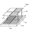
- FIG. 2 is a schematic diagram showing a schematic configuration of the imaging device according to the embodiment.
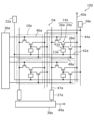
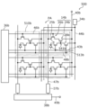
- FIG. 3A is a schematic diagram showing an exemplary circuit configuration of a pixel including a first photoelectric conversion unit and peripheral circuits in the imaging device according to the embodiment;
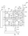
- FIG. 3B is a schematic diagram showing an exemplary circuit configuration of a pixel including a second photoelectric conversion unit and peripheral circuits in the imaging device according to the embodiment;
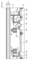
- FIG. 4 is a cross-sectional view schematically showing an exemplary cross-sectional structure of a pixel in the imaging device according to the embodiment.
- FIG. 5 is a schematic diagram showing the configuration of another imaging device according to the embodiment.
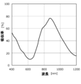
- FIG. 6 is a diagram showing an example of an absorption spectrum in a photoelectric conversion layer containing tin naphthalocyanine.
- 7A is a cross-sectional view schematically showing an example of a configuration of a photoelectric conversion layer in a first photoelectric conversion unit according to the embodiment
- FIG. 7B is a cross-sectional view schematically showing an example of a configuration of a photoelectric conversion layer in a second photoelectric conversion section according to the embodiment
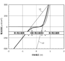
- FIG. FIG. 8 is a graph showing exemplary photocurrent characteristics of the photoelectric conversion layer according to the embodiment.
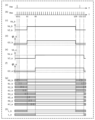
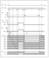
- FIG. 9 is a diagram for explaining an operation example of the imaging device according to the embodiment
- FIG. 10 is a diagram for explaining a comparative example of the operation of the imaging device.
- FIG. 9 is a diagram for explaining an operation example of the imaging device according to the embodiment
- FIG. 10 is a diagram for explaining a comparative example of the operation of the imaging device.
- FIG. 11 is a schematic diagram showing a schematic configuration of an imaging device according to Modification 1.
- FIG. 12 is a schematic diagram showing an exemplary circuit configuration of a pixel including a second photoelectric conversion unit and peripheral circuits in an imaging device according to Modification 2.
- FIG. 13 is a cross-sectional view schematically showing an exemplary cross-sectional structure of a pixel in an imaging device according to modification 2.
- FIG. 14A and 14B are diagrams for explaining an operation example of the imaging device according to Modification 2.
- the plurality of photoelectric conversion units include a photoelectric conversion unit having sensitivity in the invisible wavelength region, so that an image of invisible light can be acquired.
- Invisible light images may be able to obtain information that cannot be confirmed with visible light, and are useful for crime prevention, inspection, and the like.
- the amount of ambient light may be insufficient. done.
- the invisible illumination light also enters the photoelectric conversion units that are not used for imaging the invisible illumination light among the plurality of photoelectric conversion units.
- the imaging device includes a photoelectric conversion unit having sensitivity in the near-infrared wavelength region and a photoelectric conversion unit having sensitivity in the visible light wavelength region
- the near-infrared illumination light is a photoelectric conversion unit having sensitivity in the visible light wavelength region. It also enters the conversion section. Since near-infrared illumination light often has visible light wavelength components such as red in part, the near-infrared illumination light causes the photoelectric conversion of the photoelectric conversion unit that is sensitive to the visible light wavelength region. occurs. As a result, the amount of signal charge generated by the photoelectric conversion unit having sensitivity in the visible light wavelength region changes, and the image quality of the resulting image deteriorates, such as color shift.
- the present disclosure has been made based on such knowledge, and can suppress image quality deterioration due to invisible illumination light in an imaging device having a plurality of photoelectric conversion units including a photoelectric conversion unit having sensitivity in an invisible wavelength range.
- An imaging device and camera system are provided. Details are described below.
- An imaging device includes first pixels and second pixels.
- the first pixel generates a signal charge by photoelectric conversion and has sensitivity in a first invisible wavelength region; a first signal detection circuit connected to the first photoelectric conversion unit; including.
- the second pixel includes a second photoelectric conversion section that generates a signal charge by photoelectric conversion and has sensitivity in a second wavelength band, and a second signal detection circuit connected to the second photoelectric conversion section.
- the exposure period of the second photoelectric conversion unit is the light from the illumination that is incident on the first photoelectric conversion unit and does not overlap with the light emission period of the light having the emission peak in the first wavelength band.
- unintended photoelectric conversion tends to occur in the second photoelectric conversion unit due to light having an emission peak in the first wavelength band for imaging using the first photoelectric conversion unit. Since the exposure period of the second photoelectric conversion unit does not overlap with the light emission period of light having an emission peak in the first wavelength band, even if the light has a component that affects the photoelectric conversion of the second photoelectric conversion unit. , the light does not generate unintended signal charges in the second photoelectric conversion unit. Therefore, image quality deterioration can be suppressed.
- the imaging device according to the second aspect of the present disclosure may be the imaging device according to the first aspect, and the first pixel and the second pixel may each be an effective pixel.
- an imaging device is the imaging device according to the first aspect or the second aspect, in which the first photoelectric conversion section and the second photoelectric conversion section are stacked. good too.
- an imaging device may be the imaging device according to any one of the first aspect to the third aspect, and may further include at least one voltage supply circuit,
- Each of the first photoelectric conversion unit and the second photoelectric conversion unit includes a pixel electrode, a counter electrode facing the pixel electrode, and a photoelectric conversion layer positioned between the pixel electrode and the counter electrode.
- the sensitivity of at least one of the first photoelectric conversion unit and the second photoelectric conversion unit can be changed by changing the voltage applied between the pixel electrode and the counter electrode by the at least one voltage supply circuit. It may be variable.
- the sensitivity at the time of imaging using at least one of the first photoelectric conversion unit and the second photoelectric conversion unit can be adjusted only by changing the applied voltage.
- an imaging device is the imaging device according to the fourth aspect, wherein the at least one of the first photoelectric conversion unit and the second photoelectric conversion unit is the at least It may be driven by a global shutter method in which an exposure period is defined by changing the voltage applied between the pixel electrode and the counter electrode by one voltage supply circuit.
- the imaging device is the imaging device according to the fourth aspect, in which each of the first photoelectric conversion unit and the second photoelectric conversion unit supplies the at least one voltage It may be driven by a global shutter method in which the exposure period is defined by the change in the voltage applied between the pixel electrode and the counter electrode by the circuit.
- an imaging device is an imaging device according to any one of the first to sixth aspects, wherein the third photoelectric conversion unit and the third photoelectric conversion unit and a connected third signal detection circuit.
- each photoelectric conversion unit has sensitivity in the wavelength regions of red, green, and blue, color images can be easily obtained.
- the imaging device further includes a fourth photoelectric conversion unit, if each photoelectric conversion unit has sensitivity in the wavelength regions of red, green, blue, and near-infrared rays, a color image and a near-infrared image can be easily obtained. can be obtained.
- an imaging device is the imaging device according to any one of the first aspect to the seventh aspect, wherein the first wavelength range is a wavelength in the near-infrared wavelength range and the second wavelength range may be a wavelength range within the visible light wavelength range.
- a visible light image and a near-infrared image can be acquired with one imaging device.
- an imaging device is the imaging device according to the eighth aspect, wherein the exposure period of the first photoelectric conversion unit is longer than the exposure period of the second photoelectric conversion unit. It can be short.
- a photoelectric conversion part having sensitivity in the near-infrared wavelength region is likely to generate dark current due to thermal excitation because the bandgap of the photoelectric conversion material used is narrow.
- an imaging device is the imaging device according to any one of the first to seventh aspects, wherein the first wavelength range is a wavelength range within an ultraviolet wavelength range and the second wavelength range may be a wavelength range within a visible light wavelength range.
- a visible light image and an ultraviolet image can be acquired with one imaging device.
- an imaging device is the imaging device according to any one of the first to seventh aspects, wherein the first wavelength range and the second wavelength range are each: The wavelength range may be in the near-infrared wavelength range.
- images corresponding to near-infrared rays with different wavelengths can be acquired with a single imaging device.
- an imaging device is the imaging device according to any one of the first to eleventh aspects, wherein the second photoelectric conversion unit includes a silicon photodiode.
- a camera system includes an imaging device according to any one of the first to twelfth aspects, and an illumination device that emits light having an emission peak in the first wavelength range.
- the illumination device does not emit the light during the exposure period of the second photoelectric conversion unit.
- the light emitted by the lighting device during the exposure period of the second photoelectric conversion unit does not enter the second photoelectric conversion unit, so that the light does not generate unintended signal charges in the second photoelectric conversion unit. Therefore, light having an emission peak in the first wavelength band does not affect the output of an image captured using the second photoelectric conversion unit, and image quality deterioration can be suppressed.
- the camera system according to the fourteenth aspect of the present disclosure is the camera system according to the thirteenth aspect, wherein the illumination device emits the light during a period overlapping with the exposure period of the first photoelectric conversion unit. good too.
- the light emitted by the lighting device can be captured using the first photoelectric conversion unit, so the image quality of the captured image can be improved.
- the terms “upper” and “lower” do not refer to the upward direction (vertically upward) and the downward direction (vertically downward) in absolute spatial recognition, but are based on the stacking order in the stacking structure. It is used as a term defined by a relative positional relationship. Specifically, the light-receiving side of the imaging device is defined as “upper”, and the side opposite to the light-receiving side is defined as “lower”. Note that terms such as “upper” and “lower” are used only to specify the mutual arrangement of members, and are not intended to limit the orientation of the imaging apparatus when it is used.
- the terms “above” and “below” are used not only when two components are spaced apart from each other and there is another component between the two components, but also when two components are spaced apart from each other. It also applies when two components are in contact with each other and are placed in close contact with each other.
- FIG. 1 is a block diagram showing an example of the functional configuration of the camera system according to this embodiment.
- the camera system 1 includes an imaging device 100, an illumination device 200, and a control section 300.
- illumination light 602 emitted by the illumination device 200 is reflected by the subject 600 .
- the reflected light 604 generated by the reflection of the illumination light 602 by the subject 600 is converted into electric charge by the photoelectric conversion unit of the imaging device 100, and is extracted as an electric signal to be imaged.
- imaging device 100, lighting device 200, and control unit 300 are shown as separate functional blocks, but imaging device 100, lighting device 200, and control unit 300 Two or more may be integrated.
- imaging device 100 may include lighting device 200 .
- the imaging device 100 converts light incident on the camera system 1 into an electrical signal and outputs an image (image signal).
- the imaging device 100 includes a first photoelectric conversion unit 13a and a second photoelectric conversion unit 13b.
- Each of the first photoelectric conversion unit 13a and the second photoelectric conversion unit 13b is, for example, a photoelectric conversion element.
- Light from illumination for example, enters the first photoelectric conversion unit 13a and the second photoelectric conversion unit 13b.
- the illumination light incident on the first photoelectric conversion unit 13a and the second photoelectric conversion unit 13b is mainly reflected light generated by reflection of the illumination light emitted by the illumination device 200 on the subject. is.
- the first photoelectric conversion unit 13a and the second photoelectric conversion unit 13b each generate signal charges through photoelectric conversion.
- a signal corresponding to the amount of signal charge generated by each of the first photoelectric conversion unit 13a and the second photoelectric conversion unit 13b is read out and output from the imaging device 100 as an image signal.
- the first photoelectric conversion unit 13a and the second photoelectric conversion unit 13b have sensitivities in different wavelength ranges.
- the first photoelectric conversion unit 13a has sensitivity to the invisible first wavelength band.
- the second photoelectric conversion unit 13b has sensitivity in the second wavelength band.
- having sensitivity to a certain wavelength means having an external quantum efficiency of 1% or more at a certain wavelength.
- the illumination device 200 irradiates the subject with illumination light.
- the illumination device 200 emits, as illumination light, at least light having an emission peak in the first wavelength region to which the first photoelectric conversion unit 13a is sensitive.
- the illumination device 200 has, for example, a first light source 210a and a second light source 210b.
- the first light source 210a emits light containing, for example, a component having a wavelength in at least part of the first wavelength band to which the first photoelectric conversion section 13a is sensitive.
- the first light source 210a emits light having an emission peak in, for example, the first wavelength band.
- the second light source 210b emits light containing, for example, a component having a wavelength in at least part of the second wavelength range to which the second photoelectric conversion section 13b is sensitive.
- the second light source 210b emits light having an emission peak in the second wavelength band, for example.
- the types of light sources used as the first light source 210a and the second light source 210b are not particularly limited as long as they can emit light of desired wavelengths.
- the first light source 210a and the second light source 210b are, for example, halogen light sources, LED (Light Emitting Diode) light sources, organic EL (Electro Luminescence) light sources, laser diode light sources, or the like.
- a plurality of light sources having different emission wavelengths may be used in combination for the first light source 210a and the second light source 210b.
- the first wavelength range is an invisible wavelength range as described above, and is, for example, a wavelength range included in the ultraviolet wavelength range or the near-infrared wavelength range. Therefore, it is possible to capture an image using invisible light such as ultraviolet light or near-infrared light using the first photoelectric conversion unit 13a, so that an image useful for crime prevention or inspection can be acquired.
- the second wavelength range is, for example, a wavelength range included in any one of the ultraviolet wavelength range, the visible light wavelength range, and the near-infrared wavelength range.
- the first photoelectric conversion unit 13a may have sensitivity to wavelengths other than the first wavelength range.
- the second photoelectric conversion unit 13b may have sensitivity to wavelengths other than the second wavelength range.
- the first wavelength range is a wavelength range within the near-infrared wavelength range
- the second wavelength range is a wavelength range within the visible light wavelength range. Therefore, the first light source 210a emits light having an emission peak in the near-infrared wavelength region. Also, the second light source 210b emits light having an emission peak in the visible light wavelength region. In this case, the light emitted by the first light source 210a is converted by the first photoelectric converter 13a having sensitivity in the near-infrared wavelength region, extracted as an electric signal, and captured. Also, the light emitted by the second light source 210b is converted by the second photoelectric conversion unit 13b having sensitivity in the visible light wavelength region, extracted as an electric signal, and captured. This makes it possible to realize the imaging device 100 that separates and extracts signals corresponding to visible light and near-infrared light. Therefore, for example, a visible light image and a near-infrared image can be acquired.
- the near-infrared wavelength region refers to, for example, a wavelength region of 680 nm or more and 3000 nm or less.
- the near-infrared wavelength region may refer to a wavelength region of 700 nm or more and 2000 nm or less, or may refer to a wavelength region of 700 nm or more and 1600 nm or less.
- the visible light wavelength region refers to, for example, a wavelength region of 380 nm or more and less than 680 nm.
- the ultraviolet wavelength range refers to, for example, a wavelength range of 100 nm or more and less than 380 nm, and may refer to a wavelength range of 200 nm or more and less than 380 nm.
- all electromagnetic waves including visible light, infrared rays and ultraviolet rays are expressed as "light" for convenience.
- the first wavelength range may be a wavelength range within the ultraviolet wavelength range
- the second wavelength range may be a wavelength range within the visible light wavelength range. Accordingly, the imaging device 100 that separates and extracts signals corresponding to visible light and ultraviolet light can be realized. Therefore, for example, a visible light image and an ultraviolet image can be acquired.
- each of the first wavelength band and the second wavelength band may be a wavelength band within the near-infrared wavelength region. Accordingly, the imaging apparatus 100 that separates and extracts signals corresponding to near-infrared rays having different wavelengths can be realized. Therefore, for example, two types of near-infrared images with different wavelengths can be acquired. For example, by generating a difference image using such two types of near-infrared images, it is possible to obtain a near-infrared image in which the influence of absorption of ambient light or moisture is reduced.
- At least one of the first wavelength range and the second wavelength range is a wavelength range within the near-infrared wavelength range
- at least one may be a wavelength range within the range of 820 nm or more and 980 nm or less.
- an inexpensive LED light source having an emission peak at 820 nm or more and 980 nm or less can be used as the light source of the illumination device 200 that emits illumination light.
- the number of light sources included in the lighting device 200 is not limited to two, and may be one, or three or more.
- lighting device 200 may be configured to include only first light source 210a as a light source.
- the second photoelectric conversion unit 13b converts reflected light, which is ambient light or light from an external light source reflected by the object, into electric charges.
- the first light source 210a and the second light source 210b may not be provided in one lighting device, and the camera system 1 includes the lighting device having the first light source 210a and the lighting device having the second light source 210b. and a plurality of lighting devices may be provided.
- the camera system 1 may not include the illumination device 200 .
- the control unit 300 is a control circuit that controls operations of the imaging device 100 and the lighting device 200 .
- the control unit 300 outputs various drive signals to the imaging device 100 and the lighting device 200, for example.
- Control unit 300 is realized by, for example, a microcomputer.
- the functions of the control unit 300 may be realized by a combination of a general-purpose processing circuit and software, or may be realized by hardware specialized for such processing.
- control unit 300 for example, the function of controlling the driving of the imaging device 100 may be included in the imaging device 100 .
- the control unit 300 may be provided in the imaging device 100 as a control circuit or the like. Therefore, the driving of the peripheral circuits and pixels of the imaging device 100 to be described later may be performed based on the control of the control unit 300 provided outside the imaging device 100 . It may be performed based on the control of the unit 300).
- FIG. 2 is a schematic diagram showing a schematic configuration of an imaging device according to this embodiment.
- FIG. 2 schematically shows a photoelectric conversion unit of each pixel of the imaging device 100 according to the present embodiment and a signal detection circuit connected thereto.
- the imaging device 100 includes a first photoelectric conversion unit 13a, a signal detection circuit 14a connected to the first photoelectric conversion unit 13a, a second photoelectric conversion unit 13b, and a second photoelectric conversion unit. 13b, and a semiconductor substrate 20 provided with the signal detection circuit 14a and the signal detection circuit 14b.
- the signal detection circuit 14a is an example of a first signal detection circuit.
- the signal detection circuit 14b is an example of a second signal detection circuit.
- FIG. 2 shows the first photoelectric conversion unit 13a and the second photoelectric conversion unit 13b for four pixels, respectively. is not particularly limited. Also, the number of pixels in the first photoelectric conversion unit 13a and the number of pixels in the second photoelectric conversion unit 13b may be the same or different. For example, FIG. 2 illustrates an example in which a four-pixel second photoelectric conversion unit 13b is stacked on a four-pixel first photoelectric conversion unit 13a. 4 pixels of the second photoelectric conversion unit 13b may be stacked.
- Both the first photoelectric conversion unit 13a and the second photoelectric conversion unit 13b may have sensitivity to at least one of visible light, near-infrared rays, infrared rays, and ultraviolet rays.
- a color filter in a Bayer array is provided above the second photoelectric conversion unit 13b having sensitivity in the entire visible light wavelength region, and each pixel provided in the second photoelectric conversion unit 13b is connected to the corresponding color filter. Accordingly, pixel signals corresponding to red, blue and green light intensities may be output.
- each pixel provided in the first photoelectric conversion unit 13a having sensitivity in the near-infrared wavelength region may output a pixel signal corresponding to the intensity of near-infrared rays. Thereby, a color image corresponding to the signal charge of the second photoelectric conversion unit 13b is obtained, and a near-infrared image corresponding to the signal charge of the first photoelectric conversion unit 13a is obtained.
- the signal detection circuit 14a and the signal detection circuit 14b are formed on the same plane on the semiconductor substrate 20 in the example shown in FIG.
- the signal detection circuits 14a and 14b may be formed side by side on the same plane on the semiconductor substrate 20 as shown in FIG. 2, or may be vertically divided and formed on different planes.
- FIG. 3A is a schematic diagram showing an exemplary circuit configuration of a pixel including a first photoelectric conversion unit and peripheral circuits in the imaging device according to the present embodiment.
- FIG. 3B is a schematic diagram showing an exemplary circuit configuration of a pixel including a second photoelectric conversion unit and peripheral circuits in the imaging device according to the present embodiment.
- the imaging device 100 includes a plurality of pixels including a plurality of pixels 10a and a plurality of pixels 10b, and peripheral circuits. More specifically, the imaging device 100 includes a pixel array PA including a plurality of two-dimensionally arranged pixels 10a and a plurality of two-dimensionally arranged pixels 10b, and a peripheral circuit.
- 3A and 3B schematically show examples in which the pixels 10a and the pixels 10b are arranged in a matrix of two rows and two columns, respectively.
- the first photoelectric conversion unit 13a and the signal detection circuit 14a constitute at least part of the pixel 10a
- the second photoelectric conversion unit 13b and the signal detection circuit 14b constitute at least part of the pixel 10b.
- the first photoelectric conversion unit 13a of the pixel 10a and the second photoelectric conversion unit 13b of the pixel 10b are stacked.
- the number and arrangement of pixels 10a and pixels 10b in imaging device 100 are not limited to the examples shown in FIGS. 3A and 3B.
- the pixel 10a is an example of a first pixel
- the pixel 10b is an example of a second pixel.
- the peripheral circuit drives the pixel array PA and acquires an image based on signal charges generated by the first photoelectric conversion unit 13a and the second photoelectric conversion unit 13b.
- the peripheral circuits include, for example, a voltage supply circuit 32a connected to the pixels 10a, a reset voltage source 34a, a vertical scanning circuit 36a, a column signal processing circuit 37a, a horizontal signal readout circuit 38a, and a voltage source connected to the power line 40a.
- the peripheral circuits include, for example, a voltage supply circuit 32b connected to the pixel 10b, a reset voltage source 34b, a vertical scanning circuit 36b, a column signal processing circuit 37b, a horizontal signal readout circuit 38b, and a voltage source connected to the power supply line 40b.
- the imaging apparatus 100 may include a control circuit that controls driving of peripheral circuits other than itself as a circuit included in the peripheral circuits.
- the pixels 10a and 10b are, for example, effective pixels.
- effective pixels are pixels that are actually used for image output or pixels that are used during sensing, and do not include optical black pixels and dummy pixels that are used to measure dark noise.
- the pixel 10a shown in FIG. 3A and the peripheral circuit connected to the pixel 10a and the pixel 10b shown in FIG. 3B and the peripheral circuit connected to the pixel 10b have, for example, functionally similar circuit configurations.
- a circuit configuration of the pixel 10a having the first photoelectric conversion unit 13a and the pixel 10b having the second photoelectric conversion unit 13b will be described with reference to FIGS. 3A and 3B.
- Each pixel 10a has a first photoelectric conversion unit 13a and a signal detection circuit 14a.
- Each pixel 10b has a second photoelectric conversion unit 13b and a signal detection circuit 14b.
- each of the first photoelectric conversion unit 13a and the second photoelectric conversion unit 13b has a photoelectric conversion layer sandwiched between two electrodes facing each other, and converts incident light into receive and generate signal charges.
- the entire first photoelectric conversion unit 13a does not need to be an independent element for each pixel 10a.
- a portion of the first photoelectric conversion unit 13a may extend over a plurality of pixels 10a.
- the second photoelectric conversion unit 13b does not need to be an independent element for each pixel 10b as a whole.
- the signal detection circuit 14a is a circuit that detects signal charges generated by the first photoelectric conversion unit 13a.
- the signal detection circuit 14b is a circuit that detects signal charges generated by the second photoelectric conversion unit 13b.
- the signal detection circuit 14a includes a signal detection transistor 24a and an address transistor 26a.
- the signal detection circuit 14b also includes a signal detection transistor 24b and an address transistor 26b.
- Signal detection transistors 24a and 24b and address transistors 26a and 26b are, for example, field effect transistors (FETs), respectively, where N-channel MOSFETs (Metal Oxide Semiconductor Field Effect Transistor).
- Each transistor such as signal detection transistors 24a and 24b, address transistors 26a and 26b, and reset transistors 28a and 28b to be described later, has a control terminal, an input terminal and an output terminal.
- a control terminal is, for example, a gate.
- the input terminal is one of the drain and the source, for example the drain.
- the output terminal is the other of the drain and the source, for example the source.
- the control terminal of the signal detection transistor 24a has an electrical connection with the first photoelectric conversion section 13a.
- the signal charge generated by the first photoelectric conversion unit 13a is accumulated in a region including the charge accumulation node 41a between the gate of the signal detection transistor 24a and the first photoelectric conversion unit 13a.
- the control terminal of the signal detection transistor 24b is electrically connected to the second photoelectric conversion section 13b.
- the signal charges generated by the second photoelectric conversion unit 13b are accumulated in a region including the charge accumulation node 41b between the gate of the signal detection transistor 24b and the second photoelectric conversion unit 13b.
- the signal charges are holes or electrons.
- a charge storage node is at least part of a charge storage region that stores signal charge, and is also called a “floating diffusion node”. The details of the structures of the first photoelectric conversion unit 13a and the second photoelectric conversion unit 13b will be described later.
- the first photoelectric conversion unit 13a of each pixel 10a further has a connection with the sensitivity control line 42a.
- the sensitivity control line 42a is connected to the voltage supply circuit 32a.
- the second photoelectric conversion unit 13b of each pixel 10b is further connected to a sensitivity control line 42b.
- the sensitivity control line 42b is connected to the voltage supply circuit 32b.
- the voltage supply circuit is also called a sensitivity control electrode supply circuit.
- Each of the voltage supply circuits 32a and 32b is a circuit capable of supplying at least two voltages.
- the voltage supply circuit 32a supplies voltage to the first photoelectric conversion unit 13a. Specifically, the voltage supply circuit 32a supplies a predetermined voltage to the first photoelectric conversion unit 13a through the sensitivity control line 42a when the imaging device 100 operates. Also, the voltage supply circuit 32b supplies voltage to the second photoelectric conversion unit 13b. Specifically, the voltage supply circuit 32b supplies a predetermined voltage to the second photoelectric conversion section 13b through the sensitivity control line 42b when the imaging device 100 operates.
- the voltage supply circuits 32a and 32b are not limited to a specific power supply circuit, and may be a circuit that generates a predetermined voltage, or a circuit that converts a voltage supplied from another power source into a predetermined voltage. good too.
- the voltage supplied from the voltage supply circuit 32a to the first photoelectric conversion unit 13a is switched between a plurality of voltages different from each other, whereby the charge storage node 41a from the first photoelectric conversion unit 13a is controlled to start and end the accumulation of signal charges in the .
- the voltage supplied from the voltage supply circuit 32b to the second photoelectric conversion unit 13b is switched between a plurality of voltages different from each other. Start and end of accumulation is controlled.
- the electronic shutter is switched. Action is performed. An example of the operation of the imaging device 100 will be described later.
- Each pixel 10a is connected to a power supply line 40a that supplies power supply voltage VDD.
- Each pixel 10b has a connection with a power supply line 40b that supplies a power supply voltage VDD.
- the input terminal of the signal detection transistor 24a is connected to the power line 40a. Since the power line 40a functions as a source follower power supply, the signal detection transistor 24a amplifies and outputs the signal generated by the first photoelectric conversion section 13a.
- the input terminal of the signal detection transistor 24b is connected to the power line 40b. Since the power line 40b functions as a source follower power supply, the signal detection transistor 24b amplifies and outputs the signal generated by the second photoelectric conversion section 13b.
- the input terminal of the address transistor 26a is connected to the output terminal of the signal detection transistor 24a.
- the output terminal of the address transistor 26a is connected to one of a plurality of vertical signal lines 47a arranged for each column of pixels 10a in the pixel array PA.
- the control terminal of the address transistor 26a is connected to the address control line 46a, and by controlling the potential of the address control line 46a, the output of the signal detection transistor 24a can be selectively read out to the corresponding vertical signal line 47a. can be done.
- the input terminal of the address transistor 26b is connected to the output terminal of the signal detection transistor 24b.
- the output terminal of the address transistor 26b is connected to one of a plurality of vertical signal lines 47b arranged for each column of pixels 10b in the pixel array PA.
- the control terminal of the address transistor 26b is connected to the address control line 46b, and by controlling the potential of the address control line 46b, the output of the signal detection transistor 24b can be selectively read out to the corresponding vertical signal line 47b. can be done.
- the address control line 46a is connected to the vertical scanning circuit 36a. Also, in the example shown in FIG. 3B, the address control line 46b is connected to the vertical scanning circuit 36b.
- the vertical scanning circuit is also called "row scanning circuit".
- the vertical scanning circuit 36a selects a plurality of pixels 10a arranged in each row by applying a predetermined voltage to the address control line 46a.
- the vertical scanning circuit 36b applies a predetermined voltage to the address control line 46b to select the plurality of pixels 10b arranged in each row on a row-by-row basis.
- the vertical signal line 47a is a main signal line that transmits pixel signals from the plurality of pixels 10a of the pixel array PA to peripheral circuits.
- a column signal processing circuit 37a is connected to the vertical signal line 47a.
- the vertical signal line 47b is a main signal line that transmits pixel signals from the plurality of pixels 10b of the pixel array PA to peripheral circuits.
- a column signal processing circuit 37b is connected to the vertical signal line 47b.
- the column signal processing circuit is also called "row signal storage circuit”.
- the column signal processing circuits 37a and 37b respectively perform noise suppression signal processing typified by correlated double sampling, analog-to-digital conversion (AD conversion), and the like. As shown in FIG.
- a column signal processing circuit 37a is provided corresponding to each column of pixels 10a in the pixel array PA.
- a horizontal signal readout circuit 38a is connected to these column signal processing circuits 37a.
- the column signal processing circuit 37b is provided corresponding to each column of the pixels 10b in the pixel array PA.
- a horizontal signal readout circuit 38b is connected to these column signal processing circuits 37b.
- the horizontal signal readout circuit is also called a "column scanning circuit".
- the horizontal signal readout circuit 38a sequentially reads signals from the plurality of column signal processing circuits 37a to the horizontal common signal line 49a. Further, the horizontal signal readout circuit 38b sequentially reads signals from the plurality of column signal processing circuits 37b to the horizontal common signal line 49b.
- the pixel 10a has a reset transistor 28a.
- the pixel 10b has a reset transistor 28b.
- Reset transistors 28a and 28b can be, for example, field effect transistors, as can signal detection transistors 24a and 24b and address transistors 26a and 26b, respectively.
- N-channel MOSFETs are used as the reset transistors 28a and 28b will be described below unless otherwise specified.
- the reset transistor 28a is connected between the reset voltage line 44a that supplies the reset voltage Vr and the charge storage node 41a.
- a control terminal of the reset transistor 28a is connected to a reset control line 48a, and the potential of the charge storage node 41a can be reset to the reset voltage Vr by controlling the potential of the reset control line 48a.
- the reset control line 48a is connected to the vertical scanning circuit 36a. Therefore, when the vertical scanning circuit 36a applies a predetermined voltage to the reset control line 48a, the plurality of pixels 10a arranged in each row can be reset row by row.
- reset transistor 28b is connected between reset voltage line 44b that supplies reset voltage Vr and charge storage node 41b.
- a control terminal of the reset transistor 28b is connected to a reset control line 48b, and the potential of the charge storage node 41b can be reset to the reset voltage Vr by controlling the potential of the reset control line 48b.
- the reset control line 48b is connected to the vertical scanning circuit 36b. Therefore, when the vertical scanning circuit 36b applies a predetermined voltage to the reset control line 48b, it is possible to reset the plurality of pixels 10b arranged in each row on a row-by-row basis.
- a reset voltage line 44a that supplies a reset voltage Vr to the reset transistor 28a is connected to the reset voltage source 34a.
- a reset voltage line 44b for supplying a reset voltage Vr to the reset transistor 28b is connected to the reset voltage source 34b.
- a reset voltage source is also called a "reset voltage supply circuit".
- the reset voltage sources 34a and 34b only need to have a configuration capable of supplying a predetermined reset voltage Vr to the reset voltage lines 44a and 44b during operation of the imaging device 100, similarly to the voltage supply circuits 32a and 32b described above. , is not limited to any particular power supply circuit.
- Each of voltage supply circuits 32a and 32b and reset voltage sources 34a and 34b may be part of a single voltage supply circuit or may be independent and separate voltage supply circuits.
- One or both of the voltage supply circuit 32a and the reset voltage source 34a may be part of the vertical scanning circuit 36a.
- the sensitivity control voltage from the voltage supply circuit 32a and/or the reset voltage Vr from the reset voltage source 34a may be supplied to each pixel 10a via the vertical scanning circuit 36a.
- one or both of the voltage supply circuit 32b and the reset voltage source 34b may be part of the vertical scanning circuit 36b.
- the sensitivity control voltage from the voltage supply circuit 32b and/or the reset voltage Vr from the reset voltage source 34b may be supplied to each pixel 10b via the vertical scanning circuit 36b.
- the power supply voltage VDD of the signal detection circuits 14a and 14b can be used as the reset voltage Vr.
- a voltage supply circuit (not shown in FIG. 3A) that supplies a power supply voltage to each pixel 10a and the reset voltage source 34a can be shared.
- the power supply line 40a and the reset voltage line 44a can be shared, the wiring in the pixel array PA can be simplified.
- a voltage supply circuit (not shown in FIG. 3B) that supplies a power supply voltage to each pixel 10b and the reset voltage source 34b can be shared.
- the power supply line 40b and the reset voltage line 44b can be shared, the wiring in the pixel array PA can be simplified.
- using different voltages for the reset voltage Vr and the power supply voltage VDD of the signal detection circuits 14a and 14b enables more flexible control of the imaging device 100.
- FIG. 4 is a cross-sectional view schematically showing an exemplary cross-sectional structure of pixels 10a and 10b according to the present embodiment.
- the above-described signal detection transistors 24a and 24b, address transistors 26a and 26b and reset transistors 28a and 28b are formed on semiconductor substrate 20.
- the semiconductor substrate 20 is not limited to a substrate whose entirety is a semiconductor.
- the semiconductor substrate 20 may be an insulating substrate or the like having a semiconductor layer provided on the surface on which the photosensitive region is formed.
- the semiconductor substrate 20 has a plurality of semiconductor layers, and the signal detection transistor 24a, the address transistor 26a and the reset transistor 28a and the signal detection transistor 24b, the address transistor 26b and the reset transistor 28b are formed in different semiconductor layers.
- the signal detection transistor 24a, the address transistor 26a and the reset transistor 28a and the signal detection transistor 24b, the address transistor 26b and the reset transistor 28b are formed in different semiconductor layers.
- Si P-type silicon
- FIG. 4 an example in which the first photoelectric conversion section 13a and the second photoelectric conversion section 13b having the same size are arranged in the same region of the semiconductor substrate 20 in plan view will be described.
- the semiconductor substrate 20 has impurity regions 26s, 24s, 24d, 28d and 28s, and an isolation region 20t for electrical isolation between pixels.
- impurity regions 26s, 24s, 24d, 28d and 28s are N-type regions.
- the element isolation region 20t is also provided between the impurity regions 24d and 28d.
- the element isolation region 20t is formed, for example, by implanting acceptor ions under predetermined implantation conditions.
- the impurity regions 26s, 24s, 24d, 28d and 28s are diffusion layers formed in the semiconductor substrate 20, for example.
- signal detection transistors 24a and 24b each include impurity regions 24s and 24d and a gate electrode 24g.
- Gate electrode 24g is formed using a conductive material.
- the conductive material is, for example, polysilicon imparted with conductivity by being doped with impurities, but may also be a metal material.
- the impurity region 24s functions as, for example, source regions of the signal detection transistors 24a and 24b.
- the impurity region 24d functions as, for example, drain regions of the signal detection transistors 24a and 24b. Channel regions of signal detection transistors 24a and 24b are formed between impurity regions 24s and 24d.
- the address transistors 26a and 26b each include impurity regions 26s and 24s and a gate electrode 26g connected to an address control line 46a or 46b (see FIGS. 3A and 3B) not shown in FIG.
- Gate electrode 26g is formed using a conductive material.
- the conductive material is, for example, polysilicon imparted with conductivity by being doped with impurities, but may also be a metal material.
- signal detection transistor 24a and address transistor 26a are electrically connected to each other by sharing impurity region 24s.
- signal detection transistor 24b and address transistor 26b are electrically connected to each other by sharing impurity region 24s.
- Impurity region 26s functions as, for example, source regions of address transistors 26a and 26b.
- Impurity region 26s is connected to vertical signal line 47a or 47b (see FIGS. 3A and 3B) not shown in FIG.
- the reset transistors 28a and 28b respectively include impurity regions 28d and 28s and a gate electrode 28g connected to a reset control line 48a or 48b (see FIGS. 3A and 3B) not shown in FIG.
- the gate electrode 28g is formed using, for example, a conductive material.
- the conductive material is, for example, polysilicon imparted with conductivity by being doped with impurities, but may also be a metal material.
- the impurity region 28s functions as, for example, source regions of the reset transistors 28a and 28b.
- Impurity region 28s is connected to reset voltage line 44a or 44b (see FIGS. 3A and 3B) not shown in FIG.
- Impurity region 28d functions as, for example, a drain region of reset transistors 28a and 28b.
- An interlayer insulating layer 50 is arranged on the semiconductor substrate 20 so as to cover the signal detection transistors 24a and 24b, the address transistors 26a and 26b, and the reset transistors 28a and 28b.
- the interlayer insulating layer 50 is made of, for example, an insulating material such as silicon oxide.
- wiring layers 56 a and 56 b may be arranged in the interlayer insulating layer 50 .
- the wiring layers 56a and 56b are made of metal such as copper, for example.
- the wiring layer 56a may include wiring such as the above vertical signal line 47a in part thereof, for example.
- the wiring layer 56b may include wiring such as the above vertical signal line 47b in part thereof, for example.
- the number of insulating layers in interlayer insulating layer 50 and the number of layers included in wiring layers 56a and 56b arranged in interlayer insulating layer 50 can be set arbitrarily, and are not limited to the example shown in FIG. .
- the first photoelectric conversion section 13a and the second photoelectric conversion section 13b are arranged on the interlayer insulating layer 50.
- the plurality of pixels 10a and the plurality of pixels 10b that constitute the pixel array PA are formed in and on the semiconductor substrate 20.
- a plurality of pixels 10a and pixels 10b arranged two-dimensionally on the semiconductor substrate 20 form a photosensitive region.
- the photosensitive area is also called the "pixel area”.
- the distance between two adjacent pixels 10a and the distance between two adjacent pixels 10b can each be approximately 2 ⁇ m, for example.
- the distance between two adjacent pixels is also called "pixel pitch”.
- the first photoelectric conversion unit 13a and the second photoelectric conversion unit 13b are supplied with light from above the first photoelectric conversion unit 13a and the second photoelectric conversion unit 13b, in other words, from the side opposite to the semiconductor substrate 20 side. Light enters from the side.
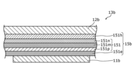
- the first photoelectric conversion section 13a includes a pixel electrode 11a, a counter electrode 12a, and a photoelectric conversion layer 15a arranged therebetween.
- the counter electrode 12a and the photoelectric conversion layer 15a are formed across a plurality of pixels 10a.
- the pixel electrode 11a is provided for each pixel 10a, and is electrically isolated from the pixel electrode 11a of the other pixel 10a by being spatially separated from the pixel electrode 11a of the other adjacent pixel 10a. ing.
- the second photoelectric conversion section 13b includes a pixel electrode 11b, a counter electrode 12b, and a photoelectric conversion layer 15b arranged therebetween.
- the counter electrode 12b and the photoelectric conversion layer 15b are formed across a plurality of pixels 10b.
- the pixel electrode 11b is provided for each pixel 10b, and is electrically separated from the pixel electrode 11b of the other pixel 10b by being spatially separated from the pixel electrode 11b of the other adjacent pixel 10b. ing.
- the second photoelectric conversion section 13b is stacked above the first photoelectric conversion section 13a with an insulating layer 62 interposed therebetween. Light transmitted through the second photoelectric conversion unit 13b and the insulating layer 62 is incident on the first photoelectric conversion unit 13a.
- the second photoelectric conversion unit 13b and the insulating layer 62 transmit at least part of the light of the wavelength to which the first photoelectric conversion unit 13a is sensitive. Thus, light incident on the first photoelectric conversion unit 13a passes through the second photoelectric conversion unit 13b.
- Light incident on the imaging device 100 enters both the first photoelectric conversion unit 13a and the second photoelectric conversion unit 13b. Therefore, even if light in a wavelength range to which one of the first photoelectric conversion unit 13a and the second photoelectric conversion unit 13b is sensitive is incident, the light may affect the photoelectric conversion of the other.
- a sealing layer, a color filter, a microlens, and the like may be further provided above the second photoelectric conversion unit 13b.
- the pixel electrode 11a is an electrode for reading out signal charges generated by the first photoelectric conversion unit 13a. At least one pixel electrode 11a exists for each pixel 10a. The pixel electrode 11a is electrically connected to the gate electrode 24g and the impurity region 28d of the signal detection transistor 24a. The pixel electrode 11b is an electrode for reading signal charges generated by the second photoelectric conversion unit 13b. At least one pixel electrode 11b exists for each pixel 10b. The pixel electrode 11b is electrically connected to the gate electrode 24g and the impurity region 28d of the signal detection transistor 24b. Also, the pixel electrode 11b is arranged on the first photoelectric conversion section 13a side of the photoelectric conversion layer 15b.
- the counter electrode 12a is arranged to face the pixel electrode 11a with the photoelectric conversion layer 15a interposed therebetween.
- the counter electrode 12a is arranged, for example, on the side of the photoelectric conversion layer 15a on which light is incident. Therefore, the light transmitted through the counter electrode 12a is incident on the photoelectric conversion layer 15a.
- the counter electrode 12a is arranged, for example, on the second photoelectric conversion section 13b side of the photoelectric conversion layer 15a. Therefore, the first photoelectric conversion section 13a and the second photoelectric conversion section 13b are stacked such that the counter electrode 12a faces the pixel electrode 11b.
- the counter electrode 12a and the pixel electrode 11b are adjacent to each other with the insulating layer 62 interposed therebetween.
- the counter electrode 12b is arranged to face the pixel electrode 11b with the photoelectric conversion layer 15b interposed therebetween.
- the counter electrode 12b is arranged, for example, on the side of the photoelectric conversion layer 15b on which light is incident. Therefore, the light transmitted through the counter electrode 12b is incident on the photoelectric conversion layer 15b.
- the pixel electrode 11b, the counter electrode 12a, and the counter electrode 12b are each transparent electrodes made of, for example, a transparent conductive material.
- Transparent as used herein means transmitting at least a portion of light in the wavelength range to be detected, and does not necessarily transmit light over the entire wavelength range of visible light.
- the counter electrode 12b transmits at least part of the light of the wavelength to which the first photoelectric conversion section 13a is sensitive and at least part of the light of the wavelength to which the second photoelectric conversion section 13b is sensitive.
- the pixel electrode 11b and the counter electrode 12a transmit at least part of the light of the wavelength to which the first photoelectric conversion unit 13a is sensitive.
- Transparent conducting oxides such as ITO, IZO, AZO, FTO, SnO 2 , TiO 2 and ZnO 2 can be used for the transparent electrode.
- the pixel electrode 11a is formed using a conductive material.
- the conductive material is, for example, a metal such as aluminum or copper, a metal nitride, or polysilicon that is doped with impurities to make it conductive.
- the pixel electrode 11a may be a light shielding electrode.
- a TaN electrode with a thickness of 100 nm as the pixel electrode 11a
- a sufficient light shielding property can be realized.
- channels of transistors in this example, at least one of the signal detection transistors 24a and 24b, the address transistors 26a and 26b, and the reset transistors 28a and 28b
- a light shielding film may be formed in the interlayer insulating layer 50 using the wiring layers 56a and 56b described above.
- the pixel electrode 11a may be a transparent electrode.
- the pixel electrode 11a and the counter electrode 12a may be arranged with their positions reversed from the arrangement shown in FIG. In this case, if the pixel electrode 11a is a transparent electrode and the counter electrode 12a is formed using a conductive material, it may not be a transparent electrode. Moreover, in this case, the plug 52a is arranged so as to penetrate the counter electrode 12a and the photoelectric conversion layer 15a.
- the pixel electrode 11b and the counter electrode 12b may be arranged with their positions reversed from the arrangement shown in FIG.
- the plug 52b is arranged so as to penetrate the counter electrode 12b and the photoelectric conversion layer 15b as well.
- first photoelectric conversion unit 13a and the second photoelectric conversion unit 13b may be arranged with their positions reversed from the arrangement shown in FIG.
- the photoelectric conversion layers 15a and 15b each receive incident light and generate hole-electron pairs.
- Photoelectric conversion layers 15a and 15b are each made of, for example, an organic material.
- each of the photoelectric conversion layers 15a and 15b may have a structure in which a plurality of layers are laminated. A specific example of the material forming the photoelectric conversion layers 15a and 15b will be described later.
- the counter electrode 12a has a connection with the sensitivity control line 42a connected to the voltage supply circuit 32a. Also, here, the counter electrode 12a is formed across a plurality of pixels 10a. Therefore, it is possible to collectively apply a desired magnitude of sensitivity control voltage from the voltage supply circuit 32a to the plurality of pixels 10a via the sensitivity control line 42a. Also, as described with reference to FIG. 3B, the counter electrode 12b has a connection with the sensitivity control line 42b connected to the voltage supply circuit 32b. Also, here, the counter electrode 12b is formed across a plurality of pixels 10b.
- At least one of the counter electrodes 12a and 12b may be provided separately for each pixel 10a or 10b as long as a desired sensitivity control voltage can be applied from the voltage supply circuit 32a or 32b.
- at least one of the photoelectric conversion layers 15a and 15b may be separately provided for each pixel 10a or 10b.
- the voltage supply circuits 32a and 32b respectively supply different voltages to the counter electrode 12a or 12b between the exposure period and the non-exposure period.
- the “exposure period” refers to accumulation of signal charge, which is one of positive and negative charges generated by photoelectric conversion of the first photoelectric conversion unit 13a and the second photoelectric conversion unit 13b, in a charge accumulation region or the like. , and may be called a "charge accumulation period”.
- non-exposure period a period other than the exposure period during which the imaging apparatus is in operation.
- the “non-exposure period” is not limited to the period during which light is blocked from entering the first photoelectric conversion unit 13a or the second photoelectric conversion unit 13b. A period during which light is applied to 13b may be included.
- the “non-exposure period” includes a period during which signal charges are unintentionally accumulated in the charge accumulation region due to the occurrence of parasitic sensitivity.
- the "non-exposure period” includes the “readout period” and the “reset period”.
- the “readout period” signals corresponding to the amount of signal charges generated by the first photoelectric conversion unit 13a and the second photoelectric conversion unit 13b (that is, the amount of signal charge accumulated in the charge accumulation region) are detected by signal detection circuits. 14a and 14b are readout periods.
- the “reset period” is a period for resetting the potential of the charge accumulation region that accumulates signal charges generated by the first photoelectric conversion unit 13a and the second photoelectric conversion unit 13b. Specifically, in the "reset period", the potential of the charge accumulation region is reset to the reset voltage Vr.
- an "exposure period”, a “non-exposure period”, a “readout period” and a “reset period” are defined for each of the pixels 10a and 10b.
- a signal corresponding to the amount of signal charge generated by the first photoelectric conversion unit 13a is read out. It can also be said that they are the “exposure period”, the “non-exposure period”, the “readout period” and the “reset period” of the first photoelectric conversion unit 13a.
- the "exposure period”, “non-exposure period”, “readout period” and “reset period” of the pixel 10b are set. can also be said to be the “exposure period”, the “non-exposure period”, the “readout period” and the “reset period” of the second photoelectric conversion unit 13b. Details of each period will be described later.
- one of the hole-electron pairs generated in the photoelectric conversion layer 15a by photoelectric conversion is used as a signal charge in the pixel. It can be collected by electrode 11a.
- holes can be selectively collected by the pixel electrode 11a by making the potential of the counter electrode 12a higher than that of the pixel electrode 11a.
- the potential of the counter electrode 12b with respect to the potential of the pixel electrode 11b, either holes or electrons of the hole-electron pairs generated in the photoelectric conversion layer 15b by photoelectric conversion are converted into signal charges. can be collected by the pixel electrode 11b as .
- holes can be selectively collected by the pixel electrode 11b by making the potential of the counter electrode 12b higher than that of the pixel electrode 11b.
- a case in which holes are used as signal charges will be exemplified below.
- electrons can also be used as signal charges.
- the potential of the counter electrode 12a is set lower than that of the pixel electrode 11a
- the potential of the counter electrode 12b is set lower than that of the pixel electrode 11b.
- the pixel electrode 11a opposed to the counter electrode 12a receives positive and negative charges generated by photoelectric conversion in the photoelectric conversion layer 15a. Collect one.
- the pixel electrode 11b facing the counter electrode 12b is applied with an appropriate bias voltage between the counter electrode 12b and the pixel electrode 11b, so that the positive and negative charges generated by photoelectric conversion in the photoelectric conversion layer 15b are removed. Collect one of them.
- the imaging device 100 is provided with an insulating layer 62 arranged between the first photoelectric conversion section 13a and the second photoelectric conversion section 13b.
- the insulating layer 62 electrically separates the first photoelectric conversion section 13a and the second photoelectric conversion section 13b.
- a pixel electrode 11a, a photoelectric conversion layer 15a, a counter electrode 12a, an insulating layer 62, a pixel electrode 11b, a photoelectric conversion layer 15b, and a counter electrode 12b are laminated in this order from the lower side.
- the insulating layer 62 is made of a transparent insulating material.
- the insulating layer 62 transmits at least part of light having a wavelength to which the first photoelectric conversion unit 13a is sensitive. Silicon oxynitride, aluminum oxide, or the like, for example, can be used for the insulating layer 62 .
- the pixel electrode 11a is connected to the gate electrode 24g of the signal detection transistor 24a via the plug 52a, the wiring 53a and the contact plug 54a.
- the gate of the signal detection transistor 24a has an electrical connection with the pixel electrode 11a.
- the plug 52a, the wiring 53a, and the contact plug 54a constitute at least part of the charge storage node 41a (see FIG. 3A) between the signal detection transistor 24a and the first photoelectric conversion section 13a.
- the wiring 53a can be part of the wiring layer 56a.
- the pixel electrode 11a is also connected to the impurity region 28d of the reset transistor 28a through the plug 52a, the wiring 53a and the contact plug 55a. In the configuration illustrated in FIG.
- the gate electrode 24g of the signal detection transistor 24a, the plug 52a, the wiring 53a, the contact plugs 54a and 55a, and the impurity region 28d, which is one of the source and drain regions of the reset transistor 28a, form the pixel. It functions as a charge storage region of the pixel 10a that stores the signal charge collected by the electrode 11a.
- the pixel electrode 11b is connected to the gate electrode 24g of the signal detection transistor 24b via the plug 52b, the wiring 53b and the contact plug 54b.
- the gate of the signal detection transistor 24b has an electrical connection with the pixel electrode 11b.
- the plug 52b penetrates through the first photoelectric conversion section 13a and the insulating layer 62 .
- the plug 52b, the wiring 53b, and the contact plug 54b constitute at least part of the charge storage node 41b (see FIG. 3B) between the signal detection transistor 24b and the second photoelectric conversion section 13b.
- the wiring 53b may be part of the wiring layer 56b.
- the pixel electrode 11b is also connected to the impurity region 28d of the reset transistor 28b through the plug 52b, wiring 53b and contact plug 55b.
- the gate electrode 24g of the signal detection transistor 24b, the plug 52b, the wiring 53b, the contact plugs 54b and 55b, and the impurity region 28d which is one of the source and drain regions of the reset transistor 28b, form the pixel. It functions as a charge storage region of the pixel 10b that stores the signal charge collected by the electrode 11b.
- Plugs 52a and 52b, wirings 53a and 53b, and contact plugs 54a, 54b, 55a and 55b are each formed using a conductive material.
- plugs 52a and 52b and wires 53a and 53b are each made of metal such as copper.
- each of the contact plugs 54a, 54b, 55a and 55b is made of polysilicon to which conductivity is imparted by being doped with impurities.
- Plugs 52a and 52b, interconnections 53a and 53b, and contact plugs 54a, 54b, 55a and 55b may be formed using the same material or different materials.
- an insulating coating 61b is formed around the plug 52b.
- the insulating coating 61b is located between the plug 52b and the first photoelectric conversion part 13a.
- the plug 52b and the first photoelectric conversion portion 13a are not in contact with each other and are electrically insulated by the insulating coating 61b.
- the insulating coating 61b is formed using an insulating material such as silicon oxide or silicon nitride, for example.
- a voltage corresponding to the amount of signal charges accumulated in the charge accumulation region of the pixel 10a is applied to the gate of the signal detection transistor 24a.
- Signal detection transistor 24a amplifies this voltage.
- the voltage amplified by the signal detection transistor 24a is selectively read out as a signal voltage through the address transistor 26a.
- a voltage corresponding to the amount of signal charges accumulated in the charge accumulation region of the pixel 10b is applied to the gate of the signal detection transistor 24b.
- Signal detection transistor 24b amplifies this voltage.
- the voltage amplified by the signal detection transistor 24b is selectively read out as a signal voltage via the address transistor 26b.
- FIG. 5 is a schematic diagram showing the configuration of another imaging device according to this embodiment.
- FIG. 5 schematically shows a photoelectric conversion section and a signal detection circuit included in the imaging device, and omits illustration of other configurations.
- FIG. 5 illustrates the pixel structure above the upper end of the interlayer insulating layer 50 and the connection between the photoelectric conversion section and the signal detection circuit.
- the imaging device 110 differs from the imaging device 100 mainly in that it further includes photoelectric conversion units 13c and 13d and signal detection circuits 14c and 14d.
- the imaging device 110 includes reset transistors for resetting the photoelectric conversion units 13c and 13d, and the photoelectric conversion unit 13c, similarly to the imaging device 100 described with reference to FIGS. 3A to 4 . and a peripheral circuit for acquiring an image based on the signal charges generated in 13d.
- the photoelectric conversion units 13c and 13d are examples of a third photoelectric conversion unit.
- Signal detection circuits 14c and 14d are an example of a third signal detection circuit.
- the photoelectric conversion unit 13c and the signal detection circuit 14c may constitute part of the pixel 10a or the pixel 10b, or may constitute at least part of a pixel different from the pixel 10a and the pixel 10b. Further, the photoelectric conversion unit 13d and the signal detection circuit 14d may constitute a part of the pixel 10a or the pixel 10b, or may constitute at least part of a pixel different from the pixel 10a and the pixel 10b. .
- the photoelectric conversion units 13c and 13d are stacked above the first photoelectric conversion unit 13a and the second photoelectric conversion unit 13b. Specifically, in the imaging device 110, the first photoelectric conversion unit 13a, the second photoelectric conversion unit 13b, the photoelectric conversion unit 13c, and the photoelectric conversion unit 13d are stacked in this order from the lower side. Note that the stacking order of the photoelectric conversion units is not particularly limited.
- the first photoelectric conversion unit 13a, the second photoelectric conversion unit 13b, the photoelectric conversion unit 13c, and the photoelectric conversion unit 13d have, for example, sensitivities in different wavelength ranges.
- An insulating layer 62a is arranged between the second photoelectric conversion portion 13b and the photoelectric conversion portion 13c.
- the second photoelectric conversion portion 13b and the photoelectric conversion portion 13c are electrically insulated by the insulating layer 62a.
- An insulating layer 62b is arranged between the photoelectric conversion section 13c and the photoelectric conversion section 13d.
- the photoelectric conversion portion 13c and the photoelectric conversion portion 13d are electrically insulated by the insulating layer 62b.
- the photoelectric conversion portion 13c has a pixel electrode 11c, a counter electrode 12c arranged to face the pixel electrode 11c, and a photoelectric conversion layer 15c arranged between the pixel electrode 11c and the counter electrode 12c.
- the pixel electrode 11c is connected to the signal detection circuit 14c via a plug 52c or the like.
- the plug 52c penetrates the first photoelectric conversion portion 13a, the second photoelectric conversion portion 13b, and the insulating layers 62 and 62a.
- An insulating coating 61c is formed around the plug 52c. The insulating coating 61c is located between the plug 52c and the first photoelectric conversion portion 13a and the second photoelectric conversion portion 13b.
- the photoelectric conversion section 13d has a pixel electrode 11d, a counter electrode 12d arranged to face the pixel electrode 11d, and a photoelectric conversion layer 15d arranged between the pixel electrode 11d and the counter electrode 12d.
- the pixel electrode 11d is connected to the signal detection circuit 14d via a plug 52d or the like.
- the plug 52d penetrates the first photoelectric conversion portion 13a, the second photoelectric conversion portion 13b, the photoelectric conversion portion 13c, and the insulating layers 62, 62a and 62b.
- An insulating coating 61d is formed around the plug 52d. The insulating coating 61d is positioned between the plug 52d and the first photoelectric conversion portion 13a, the second photoelectric conversion portion 13b, and the photoelectric conversion portion 13c.
- the imaging device 110 can increase the types of signals that can be acquired by each photoelectric conversion unit. Therefore, by adjusting the wavelength to which each photoelectric conversion unit is sensitive, a color image or the like can be easily obtained.
- the imaging device 110 includes three or more photoelectric conversion units, light incident on the imaging device 110 enters each photoelectric conversion unit. Therefore, even if light in a wavelength range to which one photoelectric conversion unit is sensitive is incident, the light may affect photoelectric conversion of other photoelectric conversion units.
- the photoelectric conversion layer 15a is irradiated with light, and a bias voltage is applied between the pixel electrode 11a and the counter electrode 12a to generate positive and negative voltages generated by photoelectric conversion.
- One of the charges can be collected by the pixel electrode 11a and stored in the charge storage region.
- the photoelectric conversion layer 15a exhibiting photocurrent characteristics as described below for the first photoelectric conversion portion 13a and by reducing the potential difference between the pixel electrode 11a and the counter electrode 12a to a certain extent, charge accumulation can be achieved. It is possible to suppress the signal charges already accumulated in the region from moving to the counter electrode 12a via the photoelectric conversion layer 15a.
- the second photoelectric conversion unit 13b can also achieve a global shutter function by the same operation as the first photoelectric conversion unit 13a. An operation example of the imaging device 100 will be described later.
- the photoelectric conversion layers 15a and 15b each contain, for example, a semiconductor material.
- a semiconductor material for example, an organic semiconductor material is used as the semiconductor material.
- At least one of the photoelectric conversion layers 15a and 15b contains tin naphthalocyanine represented by the following general formula (1), for example.
- tin naphthalocyanine represented by the following general formula (1) may be simply referred to as "tin naphthalocyanine”.
- R 1 to R 24 independently represent a hydrogen atom or a substituent.
- Substituents are not limited to specific substituents. Substituents include deuterium atoms, halogen atoms, alkyl groups (including cycloalkyl groups, bicycloalkyl groups and tricycloalkyl groups), alkenyl groups (including cycloalkenyl groups and bicycloalkenyl groups), alkynyl groups, aryl groups, heterocyclic group (also called heterocyclic group), cyano group, hydroxy group, nitro group, carboxy group, alkoxy group, aryloxy group, silyloxy group, heterocyclicoxy group, acyloxy group, carbamoyloxy group, alkoxycarbonyl oxy group, aryloxycarbonyloxy group, amino group (including anilino group), ammonio group, acylamino group, aminocarbonylamino group, alkoxycarbonylamino group, aryl
- the tin naphthalocyanine represented by the general formula (1) can be synthesized using a naphthalene derivative represented by the following general formula (2) as a starting material, as shown in Patent Document 6, for example.
- R 25 to R 30 in general formula (2) may be the same substituents as R 1 to R 24 in general formula (1).
- R 1 to R 24 are hydrogen atoms or deuterium atoms. 16 or more of R 1 to R 24 may be hydrogen atoms or deuterium atoms, or all of them may be hydrogen atoms or deuterium atoms. Furthermore, the tin naphthalocyanine represented by the following formula (3) is advantageous in terms of ease of synthesis.
- the stannous naphthalocyanine represented by the general formula (1) above generally absorbs in the wavelength range of 200 nm or more and 1100 nm or less.
- tin naphthalocyanine represented by the above formula (3) has an absorption peak at a wavelength of approximately 870 nm, as shown in FIG.
- FIG. 6 is a diagram showing an example of an absorption spectrum in a photoelectric conversion layer containing tin naphthalocyanine represented by formula (3) above.
- a sample in which a photoelectric conversion layer (thickness: 30 nm) is laminated on a quartz substrate is used.
- the photoelectric conversion layer formed from a material containing tin naphthalocyanine has absorption in the near-infrared wavelength region. That is, by selecting a material containing tin naphthalocyanine as a material forming at least one of the photoelectric conversion layers 15a and 15b, for example, an optical sensor capable of detecting near-infrared rays can be realized.
- photoelectric conversion layer 15a contains tin naphthalocyanine.
- a naphthalocyanine derivative whose central metal is not tin but another metal such as silicon or germanium may be used.
- an axial ligand may be coordinated to the central metal of the naphthalocyanine derivative.
- FIG. 7A is a cross-sectional view schematically showing an example of the configuration of the photoelectric conversion layer 15a in the first photoelectric conversion body 13a.
- FIG. 7B is a cross-sectional view schematically showing an example of the configuration of the photoelectric conversion layer 15b in the second photoelectric conversion body 13b.
- the photoelectric conversion layer 15a and the photoelectric conversion layer 15b have, for example, the same lamination structure.
- the photoelectric conversion layer 15a has, for example, a hole blocking layer 150h, a photoelectric conversion structure 150, and an electron blocking layer 150e.
- a hole blocking layer 150h is disposed between the photoelectric conversion structure 150 and the counter electrode 12a.
- the electron blocking layer 150e is arranged between the photoelectric conversion structure 150 and the pixel electrode 11a.
- the photoelectric conversion layer 15b has, for example, a hole blocking layer 151h, a photoelectric conversion structure 151, and an electron blocking layer 151e.
- the hole blocking layer 151h is arranged between the photoelectric conversion structure 151 and the counter electrode 12b.
- the electron blocking layer 151e is arranged between the photoelectric conversion structure 151 and the pixel electrode 11b.
- Photoelectric conversion structures 150 and 151 each include at least one of a p-type semiconductor and an n-type semiconductor.
- the photoelectric conversion structure 150 includes, for example, a p-type semiconductor layer 150p, an n-type semiconductor layer 150n, and a mixed layer 150m sandwiched between the p-type semiconductor layer 150p and the n-type semiconductor layer 150n. and
- the p-type semiconductor layer 150p is arranged between the electron blocking layer 150e and the mixed layer 150m, and has the function of photoelectric conversion and/or hole transport.
- the n-type semiconductor layer 150n is arranged between the hole blocking layer 150h and the mixed layer 150m, and has the function of photoelectric conversion and/or electron transport. Also, as shown in FIG.
- the photoelectric conversion structure 151 may include, for example, a p-type semiconductor layer 151p, an n-type semiconductor layer 151n, and a mixed semiconductor layer sandwiched between the p-type semiconductor layer 151p and the n-type semiconductor layer 151n. layer 151m.
- the p-type semiconductor layer 151p is arranged between the electron blocking layer 151e and the mixed layer 151m and has the function of photoelectric conversion and/or hole transport.
- the n-type semiconductor layer 151n is arranged between the hole blocking layer 151h and the mixed layer 151m, and has the function of photoelectric conversion and/or electron transport.
- each of the mixed layers 150m and 151m may contain at least one of a p-type semiconductor and an n-type semiconductor.
- the p-type semiconductor layers 150p and 151p each include, for example, an organic p-type semiconductor.
- N-type semiconductor layers 150n and 151n each include, for example, an organic n-type semiconductor. Therefore, the photoelectric conversion structure 150 includes, for example, an organic photoelectric conversion material containing tin naphthalocyanine represented by the general formula (1) described above, an organic p-type semiconductor, and an organic n-type semiconductor.
- Organic p-type semiconductors are donor organic semiconductors, mainly represented by hole-transporting organic compounds, and refer to organic compounds that have the property of easily donating electrons. More specifically, an organic p-type semiconductor refers to an organic compound with a smaller ionization potential when two organic materials are used in contact with each other. Therefore, any organic compound can be used as the donor organic compound as long as it is an electron-donating organic compound.
- the donor organic semiconductor is not limited to these, and any organic compound having a smaller ionization potential than the organic compound used as the acceptor organic compound, which will be described later, can be used as the donor organic semiconductor.
- An acceptor organic compound is also called an "n-type organic compound".
- the tin naphthalocyanine mentioned above is an example of an organic p-type semiconductor material.
- Organic n-type semiconductors are acceptor organic semiconductors, mainly represented by electron-transporting organic compounds, and refer to organic compounds that easily accept electrons. More specifically, the organic n-type semiconductor refers to the organic compound with the higher electron affinity when two organic compounds are used in contact with each other. Therefore, as the acceptor organic compound, any organic compound can be used as long as it is an electron-accepting organic compound.
- fullerenes, fullerene derivatives, condensed aromatic carbocyclic compounds naphthalene derivatives, anthracene derivatives, phenanthrene derivatives, tetracene derivatives, pyrene derivatives, perylene derivatives, fluoranthene derivatives
- 5 to 7 containing nitrogen, oxygen and sulfur atoms.
- heterocyclic compounds e.g. pyridine, pyrazine, pyrimidine, pyridazine, triazine, quinoline, quinoxaline, quinazoline, phthalazine, cinnoline, isoquinoline, pteridine, acridine, phenazine, phenanthroline, tetrazole, pyrazole, imidazole, thiazole, oxazole, indazole, benz imidazole, benzotriazole, benzoxazole, benzothiazole, carbazole, purine, triazolopyridazine, triazolopyrimidine, tetrazaindene, oxadiazole, imidazopyridine, pyrrolidine, pyrrolopyridine, thiadiazolopyridine, dibenzazepine, tribenzazepine, etc.
- heterocyclic compounds e.g. pyridine, pyrazine, pyr
- any organic compound having a higher electron affinity than the organic compound used as the donor organic compound can be used as the acceptor organic semiconductor.
- a donor organic compound is also called a “p-type organic compound”.
- the mixed layers 150m and 151m can each be bulk heterojunction structure layers containing, for example, an organic p-type semiconductor and an organic n-type semiconductor.
- the tin naphthalocyanine represented by the general formula (1) can be used as the organic p-type semiconductor material.
- Fullerenes and/or fullerene derivatives, for example, can be used as organic n-type semiconductor materials.
- the material forming the p-type semiconductor layer 150p may be the same as the p-type semiconductor material contained in the mixed layer 150m. Also, the material forming the p-type semiconductor layer 151p may be the same as the p-type semiconductor material contained in the mixed layer 151m. Similarly, the material forming the n-type semiconductor layer 150n may be the same as the n-type semiconductor material contained in the mixed layer 150m. Also, the material forming the n-type semiconductor layer 151n may be the same as the n-type semiconductor material contained in the mixed layer 151m.
- Patent Document 7 Japanese Patent No. 5553727
- Japanese Patent No. 5553727 Japanese Patent No. 5553727
- Materials used for the photoelectric conversion layers 15a and 15b are not limited to organic semiconductor materials. At least one of photoelectric conversion layers 15a and 15b may contain an inorganic semiconductor material such as amorphous silicon or a compound semiconductor as a p-type semiconductor and/or an n-type semiconductor. At least one of the photoelectric conversion layers 15a and 15b may include a layer made of an organic material and a layer made of an inorganic material.
- the photoelectric conversion layer 15b can be a photoelectric conversion layer having sensitivity in the visible light wavelength region, for example, by using subphthalocyanine as a p-type semiconductor and fullerene and/or a fullerene derivative as an n-type semiconductor.
- At least one of the photoelectric conversion layers 15a and 15b can be a photoelectric conversion layer having sensitivity in the ultraviolet wavelength region by using, for example, copper phthalocyanine as the p-type semiconductor and fullerene C60 as the n-type semiconductor.
- photoelectric conversion layer 15a may not include at least one of hole blocking layer 150h, electron blocking layer 150e, p-type semiconductor layer 150p, and n-type semiconductor layer 150n.
- Photoelectric conversion layer 15b may not include at least one of hole blocking layer 151h, electron blocking layer 151e, p-type semiconductor layer 151p, and n-type semiconductor layer 151n.
- photocurrent characteristics in photoelectric conversion layer Next, photocurrent characteristics in the photoelectric conversion layers 15a and 15b will be described. Although the photocurrent characteristics of the photoelectric conversion layer 15a of the first photoelectric conversion unit 13a will be representatively described below, the photoelectric conversion layer 15b of the second photoelectric conversion unit 13b may also have similar photocurrent characteristics. Therefore, the components such as the first photoelectric conversion unit 13a and the peripheral circuits connected to the first photoelectric conversion unit 13a described below are replaced with the second photoelectric conversion unit 13b and the second photoelectric conversion unit 13b corresponding to the components. The photocurrent characteristics of the photoelectric conversion layer 15b of the second photoelectric conversion section 13b can also be explained by reading the components such as the peripheral circuits connected to .
- FIG. 8 is a diagram showing exemplary photocurrent characteristics of the photoelectric conversion layer 15a.
- the thick solid line graph shows an exemplary current-voltage characteristic (IV characteristic) of the photoelectric conversion layer 15a under light irradiation.
- IV characteristic current-voltage characteristic
- FIG. 8 also shows an example of IV characteristics of the photoelectric conversion layer 15a in a state in which light is not irradiated, by a thick broken line.
- FIG. 8 shows an example in which a bulk heterojunction structure obtained by co-evaporation of tin naphthalocyanine and fullerene C60 is applied to the photoelectric conversion layer 15a.
- the combination of materials for is not particularly limited.
- FIG. 8 shows changes in current density flowing between the main surfaces when the bias voltage applied between the two main surfaces of the photoelectric conversion layer 15a is changed under constant illuminance.
- the forward and reverse directions of the bias voltage are defined as follows.
- a forward bias voltage is applied such that the potential of the p-type semiconductor layer is higher than that of the n-type semiconductor layer. is defined as the bias voltage of
- a bias voltage at which the potential of the p-type semiconductor layer is lower than that of the n-type semiconductor layer is defined as a reverse bias voltage.
- the photoelectric conversion layer 15a has a bulk heterojunction structure, as schematically shown in FIG. 1 of the above-mentioned Japanese Patent No. 5553727, one surface of the two main surfaces of the bulk heterojunction structure facing the electrode The surface has more p-type semiconductors than n-type semiconductors, and the other surface has more n-type semiconductors than p-type semiconductors. Therefore, a bias voltage is applied in the forward direction so that the potential on the main surface side where more p-type semiconductors than n-type semiconductors appear is higher than the potential on the main surface side where more n-type semiconductors than p-type semiconductors appear. Defined as the bias voltage.
- a voltage that makes the potential of the counter electrode 12a higher than the potential of the pixel electrode 11a is the reverse bias voltage.
- the voltage at which the potential of the counter electrode 12a becomes lower than the potential of the pixel electrode 11a is the forward bias voltage.
- the photocurrent characteristics of the photoelectric conversion layer 15a are roughly characterized by three voltage ranges from the first voltage range to the third voltage range.
- the first voltage range is a reverse bias voltage range in which the absolute value of the output current density increases as the reverse bias voltage increases.
- the first voltage range may be a voltage range in which the photocurrent increases as the bias voltage applied between the main surfaces of the photoelectric conversion layer 15a increases.
- the second voltage range is a forward bias voltage range in which the output current density increases as the forward bias voltage increases. That is, the second voltage range is a voltage range in which the forward current increases as the bias voltage applied between the main surfaces of the photoelectric conversion layer 15a increases.
- the third voltage range is the voltage range between the first voltage range and the second voltage range.
- the sensitivity of the first photoelectric conversion unit 13a is variable by changing the bias voltage applied to the photoelectric conversion layer 15a by the voltage supply circuit 32a. Thereby, the sensitivity at the time of imaging using the first photoelectric conversion unit 13a can be adjusted only by changing the bias voltage to be applied.
- the sensitivity of the first photoelectric conversion unit 13a changes.
- the sensitivity of the first photoelectric conversion section 13a similarly changes. Also, in this case, the sensitivity of the first photoelectric conversion unit 13a to which the bias voltage having the voltage value in the third voltage range is applied is almost zero.
- the sensitivity of the second photoelectric conversion section 13b is variable by changing the bias voltage applied to the photoelectric conversion layer 15b by the voltage supply circuit 32b.
- the first to third voltage ranges can be distinguished by the slope of the photocurrent characteristic graph when using linear vertical and horizontal axes.
- the average slopes of the graphs in the first voltage range and the second voltage range are indicated by thin solid lines L1 and L2, respectively.
- the rate of change in output current density with respect to increase in bias voltage in the first voltage range, the second voltage range, and the third voltage range are different from each other.
- a third voltage range is defined as a voltage range in which the rate of change of the output current density with respect to the bias voltage is less than the rate of change in the first voltage range and the rate of change in the second voltage range.
- the third voltage range may be determined based on the rising (falling) position in the graph showing the IV characteristic.
- the third voltage range is, for example, greater than -1V and less than +1V. In the third voltage range, even if the bias voltage is changed, the current density between the main surfaces of the photoelectric conversion layer 15a hardly changes. As illustrated in FIG. 8, in the third voltage range, the absolute value of current density is, for example, 100 ⁇ A/cm 2 or less.
- FIG. 9 is a diagram for explaining an operation example of the imaging device according to the present embodiment.
- FIG. 9 also partially shows the operation of the illumination device 200 provided in the camera system 1 .
- FIG. 9 shows the timing of the fall (or rise) of the synchronization signal, the temporal change in the magnitude of the bias voltage applied to the photoelectric conversion layers 15a and 15b, and the pixel array PA (see FIGS. 3A and 3B). The timing of reset and exposure in each row and the timing of light emission by the illumination device 200 are shown together.
- the graph (a) at the top of FIG. 9 shows the falling (or rising) timing of the vertical synchronization signal Vss.
- the vertical synchronization signal Vss corresponding to the pixel 10a and the vertical synchronization signal Vss corresponding to the pixel 10b fall (or rise) at the same timing.
- the graph of FIG. 9(b) shows the falling (or rising) timing of the horizontal synchronizing signal Hss.
- the horizontal synchronizing signal Hss corresponding to the pixel 10a and the horizontal synchronizing signal Hss corresponding to the pixel 10b fall (or rise) at the same timing.
- Part (c) of FIG. 9 shows an example of temporal changes in the voltage Vb_b applied from the voltage supply circuit 32b to the counter electrode 12b via the sensitivity control line 42b.
- Part (d) of FIG. 9 shows temporal changes in the potential ⁇ _b of the counter electrode 12b with respect to the potential of the pixel electrode 11b.
- a double arrow G3_b in the graph of the potential ⁇ _b indicates the above-described third voltage range in the photoelectric conversion layer 15b.
- FIG. 9 shows an example of temporal changes in the voltage Vb_a applied from the voltage supply circuit 32a to the counter electrode 12a via the sensitivity control line 42a.
- Part (f) of FIG. 9 shows temporal changes in the potential ⁇ _a of the counter electrode 12a with respect to the potential of the pixel electrode 11a.
- a double arrow G3_a in the graph of the potential ⁇ _a indicates the above-described third voltage range in the photoelectric conversion layer 15a.
- the chart in (g) of FIG. 9 schematically shows reset and exposure timings in each row of the pixel array PA.
- the chart in (h) of FIG. 9 schematically shows the timing of light emission and extinguishing of the lighting device 200 .
- the L_b chart indicates the timing of light emission and extinguishing of the second light source 210b
- the chart of L_a indicates the timing of light emission and extinguishing of the first light source 210a.
- FIG. 9 An operation example of the imaging device 100 will be described below with reference to FIGS. 3A, 3B, 4, and 9.
- FIG. 9 an example of the operation in the case where the total number of pixel rows included in the pixel array PA is eight will be described.
- the chart (g) of FIG. 9 four rows from R0_b to R3_b are pixel rows of the pixels 10b having the second photoelectric conversion units 13b, and R4_a to R7_a are pixel rows.
- Four rows are pixel rows of the pixels 10a having the first photoelectric conversion units 13a.
- the second photoelectric conversion units 13b of the R0_b-th row to the R3_b-th row are stacked, for example, on the first photoelectric conversion units 13a of the R4_a-th row to the R7_a-th row, and the first photoelectric conversion units 13a of the R4_a-th row to the R7_a-th row are stacked. It is a positional relationship in which it overlaps with the portion 13a in plan view. Note that the arrangement of the pixel rows shown in chart (g) of FIG. 9 does not have to match the arrangement of the actual pixel rows, and the actual pixel arrangement is not particularly limited.
- resetting of the charge accumulation regions of each pixel 10a and each pixel 10b in the pixel array PA and readout of pixel signals after resetting are performed. For example, as shown in FIG. 9, based on the vertical synchronization signal Vss, resetting of the plurality of pixels 10b belonging to the R0_b-th row is started (time t0). Note that the dotted rectangles in the chart (g) of FIG. 9 schematically represent the signal readout period. This readout period may include a reset period for resetting the potentials of the charge storage regions of the pixels 10a and 10b.
- the potential of the address control line 46b of the R0_b-th row is controlled to turn on the address transistor 26b whose gate is connected to the address control line 46b.
- the reset transistor 28b whose gate is connected to the reset control line 48b is turned on.
- the charge storage node 41b and the reset voltage line 44b are connected, and the reset voltage Vr is supplied to the charge storage region. That is, the potentials of the gate electrode 24g of the signal detection transistor 24b and the pixel electrode 11b of the second photoelectric conversion section 13b are reset to the reset voltage Vr.
- the pixel signals after reset are read out from the pixels 10b in the R0_b-th row via the vertical signal line 47b.
- the pixel signal obtained at this time is a pixel signal corresponding to the magnitude of the reset voltage Vr.
- the reset transistor 28b and the address transistor 26b are turned off. When reading out a signal corresponding to the amount of signal charge accumulated in the pixel 10b in the previous frame, the pixel signal may be read out even before the reset.
- pixels belonging to rows R0_b to R3_b and rows R4_a to R7_a are reset and read row by row in accordance with the horizontal synchronization signal Hss. Execute sequentially.
- the period from time t0 to time t4 is the reset period and readout period of the pixel 10b
- the period from time t4 to time t8 is the reset period and readout period of the pixel 10a.
- the pulse interval of the horizontal synchronizing signal Hss in other words, the period from the selection of one row to the selection of the next row may be referred to as "1H period".
- the period from time t0 to time t1 corresponds to the 1H period.
- the 1H period is the same length as the timing cycle of the fall (or rise) of the horizontal synchronizing signal Hss.
- the resetting and reading of pixels 10a in rows R4_a to R7_a are performed in the same manner as for pixels 10b described above.
- the address transistor 26a whose gate is connected to the address control line 46a is turned on.
- the reset transistor 28a whose gate is connected to the reset control line 48a is turned on.
- the charge storage node 41a and the reset voltage line 44a are connected, and the reset voltage Vr is supplied to the charge storage region.
- the potentials of the gate electrode 24g of the signal detection transistor 24a and the pixel electrode 11a of the first photoelectric conversion unit 13a are reset to the reset voltage Vr.
- the pixel signals after reset are read out from the pixels 10a in the R4_a row via the vertical signal line 47a.
- the reset transistor 28a and the address transistor 26a are turned off.
- the pixel signal may be read out even before the reset.
- a voltage V3_b is applied from the voltage supply circuit 32b to the counter electrode 12b such that the potential difference between the voltage V3_b and the voltage V3_b falls within the above-described third voltage range.
- the voltage V3_a is applied from the voltage supply circuit 32a to the counter electrode 12a so that the potential difference between the pixel electrode 11a and the counter electrode 12a is within the above-described third voltage range.
- the photoelectric conversion layer 15a of the first photoelectric conversion unit 13a and the second photoelectric conversion unit 13b is in a state in which a bias voltage within the third voltage range is applied.
- the period indicated by the dotted rectangle and the hatched rectangle represents the non-exposure period.
- the voltage V3_a for applying the bias voltage in the third voltage range to the photoelectric conversion layer 15a and the voltage V3_b for applying the bias voltage in the third voltage range to the photoelectric conversion layer 15b are not limited to 0V.
- the exposure period of the pixels 10a belonging to the R4_a-th to R7_a-th rows is started based on the horizontal synchronization signal Hss (time t9).
- white rectangles schematically represent the exposure period in each row.
- the exposure period of the pixel 10a is started by the voltage supply circuit 32a switching the voltage applied to the counter electrode 12a to a voltage Ve_a different from the voltage V3_a.
- the voltage Ve_a is, for example, a voltage (for example, about 10 V) such that the potential difference between the pixel electrode 11a and the counter electrode 12a is within the above-described first voltage range.
- signal charges (holes in this embodiment) in the photoelectric conversion layer 15a are collected by the pixel electrode 11a and accumulated in the charge accumulation region including the charge accumulation node 41a. be.
- the exposure period of the pixels 10a belonging to the R4_a-th row to the R7_a-th row ends (time t14).
- the exposure period and the non-exposure period are switched by switching the voltage applied to the counter electrode 12a between the voltage V3_a and the voltage Ve_a. That is, the exposure period is defined by changing the voltage applied between the pixel electrode 11a and the counter electrode 12a by the voltage supply circuit 32a.
- the start (time t9) and end (time t14) of the exposure period of the pixels 10a belonging to the R4_a-th to R7_a-th rows in this example are common to all the pixels 10a included in the pixel array PA. is.
- the exposure period of the pixels 10b belonging to the R0_b-th row to the R3_b-th row starts based on the horizontal synchronization signal Hss (time t15).
- the exposure period of the pixel 10b is started by the voltage supply circuit 32b switching the voltage applied to the counter electrode 12b to a voltage Ve_b different from the voltage V3_b.
- the voltage Ve_b is, for example, a voltage (for example, about 10 V) such that the potential difference between the pixel electrode 11b and the counter electrode 12b is within the above-described first voltage range.
- the exposure period of the pixels 10b belonging to the R0_b-th row to the R3_b-th row ends (time t29).
- the exposure period and the non-exposure period are switched by switching the voltage applied to the counter electrode 12b between the voltage V3_b and the voltage Ve_b. That is, the exposure period is defined by changing the voltage applied between the pixel electrode 11b and the counter electrode 12b by the voltage supply circuit 32b.
- the start (time t15) and end (time t29) of the exposure period of the pixels 10b belonging to the R0_b-th to R3_b-th rows in this example are common to all the pixels 10b included in the pixel array PA. is.
- the operation described here is an example in which driving by the global shutter method is applied to both the pixel 10a having the first photoelectric conversion unit 13a and the pixel 10b having the second photoelectric conversion unit 13b in the imaging device 100. is.
- the illumination device 200 causes the first light source 210a to emit light from the start (time t9) to the end (time t14) of the exposure period of the pixel 10a. That is, the first light source 210a of the illumination device 200 emits light during a period overlapping with the exposure period of the pixels 10a including the first photoelectric conversion units 13a. In this example, the light emission period of the first light source 210a and the exposure period of the pixel 10a are the same period. As a result, light emitted by the first light source 210a and reflected by the subject enters the first photoelectric conversion unit 13a and the second photoelectric conversion unit 13b during the exposure period of the pixel 10a.
- a white rectangle in chart (h) of FIG. 9 schematically represents the light emission period of the light source.
- a hatched rectangle in the chart (h) of FIG. 9 schematically represents a period during which the light source is extinguished.
- the illumination device 200 causes the second light source 210b to emit light from the start (time t15) to the end (time t29) of the exposure period of the pixel 10b. That is, the second light source 210b of the illumination device 200 emits light during a period overlapping with the exposure period of the pixel 10b including the second photoelectric conversion unit 13b. In this example, the light emission period of the second light source 210b and the exposure period of the pixel 10b are the same period. As a result, light emitted by the second light source 210b and reflected by the subject enters the first photoelectric conversion unit 13a and the second photoelectric conversion unit 13b during the exposure period of the pixel 10b. Also, the second light source 210b is turned off during the non-exposure period of the pixel 10b.
- the timing of light emission of the illumination device 200 is controlled by the control unit 300, for example.
- the control unit 300 acquires a signal indicating driving timing of pixels in the imaging device 100 from the imaging device 100, and controls light emission of the lighting device 200 based on the acquired signal. Further, the control unit 300 may output signals for controlling the timing of the exposure period in the imaging device 100 and the timing of the light emission period in the lighting device 200 to the imaging device 100 and the lighting device 200 .
- the illumination device 200 emits light by turning on the first light source 210a and the second light source 210b so as to synchronize with the exposure periods of the pixels 10a and 10b.
- the object is irradiated with illumination light in the wavelength range to which the first photoelectric conversion unit 13a or the second photoelectric conversion unit 13b is sensitive during the exposure period, so that the image quality of the image captured by the imaging device 100 is improved. can.
- the illumination device 200 does not emit light during the non-exposure period of each of the pixels 10a and 10b, it is possible to extend the life of the first light source 210a and the second light source 210b and reduce the energy consumption.
- the exposure period of the pixel 10b overlaps with the light emission period of the first light source 210a in the illumination device 200 (time t9 to time t14). do not have. That is, the first light source 210a does not emit light during the exposure period of the pixel 10b. Therefore, the light from the first light source 210a does not affect the photoelectric conversion of the second photoelectric conversion section 13b.
- the first light source 210a when the first wavelength range is a wavelength range within the near-infrared wavelength range and the second wavelength range is a wavelength range within the visible light wavelength range, the first light source 210a emits near-infrared light, but the near-infrared light source emits near-infrared light.
- the emitted light may have a visible light component in part. Even in such a case, since the first light source 210a does not emit light during the exposure period of the pixel 10b, the component of light that affects the photoelectric conversion of the second photoelectric conversion unit 13b is incident on the second photoelectric conversion unit 13b. It is possible to suppress the generation of unintended signal charges in the second photoelectric conversion unit 13b.
- the exposure period of the pixel 10a (time t9 to time t14) does not overlap with the light emission period of the second light source 210b in the illumination device 200 (time t15 to time t29). Thereby, generation of unintended signal charges in the first photoelectric conversion unit 13a can be suppressed.
- the wavelength region to which the second photoelectric conversion unit 13b has sensitivity may extend to part of the near-infrared wavelength region as well as the second wavelength region within the visible light wavelength region.
- the second photoelectric conversion unit 13b may also have sensitivity in a wavelength range of about 680 nm to 720 nm.
- the first light source 210a emits only near-infrared light having a component of 700 nm to 1100 nm
- photoelectric conversion may occur in the second photoelectric conversion unit 13b when the near-infrared light is incident on the second photoelectric conversion unit 13b.
- the first light source 210a does not emit light during the exposure period of the pixel 10b. 13b and unintended generation of signal charges in the second photoelectric conversion unit 13b can be suppressed.
- signal charges are read out from pixels belonging to each row of the pixel array PA based on the horizontal synchronization signal Hss.
- readout of signal charges from pixels belonging to each of rows R0_b to R3_b and rows R4_a to R7_a is sequentially performed row by row.
- a period from when a pixel belonging to a certain row is selected to when a pixel belonging to that row is selected again is sometimes referred to as a "1V period”.
- the period from time t0 to time t31 corresponds to a 1V period.
- a 1V period corresponds to, for example, one frame period.
- the 1V period is the same length as the cycle of the fall (or rise) timing of the vertical synchronization signal Vss.
- the address transistor 26b of the R0_b-th row is turned on.
- a pixel signal corresponding to the signal charge amount accumulated in the charge accumulation region of the pixel 10b during the exposure period is output to the vertical signal line 47b.
- the reset transistor 28b may be turned on to reset the pixel 10b and, if necessary, to read the pixel signal after the reset.
- the address transistor 26b and, if necessary, the reset transistor 28b are turned off.
- a similar operation is sequentially performed on the pixels 10b belonging to the R1_b-th to R3_b-th rows and the pixels 10a belonging to the R4_a-th to R7_a-th rows.
- the reading after the exposure period of the pixels 10a in the R4_a-th row to the R7_a-th row is performed in the same manner as the pixel 10b. Specifically, taking the R4_a row as an example, first, the address transistor 26a in the R4_a row is turned on. As a result, a pixel signal corresponding to the signal charge amount accumulated in the charge accumulation region of the pixel 10a during the exposure period is output to the vertical signal line 47a. Following the reading of the pixel signal, the reset transistor 28a may be turned on to reset the pixel 10a and, if necessary, to read the pixel signal after the reset.
- the address transistor 26a and, if necessary, the reset transistor 28a are turned off.
- a similar operation is sequentially performed on the pixels 10a belonging to the R5_a-th to R7_a-th rows on a row-by-row basis.
- the signal read after the exposure period and the signal read between time t0 and time t8 After reading signal charges from pixels belonging to each row of the pixel array PA after the exposure period from time t31, the signal read after the exposure period and the signal read between time t0 and time t8.
- a signal from which fixed noise has been removed can be obtained by taking the difference of . Note that when resetting is performed after the pixel signal is read out from t31 after the exposure period, the difference between the readout of the pixel signal after the reset and the readout of the pixel signal before the reset is taken to obtain fixed noise. may be obtained by removing the In this case, it is not necessary to read the pixel signal after the reset between time t0 and time t8.
- the photoelectric conversion layer 15a of the first photoelectric conversion section 13a is in a state of being applied with a bias voltage within the third voltage range. . Further, during the non-exposure period of the pixel 10b, the voltage V3_b is applied to the counter electrode 12b, so that the photoelectric conversion layer 15b of the second photoelectric conversion section 13b is applied with the bias voltage in the third voltage range. It is in. Therefore, even when light is incident on the photoelectric conversion layers 15a and 15b, signal charges are hardly further accumulated in the charge accumulation regions. Therefore, the generation of noise due to unintended mixture of charges is suppressed.
- Conversion layers 15a and 15b are in a state where a bias voltage in the third voltage range is applied. In the state where the bias voltage in the third voltage range is applied, it is possible to suppress the movement of the signal charge already accumulated in the charge accumulation region to the counter electrode 12a through the photoelectric conversion layer 15a. Similarly, it is possible to suppress the movement of signal charges already accumulated in the charge accumulation region to the counter electrode 12b through the photoelectric conversion layer 15b.
- the start and end of the exposure period are controlled by the voltage Vb_a applied to the counter electrode 12a and the voltage Vb_b applied to the counter electrode 12b. That is, according to the present embodiment, a global shutter function can be realized without providing a transfer transistor or the like in each pixel 10a and each pixel 10b.
- the electronic shutter is executed by controlling the voltages Vb_a and Vb_b without transferring the signal charges via the transfer transistors, so that faster operation is possible.
- the exposure period of the pixel 10b is the light emission period of the light from the first light source 210a having an emission peak in the invisible first wavelength region to which the first photoelectric conversion unit 13a is sensitive. Do not overlap. Accordingly, the light from the first light source 210a does not affect the photoelectric conversion of the second photoelectric conversion section 13b. Therefore, while suppressing the generation of unintended signal charges in the second photoelectric conversion unit 13b due to the incidence of the light component that affects the photoelectric conversion of the second photoelectric conversion unit 13b into the second photoelectric conversion unit 13b, An image captured using the second photoelectric conversion unit 13b is output. Therefore, the imaging device 100 can suppress image quality deterioration.
- the exposure period of the pixel 10a is shorter than the exposure period of the pixel 10b.
- the first photoelectric conversion unit 13a of the pixel 10a has sensitivity in the near-infrared wavelength region, the bandgap of the photoelectric conversion material used for the first photoelectric conversion unit 13a becomes narrow, so dark current is likely to occur due to thermal excitation. . Therefore, since the exposure period of the pixel 10a is shorter than the exposure period of the pixel 10b, it is possible to reduce the influence of dark current and suppress deterioration of image quality.
- the light emission period of the illumination device 200 that emits illumination light during the exposure period of the pixel 10a can be shortened, power consumption can be reduced and the life of the light source can be lengthened.
- reading and resetting of the pixels belonging to each of the R0_b-th to R3_b-th rows and the R4_a-th to R7_a-th rows are sequentially performed row by row, but the present invention is not limited to this.
- the reading and resetting of the pixels 10b on the R0_b-th to R3_b-th rows and the reading and resetting of the pixels 10a on the R4_a-th to R7_a-th rows overlap if the circuits for reading are configured independently. It may be done during the period.
- the light emission period of the first light source 210a and the exposure period of the pixels 10a do not have to be the same period as long as they overlap.
- the light emission period of the second light source 210b and the exposure period of the pixel 10b may not be the same period as long as they overlap.
- the second light source 210b may not emit light.
- the second photoelectric conversion unit 13b has sensitivity in the visible light wavelength region, imaging using the second photoelectric conversion unit 13b is easy using ambient light.
- light having an emission peak in the first wavelength range to which the first photoelectric conversion unit 13a is sensitive may be emitted from another lighting device other than the lighting device 200, or the like.
- the exposure period of the pixel 10a may be the same as the exposure period of the pixel 10b, or may be longer than the exposure period of the pixel 10b.
- the light emission period of the first light source 210a should not overlap with the exposure period of pixels including photoelectric conversion units other than the first photoelectric conversion unit 13a. Device 110 operates.
- FIG. 10 is a diagram for explaining a comparative example of the operation of the imaging device. Parts (a) to (h) of FIG. 10 show the same items as parts (a) to (h) of FIG.
- resetting of the charge accumulation regions of each pixel 10a and each pixel 10b in the pixel array PA and readout of pixel signals after resetting are performed. For example, as shown in FIG. 10, based on the vertical synchronization signal Vss, resetting of the plurality of pixels 10b belonging to the R0_b-th row is started (time t0). In synchronization with the horizontal synchronizing signal Hss, the pixels belonging to the rows R0_b to R3_b and the rows R4_a to R7_a are sequentially reset and read row by row.
- the voltage supply circuit 32b applies voltage to the counter electrode 12b.
- the exposure period of the pixels 10b belonging to the R0_b-th row to the R3_b-th row is started (time t5).
- the second light source 210b starts emitting light simultaneously with the start of the exposure period of the pixel 10b (time t5).
- the voltage supply circuit 32a applies voltage to the counter electrode 12a based on the horizontal synchronization signal Hss.
- the voltage supply circuit 32a applies voltage to the counter electrode 12a based on the horizontal synchronization signal Hss.
- the voltage By switching the voltage to a voltage Ve_a different from the voltage V3_a, the exposure period of the pixels 10a belonging to the R4_a-th row to the R7_a-th row is started (time t9).
- the first light source 210a starts emitting light (time t9).
- the time t9 when the first light source 210a starts emitting light is in the middle of the exposure period of the pixel 10b. Therefore, light from the first light source 210a is incident on the second photoelectric conversion unit 13b during the exposure period of the pixel 10b, and unintended signal charges are likely to be generated in the second photoelectric conversion unit 13b.
- the second light source 210b emits light. Therefore, light from the second light source 210b is incident on the first photoelectric conversion unit 13a during the exposure period of the pixel 10a, and unintended signal charges are likely to be generated in the first photoelectric conversion unit 13a.
- the voltage supply circuit 32b switches the voltage applied to the counter electrode 12b to the voltage V3_b again, thereby ending the exposure period of the pixels 10b belonging to the R0_b-th row to the R3_b-th row (time t29).
- the second light source 210b stops emitting light (time t29).
- signal charges are read out from the pixels belonging to each row of the pixel array PA.
- readout of signal charges from pixels belonging to each of rows R0_b to R3_b and rows R4_a to R7_a is sequentially performed row by row.
- the voltage supply circuit 32a switches the voltage applied to the counter electrode 12a to the voltage V3_a again, thereby ending the exposure period of the pixels 10a belonging to the R4_a-th row to the R7_a-th row (time t33).
- the first light source 210a stops emitting light (time t33).
- the exposure period of the pixel 10b overlaps with the light emission period of the first light source 210a. Therefore, during the exposure period of the pixel 10b, light from the first light source 210a is incident on the second photoelectric conversion unit 13b, and unintended signal charges are generated in the second photoelectric conversion unit 13b. Therefore, image quality of an image captured using the second photoelectric conversion unit 13b is degraded.
- the second wavelength range is a wavelength range within the visible light wavelength range
- a visible light image and a near-infrared image are acquired by the imaging device 100
- a color filter may be provided above the second photoelectric conversion unit 13b.
- the color filters include, for example, color filters that transmit red and near-infrared wavelengths, color filters that transmit green and near-infrared wavelengths, and color filters that transmit blue and near-infrared wavelengths. These color filters are arranged, for example, in a Bayer array in the photosensitive area.
- the light emitted by the first light source 210a has an emission peak in the near-infrared wavelength region, but may also have a red wavelength component. Therefore, when the first light source 210a emits light during the exposure period of the pixel 10b, the light from the first light source 210a passes through a color filter that transmits red and near-infrared wavelengths and enters the second photoelectric conversion unit 13b. As a result, color shift occurs in the resulting image due to unintended generation of signal charges in the pixels 10b provided with color filters that transmit red and near-infrared wavelengths.
- the exposure period of the pixel 10b does not overlap with the light emission period of the first light source 210a. Therefore, unlike the comparative example, unintended signal charges are not generated, and deterioration in image quality in an image captured using the second photoelectric conversion unit 13b can be suppressed.
- the present invention is not limited to this. Since image quality deterioration occurs regardless of the presence or absence of color filters, the effect of suppressing image quality deterioration can be obtained even if the imaging apparatus 100 is not provided with color filters.
- FIG. 11 is a schematic diagram showing a schematic configuration of an imaging device according to Modification 1. As shown in FIG. As shown in FIG. 11, the imaging device 100a according to Modification 1 differs from the imaging device 100 according to the embodiment in that the first photoelectric conversion unit 13a and the second photoelectric conversion unit 13b are arranged on the same plane. differ.
- the first photoelectric conversion unit 13a and the second photoelectric conversion unit 13b are arranged on the same plane, the light from the first light source 210a may enter the second photoelectric conversion unit 13b. , image quality deterioration can be suppressed by performing the same operation as the above operation example.
- the imaging device 100 drives both the pixels 10a and 10b by the global shutter method, but the present invention is not limited to this.
- the imaging device 100 may switch driving of at least one of the pixels 10a and 10b from the global shutter method to the rolling shutter method according to the subject.
- the voltage applied to the counter electrode 12a by the voltage supply circuit 32a can be fixed at the voltage Ve_a during both the exposure period and the non-exposure period.
- the exposure period can be defined by the time from the reset timing of the charge storage region including the charge storage node 41a to the signal readout.
- the voltage applied to the counter electrode 12b by the voltage supply circuit 32b can be fixed at the voltage Ve_b during both the exposure period and the non-exposure period.
- the exposure period can be defined by the time from the reset timing of the charge storage region including the charge storage node 41b to the signal readout.
- the circuit connected to the pixel 10a and the circuit connected to the pixel 10b may be partly shared.
- at least one of the voltage supply circuits 32a and 32b, the reset voltage sources 34a and 34b, the vertical scanning circuits 36a and 36b, the horizontal signal readout circuits 38a and 38b, and the power supply lines 40a and 40b are connected to both the pixels 10a and 10b. may be a single shared circuit connected to the
- the signal detection circuit 14a and the signal detection circuit 14b may share some circuit elements.
- the signal detection circuit 14a and the signal detection circuit 14b have a switch or the like that can switch the connection between the charge storage node 41a and the charge storage node 41b, so that circuit elements after the signal detection transistor or the address transistor are shared. may be
- each of the signal detection transistors 24a and 24b, the address transistors 26a and 26b, and the reset transistors 28a and 28b are N-channel MOSFETs, but this is not the only option. At least one of signal detection transistors 24a and 24b, address transistors 26a and 26b and reset transistors 28a and 28b may be P-channel MOSFETs. At least one of signal detection transistors 24a and 24b, address transistors 26a and 26b and reset transistors 28a and 28b may be other transistors such as bipolar transistors instead of field effect transistors.
- each of the first photoelectric conversion unit 13a and the second photoelectric conversion unit 13b has a structure including a pair of electrodes and a photoelectric conversion layer sandwiched between the pair of electrodes. Not exclusively.
- one of the first photoelectric conversion unit 13 a and the second photoelectric conversion unit 13 b may have a photodiode provided on the semiconductor substrate 20 .
- FIG. 12 is a schematic diagram showing an exemplary circuit configuration of a pixel including a second photoelectric conversion unit and peripheral circuits in an imaging device according to Modification 2. As shown in FIG. In the following description of the imaging device 500 according to Modification Example 2, differences from the imaging device 100 according to the embodiment will be mainly described, and descriptions of common points will be omitted or simplified.
- the imaging device 500 according to Modification 2 differs from the imaging device 100 according to the embodiment in that the pixels 510b are provided instead of the pixels 10b and the voltage supply circuit 32b is not provided.
- the pixel 510b has a second photoelectric conversion unit 513b and a charge storage node 541b instead of the second photoelectric conversion unit 13b and the charge storage node 41b of the pixel 10b, and additionally has a transfer transistor 25b.
- the pixel 510b is an example of a second pixel.
- An imaging device 500 according to modification 2 is provided in the camera system 1 instead of the imaging device 100, for example.
- the imaging device 500 includes a pixel array PA including a plurality of pixels 510b arranged two-dimensionally.
- the circuit configuration of the plurality of pixels 10a of the imaging device 500 is, for example, the same as that of the imaging device 100, and the configuration shown in FIG. 3A is applicable.
- Each pixel 510b has a second photoelectric conversion unit 513b, a signal detection circuit 14b, a transfer transistor 25b and a reset transistor 28b.
- the second photoelectric conversion unit 513b has a photodiode provided on the semiconductor substrate 20 and receives incident light to generate signal charges.
- the second photoelectric conversion unit 513b has sensitivity to, for example, a wavelength range within the visible light wavelength range.
- the signal detection circuit 14b detects signal charges generated by the second photoelectric conversion unit 513b.
- the transfer transistor 25b may be a field effect transistor. An example in which an N-channel MOSFET is applied as the transfer transistor 25b will be described below unless otherwise specified. Note that the transfer transistor 25b may be a P-channel MOSFET. Also, the transfer transistor 25b may be another transistor such as a bipolar transistor instead of a field effect transistor.
- the input terminal of the transfer transistor 25b is electrically connected to the second photoelectric conversion section 513b. Specifically, the input terminal of the transfer transistor 25b is connected to the cathode electrode of the photodiode of the second photoelectric conversion unit 513b.
- the output terminal of the transfer transistor 25b is connected to the charge storage node 541b. That is, the second photoelectric conversion unit 513b is connected to the charge storage node 541b via the transfer transistor 25b.
- a control terminal of the transfer transistor 25b is connected to the transfer control line 43b.
- the signal charge generated by the second photoelectric conversion unit 513b and accumulated in the second photoelectric conversion unit 513b is transferred to the charge accumulation region including the charge accumulation node 541b.
- a charge accumulation region including the charge accumulation node 541b accumulates signal charges transferred from the second photoelectric conversion unit 513b.
- the transfer control line 43b is connected to the vertical scanning circuit 36b for each pixel row. Therefore, when the vertical scanning circuit 36b applies a predetermined voltage to the transfer control line 43b, the signal charges of the second photoelectric conversion units 513b of the plurality of pixels 510b arranged in each row are transferred to the charge storage node 541b in units of rows. It is possible to
- the control terminal of the signal detection transistor 24b is connected to the charge accumulation node 541b.
- the signal detection transistor 24b amplifies and outputs the signal charge transferred from the second photoelectric conversion unit 513b to the charge accumulation region including the charge accumulation node 541b.
- reset transistor 28b is connected between reset voltage line 44b and charge storage node 541b.
- the control terminal of the reset transistor 28b is connected to the reset control line 48b, and the potential of the charge storage node 541b can be reset to the reset voltage Vr by controlling the potential of the reset control line 48b. Further, when the transfer transistor 25b is on, the potential of the second photoelectric conversion unit 513b is reset at the same time as the charge storage node 541b.
- FIG. 13 is a cross-sectional view schematically showing an exemplary cross-sectional structure of pixels 10a and 510b according to modification 2. As shown in FIG.
- the second photoelectric conversion section 513b and the transfer transistor 25b are formed on the semiconductor substrate 20.
- Signal detection transistor 24b, address transistor 26b and reset transistor 28b are formed on semiconductor substrate 20 at positions not shown in the cross section shown in FIG.
- the semiconductor substrate 20 has impurity regions 25d and 513s.
- impurity regions 25d and 513s are N-type regions.
- the impurity regions 25d and 513s are diffusion layers formed in the semiconductor substrate 20, for example.
- the second photoelectric conversion unit 513b is, for example, an embedded silicon photodiode formed in the semiconductor substrate 20 and including an impurity region 513s.
- the impurity region 513s is provided for each pixel 510b.
- the transfer transistor 25b includes an impurity region 25d, a portion of the impurity region 513s, and a gate electrode 25g connected to the transfer control line 43b (see FIG. 12) not shown in FIG.
- Gate electrode 25g is formed using a conductive material.
- the conductive material is, for example, polysilicon imparted with conductivity by being doped with impurities, but may also be a metal material.
- a contact plug 57b and a wiring 58b are formed in the interlayer insulating layer 50.
- the contact plug 57b is made of, for example, polysilicon to which conductivity is imparted by being doped with impurities.
- the wiring 58b is made of metal such as copper, for example.
- Impurity region 25d is connected to one end of contact plug 57b.
- the other end of the contact plug 57b is connected to the wiring 58b.
- Contact plug 57b and interconnection 58b form part of charge storage node 541b (see FIG. 12).
- Wiring 58b may be part of wiring layer 56b.
- the wiring 58b, the contact plug 57b, and the impurity region 25d function as a charge accumulation region of the pixel 510b to which the signal charge of the second photoelectric conversion portion 513b is transferred.
- the first photoelectric conversion section 13a is stacked above the second photoelectric conversion section 513b with the interlayer insulating layer 50 interposed therebetween.
- the first photoelectric conversion unit 13a overlaps the charge accumulation region connected to the second photoelectric conversion unit 513b in plan view. Note that the first photoelectric conversion unit 13a and the second photoelectric conversion unit 513b do not have to overlap in plan view.
- the pixel electrode 11a of the first photoelectric conversion unit 13a in the imaging device 500 is, for example, a transparent electrode.
- the pixel electrode 11a is preferably a transparent electrode. If the pixel electrode 11a does not overlap the second photoelectric conversion portion 513b in plan view, the pixel electrode 11a may be an opaque electrode made of metal or the like.
- Light transmitted through the first photoelectric conversion unit 13a and the interlayer insulating layer 50 is incident on the second photoelectric conversion unit 513b.
- the first photoelectric conversion section 13a and the interlayer insulating layer 50 transmit at least part of the light of the wavelength to which the second photoelectric conversion section 513b is sensitive.
- the operation example described below is an operation example when the imaging device 500 acquires an image.
- the differences from the operation example of the image pickup apparatus 100 will be mainly explained, and the explanation of the common points will be omitted or simplified.
- FIG. 14A and 14B are diagrams for explaining an operation example of the imaging device 500 according to Modification 2.
- FIG. Parts (a), (b) and (e) to (h) of FIG. 14 show the same items as parts (a), (b) and (e) to (h) of FIG.
- the graph of (c) of FIG. 14 shows an example of the change over time of the voltage Vtg applied to the control terminal of the transfer transistor 25b through the transfer control line 43b.
- the transfer transistor 25b is off when the voltage Vtg applied to the control terminal is VL, and is on when the voltage Vtg applied to the control terminal is VH.
- the readout period and exposure period of the signal of the pixel 10a are the same timings as the pixel 10a in the operation example of the imaging device 100.
- the signal readout period and exposure period of the pixel 510b are the same timings as the pixel 10b in the operation example of the imaging device 100.
- the same operation as the operation example of the imaging device 100 described using FIG. 9 is performed. Also, until time t14, the voltage Vtg applied to the control terminal of the transfer transistor 25b is the voltage VL.
- the exposure period of the pixels 510b belonging to the R0_b-th row to the R3_b-th row starts based on the horizontal synchronization signal Hss (time t15).
- the exposure period of the pixel 510b is started by temporarily switching the voltage Vtg applied to the control terminal of the transfer transistor 25b from the voltage VL to the voltage VH by the vertical scanning circuit 36b.
- the transfer transistor 25b is temporarily turned on.
- the reset transistor 28b is also turned on, and the potentials of the charge accumulation region of the pixel 510b and the second photoelectric conversion unit 513b are reset.
- the signal charge generated by the second photoelectric conversion unit 513b receiving light is accumulated in the second photoelectric conversion unit 513b without being transferred to the charge accumulation node 541b.
- Reset transistor 28b is also turned off during the exposure period of pixel 510b. In the example shown in FIG. 14, the exposure period starts at the timing when the transfer transistor 25b is turned on. good.
- the vertical scanning circuit 36b again temporarily switches the voltage Vtg applied to the control terminal of the transfer transistor 25b from the voltage VL to the voltage VH, thereby ending the exposure period of the pixel 510b (time t29).
- the transfer transistor 25b is temporarily turned on, and the signal charge accumulated in the second photoelectric conversion unit 513b is transferred to the charge accumulation region including the charge accumulation node 541b via the transfer transistor 25b.
- the reset transistor 28b is off, and the signal charge transferred from the second photoelectric conversion unit 513b to the charge accumulation region of the pixel 510b and accumulated in the charge accumulation region is stored in the pixel.
- the signals are sequentially read out during the signal readout period of 510b. In the example shown in FIG. 14, the exposure period ends when the transfer transistor 25b turns off after it turns on, but the exposure period may end when the transfer transistor 25b turns on. .
- the illumination device 200 causes the first light source 210a to emit light from the start (time t9) to the end (time t14) of the exposure period of the pixel 10a. That is, the first light source 210a of the illumination device 200 emits light during a period overlapping with the exposure period of the pixels 10a including the first photoelectric conversion units 13a. In this example, the light emission period of the first light source 210a and the exposure period of the pixel 10a are the same period. As a result, light emitted by the first light source 210a and reflected by the subject enters the first photoelectric conversion unit 13a and the second photoelectric conversion unit 513b during the exposure period of the pixel 10a. Also, the first light source 210a is turned off during the non-exposure period of the pixel 10a.
- the illumination device 200 causes the second light source 210b to emit light from the start (time t15) to the end (time t29) of the exposure period of the pixel 510b. That is, the second light source 210b of the illumination device 200 emits light during a period overlapping with the exposure period of the pixel 510b including the second photoelectric conversion unit 513b. In this example, the light emission period of the second light source 210b and the exposure period of the pixel 510b are the same period. As a result, light emitted by the second light source 210b and reflected by the subject enters the first photoelectric conversion unit 13a and the second photoelectric conversion unit 513b during the exposure period of the pixel 510b. Also, the second light source 210b is turned off during the non-exposure period of the pixel 510b.
- the exposure period of the pixel 510b (time t15 to time t29) is the light emission period of the first light source 210a in the lighting device 200 (time t29). t9 to time t14) do not overlap. That is, the first light source 210a does not emit light during the exposure period of the pixel 510b. Therefore, the light from the first light source 210a does not affect the photoelectric conversion of the second photoelectric conversion unit 513b.
- the imaging device 500 can suppress image quality deterioration.
- the imaging device according to the present disclosure is applicable to image sensors, for example.
- the imaging device according to the present disclosure can be used for medical cameras, robot cameras, security cameras, cameras mounted on vehicles, and the like.
Abstract
This imaging device comprises a first pixel and a second pixel. The first pixel includes a first photoelectric converter that generates a signal charge by photoelectric conversion and has sensitivity in a first wavelength region that is not visible, and a first signal detection circuit connected to the first photoelectric converter. The second pixel includes a second photoelectric converter that generates a signal charge by photoelectric conversion and has sensitivity in a second wavelength region, and a second signal detection circuit connected to the second photoelectric converter. The second photoelectric converter has an exposure period that does not overlap an emission period of light due to illumination and entering the first photoelectric converter, the light having an emission peak in the first wavelength region.
Description
本開示は、撮像装置およびカメラシステムに関する。
The present disclosure relates to imaging devices and camera systems.
従来、光電変換を利用したイメージセンサが知られている。例えば、フォトダイオードを有するCMOS(Complementary Metal Oxide Semiconductor)型イメージセンサが広く用いられている。CMOS型イメージセンサは、低消費電力および画素ごとのアクセスが可能という特長を有する。CMOS型イメージセンサには、一般的に、画素アレイの行ごとに露光および信号電荷の読み出しを順次に行う、いわゆるローリングシャッタ方式が、信号の読み出し方式として適用される。
Conventionally, image sensors that use photoelectric conversion are known. For example, CMOS (Complementary Metal Oxide Semiconductor) image sensors with photodiodes are widely used. The CMOS image sensor has the advantages of low power consumption and access per pixel. A so-called rolling shutter method, in which exposure and readout of signal charges are sequentially performed for each row of a pixel array, is generally applied as a signal readout method to a CMOS image sensor.
ローリングシャッタ方式においては、露光の開始および終了が画素アレイの行ごとに異なる。そのため、高速で移動する物体を撮像したときに、物体の像として歪んだ像が得られたり、フラッシュを使用したときに、画像内で明るさの差が生じたりすることがある。このような事情から、画素アレイ中の全画素において露光の開始および終了を共通とする、いわゆるグローバルシャッタ機能の要求がある。
In the rolling shutter method, the start and end of exposure are different for each row of the pixel array. Therefore, when an object moving at high speed is imaged, a distorted image of the object may be obtained, and when a flash is used, differences in brightness may occur within the image. Under these circumstances, there is a demand for a so-called global shutter function, in which the start and end of exposure are common to all pixels in the pixel array.
例えば、特許文献1には、回路部と光電変換部とを分離した積層構造のイメージセンサにおいて、光電変換部に供給する電圧を変化させることで、光電変換部から電荷蓄積領域への信号電荷の移動を制御し、グローバルシャッタ機能を実現する方法が開示されている。
For example, in Patent Document 1, in an image sensor having a laminated structure in which a circuit portion and a photoelectric conversion portion are separated, by changing the voltage supplied to the photoelectric conversion portion, signal charges are transferred from the photoelectric conversion portion to the charge accumulation region. A method is disclosed to control movement and achieve global shutter functionality.
また、特許文献2には、複数の光電変換部を積層させることで、各色の信号を取り出すことが可能であり、それぞれの光電変換部と接続する回路を分離することで、それぞれの信号読み出しを個別に制御することが可能である技術が開示されている。
Further, in Patent Document 2, by stacking a plurality of photoelectric conversion units, it is possible to extract signals of each color. A technique is disclosed that enables individual control.
また、特許文献3には、可視光と近赤外線とを撮像する目的で光電変換層を積層させ、それぞれの光電変換層からの信号を別々に取り出す技術が開示されている。
In addition, Patent Document 3 discloses a technique of stacking photoelectric conversion layers for the purpose of imaging visible light and near-infrared light, and separately extracting signals from the respective photoelectric conversion layers.
また、特許文献4には、可視光と近赤外線とを用いた検査方法などが開示されている。
In addition, Patent Document 4 discloses an inspection method using visible light and near-infrared rays.
本開示では、複数の光電変換部を備える場合において、画質劣化を抑制できる撮像装置およびカメラシステムを提供する。
The present disclosure provides an imaging device and a camera system capable of suppressing image quality deterioration when including a plurality of photoelectric conversion units.
本開示の一様態に係る撮像装置は、第1画素と、第2画素と、を備える。前記第1画素は、光電変換により信号電荷を生成し、不可視である第1波長域に感度を有する第1光電変換部と、前記第1光電変換部に接続された第1信号検出回路と、を含む。前記第2画素は、光電変換により信号電荷を生成し、第2波長域に感度を有する第2光電変換部と、前記第2光電変換部に接続された第2信号検出回路と、含む。前記第2光電変換部の露光期間は、前記第1光電変換部に入射する、照明による光であって、前記第1波長域に発光ピークを有する光の発光期間に重ならない。
An imaging device according to one aspect of the present disclosure includes first pixels and second pixels. the first pixel generates a signal charge by photoelectric conversion and has sensitivity in a first invisible wavelength region; a first signal detection circuit connected to the first photoelectric conversion unit; including. The second pixel includes a second photoelectric conversion section that generates a signal charge by photoelectric conversion and has sensitivity in a second wavelength band, and a second signal detection circuit connected to the second photoelectric conversion section. The exposure period of the second photoelectric conversion unit does not overlap with the light emission period of the light that is incident on the first photoelectric conversion unit and is emitted from illumination and has an emission peak in the first wavelength band.
本開示の一態様に係るカメラシステムは、上記撮像装置と、前記第1波長域に発光ピークを有する光を発する照明装置と、を備える。前記照明装置は、前記第2光電変換部の前記露光期間に前記光を発しない。
A camera system according to an aspect of the present disclosure includes the imaging device described above and an illumination device that emits light having an emission peak in the first wavelength band. The illumination device does not emit the light during the exposure period of the second photoelectric conversion unit.
本開示によれば、画質劣化を抑制できる撮像装置およびカメラシステムを提供できる。
According to the present disclosure, it is possible to provide an imaging device and a camera system capable of suppressing image quality deterioration.
(本開示の一態様を得るに至った経緯)
本開示の実施の形態を具体的に説明するのに先立ち、本開示の一態様を得るに至った経緯について説明する。本願発明者らは、複数の光電変換部を備える撮像装置において、以下の課題が生じることを見出した。 (Circumstances leading to obtaining one aspect of the present disclosure)
Prior to specifically describing the embodiments of the present disclosure, the circumstances leading to obtaining one aspect of the present disclosure will be described. The inventors of the present application have found that the following problem arises in an imaging device having a plurality of photoelectric conversion units.
撮像装置が複数の光電変換部を備える場合において、複数の光電変換部に不可視の波長域に感度を有する光電変換部が含まれることにより、不可視光の画像を取得することができる。不可視光の画像は、可視光では確認できない情報を取得できる場合があり、防犯または検査等に有用である。一方、不可視の波長域の光を撮像する場合、環境光では光量が不十分な場合があり、例えば、照明装置を用いて不可視の照明光を被写体に照射し、その反射光を撮像することが行われる。しかし、不可視の照明光を用いる場合に、複数の光電変換部のうち不可視の照明光の撮像に用いない光電変換部にも不可視の照明光が入射する。その結果、不可視の照明光の撮像に用いない光電変換部が意図しない光電変換を起こし、画質劣化させてしまう課題が生じる。例えば、撮像装置が、近赤外線波長領域に感度を有する光電変換部と、可視光波長領域に感度を有する光電変換部とを備える場合、近赤外線の照明光が可視光波長領域に感度を有する光電変換部にも入射する。近赤外線の照明光は、一部に赤色等の可視光波長の成分を有している場合が多いため、近赤外線の照明光によって、可視光波長領域に感度を有する光電変換部にも光電変換が生じる。その結果、可視光波長領域に感度を有する光電変換部で生成される信号電荷量が変化し、色ずれが生じるなど、得られる画像の画質が劣化する。
When the imaging device includes a plurality of photoelectric conversion units, the plurality of photoelectric conversion units include a photoelectric conversion unit having sensitivity in the invisible wavelength region, so that an image of invisible light can be acquired. Invisible light images may be able to obtain information that cannot be confirmed with visible light, and are useful for crime prevention, inspection, and the like. On the other hand, when capturing an image of light in the invisible wavelength range, the amount of ambient light may be insufficient. done. However, when invisible illumination light is used, the invisible illumination light also enters the photoelectric conversion units that are not used for imaging the invisible illumination light among the plurality of photoelectric conversion units. As a result, there arises a problem that a photoelectric conversion unit that is not used for capturing an image of invisible illumination light causes unintended photoelectric conversion, resulting in deterioration of image quality. For example, when the imaging device includes a photoelectric conversion unit having sensitivity in the near-infrared wavelength region and a photoelectric conversion unit having sensitivity in the visible light wavelength region, the near-infrared illumination light is a photoelectric conversion unit having sensitivity in the visible light wavelength region. It also enters the conversion section. Since near-infrared illumination light often has visible light wavelength components such as red in part, the near-infrared illumination light causes the photoelectric conversion of the photoelectric conversion unit that is sensitive to the visible light wavelength region. occurs. As a result, the amount of signal charge generated by the photoelectric conversion unit having sensitivity in the visible light wavelength region changes, and the image quality of the resulting image deteriorates, such as color shift.
本開示は、このような知見に基づきなされたものであり、不可視の波長域に感度を有する光電変換部を含む複数の光電変換部を有する撮像装置において、不可視の照明光による画質劣化を抑制できる撮像装置およびカメラシステムを提供する。以下で、詳細に説明する。
The present disclosure has been made based on such knowledge, and can suppress image quality deterioration due to invisible illumination light in an imaging device having a plurality of photoelectric conversion units including a photoelectric conversion unit having sensitivity in an invisible wavelength range. An imaging device and camera system are provided. Details are described below.
(本開示の概要)
本開示の概要として、本開示に係る撮像装置およびカメラシステムの例を以下に示す。 (Summary of this disclosure)
As an overview of the present disclosure, examples of imaging devices and camera systems according to the present disclosure are provided below.
本開示の概要として、本開示に係る撮像装置およびカメラシステムの例を以下に示す。 (Summary of this disclosure)
As an overview of the present disclosure, examples of imaging devices and camera systems according to the present disclosure are provided below.
本開示の第1様態に係る撮像装置は、第1画素と、第2画素と、を備える。前記第1画素は、光電変換により信号電荷を生成し、不可視である第1波長域に感度を有する第1光電変換部と、前記第1光電変換部に接続された第1信号検出回路と、を含む。前記第2画素は、光電変換により信号電荷を生成し、第2波長域に感度を有する第2光電変換部と、前記第2光電変換部に接続された第2信号検出回路と、含む。、前記第2光電変換部の露光期間は、前記第1光電変換部に入射する、照明による光であって、前記第1波長域に発光ピークを有する光の発光期間に重ならない。
An imaging device according to the first aspect of the present disclosure includes first pixels and second pixels. the first pixel generates a signal charge by photoelectric conversion and has sensitivity in a first invisible wavelength region; a first signal detection circuit connected to the first photoelectric conversion unit; including. The second pixel includes a second photoelectric conversion section that generates a signal charge by photoelectric conversion and has sensitivity in a second wavelength band, and a second signal detection circuit connected to the second photoelectric conversion section. , The exposure period of the second photoelectric conversion unit is the light from the illumination that is incident on the first photoelectric conversion unit and does not overlap with the light emission period of the light having the emission peak in the first wavelength band.
このような撮像装置においては、第1光電変換部を用いた撮像のための第1波長域に発光ピークを有する光によって、第2光電変換部に意図しない光電変換が生じやすい。第2光電変換部の露光期間が第1波長域に発光ピークを有する光の発光期間に重ならないことで、当該光が第2光電変換部の光電変換に影響する成分を有している場合でも、当該光によって第2光電変換部において意図しない信号電荷の生成が起こらない。よって、画質劣化を抑制できる。
In such an imaging device, unintended photoelectric conversion tends to occur in the second photoelectric conversion unit due to light having an emission peak in the first wavelength band for imaging using the first photoelectric conversion unit. Since the exposure period of the second photoelectric conversion unit does not overlap with the light emission period of light having an emission peak in the first wavelength band, even if the light has a component that affects the photoelectric conversion of the second photoelectric conversion unit. , the light does not generate unintended signal charges in the second photoelectric conversion unit. Therefore, image quality deterioration can be suppressed.
また、例えば、本開示の第2態様に係る撮像装置は、第1態様に係る撮像装置であって、前記第1画素および前記第2画素はそれぞれ、有効画素であってもよい。
Further, for example, the imaging device according to the second aspect of the present disclosure may be the imaging device according to the first aspect, and the first pixel and the second pixel may each be an effective pixel.
これにより、出力信号に直接影響する有効画素において、上記の意図しない光電変換の影響を抑制できる。
As a result, the above unintended photoelectric conversion effect can be suppressed in effective pixels that directly affect the output signal.
また、例えば、本開示の第3態様に係る撮像装置は、第1態様または第2態様に係る撮像装置であって、前記第1光電変換部と前記第2光電変換部とは積層されていてもよい。
Further, for example, an imaging device according to a third aspect of the present disclosure is the imaging device according to the first aspect or the second aspect, in which the first photoelectric conversion section and the second photoelectric conversion section are stacked. good too.
これにより、同じ感光領域に複数の光電変換部を配置できる。そのため、複数の光に対応した信号を出力する場合でも、画素数を増やすことができ、画質を向上できる。
This allows multiple photoelectric conversion units to be arranged in the same photosensitive region. Therefore, even when signals corresponding to a plurality of lights are output, the number of pixels can be increased and image quality can be improved.
また、例えば、本開示の第4態様に係る撮像装置は、第1態様から第3態様のいずれか1つに係る撮像装置であって、さらに、少なくとも1つの電圧供給回路を備えてもよく、前記第1光電変換部および前記第2光電変換部はそれぞれ、画素電極と、前記画素電極に対向する対向電極と、前記画素電極と前記対向電極との間に位置する光電変換層と、を含んでもよく、前記第1光電変換部および前記第2光電変換部のうちの少なくとも一方の感度は、前記少なくとも1つの電圧供給回路が前記画素電極と前記対向電極との間に印加する電圧の変更により可変であってもよい。
Further, for example, an imaging device according to a fourth aspect of the present disclosure may be the imaging device according to any one of the first aspect to the third aspect, and may further include at least one voltage supply circuit, Each of the first photoelectric conversion unit and the second photoelectric conversion unit includes a pixel electrode, a counter electrode facing the pixel electrode, and a photoelectric conversion layer positioned between the pixel electrode and the counter electrode. Alternatively, the sensitivity of at least one of the first photoelectric conversion unit and the second photoelectric conversion unit can be changed by changing the voltage applied between the pixel electrode and the counter electrode by the at least one voltage supply circuit. It may be variable.
これにより、第1光電変換部および第2光電変換部のうちの少なくとも一方を用いた撮像時の感度を、印加する電圧の変更だけで調整できる。
Thereby, the sensitivity at the time of imaging using at least one of the first photoelectric conversion unit and the second photoelectric conversion unit can be adjusted only by changing the applied voltage.
また、例えば、本開示の第5態様に係る撮像装置は、第4態様に係る撮像装置であって、前記第1光電変換部および前記第2光電変換部のうちの前記少なくとも一方は、前記少なくとも1つの電圧供給回路が前記画素電極と前記対向電極との間に印加する前記電圧の前記変更により露光期間が規定されるグローバルシャッタ方式で駆動してもよい。
Further, for example, an imaging device according to a fifth aspect of the present disclosure is the imaging device according to the fourth aspect, wherein the at least one of the first photoelectric conversion unit and the second photoelectric conversion unit is the at least It may be driven by a global shutter method in which an exposure period is defined by changing the voltage applied between the pixel electrode and the counter electrode by one voltage supply circuit.
これにより、第1光電変換部および第2光電変換部のうちの少なくとも一方を用いた撮像時における高速物体の画像のゆがみを抑制できる。
Thereby, it is possible to suppress the distortion of the image of the high-speed object at the time of imaging using at least one of the first photoelectric conversion unit and the second photoelectric conversion unit.
また、例えば、本開示の第6態様に係る撮像装置は、第4態様に係る撮像装置であって、前記第1光電変換部および前記第2光電変換部の各々は、前記少なくとも1つの電圧供給回路が前記画素電極と前記対向電極との間に印加する前記電圧の前記変更により露光期間が規定されるグローバルシャッタ方式で駆動してもよい。
Further, for example, the imaging device according to the sixth aspect of the present disclosure is the imaging device according to the fourth aspect, in which each of the first photoelectric conversion unit and the second photoelectric conversion unit supplies the at least one voltage It may be driven by a global shutter method in which the exposure period is defined by the change in the voltage applied between the pixel electrode and the counter electrode by the circuit.
これにより、第1光電変換部および第2光電変換部のそれぞれを用いた撮像時における高速物体の画像のゆがみを抑制できる。
Thereby, it is possible to suppress the distortion of the image of the high-speed object at the time of imaging using each of the first photoelectric conversion unit and the second photoelectric conversion unit.
また、例えば、本開示の第7態様に係る撮像装置は、第1態様から第6態様のいずれか1つに係る撮像装置であって、第3光電変換部と、前記第3光電変換部に接続された第3信号検出回路と、をさらに備えてもよい。
Further, for example, an imaging device according to a seventh aspect of the present disclosure is an imaging device according to any one of the first to sixth aspects, wherein the third photoelectric conversion unit and the third photoelectric conversion unit and a connected third signal detection circuit.
これにより、各光電変換部で取得できる信号の種類を増やすことができる。例えば、3つの光電変換部が備えられる場合に、各光電変換部がそれぞれ赤色、緑色および青色の波長領域に感度を有すれば、容易にカラー画像の取得が可能になる。また、撮像装置に第4光電変換部がさらに備えられる場合、各光電変換部がそれぞれ赤色、緑色、青色および近赤外線の波長領域に感度を有すれば、容易にカラー画像と近赤外線画像とが取得できる。
This makes it possible to increase the types of signals that can be acquired by each photoelectric conversion unit. For example, when three photoelectric conversion units are provided, if each photoelectric conversion unit has sensitivity in the wavelength regions of red, green, and blue, color images can be easily obtained. Further, when the imaging device further includes a fourth photoelectric conversion unit, if each photoelectric conversion unit has sensitivity in the wavelength regions of red, green, blue, and near-infrared rays, a color image and a near-infrared image can be easily obtained. can be obtained.
また、例えば、本開示の第8態様に係る撮像装置は、第1態様から第7態様のいずれか1つに係る撮像装置であって、前記第1波長域は、近赤外線波長領域内の波長域であり、前記第2波長域は、可視光波長領域内の波長域であってもよい。
Further, for example, an imaging device according to an eighth aspect of the present disclosure is the imaging device according to any one of the first aspect to the seventh aspect, wherein the first wavelength range is a wavelength in the near-infrared wavelength range and the second wavelength range may be a wavelength range within the visible light wavelength range.
これにより、1つの撮像装置で可視光画像と近赤外線画像とが取得できる。
As a result, a visible light image and a near-infrared image can be acquired with one imaging device.
また、例えば、本開示の第9態様に係る撮像装置は、第8態様に係る撮像装置であって、前記第1光電変換部の露光期間は、前記第2光電変換部の前記露光期間よりも短くてもよい。
Further, for example, an imaging device according to a ninth aspect of the present disclosure is the imaging device according to the eighth aspect, wherein the exposure period of the first photoelectric conversion unit is longer than the exposure period of the second photoelectric conversion unit. It can be short.
これにより、近赤外線画像を取得するための露光期間が短くなる。近赤外線波長領域に感度を有する光電変換部は、用いられる光電変換材料のバンドギャップが狭くなるために、熱励起による暗電流が生じやすい。近赤外線画像を取得するための露光期間が短くなることで、暗電流が生じやすい場合でも暗電流の影響を低減し、画質の劣化を抑制できる。
This shortens the exposure period for acquiring near-infrared images. A photoelectric conversion part having sensitivity in the near-infrared wavelength region is likely to generate dark current due to thermal excitation because the bandgap of the photoelectric conversion material used is narrow. By shortening the exposure period for obtaining a near-infrared image, even when dark current is likely to occur, the influence of dark current can be reduced, and deterioration of image quality can be suppressed.
また、例えば、本開示の第10態様に係る撮像装置は、第1態様から第7態様のいずれか1つに係る撮像装置であって、前記第1波長域は、紫外線波長領域内の波長域であり、前記第2波長域は、可視光波長領域内の波長域であってもよい。
Further, for example, an imaging device according to a tenth aspect of the present disclosure is the imaging device according to any one of the first to seventh aspects, wherein the first wavelength range is a wavelength range within an ultraviolet wavelength range and the second wavelength range may be a wavelength range within a visible light wavelength range.
これにより、1つの撮像装置で可視光画像と紫外線画像とが取得できる。
As a result, a visible light image and an ultraviolet image can be acquired with one imaging device.
また、例えば、本開示の第11態様に係る撮像装置は、第1態様から第7態様のいずれか1つに係る撮像装置であって、前記第1波長域および前記第2波長域はそれぞれ、近赤外線波長領域内の波長域であってもよい。
Further, for example, an imaging device according to an eleventh aspect of the present disclosure is the imaging device according to any one of the first to seventh aspects, wherein the first wavelength range and the second wavelength range are each: The wavelength range may be in the near-infrared wavelength range.
これにより、1つの撮像装置で、波長の異なる近赤外線に対応する画像を取得できる。
As a result, images corresponding to near-infrared rays with different wavelengths can be acquired with a single imaging device.
また、例えば、本開示の第12態様に係る撮像装置は、第1態様から第11態様のいずれか1つに係る撮像装置であって、前記第2光電変換部は、シリコンフォトダイオードを含んでいてもよい。
Further, for example, an imaging device according to a twelfth aspect of the present disclosure is the imaging device according to any one of the first to eleventh aspects, wherein the second photoelectric conversion unit includes a silicon photodiode. You can
これにより、撮像装置の構成を簡素化できる。
This makes it possible to simplify the configuration of the imaging device.
また、本開示の第13態様に係るカメラシステムは、第1態様から第12態様のいずれか1つに係る撮像装置と、前記第1波長域に発光ピークを有する光を発する照明装置と、を備え、前記照明装置は、前記第2光電変換部の前記露光期間に前記光を発しない。
Further, a camera system according to a thirteenth aspect of the present disclosure includes an imaging device according to any one of the first to twelfth aspects, and an illumination device that emits light having an emission peak in the first wavelength range. The illumination device does not emit the light during the exposure period of the second photoelectric conversion unit.
これにより、第2光電変換部の露光期間に照明装置が発する光が第2光電変換部に入射することがないため、当該光によって第2光電変換部において意図しない信号電荷の生成が起こらない。よって、第2光電変換部を用いて撮像される画像の出力に、第1波長域に発光ピークを有する光が影響せず、画質劣化を抑制できる。
As a result, the light emitted by the lighting device during the exposure period of the second photoelectric conversion unit does not enter the second photoelectric conversion unit, so that the light does not generate unintended signal charges in the second photoelectric conversion unit. Therefore, light having an emission peak in the first wavelength band does not affect the output of an image captured using the second photoelectric conversion unit, and image quality deterioration can be suppressed.
また、例えば、本開示の第14態様に係るカメラシステムは、第13態様に係るカメラシステムであって、前記照明装置は、前記第1光電変換部の露光期間と重なる期間に前記光を発してもよい。
Further, for example, the camera system according to the fourteenth aspect of the present disclosure is the camera system according to the thirteenth aspect, wherein the illumination device emits the light during a period overlapping with the exposure period of the first photoelectric conversion unit. good too.
これにより、第1光電変換部を用いて照明装置が発する光を撮像できるため、撮像される画像の画質を向上できる。
As a result, the light emitted by the lighting device can be captured using the first photoelectric conversion unit, so the image quality of the captured image can be improved.
以下、本実施の形態について、図面を参照しながら具体的に説明する。
The present embodiment will be specifically described below with reference to the drawings.
なお、以下で説明する実施の形態は、いずれも包括的または具体的な例を示すものである。以下の実施の形態で示される数値、形状、材料、構成要素、構成要素の配置位置および接続形態、ステップ、ステップの順序などは、一例であり、本開示を限定する主旨ではない。また、以下の実施の形態における構成要素のうち、独立請求項に記載されていない構成要素については、任意の構成要素として説明される。また、各図は、必ずしも厳密に図示されたものではない。各図において、実質的に同一の構成については同一の符号を付し、重複する説明は省略または簡略化することがある。
It should be noted that the embodiments described below are all comprehensive or specific examples. Numerical values, shapes, materials, components, arrangement positions and connection forms of components, steps, order of steps, and the like shown in the following embodiments are examples, and are not intended to limit the present disclosure. Further, among the constituent elements in the following embodiments, constituent elements not described in independent claims will be described as optional constituent elements. Also, each figure is not necessarily strictly illustrated. In each figure, substantially the same configurations are denoted by the same reference numerals, and redundant description may be omitted or simplified.
また、本明細書において、要素間の関係性を示す用語、および、要素の形状を示す用語、ならびに、数値範囲は、厳格な意味のみを表す表現ではなく、実質的に同等な範囲、例えば数%程度の差異をも含むことを意味する表現である。
Also, in this specification, terms indicating the relationship between elements, terms indicating the shape of elements, and numerical ranges are not expressions expressing only strict meanings, but substantially equivalent ranges, such as numbers It is an expression that means that the difference of about % is also included.
また、本明細書において、「上方」および「下方」という用語は、絶対的な空間認識における上方向(鉛直上方)および下方向(鉛直下方)を指すものではなく、積層構成における積層順を基に相対的な位置関係により規定される用語として用いる。具体的には、撮像装置の受光側を「上方」とし、受光側と反対側を「下方」とする。なお、「上方」および「下方」などの用語は、あくまでも部材間の相互の配置を指定するために用いており、撮像装置の使用時における姿勢を限定する意図ではない。また、「上方」および「下方」という用語は、2つの構成要素が互いに間隔を空けて配置されて2つの構成要素の間に別の構成要素が存在する場合のみならず、2つの構成要素が互いに密着して配置されて2つの構成要素が接する場合にも適用される。
In this specification, the terms “upper” and “lower” do not refer to the upward direction (vertically upward) and the downward direction (vertically downward) in absolute spatial recognition, but are based on the stacking order in the stacking structure. It is used as a term defined by a relative positional relationship. Specifically, the light-receiving side of the imaging device is defined as "upper", and the side opposite to the light-receiving side is defined as "lower". Note that terms such as "upper" and "lower" are used only to specify the mutual arrangement of members, and are not intended to limit the orientation of the imaging apparatus when it is used. Also, the terms "above" and "below" are used not only when two components are spaced apart from each other and there is another component between the two components, but also when two components are spaced apart from each other. It also applies when two components are in contact with each other and are placed in close contact with each other.
(実施の形態)
以下、本実施の形態に係る、撮像装置および撮像装置と照明装置とを備えるカメラシステムについて説明する。 (Embodiment)
An imaging device and a camera system including an imaging device and an illumination device according to the present embodiment will be described below.
以下、本実施の形態に係る、撮像装置および撮像装置と照明装置とを備えるカメラシステムについて説明する。 (Embodiment)
An imaging device and a camera system including an imaging device and an illumination device according to the present embodiment will be described below.
[カメラシステム]
まず、本実施の形態に係るカメラシステムについて説明する。図1は、本実施の形態に係るカメラシステムの機能構成の一例を示すブロック図である。 [Camera system]
First, a camera system according to this embodiment will be described. FIG. 1 is a block diagram showing an example of the functional configuration of the camera system according to this embodiment.
まず、本実施の形態に係るカメラシステムについて説明する。図1は、本実施の形態に係るカメラシステムの機能構成の一例を示すブロック図である。 [Camera system]
First, a camera system according to this embodiment will be described. FIG. 1 is a block diagram showing an example of the functional configuration of the camera system according to this embodiment.
図1に示されるように、カメラシステム1は、撮像装置100と、照明装置200と、制御部300と、を備える。
As shown in FIG. 1, the camera system 1 includes an imaging device 100, an illumination device 200, and a control section 300.
カメラシステム1では、照明装置200が発する照明光602は、被写体600で反射する。照明光602が被写体600で反射することにより生じた反射光604が撮像装置100の光電変換部により電荷に変換されることで電気信号として取り出され、撮像される。
In the camera system 1 , illumination light 602 emitted by the illumination device 200 is reflected by the subject 600 . The reflected light 604 generated by the reflection of the illumination light 602 by the subject 600 is converted into electric charge by the photoelectric conversion unit of the imaging device 100, and is extracted as an electric signal to be imaged.
なお、図1に示される例では、撮像装置100と、照明装置200と、制御部300とは別の機能ブロックとして示されているが、撮像装置100、照明装置200および制御部300のうちの2以上が一体となっていてもよい。例えば、撮像装置100は、照明装置200を備えていてもよい。
In the example shown in FIG. 1 , imaging device 100, lighting device 200, and control unit 300 are shown as separate functional blocks, but imaging device 100, lighting device 200, and control unit 300 Two or more may be integrated. For example, imaging device 100 may include lighting device 200 .
撮像装置100は、カメラシステム1に入射した光を電気信号に変換して画像(画像信号)を出力する。撮像装置100は、第1光電変換部13aおよび第2光電変換部13bを備える。第1光電変換部13aおよび第2光電変換部13bはそれぞれ、例えば、光電変換素子である。第1光電変換部13aおよび第2光電変換部13bには、例えば、照明による光が入射する。図1で示される例では、第1光電変換部13aおよび第2光電変換部13bに入射する、照明による光は、主に、照明装置200が発した照明光の被写体における反射により生じた反射光である。第1光電変換部13aおよび第2光電変換部13bはそれぞれ、光電変換により信号電荷を生成する。第1光電変換部13aおよび第2光電変換部13bのそれぞれが生成した信号電荷の量に応じた信号が読み出され、撮像装置100から画像信号として出力される。
The imaging device 100 converts light incident on the camera system 1 into an electrical signal and outputs an image (image signal). The imaging device 100 includes a first photoelectric conversion unit 13a and a second photoelectric conversion unit 13b. Each of the first photoelectric conversion unit 13a and the second photoelectric conversion unit 13b is, for example, a photoelectric conversion element. Light from illumination, for example, enters the first photoelectric conversion unit 13a and the second photoelectric conversion unit 13b. In the example shown in FIG. 1, the illumination light incident on the first photoelectric conversion unit 13a and the second photoelectric conversion unit 13b is mainly reflected light generated by reflection of the illumination light emitted by the illumination device 200 on the subject. is. The first photoelectric conversion unit 13a and the second photoelectric conversion unit 13b each generate signal charges through photoelectric conversion. A signal corresponding to the amount of signal charge generated by each of the first photoelectric conversion unit 13a and the second photoelectric conversion unit 13b is read out and output from the imaging device 100 as an image signal.
第1光電変換部13aと第2光電変換部13bとは、例えば、互いに異なる波長域に感度を有する。第1光電変換部13aは、不可視である第1波長域に感度を有する。第2光電変換部13bは、第2波長域に感度を有する。撮像装置100の構成の詳細は後述する。なお、本明細書においてある波長に感度を有するとは、ある波長における外部量子効率が1%以上であることを意味する。
For example, the first photoelectric conversion unit 13a and the second photoelectric conversion unit 13b have sensitivities in different wavelength ranges. The first photoelectric conversion unit 13a has sensitivity to the invisible first wavelength band. The second photoelectric conversion unit 13b has sensitivity in the second wavelength band. The details of the configuration of the imaging device 100 will be described later. In this specification, having sensitivity to a certain wavelength means having an external quantum efficiency of 1% or more at a certain wavelength.
照明装置200は、被写体に対して照明光を照射する。照明装置200は、照明光として、少なくとも、第1光電変換部13aが感度を有する第1波長域に発光ピークを有する光を発する。照明装置200は、例えば、第1光源210aと、第2光源210bと、を有する。
The illumination device 200 irradiates the subject with illumination light. The illumination device 200 emits, as illumination light, at least light having an emission peak in the first wavelength region to which the first photoelectric conversion unit 13a is sensitive. The illumination device 200 has, for example, a first light source 210a and a second light source 210b.
第1光源210aは、例えば、第1光電変換部13aが感度を有する第1波長域の少なくとも一部の波長を有する成分を含む光を発する。第1光源210aは、例えば、第1波長域に発光ピークを有する光を発する。
The first light source 210a emits light containing, for example, a component having a wavelength in at least part of the first wavelength band to which the first photoelectric conversion section 13a is sensitive. The first light source 210a emits light having an emission peak in, for example, the first wavelength band.
第2光源210bは、例えば、第2光電変換部13bが感度を有する第2波長域の少なくとも一部の波長を有する成分を含む光を発する。第2光源210bは、例えば、第2波長域に発光ピークを有する光を発する。
The second light source 210b emits light containing, for example, a component having a wavelength in at least part of the second wavelength range to which the second photoelectric conversion section 13b is sensitive. The second light source 210b emits light having an emission peak in the second wavelength band, for example.
第1光源210aおよび第2光源210bとして用いられる光源の種類は、所望の波長の光を発することができる光源であれば、特に制限されない。第1光源210aおよび第2光源210bはそれぞれ、例えば、ハロゲン光源、LED(Light Emitting Diode)光源、有機EL(Electro Luminescence)光源またはレーザーダイオード光源等である。また、第1光源210aおよび第2光源210bには、互いに発光波長の異なる複数の光源が組み合わせて用いられてもよい。
The types of light sources used as the first light source 210a and the second light source 210b are not particularly limited as long as they can emit light of desired wavelengths. The first light source 210a and the second light source 210b are, for example, halogen light sources, LED (Light Emitting Diode) light sources, organic EL (Electro Luminescence) light sources, laser diode light sources, or the like. A plurality of light sources having different emission wavelengths may be used in combination for the first light source 210a and the second light source 210b.
第1波長域は、上述のように不可視の波長域であり、例えば、紫外線波長領域または近赤外線波長領域に含まれる波長域である。そのため、第1光電変換部13aを用いて紫外線または近赤外線等の不可視光による撮像が可能であるため、防犯または検査等に有用な画像を取得できる。また、第2波長域は、例えば、紫外線波長領域、可視光波長領域および近赤外線波長領域のうちのいずれかの波長領域に含まれる波長域である。また、第1光電変換部13aは、第1波長域以外の波長に感度を有していてもよい。また、第2光電変換部13bは、第2波長域以外の波長に感度を有していてもよい。
The first wavelength range is an invisible wavelength range as described above, and is, for example, a wavelength range included in the ultraviolet wavelength range or the near-infrared wavelength range. Therefore, it is possible to capture an image using invisible light such as ultraviolet light or near-infrared light using the first photoelectric conversion unit 13a, so that an image useful for crime prevention or inspection can be acquired. The second wavelength range is, for example, a wavelength range included in any one of the ultraviolet wavelength range, the visible light wavelength range, and the near-infrared wavelength range. Also, the first photoelectric conversion unit 13a may have sensitivity to wavelengths other than the first wavelength range. Also, the second photoelectric conversion unit 13b may have sensitivity to wavelengths other than the second wavelength range.
具体的な例としては、第1波長域は近赤外線波長領域内の波長域であり、第2波長域は可視光波長領域内の波長域である。そのため、第1光源210aは、近赤外線波長領域に発光ピークを有する光を発する。また、第2光源210bは、可視光波長領域に発光ピークを有する光を発する。この場合、第1光源210aが発する光は、近赤外線波長領域に感度を有する第1光電変換部13aにより変換され電気信号として取り出され撮像される。また、第2光源210bが発する光は、可視光波長領域に感度を有する第2光電変換部13bにより変換され電気信号として取り出され撮像される。これにより、可視光および近赤外線に対応する信号をそれぞれ分離して取り出す撮像装置100が実現できる。そのため、例えば、可視光画像と近赤外線画像とが取得できる。
As a specific example, the first wavelength range is a wavelength range within the near-infrared wavelength range, and the second wavelength range is a wavelength range within the visible light wavelength range. Therefore, the first light source 210a emits light having an emission peak in the near-infrared wavelength region. Also, the second light source 210b emits light having an emission peak in the visible light wavelength region. In this case, the light emitted by the first light source 210a is converted by the first photoelectric converter 13a having sensitivity in the near-infrared wavelength region, extracted as an electric signal, and captured. Also, the light emitted by the second light source 210b is converted by the second photoelectric conversion unit 13b having sensitivity in the visible light wavelength region, extracted as an electric signal, and captured. This makes it possible to realize the imaging device 100 that separates and extracts signals corresponding to visible light and near-infrared light. Therefore, for example, a visible light image and a near-infrared image can be acquired.
本明細書において、近赤外線波長領域は、例えば、680nm以上3000nm以下の波長領域を指す。近赤外線波長領域は、700nm以上2000nm以下の波長領域を指してもよく、700nm以上1600nm以下の波長領域を指していてもよい。また、可視光波長領域は、例えば、380nm以上680nm未満の波長領域を指す。また、紫外線波長領域は、例えば、100nm以上380nm未満の波長領域を指し、200nm以上380nm未満の波長領域を指してもよい。また、本明細書では、可視光、赤外線および紫外線を含めた電磁波全般を、便宜上「光」と表現する。
In this specification, the near-infrared wavelength region refers to, for example, a wavelength region of 680 nm or more and 3000 nm or less. The near-infrared wavelength region may refer to a wavelength region of 700 nm or more and 2000 nm or less, or may refer to a wavelength region of 700 nm or more and 1600 nm or less. Also, the visible light wavelength region refers to, for example, a wavelength region of 380 nm or more and less than 680 nm. Further, the ultraviolet wavelength range refers to, for example, a wavelength range of 100 nm or more and less than 380 nm, and may refer to a wavelength range of 200 nm or more and less than 380 nm. Further, in this specification, all electromagnetic waves including visible light, infrared rays and ultraviolet rays are expressed as "light" for convenience.
また、例えば、第1波長域は紫外線波長領域内の波長域であり、第2波長域は可視光波長領域内の波長域であってもよい。これにより、可視光および紫外線に対応する信号をそれぞれ分離して取り出す撮像装置100が実現できる。そのため、例えば、可視光画像と紫外線画像とが取得できる。
Further, for example, the first wavelength range may be a wavelength range within the ultraviolet wavelength range, and the second wavelength range may be a wavelength range within the visible light wavelength range. Accordingly, the imaging device 100 that separates and extracts signals corresponding to visible light and ultraviolet light can be realized. Therefore, for example, a visible light image and an ultraviolet image can be acquired.
また、例えば、第1波長域および第2波長域はそれぞれ、近赤外線波長領域内の波長域であってもよい。これにより、波長の異なる近赤外線に対応する信号をそれぞれ分離して取り出す撮像装置100が実現できる。そのため、例えば、波長の異なる2種類の近赤外線画像が取得できる。例えば、このような2種類の近赤外線画像を用いて差分画像を生成することで、環境光または水分の吸収の影響を軽減した近赤外線画像を得ることができる。
Also, for example, each of the first wavelength band and the second wavelength band may be a wavelength band within the near-infrared wavelength region. Accordingly, the imaging apparatus 100 that separates and extracts signals corresponding to near-infrared rays having different wavelengths can be realized. Therefore, for example, two types of near-infrared images with different wavelengths can be acquired. For example, by generating a difference image using such two types of near-infrared images, it is possible to obtain a near-infrared image in which the influence of absorption of ambient light or moisture is reduced.
また、第1波長域および第2波長域の少なくとも一方が近赤外線波長領域内の波長域である場合、当該少なくとも一方は、820nm以上980nm以下の範囲内の波長域であってもよい。これにより、照明光を照射する照明装置200の光源として、820nm以上980nm以下に発光ピークを有する安価なLED光源を用いることができる。
Further, when at least one of the first wavelength range and the second wavelength range is a wavelength range within the near-infrared wavelength range, at least one may be a wavelength range within the range of 820 nm or more and 980 nm or less. As a result, an inexpensive LED light source having an emission peak at 820 nm or more and 980 nm or less can be used as the light source of the illumination device 200 that emits illumination light.
なお、照明装置200が有する光源の数は、2つに限らず、1つであってもよく、3つ以上であってもよい。例えば、照明装置200は、光源として第1光源210aのみを備える構成であってもよい。この場合、例えば、第2光電変換部13bは、環境光または外部の光源からの光が被写体で反射された反射光を電荷に変換する。また、第1光源210aと第2光源210bとは、1つの照明装置に設けられていなくてもよく、カメラシステム1は、第1光源210aを有する照明装置と、第2光源210bを備える照明装置とを含む複数の照明装置を備えていてもよい。また、カメラシステム1は、照明装置200を備えていなくてもよい。
The number of light sources included in the lighting device 200 is not limited to two, and may be one, or three or more. For example, lighting device 200 may be configured to include only first light source 210a as a light source. In this case, for example, the second photoelectric conversion unit 13b converts reflected light, which is ambient light or light from an external light source reflected by the object, into electric charges. Also, the first light source 210a and the second light source 210b may not be provided in one lighting device, and the camera system 1 includes the lighting device having the first light source 210a and the lighting device having the second light source 210b. and a plurality of lighting devices may be provided. Also, the camera system 1 may not include the illumination device 200 .
制御部300は、撮像装置100および照明装置200の動作を制御する制御回路である。制御部300は、例えば、撮像装置100および照明装置200に対して各種の駆動信号を出力する。制御部300は、例えば、マイクロコンピュータによって実現される。制御部300の機能は、汎用の処理回路とソフトウェアとの組み合わせによって実現されてもよいし、このような処理に特化したハードウェアによって実現されてもよい。
The control unit 300 is a control circuit that controls operations of the imaging device 100 and the lighting device 200 . The control unit 300 outputs various drive signals to the imaging device 100 and the lighting device 200, for example. Control unit 300 is realized by, for example, a microcomputer. The functions of the control unit 300 may be realized by a combination of a general-purpose processing circuit and software, or may be realized by hardware specialized for such processing.
また、制御部300の少なくとも一部の機能、例えば、撮像装置100の駆動を制御する機能は、撮像装置100に含まれていてもよい。つまり、制御部300は、制御回路等として撮像装置100に備えられていてもよい。そのため、後述する撮像装置100の周辺回路および画素の駆動は、撮像装置100の外部に設けられた制御部300の制御に基づいて行われてもよく、撮像装置100に備えられた制御回路(制御部300)の制御に基づいて行われてもよい。
Also, at least part of the functions of the control unit 300 , for example, the function of controlling the driving of the imaging device 100 may be included in the imaging device 100 . In other words, the control unit 300 may be provided in the imaging device 100 as a control circuit or the like. Therefore, the driving of the peripheral circuits and pixels of the imaging device 100 to be described later may be performed based on the control of the control unit 300 provided outside the imaging device 100 . It may be performed based on the control of the unit 300).
[撮像装置]
次に、本実施の形態に係る撮像装置の詳細について説明する。 [Imaging device]
Next, details of the imaging device according to the present embodiment will be described.
次に、本実施の形態に係る撮像装置の詳細について説明する。 [Imaging device]
Next, details of the imaging device according to the present embodiment will be described.
図2は、本実施の形態に係る撮像装置の概略構成を示す模式図である。図2には、本実施の形態に係る撮像装置100の各画素の光電変換部およびそれに接続される信号検出回路が模式的に示されている。
FIG. 2 is a schematic diagram showing a schematic configuration of an imaging device according to this embodiment. FIG. 2 schematically shows a photoelectric conversion unit of each pixel of the imaging device 100 according to the present embodiment and a signal detection circuit connected thereto.
図2に示されるように、撮像装置100は、第1光電変換部13aと、第1光電変換部13aに接続された信号検出回路14aと、第2光電変換部13bと、第2光電変換部13bに接続された信号検出回路14bと、信号検出回路14aおよび信号検出回路14bが設けられる半導体基板20と、を備える。信号検出回路14aは、第1信号検出回路の一例である。信号検出回路14bは第2信号検出回路の一例である。
As shown in FIG. 2, the imaging device 100 includes a first photoelectric conversion unit 13a, a signal detection circuit 14a connected to the first photoelectric conversion unit 13a, a second photoelectric conversion unit 13b, and a second photoelectric conversion unit. 13b, and a semiconductor substrate 20 provided with the signal detection circuit 14a and the signal detection circuit 14b. The signal detection circuit 14a is an example of a first signal detection circuit. The signal detection circuit 14b is an example of a second signal detection circuit.
第1光電変換部13aと第2光電変換部13bとは、半導体基板20の上方に積層されている。これにより、同じ感光領域に複数の光電変換部を配置できる。そのため、複数の光に対応した信号を出力する場合でも、画素数を増やすことができ、画質を向上できる。図2では、それぞれ4画素分の第1光電変換部13aおよび第2光電変換部13bが示されているが、第1光電変換部13aにおける画素の数および第2光電変換部13bにおける画素の数は、特に制限されない。また、第1光電変換部13aにおける画素の数と第2光電変換部13bにおける画素の数とは、同じであってもよく、異なっていてもよい。例えば、図2では、4画素の第1光電変換部13aに対して、4画素の第2光電変換部13bが積層されている例が図示されているが、1画素の第1光電変換部13aに対して、4画素の第2光電変換部13bが積層されていてもよい。
The first photoelectric conversion section 13 a and the second photoelectric conversion section 13 b are laminated above the semiconductor substrate 20 . Thereby, a plurality of photoelectric conversion units can be arranged in the same photosensitive area. Therefore, even when signals corresponding to a plurality of lights are output, the number of pixels can be increased and image quality can be improved. FIG. 2 shows the first photoelectric conversion unit 13a and the second photoelectric conversion unit 13b for four pixels, respectively. is not particularly limited. Also, the number of pixels in the first photoelectric conversion unit 13a and the number of pixels in the second photoelectric conversion unit 13b may be the same or different. For example, FIG. 2 illustrates an example in which a four-pixel second photoelectric conversion unit 13b is stacked on a four-pixel first photoelectric conversion unit 13a. 4 pixels of the second photoelectric conversion unit 13b may be stacked.
また、第1光電変換部13aおよび第2光電変換部13bはともに、可視光、近赤外線、赤外線および紫外線の少なくともいずれかに感度を有していてもよい。また、例えば、可視光波長領域全般に感度を有する第2光電変換部13bの上方にベイヤー配列のカラーフィルタが設けられ、第2光電変換部13bに設けられた各画素が、対応するカラーフィルタに応じて、赤色、青色および緑色の光の強度に対応する画素信号を出力してもよい。また、例えば、近赤外線波長領域に感度を有する第1光電変換部13aに設けられた各画素が、近赤外線の強度に対応する画素信号を出力してもよい。これにより、第2光電変換部13bの信号電荷に対応するカラー画像が得られ、第1光電変換部13aの信号電荷に対応する近赤外線画像が得られる。
Both the first photoelectric conversion unit 13a and the second photoelectric conversion unit 13b may have sensitivity to at least one of visible light, near-infrared rays, infrared rays, and ultraviolet rays. Further, for example, a color filter in a Bayer array is provided above the second photoelectric conversion unit 13b having sensitivity in the entire visible light wavelength region, and each pixel provided in the second photoelectric conversion unit 13b is connected to the corresponding color filter. Accordingly, pixel signals corresponding to red, blue and green light intensities may be output. Further, for example, each pixel provided in the first photoelectric conversion unit 13a having sensitivity in the near-infrared wavelength region may output a pixel signal corresponding to the intensity of near-infrared rays. Thereby, a color image corresponding to the signal charge of the second photoelectric conversion unit 13b is obtained, and a near-infrared image corresponding to the signal charge of the first photoelectric conversion unit 13a is obtained.
信号検出回路14aと信号検出回路14bとは、図2に示される例では半導体基板20における同一平面に形成されている。なお、信号検出回路14aと信号検出回路14bとは、図2のように半導体基板20上の同一平面に並んで形成されていてもよく、上下に分かれて異なる平面に形成されていてもよい。
The signal detection circuit 14a and the signal detection circuit 14b are formed on the same plane on the semiconductor substrate 20 in the example shown in FIG. The signal detection circuits 14a and 14b may be formed side by side on the same plane on the semiconductor substrate 20 as shown in FIG. 2, or may be vertically divided and formed on different planes.
次に、本実施の形態に係る撮像装置100の回路構成について説明する。図3Aは、本実施の形態に係る撮像装置における第1光電変換部を含む画素および周辺回路の例示的な回路構成を示す模式図である。図3Bは、本実施の形態に係る撮像装置における第2光電変換部を含む画素および周辺回路の例示的な回路構成を示す模式図である。
Next, the circuit configuration of the imaging device 100 according to this embodiment will be described. FIG. 3A is a schematic diagram showing an exemplary circuit configuration of a pixel including a first photoelectric conversion unit and peripheral circuits in the imaging device according to the present embodiment. FIG. 3B is a schematic diagram showing an exemplary circuit configuration of a pixel including a second photoelectric conversion unit and peripheral circuits in the imaging device according to the present embodiment.
図3Aおよび図3Bに示されるように、撮像装置100は、複数の画素10aおよび複数の画素10bを含む複数の画素と、周辺回路と、を備える。より詳細には、撮像装置100は、2次元に配列された複数の画素10aおよび2次元に配列された複数の画素10bを含む画素アレイPAと、周辺回路と、を備える。図3Aおよび図3Bは、画素10aおよび画素10bがそれぞれ2行2列のマトリクス状に配置された例を模式的に示している。第1光電変換部13aおよび信号検出回路14aは、画素10aの少なくとも一部を構成し、第2光電変換部13bおよび信号検出回路14bは、画素10bの少なくとも一部を構成する。画素アレイPAにおいて、上述のように、画素10aの第1光電変換部13aと、画素10bの第2光電変換部13bとは積層されている。撮像装置100における画素10aおよび画素10bそれぞれの数および配置は、図3Aおよび図3Bに示される例に限定されない。本実施の形態において、画素10aは第1画素の一例であり、画素10bは第2画素の一例である。
As shown in FIGS. 3A and 3B, the imaging device 100 includes a plurality of pixels including a plurality of pixels 10a and a plurality of pixels 10b, and peripheral circuits. More specifically, the imaging device 100 includes a pixel array PA including a plurality of two-dimensionally arranged pixels 10a and a plurality of two-dimensionally arranged pixels 10b, and a peripheral circuit. 3A and 3B schematically show examples in which the pixels 10a and the pixels 10b are arranged in a matrix of two rows and two columns, respectively. The first photoelectric conversion unit 13a and the signal detection circuit 14a constitute at least part of the pixel 10a, and the second photoelectric conversion unit 13b and the signal detection circuit 14b constitute at least part of the pixel 10b. In the pixel array PA, as described above, the first photoelectric conversion unit 13a of the pixel 10a and the second photoelectric conversion unit 13b of the pixel 10b are stacked. The number and arrangement of pixels 10a and pixels 10b in imaging device 100 are not limited to the examples shown in FIGS. 3A and 3B. In this embodiment, the pixel 10a is an example of a first pixel, and the pixel 10b is an example of a second pixel.
周辺回路は、例えば、画素アレイPAを駆動し、第1光電変換部13aおよび第2光電変換部13bで生成した信号電荷に基づいて画像を取得する。周辺回路は、例えば、画素10aに接続される電圧供給回路32a、リセット電圧源34a、垂直走査回路36a、カラム信号処理回路37a、水平信号読み出し回路38aおよび電源線40aに接続される電圧源等を含む。また、周辺回路は、例えば、画素10bに接続される電圧供給回路32b、リセット電圧源34b、垂直走査回路36b、カラム信号処理回路37b、水平信号読み出し回路38bおよび電源線40bに接続される電圧源等を含む。また、撮像装置100は、周辺回路に含まれる回路として、自身以外の周辺回路の駆動を制御する制御回路を備えていてもよい。
The peripheral circuit, for example, drives the pixel array PA and acquires an image based on signal charges generated by the first photoelectric conversion unit 13a and the second photoelectric conversion unit 13b. The peripheral circuits include, for example, a voltage supply circuit 32a connected to the pixels 10a, a reset voltage source 34a, a vertical scanning circuit 36a, a column signal processing circuit 37a, a horizontal signal readout circuit 38a, and a voltage source connected to the power line 40a. include. The peripheral circuits include, for example, a voltage supply circuit 32b connected to the pixel 10b, a reset voltage source 34b, a vertical scanning circuit 36b, a column signal processing circuit 37b, a horizontal signal readout circuit 38b, and a voltage source connected to the power supply line 40b. etc. In addition, the imaging apparatus 100 may include a control circuit that controls driving of peripheral circuits other than itself as a circuit included in the peripheral circuits.
画素10aおよび画素10bはそれぞれ、例えば、有効画素である。ここで、有効画素とは、実際に画像の出力に使用される画素またはセンシング時に使用される画素であり、ダークノイズの測定に用いられるオプティカルブラック画素およびダミー画素を含まない。
The pixels 10a and 10b are, for example, effective pixels. Here, effective pixels are pixels that are actually used for image output or pixels that are used during sensing, and do not include optical black pixels and dummy pixels that are used to measure dark noise.
図3Aに示される画素10aおよび画素10aに接続される周辺回路と、図3Bに示される画素10bおよび画素10bに接続される周辺回路とは、例えば、機能的に同様の回路構成を有する。図3Aおよび図3Bを参照して、第1光電変換部13aを有する画素10aおよび第2光電変換部13bを有する画素10bに関する回路構成について説明する。
The pixel 10a shown in FIG. 3A and the peripheral circuit connected to the pixel 10a and the pixel 10b shown in FIG. 3B and the peripheral circuit connected to the pixel 10b have, for example, functionally similar circuit configurations. A circuit configuration of the pixel 10a having the first photoelectric conversion unit 13a and the pixel 10b having the second photoelectric conversion unit 13b will be described with reference to FIGS. 3A and 3B.
各画素10aは、第1光電変換部13aおよび信号検出回路14aを有する。各画素10bは、第2光電変換部13bおよび信号検出回路14bを有する。後に図面を参照して説明するように、第1光電変換部13aおよび第2光電変換部13bはそれぞれ、互いに対向する2つの電極の間に挟まれた光電変換層を有し、入射した光を受けて信号電荷を生成する。第1光電変換部13aは、その全体が、画素10aごとに独立した素子である必要はなく、第1光電変換部13aの例えば一部分が複数の画素10aにまたがっていてもよい。また、第2光電変換部13bは、その全体が、画素10bごとに独立した素子である必要はなく、第2光電変換部13bの例えば一部分が複数の画素10bにまたがっていてもよい。
Each pixel 10a has a first photoelectric conversion unit 13a and a signal detection circuit 14a. Each pixel 10b has a second photoelectric conversion unit 13b and a signal detection circuit 14b. As will be described later with reference to the drawings, each of the first photoelectric conversion unit 13a and the second photoelectric conversion unit 13b has a photoelectric conversion layer sandwiched between two electrodes facing each other, and converts incident light into receive and generate signal charges. The entire first photoelectric conversion unit 13a does not need to be an independent element for each pixel 10a. For example, a portion of the first photoelectric conversion unit 13a may extend over a plurality of pixels 10a. Moreover, the second photoelectric conversion unit 13b does not need to be an independent element for each pixel 10b as a whole.
信号検出回路14aは、第1光電変換部13aによって生成された信号電荷を検出する回路である。信号検出回路14bは、第2光電変換部13bによって生成された信号電荷を検出する回路である。この例では、信号検出回路14aは、信号検出トランジスタ24aおよびアドレストランジスタ26aを含んでいる。また、信号検出回路14bは、信号検出トランジスタ24bおよびアドレストランジスタ26bを含んでいる。信号検出トランジスタ24aおよび24bならびにアドレストランジスタ26aおよび26bはそれぞれ、例えば、電界効果トランジスタ(FET)であり、ここでは、信号検出トランジスタ24aおよび24bならびにアドレストランジスタ26aおよび26bとしてNチャネルMOSFET(Metal Oxide Semiconductor Field Effect Transistor)を例示する。信号検出トランジスタ24aおよび24b、アドレストランジスタ26aおよび26b、ならびに、後述するリセットトランジスタ28aおよび28bなどの各トランジスタは、制御端子、入力端子および出力端子を有する。制御端子は、例えばゲートである。入力端子は、ドレインおよびソースの一方であり、例えばドレインである。出力端子は、ドレインおよびソースの他方であり、例えばソースである。
The signal detection circuit 14a is a circuit that detects signal charges generated by the first photoelectric conversion unit 13a. The signal detection circuit 14b is a circuit that detects signal charges generated by the second photoelectric conversion unit 13b. In this example, the signal detection circuit 14a includes a signal detection transistor 24a and an address transistor 26a. The signal detection circuit 14b also includes a signal detection transistor 24b and an address transistor 26b. Signal detection transistors 24a and 24b and address transistors 26a and 26b are, for example, field effect transistors (FETs), respectively, where N-channel MOSFETs (Metal Oxide Semiconductor Field Effect Transistor). Each transistor, such as signal detection transistors 24a and 24b, address transistors 26a and 26b, and reset transistors 28a and 28b to be described later, has a control terminal, an input terminal and an output terminal. A control terminal is, for example, a gate. The input terminal is one of the drain and the source, for example the drain. The output terminal is the other of the drain and the source, for example the source.
図3Aにおいて模式的に示されるように、信号検出トランジスタ24aの制御端子は、第1光電変換部13aとの電気的な接続を有する。第1光電変換部13aによって生成される信号電荷は、信号検出トランジスタ24aのゲートと第1光電変換部13aとの間の電荷蓄積ノード41aを含む領域に蓄積される。図3Bにおいて模式的に示されるように、信号検出トランジスタ24bの制御端子は、第2光電変換部13bとの電気的な接続を有する。第2光電変換部13bによって生成される信号電荷は、信号検出トランジスタ24bのゲートと第2光電変換部13bとの間の電荷蓄積ノード41bを含む領域に蓄積される。ここで、信号電荷は、正孔または電子である。電荷蓄積ノードは、信号電荷を蓄積する電荷蓄積領域の少なくとも一部であり、「フローティングディフュージョンノード」とも呼ばれる。第1光電変換部13aおよび第2光電変換部13bの構造の詳細は、後述する。
As schematically shown in FIG. 3A, the control terminal of the signal detection transistor 24a has an electrical connection with the first photoelectric conversion section 13a. The signal charge generated by the first photoelectric conversion unit 13a is accumulated in a region including the charge accumulation node 41a between the gate of the signal detection transistor 24a and the first photoelectric conversion unit 13a. As schematically shown in FIG. 3B, the control terminal of the signal detection transistor 24b is electrically connected to the second photoelectric conversion section 13b. The signal charges generated by the second photoelectric conversion unit 13b are accumulated in a region including the charge accumulation node 41b between the gate of the signal detection transistor 24b and the second photoelectric conversion unit 13b. Here, the signal charges are holes or electrons. A charge storage node is at least part of a charge storage region that stores signal charge, and is also called a “floating diffusion node”. The details of the structures of the first photoelectric conversion unit 13a and the second photoelectric conversion unit 13b will be described later.
各画素10aの第1光電変換部13aは、さらに、感度制御線42aとの接続を有している。図3Aに例示する構成において、感度制御線42aは、電圧供給回路32aに接続されている。各画素10bの第2光電変換部13bは、さらに、感度制御線42bとの接続を有している。図3Bに例示する構成において、感度制御線42bは、電圧供給回路32bに接続されている。電圧供給回路は、感度制御電極供給回路とも呼ばれる。電圧供給回路32aおよび32bはそれぞれ、少なくとも2種類の電圧を供給可能に構成された回路である。
The first photoelectric conversion unit 13a of each pixel 10a further has a connection with the sensitivity control line 42a. In the configuration illustrated in FIG. 3A, the sensitivity control line 42a is connected to the voltage supply circuit 32a. The second photoelectric conversion unit 13b of each pixel 10b is further connected to a sensitivity control line 42b. In the configuration illustrated in FIG. 3B, the sensitivity control line 42b is connected to the voltage supply circuit 32b. The voltage supply circuit is also called a sensitivity control electrode supply circuit. Each of the voltage supply circuits 32a and 32b is a circuit capable of supplying at least two voltages.
電圧供給回路32aは、第1光電変換部13aに電圧を供給する。具体的には、電圧供給回路32aは、撮像装置100の動作時、感度制御線42aを介して第1光電変換部13aに所定の電圧を供給する。また、電圧供給回路32bは、第2光電変換部13bに電圧を供給する。具体的には、電圧供給回路32bは、撮像装置100の動作時、感度制御線42bを介して第2光電変換部13bに所定の電圧を供給する。電圧供給回路32aおよび32bは、特定の電源回路に限定されず、所定の電圧を生成する回路であってもよいし、他の電源から供給された電圧を所定の電圧に変換する回路であってもよい。後に詳しく説明するように、電圧供給回路32aから第1光電変換部13aに供給される電圧が、互いに異なる複数の電圧の間で切り替えられることにより、第1光電変換部13aからの電荷蓄積ノード41aへの信号電荷の蓄積の開始および終了が制御される。また、電圧供給回路32bから第2光電変換部13bに供給される電圧が、互いに異なる複数の電圧の間で切り替えられることにより、第2光電変換部13bからの電荷蓄積ノード41bへの信号電荷の蓄積の開始および終了が制御される。換言すれば、本実施の形態では、電圧供給回路32aから第1光電変換部13aに供給される電圧および電圧供給回路32bから第2光電変換部13bに供給される電圧を切り替えることによって、電子シャッタ動作が実行される。撮像装置100の動作の例は、後述する。
The voltage supply circuit 32a supplies voltage to the first photoelectric conversion unit 13a. Specifically, the voltage supply circuit 32a supplies a predetermined voltage to the first photoelectric conversion unit 13a through the sensitivity control line 42a when the imaging device 100 operates. Also, the voltage supply circuit 32b supplies voltage to the second photoelectric conversion unit 13b. Specifically, the voltage supply circuit 32b supplies a predetermined voltage to the second photoelectric conversion section 13b through the sensitivity control line 42b when the imaging device 100 operates. The voltage supply circuits 32a and 32b are not limited to a specific power supply circuit, and may be a circuit that generates a predetermined voltage, or a circuit that converts a voltage supplied from another power source into a predetermined voltage. good too. As will be described in detail later, the voltage supplied from the voltage supply circuit 32a to the first photoelectric conversion unit 13a is switched between a plurality of voltages different from each other, whereby the charge storage node 41a from the first photoelectric conversion unit 13a is controlled to start and end the accumulation of signal charges in the . In addition, the voltage supplied from the voltage supply circuit 32b to the second photoelectric conversion unit 13b is switched between a plurality of voltages different from each other. Start and end of accumulation is controlled. In other words, in the present embodiment, by switching the voltage supplied from the voltage supply circuit 32a to the first photoelectric conversion unit 13a and the voltage supplied from the voltage supply circuit 32b to the second photoelectric conversion unit 13b, the electronic shutter is switched. Action is performed. An example of the operation of the imaging device 100 will be described later.
各画素10aは、電源電圧VDDを供給する電源線40aとの接続を有する。各画素10bは、電源電圧VDDを供給する電源線40bとの接続を有する。図3Aに示されるように、電源線40aには、信号検出トランジスタ24aの入力端子が接続されている。電源線40aがソースフォロア電源として機能することにより、信号検出トランジスタ24aは、第1光電変換部13aによって生成された信号を増幅して出力する。また、図3Bに示されるように、電源線40bには、信号検出トランジスタ24bの入力端子が接続されている。電源線40bがソースフォロア電源として機能することにより、信号検出トランジスタ24bは、第2光電変換部13bによって生成された信号を増幅して出力する。
Each pixel 10a is connected to a power supply line 40a that supplies power supply voltage VDD. Each pixel 10b has a connection with a power supply line 40b that supplies a power supply voltage VDD. As shown in FIG. 3A, the input terminal of the signal detection transistor 24a is connected to the power line 40a. Since the power line 40a functions as a source follower power supply, the signal detection transistor 24a amplifies and outputs the signal generated by the first photoelectric conversion section 13a. Also, as shown in FIG. 3B, the input terminal of the signal detection transistor 24b is connected to the power line 40b. Since the power line 40b functions as a source follower power supply, the signal detection transistor 24b amplifies and outputs the signal generated by the second photoelectric conversion section 13b.
信号検出トランジスタ24aの出力端子には、アドレストランジスタ26aの入力端子が接続されている。アドレストランジスタ26aの出力端子は、画素アレイPAにおける画素10aの列ごとに配置された複数の垂直信号線47aのうちの1つに接続されている。アドレストランジスタ26aの制御端子は、アドレス制御線46aに接続されており、アドレス制御線46aの電位を制御することにより、信号検出トランジスタ24aの出力を、対応する垂直信号線47aに選択的に読み出すことができる。
The input terminal of the address transistor 26a is connected to the output terminal of the signal detection transistor 24a. The output terminal of the address transistor 26a is connected to one of a plurality of vertical signal lines 47a arranged for each column of pixels 10a in the pixel array PA. The control terminal of the address transistor 26a is connected to the address control line 46a, and by controlling the potential of the address control line 46a, the output of the signal detection transistor 24a can be selectively read out to the corresponding vertical signal line 47a. can be done.
また、信号検出トランジスタ24bの出力端子には、アドレストランジスタ26bの入力端子が接続されている。アドレストランジスタ26bの出力端子は、画素アレイPAにおける画素10bの列ごとに配置された複数の垂直信号線47bのうちの1つに接続されている。アドレストランジスタ26bの制御端子は、アドレス制御線46bに接続されており、アドレス制御線46bの電位を制御することにより、信号検出トランジスタ24bの出力を、対応する垂直信号線47bに選択的に読み出すことができる。
Also, the input terminal of the address transistor 26b is connected to the output terminal of the signal detection transistor 24b. The output terminal of the address transistor 26b is connected to one of a plurality of vertical signal lines 47b arranged for each column of pixels 10b in the pixel array PA. The control terminal of the address transistor 26b is connected to the address control line 46b, and by controlling the potential of the address control line 46b, the output of the signal detection transistor 24b can be selectively read out to the corresponding vertical signal line 47b. can be done.
図3Aに示される例では、アドレス制御線46aは、垂直走査回路36aに接続されている。また、図3Bに示される例では、アドレス制御線46bは、垂直走査回路36bに接続されている。垂直走査回路は、「行走査回路」とも呼ばれる。垂直走査回路36aは、アドレス制御線46aに所定の電圧を印加することにより、各行に配置された複数の画素10aを行単位で選択する。垂直走査回路36bは、アドレス制御線46bに所定の電圧を印加することにより、各行に配置された複数の画素10bを行単位で選択する。これにより、選択された画素10aおよび画素10bの信号の読み出しと、後述する、画素電極のリセットとが実行される。
In the example shown in FIG. 3A, the address control line 46a is connected to the vertical scanning circuit 36a. Also, in the example shown in FIG. 3B, the address control line 46b is connected to the vertical scanning circuit 36b. The vertical scanning circuit is also called "row scanning circuit". The vertical scanning circuit 36a selects a plurality of pixels 10a arranged in each row by applying a predetermined voltage to the address control line 46a. The vertical scanning circuit 36b applies a predetermined voltage to the address control line 46b to select the plurality of pixels 10b arranged in each row on a row-by-row basis. As a result, readout of the signals of the selected pixels 10a and 10b and resetting of the pixel electrodes, which will be described later, are executed.
垂直信号線47aは、画素アレイPAの複数の画素10aからの画素信号を周辺回路へ伝達する主信号線である。垂直信号線47aには、カラム信号処理回路37aが接続される。また、垂直信号線47bは、画素アレイPAの複数の画素10bからの画素信号を周辺回路へ伝達する主信号線である。垂直信号線47bには、カラム信号処理回路37bが接続される。カラム信号処理回路は、「行信号蓄積回路」とも呼ばれる。カラム信号処理回路37aおよび37bはそれぞれ、相関二重サンプリングに代表される雑音抑圧信号処理およびアナログ-デジタル変換(AD変換)などを行う。図3Aに示されるように、カラム信号処理回路37aは、画素アレイPAにおける画素10aの各列に対応して設けられる。これらのカラム信号処理回路37aには、水平信号読み出し回路38aが接続される。図3Bに示されるように、カラム信号処理回路37bは、画素アレイPAにおける画素10bの各列に対応して設けられる。これらのカラム信号処理回路37bには、水平信号読み出し回路38bが接続される。水平信号読み出し回路は、「列走査回路」とも呼ばれる。
The vertical signal line 47a is a main signal line that transmits pixel signals from the plurality of pixels 10a of the pixel array PA to peripheral circuits. A column signal processing circuit 37a is connected to the vertical signal line 47a. Also, the vertical signal line 47b is a main signal line that transmits pixel signals from the plurality of pixels 10b of the pixel array PA to peripheral circuits. A column signal processing circuit 37b is connected to the vertical signal line 47b. The column signal processing circuit is also called "row signal storage circuit". The column signal processing circuits 37a and 37b respectively perform noise suppression signal processing typified by correlated double sampling, analog-to-digital conversion (AD conversion), and the like. As shown in FIG. 3A, a column signal processing circuit 37a is provided corresponding to each column of pixels 10a in the pixel array PA. A horizontal signal readout circuit 38a is connected to these column signal processing circuits 37a. As shown in FIG. 3B, the column signal processing circuit 37b is provided corresponding to each column of the pixels 10b in the pixel array PA. A horizontal signal readout circuit 38b is connected to these column signal processing circuits 37b. The horizontal signal readout circuit is also called a "column scanning circuit".
水平信号読み出し回路38aは、複数のカラム信号処理回路37aから水平共通信号線49aに信号を順次読み出す。また、水平信号読み出し回路38bは、複数のカラム信号処理回路37bから水平共通信号線49bに信号を順次読み出す。
The horizontal signal readout circuit 38a sequentially reads signals from the plurality of column signal processing circuits 37a to the horizontal common signal line 49a. Further, the horizontal signal readout circuit 38b sequentially reads signals from the plurality of column signal processing circuits 37b to the horizontal common signal line 49b.
図3Aに例示する構成において、画素10aは、リセットトランジスタ28aを有する。また、図3Bに例示する構成において、画素10bは、リセットトランジスタ28bを有する。リセットトランジスタ28aおよび28bはそれぞれ、例えば、信号検出トランジスタ24aおよび24bならびにアドレストランジスタ26aおよび26bと同様に、電界効果トランジスタであり得る。以下では、特に断りの無い限り、リセットトランジスタ28aおよび28bとしてNチャネルMOSFETを適用した例を説明する。
In the configuration illustrated in FIG. 3A, the pixel 10a has a reset transistor 28a. In addition, in the configuration illustrated in FIG. 3B, the pixel 10b has a reset transistor 28b. Reset transistors 28a and 28b can be, for example, field effect transistors, as can signal detection transistors 24a and 24b and address transistors 26a and 26b, respectively. An example in which N-channel MOSFETs are used as the reset transistors 28a and 28b will be described below unless otherwise specified.
図3Aに示されるように、リセットトランジスタ28aは、リセット電圧Vrを供給するリセット電圧線44aと、電荷蓄積ノード41aとの間に接続される。リセットトランジスタ28aの制御端子は、リセット制御線48aに接続されており、リセット制御線48aの電位を制御することによって、電荷蓄積ノード41aの電位をリセット電圧Vrにリセットすることができる。この例では、リセット制御線48aが、垂直走査回路36aに接続されている。したがって、垂直走査回路36aがリセット制御線48aに所定の電圧を印加することにより、各行に配置された複数の画素10aを行単位でリセットすることが可能である。また、図3Bに示されるように、リセットトランジスタ28bは、リセット電圧Vrを供給するリセット電圧線44bと、電荷蓄積ノード41bとの間に接続される。リセットトランジスタ28bの制御端子は、リセット制御線48bに接続されており、リセット制御線48bの電位を制御することによって、電荷蓄積ノード41bの電位をリセット電圧Vrにリセットすることができる。この例では、リセット制御線48bが、垂直走査回路36bに接続されている。したがって、垂直走査回路36bがリセット制御線48bに所定の電圧を印加することにより、各行に配置された複数の画素10bを行単位でリセットすることが可能である。
As shown in FIG. 3A, the reset transistor 28a is connected between the reset voltage line 44a that supplies the reset voltage Vr and the charge storage node 41a. A control terminal of the reset transistor 28a is connected to a reset control line 48a, and the potential of the charge storage node 41a can be reset to the reset voltage Vr by controlling the potential of the reset control line 48a. In this example, the reset control line 48a is connected to the vertical scanning circuit 36a. Therefore, when the vertical scanning circuit 36a applies a predetermined voltage to the reset control line 48a, the plurality of pixels 10a arranged in each row can be reset row by row. Also, as shown in FIG. 3B, reset transistor 28b is connected between reset voltage line 44b that supplies reset voltage Vr and charge storage node 41b. A control terminal of the reset transistor 28b is connected to a reset control line 48b, and the potential of the charge storage node 41b can be reset to the reset voltage Vr by controlling the potential of the reset control line 48b. In this example, the reset control line 48b is connected to the vertical scanning circuit 36b. Therefore, when the vertical scanning circuit 36b applies a predetermined voltage to the reset control line 48b, it is possible to reset the plurality of pixels 10b arranged in each row on a row-by-row basis.
この例では、リセットトランジスタ28aにリセット電圧Vrを供給するリセット電圧線44aが、リセット電圧源34aに接続されている。また、リセットトランジスタ28bにリセット電圧Vrを供給するリセット電圧線44bが、リセット電圧源34bに接続されている。リセット電圧源は、「リセット電圧供給回路」とも呼ばれる。リセット電圧源34aおよび34bは、撮像装置100の動作時にリセット電圧線44aおよび44bに所定のリセット電圧Vrを供給可能な構成を有していればよく、上述の電圧供給回路32aおよび32bと同様に、特定の電源回路に限定されない。電圧供給回路32aおよび32bならびにリセット電圧源34aおよび34bの各々は、単一の電圧供給回路の一部分であってもよいし、独立した別個の電圧供給回路であってもよい。なお、電圧供給回路32aおよびリセット電圧源34aの一方または両方が、垂直走査回路36aの一部分であってもよい。あるいは、電圧供給回路32aからの感度制御電圧および/またはリセット電圧源34aからのリセット電圧Vrが、垂直走査回路36aを介して各画素10aに供給されてもよい。また、電圧供給回路32bおよびリセット電圧源34bの一方または両方が、垂直走査回路36bの一部分であってもよい。あるいは、電圧供給回路32bからの感度制御電圧および/またはリセット電圧源34bからのリセット電圧Vrが、垂直走査回路36bを介して各画素10bに供給されてもよい。
In this example, a reset voltage line 44a that supplies a reset voltage Vr to the reset transistor 28a is connected to the reset voltage source 34a. A reset voltage line 44b for supplying a reset voltage Vr to the reset transistor 28b is connected to the reset voltage source 34b. A reset voltage source is also called a "reset voltage supply circuit". The reset voltage sources 34a and 34b only need to have a configuration capable of supplying a predetermined reset voltage Vr to the reset voltage lines 44a and 44b during operation of the imaging device 100, similarly to the voltage supply circuits 32a and 32b described above. , is not limited to any particular power supply circuit. Each of voltage supply circuits 32a and 32b and reset voltage sources 34a and 34b may be part of a single voltage supply circuit or may be independent and separate voltage supply circuits. One or both of the voltage supply circuit 32a and the reset voltage source 34a may be part of the vertical scanning circuit 36a. Alternatively, the sensitivity control voltage from the voltage supply circuit 32a and/or the reset voltage Vr from the reset voltage source 34a may be supplied to each pixel 10a via the vertical scanning circuit 36a. Also, one or both of the voltage supply circuit 32b and the reset voltage source 34b may be part of the vertical scanning circuit 36b. Alternatively, the sensitivity control voltage from the voltage supply circuit 32b and/or the reset voltage Vr from the reset voltage source 34b may be supplied to each pixel 10b via the vertical scanning circuit 36b.
リセット電圧Vrとして、信号検出回路14aおよび14bの電源電圧VDDを用いることも可能である。この場合、各画素10aに電源電圧を供給する電圧供給回路(図3Aにおいて不図示)と、リセット電圧源34aとを共通化し得る。また、電源線40aと、リセット電圧線44aを共通化できるので、画素アレイPAにおける配線を単純化し得る。同様に、各画素10bに電源電圧を供給する電圧供給回路(図3Bにおいて不図示)と、リセット電圧源34bとを共通化し得る。また、電源線40bと、リセット電圧線44bを共通化できるので、画素アレイPAにおける配線を単純化し得る。ただし、リセット電圧Vrと、信号検出回路14aおよび14bの電源電圧VDDとに互いに異なる電圧を用いることは、撮像装置100のより柔軟な制御を可能にする。
It is also possible to use the power supply voltage VDD of the signal detection circuits 14a and 14b as the reset voltage Vr. In this case, a voltage supply circuit (not shown in FIG. 3A) that supplies a power supply voltage to each pixel 10a and the reset voltage source 34a can be shared. Moreover, since the power supply line 40a and the reset voltage line 44a can be shared, the wiring in the pixel array PA can be simplified. Similarly, a voltage supply circuit (not shown in FIG. 3B) that supplies a power supply voltage to each pixel 10b and the reset voltage source 34b can be shared. Moreover, since the power supply line 40b and the reset voltage line 44b can be shared, the wiring in the pixel array PA can be simplified. However, using different voltages for the reset voltage Vr and the power supply voltage VDD of the signal detection circuits 14a and 14b enables more flexible control of the imaging device 100. FIG.
[画素のデバイス構造]
次に、本実施の形態に係る撮像装置100の画素の断面構造について説明する。 [Pixel device structure]
Next, the cross-sectional structure of the pixel of theimaging device 100 according to this embodiment will be described.
次に、本実施の形態に係る撮像装置100の画素の断面構造について説明する。 [Pixel device structure]
Next, the cross-sectional structure of the pixel of the
図4は、本実施の形態に係る画素10aおよび10bの例示的な断面構造を模式的に示す断面図である。図4に例示する構成では、上述の信号検出トランジスタ24aおよび24b、アドレストランジスタ26aおよび26bならびにリセットトランジスタ28aおよび28bが、半導体基板20に形成されている。半導体基板20は、その全体が半導体である基板に限定されない。半導体基板20は、感光領域が形成される側の表面に半導体層が設けられた絶縁性基板などであってもよい。また、半導体基板20は、複数の半導体層を有して、信号検出トランジスタ24a、アドレストランジスタ26aおよびリセットトランジスタ28aと、信号検出トランジスタ24b、アドレストランジスタ26bおよびリセットトランジスタ28bとが、異なる半導体層に形成されていてもよい。ここでは、半導体基板20としてP型シリコン(Si)基板を用いる例を説明する。
FIG. 4 is a cross-sectional view schematically showing an exemplary cross-sectional structure of pixels 10a and 10b according to the present embodiment. In the configuration illustrated in FIG. 4, the above-described signal detection transistors 24a and 24b, address transistors 26a and 26b and reset transistors 28a and 28b are formed on semiconductor substrate 20. In FIG. The semiconductor substrate 20 is not limited to a substrate whose entirety is a semiconductor. The semiconductor substrate 20 may be an insulating substrate or the like having a semiconductor layer provided on the surface on which the photosensitive region is formed. The semiconductor substrate 20 has a plurality of semiconductor layers, and the signal detection transistor 24a, the address transistor 26a and the reset transistor 28a and the signal detection transistor 24b, the address transistor 26b and the reset transistor 28b are formed in different semiconductor layers. may have been Here, an example using a P-type silicon (Si) substrate as the semiconductor substrate 20 will be described.
また、図4では、平面視で半導体基板20の同じ領域に、同じ大きさの第1光電変換部13aと第2光電変換部13bとが配置される例について説明する。
Also, in FIG. 4, an example in which the first photoelectric conversion section 13a and the second photoelectric conversion section 13b having the same size are arranged in the same region of the semiconductor substrate 20 in plan view will be described.
半導体基板20は、不純物領域26s、24s、24d、28dおよび28sと、画素間の電気的な分離のための素子分離領域20tとを有する。ここでは、不純物領域26s、24s、24d、28dおよび28sはN型領域である。また、素子分離領域20tは、不純物領域24dと不純物領域28dとの間にも設けられている。素子分離領域20tは、例えば所定の注入条件のもとでアクセプターのイオン注入を行うことによって形成される。
The semiconductor substrate 20 has impurity regions 26s, 24s, 24d, 28d and 28s, and an isolation region 20t for electrical isolation between pixels. Here, impurity regions 26s, 24s, 24d, 28d and 28s are N-type regions. The element isolation region 20t is also provided between the impurity regions 24d and 28d. The element isolation region 20t is formed, for example, by implanting acceptor ions under predetermined implantation conditions.
不純物領域26s、24s、24d、28dおよび28sは、例えば、半導体基板20内に形成された拡散層である。図4に模式的に示されるように、信号検出トランジスタ24aおよび24bはそれぞれ、不純物領域24sおよび24dと、ゲート電極24gとを含む。ゲート電極24gは、導電性材料を用いて形成される。導電性材料は、例えば、不純物がドープされることにより導電性が付与されたポリシリコンであるが、金属材料でもよい。不純物領域24sは、信号検出トランジスタ24aおよび24bの例えばソース領域として機能する。不純物領域24dは、信号検出トランジスタ24aおよび24bの例えばドレイン領域として機能する。不純物領域24sと24dとの間に、信号検出トランジスタ24aおよび24bのチャネル領域が形成される。
The impurity regions 26s, 24s, 24d, 28d and 28s are diffusion layers formed in the semiconductor substrate 20, for example. As schematically shown in FIG. 4, signal detection transistors 24a and 24b each include impurity regions 24s and 24d and a gate electrode 24g. Gate electrode 24g is formed using a conductive material. The conductive material is, for example, polysilicon imparted with conductivity by being doped with impurities, but may also be a metal material. The impurity region 24s functions as, for example, source regions of the signal detection transistors 24a and 24b. The impurity region 24d functions as, for example, drain regions of the signal detection transistors 24a and 24b. Channel regions of signal detection transistors 24a and 24b are formed between impurity regions 24s and 24d.
同様に、アドレストランジスタ26aおよび26bはそれぞれ、不純物領域26sおよび24sと、図4において不図示のアドレス制御線46aまたは46b(図3Aおよび図3B参照)に接続されたゲート電極26gとを含む。ゲート電極26gは、導電性材料を用いて形成される。導電性材料は、例えば、不純物がドープされることにより導電性が付与されたポリシリコンであるが、金属材料でもよい。この例では、信号検出トランジスタ24aおよびアドレストランジスタ26aは、不純物領域24sを共有することによって互いに電気的に接続されている。同様に、信号検出トランジスタ24bおよびアドレストランジスタ26bは、不純物領域24sを共有することによって互いに電気的に接続されている。不純物領域26sは、アドレストランジスタ26aおよび26bの例えばソース領域として機能する。不純物領域26sは、図4において不図示の垂直信号線47aまたは47b(図3Aおよび図3B参照)との接続を有する。
Similarly, the address transistors 26a and 26b each include impurity regions 26s and 24s and a gate electrode 26g connected to an address control line 46a or 46b (see FIGS. 3A and 3B) not shown in FIG. Gate electrode 26g is formed using a conductive material. The conductive material is, for example, polysilicon imparted with conductivity by being doped with impurities, but may also be a metal material. In this example, signal detection transistor 24a and address transistor 26a are electrically connected to each other by sharing impurity region 24s. Similarly, signal detection transistor 24b and address transistor 26b are electrically connected to each other by sharing impurity region 24s. Impurity region 26s functions as, for example, source regions of address transistors 26a and 26b. Impurity region 26s is connected to vertical signal line 47a or 47b (see FIGS. 3A and 3B) not shown in FIG.
リセットトランジスタ28aおよび28bはそれぞれ、不純物領域28dおよび28sと、図4において不図示のリセット制御線48aまたは48b(図3Aおよび図3B参照)に接続されたゲート電極28gとを含む。ゲート電極28gは、例えば、導電性材料を用いて形成される。導電性材料は、例えば、不純物がドープされることにより導電性が付与されたポリシリコンであるが、金属材料でもよい。不純物領域28sは、リセットトランジスタ28aおよび28bの例えばソース領域として機能する。不純物領域28sは、図4において不図示のリセット電圧線44aまたは44b(図3Aおよび図3B参照)との接続を有する。不純物領域28dは、リセットトランジスタ28aおよび28bの例えばドレイン領域として機能する。
The reset transistors 28a and 28b respectively include impurity regions 28d and 28s and a gate electrode 28g connected to a reset control line 48a or 48b (see FIGS. 3A and 3B) not shown in FIG. The gate electrode 28g is formed using, for example, a conductive material. The conductive material is, for example, polysilicon imparted with conductivity by being doped with impurities, but may also be a metal material. The impurity region 28s functions as, for example, source regions of the reset transistors 28a and 28b. Impurity region 28s is connected to reset voltage line 44a or 44b (see FIGS. 3A and 3B) not shown in FIG. Impurity region 28d functions as, for example, a drain region of reset transistors 28a and 28b.
半導体基板20上には、信号検出トランジスタ24aおよび24b、アドレストランジスタ26aおよび26bならびにリセットトランジスタ28aおよび28bを覆うように層間絶縁層50が配置されている。層間絶縁層50は、例えば、酸化ケイ素などの絶縁材料から形成される。図4に示されるように、層間絶縁層50中には、配線層56aおよび56bが配置され得る。配線層56aおよび56bは、例えば、銅などの金属から形成される。配線層56aは、例えば、上述の垂直信号線47aなどの配線をその一部に含み得る。配線層56bは、例えば、上述の垂直信号線47bなどの配線をその一部に含み得る。層間絶縁層50中の絶縁層の数、および、層間絶縁層50中に配置される配線層56aおよび56bに含まれる層の数は、任意に設定可能であり、図4に示す例に限定されない。
An interlayer insulating layer 50 is arranged on the semiconductor substrate 20 so as to cover the signal detection transistors 24a and 24b, the address transistors 26a and 26b, and the reset transistors 28a and 28b. The interlayer insulating layer 50 is made of, for example, an insulating material such as silicon oxide. As shown in FIG. 4, wiring layers 56 a and 56 b may be arranged in the interlayer insulating layer 50 . The wiring layers 56a and 56b are made of metal such as copper, for example. The wiring layer 56a may include wiring such as the above vertical signal line 47a in part thereof, for example. The wiring layer 56b may include wiring such as the above vertical signal line 47b in part thereof, for example. The number of insulating layers in interlayer insulating layer 50 and the number of layers included in wiring layers 56a and 56b arranged in interlayer insulating layer 50 can be set arbitrarily, and are not limited to the example shown in FIG. .
層間絶縁層50上には、上述の第1光電変換部13aおよび第2光電変換部13bが配置される。別の言い方をすれば、本実施の形態では、画素アレイPA(図3Aおよび図3B参照)を構成する複数の画素10aおよび複数の画素10bが、半導体基板20中および半導体基板20上に形成されている。半導体基板20上に2次元に配列された複数の画素10aおよび画素10bは、感光領域を形成する。感光領域は、「画素領域」とも呼ばれる。隣接する2つの画素10a間の距離および隣接する2つの画素10b間の距離はそれぞれ、例えば2μm程度であり得る。隣接する2つの画素間の距離は「画素ピッチ」とも呼ばれる。
On the interlayer insulating layer 50, the first photoelectric conversion section 13a and the second photoelectric conversion section 13b are arranged. In other words, in the present embodiment, the plurality of pixels 10a and the plurality of pixels 10b that constitute the pixel array PA (see FIGS. 3A and 3B) are formed in and on the semiconductor substrate 20. ing. A plurality of pixels 10a and pixels 10b arranged two-dimensionally on the semiconductor substrate 20 form a photosensitive region. The photosensitive area is also called the "pixel area". The distance between two adjacent pixels 10a and the distance between two adjacent pixels 10b can each be approximately 2 μm, for example. The distance between two adjacent pixels is also called "pixel pitch".
本実施の形態においては、第1光電変換部13aおよび第2光電変換部13bには、第1光電変換部13aおよび第2光電変換部13bの上方から、言い換えると、半導体基板20側とは反対側から光が入射する。
In the present embodiment, the first photoelectric conversion unit 13a and the second photoelectric conversion unit 13b are supplied with light from above the first photoelectric conversion unit 13a and the second photoelectric conversion unit 13b, in other words, from the side opposite to the semiconductor substrate 20 side. Light enters from the side.
第1光電変換部13aは、画素電極11aと、対向電極12aと、これらの間に配置された光電変換層15aとを含む。この例では、対向電極12aおよび光電変換層15aは、複数の画素10aにまたがって形成されている。他方、画素電極11aは、画素10aごとに設けられており、隣接する他の画素10aの画素電極11aと空間的に分離されることによって、他の画素10aの画素電極11aから電気的に分離されている。
The first photoelectric conversion section 13a includes a pixel electrode 11a, a counter electrode 12a, and a photoelectric conversion layer 15a arranged therebetween. In this example, the counter electrode 12a and the photoelectric conversion layer 15a are formed across a plurality of pixels 10a. On the other hand, the pixel electrode 11a is provided for each pixel 10a, and is electrically isolated from the pixel electrode 11a of the other pixel 10a by being spatially separated from the pixel electrode 11a of the other adjacent pixel 10a. ing.
第2光電変換部13bは、画素電極11bと、対向電極12bと、これらの間に配置された光電変換層15bとを含む。この例では、対向電極12bおよび光電変換層15bは、複数の画素10bにまたがって形成されている。他方、画素電極11bは、画素10bごとに設けられており、隣接する他の画素10bの画素電極11bと空間的に分離されることによって、他の画素10bの画素電極11bから電気的に分離されている。
The second photoelectric conversion section 13b includes a pixel electrode 11b, a counter electrode 12b, and a photoelectric conversion layer 15b arranged therebetween. In this example, the counter electrode 12b and the photoelectric conversion layer 15b are formed across a plurality of pixels 10b. On the other hand, the pixel electrode 11b is provided for each pixel 10b, and is electrically separated from the pixel electrode 11b of the other pixel 10b by being spatially separated from the pixel electrode 11b of the other adjacent pixel 10b. ing.
第2光電変換部13bは、絶縁層62を介して、第1光電変換部13aの上方に積層されている。第1光電変換部13aには、第2光電変換部13bおよび絶縁層62を透過した光が入射する。第2光電変換部13bおよび絶縁層62は、第1光電変換部13aが感度を有する波長の光の少なくとも一部を透過させる。このように、第1光電変換部13aに入射する光は、第2光電変換部13bを通る。撮像装置100に入射する光は、第1光電変換部13aおよび第2光電変換部13bの両方に入射する。そのため、第1光電変換部13aおよび第2光電変換部13bのうちの一方が感度を有する波長域の光が入射しても、当該光が他方の光電変換に影響する可能性がある。
The second photoelectric conversion section 13b is stacked above the first photoelectric conversion section 13a with an insulating layer 62 interposed therebetween. Light transmitted through the second photoelectric conversion unit 13b and the insulating layer 62 is incident on the first photoelectric conversion unit 13a. The second photoelectric conversion unit 13b and the insulating layer 62 transmit at least part of the light of the wavelength to which the first photoelectric conversion unit 13a is sensitive. Thus, light incident on the first photoelectric conversion unit 13a passes through the second photoelectric conversion unit 13b. Light incident on the imaging device 100 enters both the first photoelectric conversion unit 13a and the second photoelectric conversion unit 13b. Therefore, even if light in a wavelength range to which one of the first photoelectric conversion unit 13a and the second photoelectric conversion unit 13b is sensitive is incident, the light may affect the photoelectric conversion of the other.
なお、第2光電変換部13bの上方には、さらに、封止層、カラーフィルタおよびマイクロレンズ等が備えられていてもよい。
A sealing layer, a color filter, a microlens, and the like may be further provided above the second photoelectric conversion unit 13b.
画素電極11aは、第1光電変換部13aで生成された信号電荷を読み出すための電極である。画素電極11aは、画素10aごとに少なくとも1つ存在する。画素電極11aは、信号検出トランジスタ24aのゲート電極24gおよび不純物領域28dに電気的に接続されている。画素電極11bは、第2光電変換部13bで生成された信号電荷を読み出すための電極である。画素電極11bは、画素10bごとに少なくとも1つ存在する。画素電極11bは、信号検出トランジスタ24bのゲート電極24gおよび不純物領域28dに電気的に接続されている。また、画素電極11bは、光電変換層15bの第1光電変換部13a側に配置される。
The pixel electrode 11a is an electrode for reading out signal charges generated by the first photoelectric conversion unit 13a. At least one pixel electrode 11a exists for each pixel 10a. The pixel electrode 11a is electrically connected to the gate electrode 24g and the impurity region 28d of the signal detection transistor 24a. The pixel electrode 11b is an electrode for reading signal charges generated by the second photoelectric conversion unit 13b. At least one pixel electrode 11b exists for each pixel 10b. The pixel electrode 11b is electrically connected to the gate electrode 24g and the impurity region 28d of the signal detection transistor 24b. Also, the pixel electrode 11b is arranged on the first photoelectric conversion section 13a side of the photoelectric conversion layer 15b.
対向電極12aは、光電変換層15aを挟んで画素電極11aに対向して配置される。対向電極12aは、例えば、光電変換層15aにおいて光が入射される側に配置される。したがって、光電変換層15aには、対向電極12aを透過した光が入射する。また、対向電極12aは、例えば、光電変換層15aの第2光電変換部13b側に配置される。そのため、第1光電変換部13aと第2光電変換部13bとは、対向電極12aと画素電極11bとが対面するように積層されている。対向電極12aと画素電極11bとは絶縁層62を介して隣接している。
The counter electrode 12a is arranged to face the pixel electrode 11a with the photoelectric conversion layer 15a interposed therebetween. The counter electrode 12a is arranged, for example, on the side of the photoelectric conversion layer 15a on which light is incident. Therefore, the light transmitted through the counter electrode 12a is incident on the photoelectric conversion layer 15a. Further, the counter electrode 12a is arranged, for example, on the second photoelectric conversion section 13b side of the photoelectric conversion layer 15a. Therefore, the first photoelectric conversion section 13a and the second photoelectric conversion section 13b are stacked such that the counter electrode 12a faces the pixel electrode 11b. The counter electrode 12a and the pixel electrode 11b are adjacent to each other with the insulating layer 62 interposed therebetween.
対向電極12bは、光電変換層15bを挟んで画素電極11bに対向して配置される。対向電極12bは、例えば、光電変換層15bにおいて光が入射される側に配置される。したがって、光電変換層15bには、対向電極12bを透過した光が入射する。
The counter electrode 12b is arranged to face the pixel electrode 11b with the photoelectric conversion layer 15b interposed therebetween. The counter electrode 12b is arranged, for example, on the side of the photoelectric conversion layer 15b on which light is incident. Therefore, the light transmitted through the counter electrode 12b is incident on the photoelectric conversion layer 15b.
画素電極11b、対向電極12aおよび対向電極12bはそれぞれ、例えば、透明な導電性材料から形成される透明電極である。本明細書における「透明」は、検出しようとする波長範囲の光の少なくとも一部を透過することを意味し、可視光の波長範囲全体にわたって光を透過することは必須ではない。例えば、対向電極12bは、第1光電変換部13aが感度を有する波長の光の少なくとも一部、および、第2光電変換部13bが感度を有する波長の光の少なくとも一部を透過させる。また、例えば、画素電極11bおよび対向電極12aは、第1光電変換部13aが感度を有する波長の光の少なくとも一部を透過させる。
The pixel electrode 11b, the counter electrode 12a, and the counter electrode 12b are each transparent electrodes made of, for example, a transparent conductive material. "Transparent" as used herein means transmitting at least a portion of light in the wavelength range to be detected, and does not necessarily transmit light over the entire wavelength range of visible light. For example, the counter electrode 12b transmits at least part of the light of the wavelength to which the first photoelectric conversion section 13a is sensitive and at least part of the light of the wavelength to which the second photoelectric conversion section 13b is sensitive. Further, for example, the pixel electrode 11b and the counter electrode 12a transmit at least part of the light of the wavelength to which the first photoelectric conversion unit 13a is sensitive.
透明電極には、例えば、ITO、IZO、AZO、FTO、SnO2、TiO2、ZnO2などの透明導電性酸化物(Transparent Conducting Oxide(TCO))を用いることができる。
Transparent conducting oxides (TCO) such as ITO, IZO, AZO, FTO, SnO 2 , TiO 2 and ZnO 2 can be used for the transparent electrode.
画素電極11aは、導電性材料を用いて形成されている。導電性材料は、例えば、アルミニウム、銅などの金属、金属窒化物、または、不純物がドープされることにより導電性が付与されたポリシリコンである。
The pixel electrode 11a is formed using a conductive material. The conductive material is, for example, a metal such as aluminum or copper, a metal nitride, or polysilicon that is doped with impurities to make it conductive.
画素電極11aを遮光性の電極としてもよい。例えば、画素電極11aとして、厚さが100nmのTaN電極を形成することにより、十分な遮光性を実現し得る。画素電極11aを遮光性の電極とすることにより、半導体基板20に形成されたトランジスタ(この例では信号検出トランジスタ24aおよび24b、アドレストランジスタ26aおよび26bならびにリセットトランジスタ28aおよび28bの少なくともいずれか)のチャネル領域または不純物領域への、光電変換層15aを通過した光の入射を抑制し得る。上述の配線層56aおよび56bを利用して層間絶縁層50内に遮光膜を形成してもよい。半導体基板20に形成されたトランジスタのチャネル領域への光の入射を抑制することにより、トランジスタの特性のシフト(例えば閾値電圧の変動)などを抑制し得る。また、半導体基板20に形成された不純物領域への光の入射を抑制することにより、不純物領域における意図しない光電変換によるノイズの混入を抑制し得る。このように、半導体基板20への光の入射の抑制は、撮像装置100の信頼性の向上に貢献する。なお、画素電極11aは、透明電極であってもよい。
The pixel electrode 11a may be a light shielding electrode. For example, by forming a TaN electrode with a thickness of 100 nm as the pixel electrode 11a, a sufficient light shielding property can be realized. By using the pixel electrode 11a as a light-shielding electrode, channels of transistors (in this example, at least one of the signal detection transistors 24a and 24b, the address transistors 26a and 26b, and the reset transistors 28a and 28b) formed on the semiconductor substrate 20 It is possible to suppress the incidence of light that has passed through the photoelectric conversion layer 15a into the region or the impurity region. A light shielding film may be formed in the interlayer insulating layer 50 using the wiring layers 56a and 56b described above. By suppressing the incidence of light on the channel region of the transistor formed on the semiconductor substrate 20, it is possible to suppress the shift of the characteristics of the transistor (for example, the fluctuation of the threshold voltage). In addition, by suppressing the incidence of light on the impurity regions formed in the semiconductor substrate 20, it is possible to suppress the mixing of noise due to unintended photoelectric conversion in the impurity regions. Thus, the suppression of light incident on the semiconductor substrate 20 contributes to improving the reliability of the imaging device 100 . Note that the pixel electrode 11a may be a transparent electrode.
なお、画素電極11aと対向電極12aとは、図4に示される配置とは位置が入れ替わって配置されてもよい。この場合、画素電極11aが透明電極であり、対向電極12aは、導電性材料を用いて形成されれば、透明電極でなくてもよい。また、この場合、プラグ52aは、対向電極12aおよび光電変換層15aを貫通するように配置される。
It should be noted that the pixel electrode 11a and the counter electrode 12a may be arranged with their positions reversed from the arrangement shown in FIG. In this case, if the pixel electrode 11a is a transparent electrode and the counter electrode 12a is formed using a conductive material, it may not be a transparent electrode. Moreover, in this case, the plug 52a is arranged so as to penetrate the counter electrode 12a and the photoelectric conversion layer 15a.
また、画素電極11bと対向電極12bとは、図4に示される配置とは位置が入れ替わって配置されていてもよい。この場合、プラグ52bは、対向電極12bおよび光電変換層15bも貫通するように配置される。
Also, the pixel electrode 11b and the counter electrode 12b may be arranged with their positions reversed from the arrangement shown in FIG. In this case, the plug 52b is arranged so as to penetrate the counter electrode 12b and the photoelectric conversion layer 15b as well.
また、第1光電変換部13aと第2光電変換部13bとは、図4に示される配置とは位置が入れ替わって配置されていてもよい。
Also, the first photoelectric conversion unit 13a and the second photoelectric conversion unit 13b may be arranged with their positions reversed from the arrangement shown in FIG.
光電変換層15aおよび15bはそれぞれ、入射する光を受けて正孔-電子対を発生させる。光電変換層15aおよび15bはそれぞれ、例えば、有機材料から形成される。また、光電変換層15aおよび15bはそれぞれ、複数の層が積層された構造を有していてもよい。光電変換層15aおよび15bを構成する材料の具体例は、後述する。
The photoelectric conversion layers 15a and 15b each receive incident light and generate hole-electron pairs. Photoelectric conversion layers 15a and 15b are each made of, for example, an organic material. Moreover, each of the photoelectric conversion layers 15a and 15b may have a structure in which a plurality of layers are laminated. A specific example of the material forming the photoelectric conversion layers 15a and 15b will be described later.
図3Aを参照して説明したように、対向電極12aは、電圧供給回路32aに接続された感度制御線42aとの接続を有する。また、ここでは、対向電極12aは、複数の画素10aにまたがって形成されている。したがって、感度制御線42aを介して、電圧供給回路32aから所望の大きさの感度制御電圧を複数の画素10aの間に一括して印加することが可能である。また、図3Bを参照して説明したように、対向電極12bは、電圧供給回路32bに接続された感度制御線42bとの接続を有する。また、ここでは、対向電極12bは、複数の画素10bにまたがって形成されている。したがって、感度制御線42bを介して、電圧供給回路32bから所望の大きさの感度制御電圧を複数の画素10bの間に一括して印加することが可能である。なお、電圧供給回路32aまたは32bから所望の大きさの感度制御電圧を印加することができれば、対向電極12aおよび12bの少なくとも一方は、画素10aまたは10bごとに分離して設けられていてもよい。同様に、光電変換層15aおよび15bの少なくとも一方が画素10aまたは10bごとに分離して設けられていてもよい。
As described with reference to FIG. 3A, the counter electrode 12a has a connection with the sensitivity control line 42a connected to the voltage supply circuit 32a. Also, here, the counter electrode 12a is formed across a plurality of pixels 10a. Therefore, it is possible to collectively apply a desired magnitude of sensitivity control voltage from the voltage supply circuit 32a to the plurality of pixels 10a via the sensitivity control line 42a. Also, as described with reference to FIG. 3B, the counter electrode 12b has a connection with the sensitivity control line 42b connected to the voltage supply circuit 32b. Also, here, the counter electrode 12b is formed across a plurality of pixels 10b. Therefore, it is possible to collectively apply a sensitivity control voltage of a desired magnitude from the voltage supply circuit 32b to the plurality of pixels 10b via the sensitivity control line 42b. At least one of the counter electrodes 12a and 12b may be provided separately for each pixel 10a or 10b as long as a desired sensitivity control voltage can be applied from the voltage supply circuit 32a or 32b. Similarly, at least one of the photoelectric conversion layers 15a and 15b may be separately provided for each pixel 10a or 10b.
後に詳しく説明するように、電圧供給回路32aおよび32bはそれぞれ、露光期間と非露光期間との間で互いに異なる電圧を対向電極12aまたは12bに供給する。本明細書において、「露光期間」は、第1光電変換部13aおよび第2光電変換部13bの光電変換により生成される正および負の電荷の一方である信号電荷を電荷蓄積領域等に蓄積するための期間を意味し、「電荷蓄積期間」と呼んでもよい。また、本明細書では、撮像装置の動作中であって露光期間以外の期間を「非露光期間」と呼ぶ。なお、「非露光期間」は、第1光電変換部13aまたは第2光電変換部13bへの光の入射が遮断されている期間に限定されず、第1光電変換部13aまたは第2光電変換部13bに光が照射されている期間を含んでいてもよい。また「非露光期間」は、寄生感度の発生により意図せずに信号電荷が電荷蓄積領域に蓄積される期間を含む。
As will be described later in detail, the voltage supply circuits 32a and 32b respectively supply different voltages to the counter electrode 12a or 12b between the exposure period and the non-exposure period. In this specification, the “exposure period” refers to accumulation of signal charge, which is one of positive and negative charges generated by photoelectric conversion of the first photoelectric conversion unit 13a and the second photoelectric conversion unit 13b, in a charge accumulation region or the like. , and may be called a "charge accumulation period". Also, in this specification, a period other than the exposure period during which the imaging apparatus is in operation is referred to as a "non-exposure period." Note that the “non-exposure period” is not limited to the period during which light is blocked from entering the first photoelectric conversion unit 13a or the second photoelectric conversion unit 13b. A period during which light is applied to 13b may be included. The "non-exposure period" includes a period during which signal charges are unintentionally accumulated in the charge accumulation region due to the occurrence of parasitic sensitivity.
また、「非露光期間」は、「読み出し期間」および「リセット期間」を含む。「読み出し期間」は、第1光電変換部13aおよび第2光電変換部13bが生成する信号電荷の量(つまり電荷蓄積領域に蓄積されている信号電荷の量)に応じた信号をそれぞれ信号検出回路14aおよび14bによって読み出す期間である。「リセット期間」は、第1光電変換部13aおよび第2光電変換部13bが生成した信号電荷を蓄積する電荷蓄積領域の電位をリセットする期間である。具体的には、「リセット期間」では、電荷蓄積領域の電位をリセット電圧Vrにリセットする。
Also, the "non-exposure period" includes the "readout period" and the "reset period". In the "readout period", signals corresponding to the amount of signal charges generated by the first photoelectric conversion unit 13a and the second photoelectric conversion unit 13b (that is, the amount of signal charge accumulated in the charge accumulation region) are detected by signal detection circuits. 14a and 14b are readout periods. The “reset period” is a period for resetting the potential of the charge accumulation region that accumulates signal charges generated by the first photoelectric conversion unit 13a and the second photoelectric conversion unit 13b. Specifically, in the "reset period", the potential of the charge accumulation region is reset to the reset voltage Vr.
また、本実施の形態では、画素10aおよび画素10bのそれぞれに対して、「露光期間」、「非露光期間」、「読み出し期間」および「リセット期間」が規定される。画素10aでは第1光電変換部13aが生成した信号電荷の量に応じた信号が読み出されるため、画素10aの「露光期間」、「非露光期間」、「読み出し期間」および「リセット期間」は、第1光電変換部13aの「露光期間」、「非露光期間」、「読み出し期間」および「リセット期間」であるとも言える。また、画素10bでは第2光電変換部13bが生成した信号電荷の量に応じた信号が読み出されるため、画素10bの「露光期間」、「非露光期間」、「読み出し期間」および「リセット期間」は、第2光電変換部13bの「露光期間」、「非露光期間」、「読み出し期間」および「リセット期間」であるとも言える。各期間の詳細は後述する。
Also, in the present embodiment, an "exposure period", a "non-exposure period", a "readout period" and a "reset period" are defined for each of the pixels 10a and 10b. In the pixel 10a, a signal corresponding to the amount of signal charge generated by the first photoelectric conversion unit 13a is read out. It can also be said that they are the "exposure period", the "non-exposure period", the "readout period" and the "reset period" of the first photoelectric conversion unit 13a. In addition, since a signal corresponding to the amount of signal charge generated by the second photoelectric conversion unit 13b is read out from the pixel 10b, the "exposure period", "non-exposure period", "readout period" and "reset period" of the pixel 10b are set. can also be said to be the "exposure period", the "non-exposure period", the "readout period" and the "reset period" of the second photoelectric conversion unit 13b. Details of each period will be described later.
画素電極11aの電位に対する対向電極12aの電位を制御することにより、光電変換によって光電変換層15a内に生じた正孔-電子対のうち、正孔および電子のいずれか一方を、信号電荷として画素電極11aによって収集することができる。例えば信号電荷として正孔を利用する場合、画素電極11aよりも対向電極12aの電位を高くすることにより、画素電極11aによって正孔を選択的に収集することが可能である。また、画素電極11bの電位に対する対向電極12bの電位を制御することにより、光電変換によって光電変換層15b内に生じた正孔-電子対のうち、正孔および電子のいずれか一方を、信号電荷として画素電極11bによって収集することができる。例えば信号電荷として正孔を利用する場合、画素電極11bよりも対向電極12bの電位を高くすることにより、画素電極11bによって正孔を選択的に収集することが可能である。以下では、信号電荷として正孔を利用する場合を例示する。もちろん、信号電荷として電子を利用することも可能である。この場合、画素電極11aよりも対向電極12aの電位を低くし、画素電極11bよりも対向電極12bの電位を低くする。
By controlling the potential of the counter electrode 12a with respect to the potential of the pixel electrode 11a, one of the hole-electron pairs generated in the photoelectric conversion layer 15a by photoelectric conversion, either a hole or an electron, is used as a signal charge in the pixel. It can be collected by electrode 11a. For example, when holes are used as signal charges, holes can be selectively collected by the pixel electrode 11a by making the potential of the counter electrode 12a higher than that of the pixel electrode 11a. Further, by controlling the potential of the counter electrode 12b with respect to the potential of the pixel electrode 11b, either holes or electrons of the hole-electron pairs generated in the photoelectric conversion layer 15b by photoelectric conversion are converted into signal charges. can be collected by the pixel electrode 11b as . For example, when holes are used as signal charges, holes can be selectively collected by the pixel electrode 11b by making the potential of the counter electrode 12b higher than that of the pixel electrode 11b. A case in which holes are used as signal charges will be exemplified below. Of course, electrons can also be used as signal charges. In this case, the potential of the counter electrode 12a is set lower than that of the pixel electrode 11a, and the potential of the counter electrode 12b is set lower than that of the pixel electrode 11b.
対向電極12aに対向する画素電極11aは、対向電極12aと画素電極11aとの間に適切なバイアス電圧が与えられることにより、光電変換層15aにおいて光電変換によって発生した正および負の電荷のうちの一方を収集する。また、対向電極12bに対向する画素電極11bは、対向電極12bと画素電極11bとの間に適切なバイアス電圧が与えられることにより、光電変換層15bにおいて光電変換によって発生した正および負の電荷のうちの一方を収集する。
By applying an appropriate bias voltage between the counter electrode 12a and the pixel electrode 11a, the pixel electrode 11a opposed to the counter electrode 12a receives positive and negative charges generated by photoelectric conversion in the photoelectric conversion layer 15a. Collect one. In addition, the pixel electrode 11b facing the counter electrode 12b is applied with an appropriate bias voltage between the counter electrode 12b and the pixel electrode 11b, so that the positive and negative charges generated by photoelectric conversion in the photoelectric conversion layer 15b are removed. Collect one of them.
撮像装置100には、第1光電変換部13aと第2光電変換部13bとの間に配置される絶縁層62が備えられている。絶縁層62は、第1光電変換部13aと第2光電変換部13bとを電気的に分離する。図4に示される例では、下方側から、画素電極11a、光電変換層15a、対向電極12a、絶縁層62、画素電極11b、光電変換層15bおよび対向電極12bがこの順で積層されている。絶縁層62は、透明な絶縁材料から形成されている。例えば、絶縁層62は、第1光電変換部13aが感度を有する波長の光の少なくとも一部を透過させる。絶縁層62には、例えば、酸窒化ケイ素または酸化アルミニウム等を用いることができる。
The imaging device 100 is provided with an insulating layer 62 arranged between the first photoelectric conversion section 13a and the second photoelectric conversion section 13b. The insulating layer 62 electrically separates the first photoelectric conversion section 13a and the second photoelectric conversion section 13b. In the example shown in FIG. 4, a pixel electrode 11a, a photoelectric conversion layer 15a, a counter electrode 12a, an insulating layer 62, a pixel electrode 11b, a photoelectric conversion layer 15b, and a counter electrode 12b are laminated in this order from the lower side. The insulating layer 62 is made of a transparent insulating material. For example, the insulating layer 62 transmits at least part of light having a wavelength to which the first photoelectric conversion unit 13a is sensitive. Silicon oxynitride, aluminum oxide, or the like, for example, can be used for the insulating layer 62 .
図4に模式的に示されるように、画素電極11aは、プラグ52a、配線53aおよびコンタクトプラグ54aを介して、信号検出トランジスタ24aのゲート電極24gに接続されている。言い換えれば、信号検出トランジスタ24aのゲートは、画素電極11aとの電気的な接続を有する。プラグ52a、配線53aおよびコンタクトプラグ54aは、信号検出トランジスタ24aと第1光電変換部13aとの間の電荷蓄積ノード41a(図3A参照)の少なくとも一部を構成する。配線53aは、配線層56aの一部であり得る。また、画素電極11aは、プラグ52a、配線53aおよびコンタクトプラグ55aを介して、リセットトランジスタ28aの不純物領域28dにも接続されている。図4に例示する構成において、信号検出トランジスタ24aのゲート電極24g、プラグ52a、配線53a、コンタクトプラグ54aおよび55a、ならびに、リセットトランジスタ28aのソース領域およびドレイン領域の一方である不純物領域28dは、画素電極11aによって収集された信号電荷を蓄積する画素10aの電荷蓄積領域として機能する。
As schematically shown in FIG. 4, the pixel electrode 11a is connected to the gate electrode 24g of the signal detection transistor 24a via the plug 52a, the wiring 53a and the contact plug 54a. In other words, the gate of the signal detection transistor 24a has an electrical connection with the pixel electrode 11a. The plug 52a, the wiring 53a, and the contact plug 54a constitute at least part of the charge storage node 41a (see FIG. 3A) between the signal detection transistor 24a and the first photoelectric conversion section 13a. The wiring 53a can be part of the wiring layer 56a. The pixel electrode 11a is also connected to the impurity region 28d of the reset transistor 28a through the plug 52a, the wiring 53a and the contact plug 55a. In the configuration illustrated in FIG. 4, the gate electrode 24g of the signal detection transistor 24a, the plug 52a, the wiring 53a, the contact plugs 54a and 55a, and the impurity region 28d, which is one of the source and drain regions of the reset transistor 28a, form the pixel. It functions as a charge storage region of the pixel 10a that stores the signal charge collected by the electrode 11a.
また、画素電極11bは、プラグ52b、配線53bおよびコンタクトプラグ54bを介して、信号検出トランジスタ24bのゲート電極24gに接続されている。言い換えれば、信号検出トランジスタ24bのゲートは、画素電極11bとの電気的な接続を有する。プラグ52bは、第1光電変換部13aおよび絶縁層62を貫通している。プラグ52b、配線53bおよびコンタクトプラグ54bは、信号検出トランジスタ24bと第2光電変換部13bとの間の電荷蓄積ノード41b(図3B参照)の少なくとも一部を構成する。配線53bは、配線層56bの一部であり得る。また、画素電極11bは、プラグ52b、配線53bおよびコンタクトプラグ55bを介して、リセットトランジスタ28bの不純物領域28dにも接続されている。図4に例示する構成において、信号検出トランジスタ24bのゲート電極24g、プラグ52b、配線53b、コンタクトプラグ54bおよび55b、ならびに、リセットトランジスタ28bのソース領域およびドレイン領域の一方である不純物領域28dは、画素電極11bによって収集された信号電荷を蓄積する画素10bの電荷蓄積領域として機能する。
Also, the pixel electrode 11b is connected to the gate electrode 24g of the signal detection transistor 24b via the plug 52b, the wiring 53b and the contact plug 54b. In other words, the gate of the signal detection transistor 24b has an electrical connection with the pixel electrode 11b. The plug 52b penetrates through the first photoelectric conversion section 13a and the insulating layer 62 . The plug 52b, the wiring 53b, and the contact plug 54b constitute at least part of the charge storage node 41b (see FIG. 3B) between the signal detection transistor 24b and the second photoelectric conversion section 13b. The wiring 53b may be part of the wiring layer 56b. The pixel electrode 11b is also connected to the impurity region 28d of the reset transistor 28b through the plug 52b, wiring 53b and contact plug 55b. In the configuration illustrated in FIG. 4, the gate electrode 24g of the signal detection transistor 24b, the plug 52b, the wiring 53b, the contact plugs 54b and 55b, and the impurity region 28d, which is one of the source and drain regions of the reset transistor 28b, form the pixel. It functions as a charge storage region of the pixel 10b that stores the signal charge collected by the electrode 11b.
プラグ52aおよび52b、配線53aおよび53bならびにコンタクトプラグ54a、54b、55aおよび55bはそれぞれ、導電性材料を用いて形成されている。例えば、プラグ52aおよび52bならびに配線53aおよび53bはそれぞれ、銅などの金属から形成される。また、例えば、コンタクトプラグ54a、54b、55aおよび55bはそれぞれ、不純物がドープされることにより導電性が付与されたポリシリコンから形成されている。なお、プラグ52aおよび52b、配線53aおよび53bならびにコンタクトプラグ54a、54b、55aおよび55bは互いに同じ材料を用いて形成されていてもよく、互いに異なる材料を用いて形成されていてもよい。
Plugs 52a and 52b, wirings 53a and 53b, and contact plugs 54a, 54b, 55a and 55b are each formed using a conductive material. For example, plugs 52a and 52b and wires 53a and 53b are each made of metal such as copper. Further, for example, each of the contact plugs 54a, 54b, 55a and 55b is made of polysilicon to which conductivity is imparted by being doped with impurities. Plugs 52a and 52b, interconnections 53a and 53b, and contact plugs 54a, 54b, 55a and 55b may be formed using the same material or different materials.
また、プラグ52bの周囲には絶縁被覆61bが形成されている。絶縁被覆61bは、プラグ52bと第1光電変換部13aとの間に位置する。プラグ52bと第1光電変換部13aとは、接触しておらず、絶縁被覆61bにより電気的に絶縁されている。絶縁被覆61bは、例えば、酸化ケイ素または窒化ケイ素などの絶縁材料を用いて形成される。
Also, an insulating coating 61b is formed around the plug 52b. The insulating coating 61b is located between the plug 52b and the first photoelectric conversion part 13a. The plug 52b and the first photoelectric conversion portion 13a are not in contact with each other and are electrically insulated by the insulating coating 61b. The insulating coating 61b is formed using an insulating material such as silicon oxide or silicon nitride, for example.
画素電極11aによって信号電荷が収集されることにより、画素10aの電荷蓄積領域に蓄積された信号電荷の量に応じた電圧が、信号検出トランジスタ24aのゲートに印加される。信号検出トランジスタ24aは、この電圧を増幅する。信号検出トランジスタ24aによって増幅された電圧が、信号電圧としてアドレストランジスタ26aを介して選択的に読み出される。また、画素電極11bによって信号電荷が収集されることにより、画素10bの電荷蓄積領域に蓄積された信号電荷の量に応じた電圧が、信号検出トランジスタ24bのゲートに印加される。信号検出トランジスタ24bは、この電圧を増幅する。信号検出トランジスタ24bによって増幅された電圧が、信号電圧としてアドレストランジスタ26bを介して選択的に読み出される。
By collecting signal charges by the pixel electrode 11a, a voltage corresponding to the amount of signal charges accumulated in the charge accumulation region of the pixel 10a is applied to the gate of the signal detection transistor 24a. Signal detection transistor 24a amplifies this voltage. The voltage amplified by the signal detection transistor 24a is selectively read out as a signal voltage through the address transistor 26a. Also, by collecting signal charges by the pixel electrode 11b, a voltage corresponding to the amount of signal charges accumulated in the charge accumulation region of the pixel 10b is applied to the gate of the signal detection transistor 24b. Signal detection transistor 24b amplifies this voltage. The voltage amplified by the signal detection transistor 24b is selectively read out as a signal voltage via the address transistor 26b.
なお、撮像装置100が備える光電変換部の数は、2以上であれば特に制限されない。本実施の形態に係る撮像装置は3以上の光電変換部を備えていてもよい。図5は、本実施の形態に係る別の撮像装置の構成を示す模式図である。図5においては、撮像装置が備える光電変換部および信号検出回路が模式的に示されており、他の構成の図示については省略されている。具体的には、図5には、層間絶縁層50の上端部よりも上方部分の画素構造、および、光電変換部と信号検出回路との接続が図示されている。
Note that the number of photoelectric conversion units included in the imaging device 100 is not particularly limited as long as it is two or more. The imaging device according to this embodiment may include three or more photoelectric conversion units. FIG. 5 is a schematic diagram showing the configuration of another imaging device according to this embodiment. FIG. 5 schematically shows a photoelectric conversion section and a signal detection circuit included in the imaging device, and omits illustration of other configurations. Specifically, FIG. 5 illustrates the pixel structure above the upper end of the interlayer insulating layer 50 and the connection between the photoelectric conversion section and the signal detection circuit.
図5に示されるように、撮像装置110は、撮像装置100と比較して、光電変換部13cおよび13dならびに信号検出回路14cおよび14dをさらに備える点で主に相違する。また、図示されていないが、撮像装置110は、図3Aから図4を用いて説明した撮像装置100と同様に、光電変換部13cおよび13dをリセットするためのリセットトランジスタ、ならびに、光電変換部13cおよび13dで生成した信号電荷に基づいて画像を取得するための周辺回路も備えている。光電変換部13cおよび13dは、第3光電変換部の一例である。信号検出回路14cおよび14dは、第3信号検出回路の一例である。光電変換部13cおよび信号検出回路14cは、画素10aまたは画素10bの一部を構成していてもよく、画素10aおよび画素10bとは別の画素の少なくとも一部を構成していてもよい。また、光電変換部13dおよび信号検出回路14dは、画素10aまたは画素10bの一部を構成していてもよく、画素10aおよび画素10bとは別の画素の少なくとも一部を構成していてもよい。
As shown in FIG. 5, the imaging device 110 differs from the imaging device 100 mainly in that it further includes photoelectric conversion units 13c and 13d and signal detection circuits 14c and 14d. Although not shown, the imaging device 110 includes reset transistors for resetting the photoelectric conversion units 13c and 13d, and the photoelectric conversion unit 13c, similarly to the imaging device 100 described with reference to FIGS. 3A to 4 . and a peripheral circuit for acquiring an image based on the signal charges generated in 13d. The photoelectric conversion units 13c and 13d are examples of a third photoelectric conversion unit. Signal detection circuits 14c and 14d are an example of a third signal detection circuit. The photoelectric conversion unit 13c and the signal detection circuit 14c may constitute part of the pixel 10a or the pixel 10b, or may constitute at least part of a pixel different from the pixel 10a and the pixel 10b. Further, the photoelectric conversion unit 13d and the signal detection circuit 14d may constitute a part of the pixel 10a or the pixel 10b, or may constitute at least part of a pixel different from the pixel 10a and the pixel 10b. .
光電変換部13cおよび13dは、第1光電変換部13aおよび第2光電変換部13bの上方に積層されている。具体的には、撮像装置110では、下方側から、第1光電変換部13a、第2光電変換部13b、光電変換部13cおよび光電変換部13dの順で積層されている。なお、各光電変換部の積層順は特に限定されない。
The photoelectric conversion units 13c and 13d are stacked above the first photoelectric conversion unit 13a and the second photoelectric conversion unit 13b. Specifically, in the imaging device 110, the first photoelectric conversion unit 13a, the second photoelectric conversion unit 13b, the photoelectric conversion unit 13c, and the photoelectric conversion unit 13d are stacked in this order from the lower side. Note that the stacking order of the photoelectric conversion units is not particularly limited.
第1光電変換部13a、第2光電変換部13b、光電変換部13cおよび光電変換部13dは、例えば、互いに異なる波長域に感度を有する。
The first photoelectric conversion unit 13a, the second photoelectric conversion unit 13b, the photoelectric conversion unit 13c, and the photoelectric conversion unit 13d have, for example, sensitivities in different wavelength ranges.
第2光電変換部13bと光電変換部13cとの間には絶縁層62aが配置されている。第2光電変換部13bと光電変換部13cとは絶縁層62aにより電気的に絶縁されている。
An insulating layer 62a is arranged between the second photoelectric conversion portion 13b and the photoelectric conversion portion 13c. The second photoelectric conversion portion 13b and the photoelectric conversion portion 13c are electrically insulated by the insulating layer 62a.
光電変換部13cと光電変換部13dとの間には絶縁層62bが配置されている。光電変換部13cと光電変換部13dとは絶縁層62bにより電気的に絶縁されている。
An insulating layer 62b is arranged between the photoelectric conversion section 13c and the photoelectric conversion section 13d. The photoelectric conversion portion 13c and the photoelectric conversion portion 13d are electrically insulated by the insulating layer 62b.
光電変換部13cは、画素電極11cと、画素電極11cに対向して配置される対向電極12cと、画素電極11cと対向電極12cとの間に配置される光電変換層15cを有する。
The photoelectric conversion portion 13c has a pixel electrode 11c, a counter electrode 12c arranged to face the pixel electrode 11c, and a photoelectric conversion layer 15c arranged between the pixel electrode 11c and the counter electrode 12c.
画素電極11cは、プラグ52c等を介して信号検出回路14cに接続されている。プラグ52cは、第1光電変換部13a、第2光電変換部13bならびに絶縁層62および62aを貫通している。プラグ52cの周囲には絶縁被覆61cが形成されている。絶縁被覆61cは、プラグ52cと第1光電変換部13aおよび第2光電変換部13bとの間に位置する。
The pixel electrode 11c is connected to the signal detection circuit 14c via a plug 52c or the like. The plug 52c penetrates the first photoelectric conversion portion 13a, the second photoelectric conversion portion 13b, and the insulating layers 62 and 62a. An insulating coating 61c is formed around the plug 52c. The insulating coating 61c is located between the plug 52c and the first photoelectric conversion portion 13a and the second photoelectric conversion portion 13b.
光電変換部13dは、画素電極11dと、画素電極11dに対向して配置される対向電極12dと、画素電極11dと対向電極12dとの間に配置される光電変換層15dを有する。
The photoelectric conversion section 13d has a pixel electrode 11d, a counter electrode 12d arranged to face the pixel electrode 11d, and a photoelectric conversion layer 15d arranged between the pixel electrode 11d and the counter electrode 12d.
画素電極11dは、プラグ52d等を介して信号検出回路14dに接続されている。プラグ52dは、第1光電変換部13a、第2光電変換部13b、光電変換部13cならびに絶縁層62、62aおよび62bを貫通している。プラグ52dの周囲には絶縁被覆61dが形成されている。絶縁被覆61dは、プラグ52dと第1光電変換部13a、第2光電変換部13bおよび光電変換部13cとの間に位置する。
The pixel electrode 11d is connected to the signal detection circuit 14d via a plug 52d or the like. The plug 52d penetrates the first photoelectric conversion portion 13a, the second photoelectric conversion portion 13b, the photoelectric conversion portion 13c, and the insulating layers 62, 62a and 62b. An insulating coating 61d is formed around the plug 52d. The insulating coating 61d is positioned between the plug 52d and the first photoelectric conversion portion 13a, the second photoelectric conversion portion 13b, and the photoelectric conversion portion 13c.
撮像装置110では、各光電変換部で取得できる信号の種類を増やすことができる。そのため、各光電変換部が感度を有する波長を調整することで、カラー画像等を容易に取得できる。
The imaging device 110 can increase the types of signals that can be acquired by each photoelectric conversion unit. Therefore, by adjusting the wavelength to which each photoelectric conversion unit is sensitive, a color image or the like can be easily obtained.
このように、撮像装置110が3以上の光電変換部を備える場合であっても、撮像装置110に入射する光は、各光電変換部に入射する。そのため、1つの光電変換部が感度を有する波長域の光が入射しても、当該光が他の光電変換部の光電変換に影響する可能性がある。
Thus, even if the imaging device 110 includes three or more photoelectric conversion units, light incident on the imaging device 110 enters each photoelectric conversion unit. Therefore, even if light in a wavelength range to which one photoelectric conversion unit is sensitive is incident, the light may affect photoelectric conversion of other photoelectric conversion units.
[光電変換層の構成例]
次に、本実施の形態に係る光電変換層15aおよび15bの詳細について説明する。 [Configuration example of photoelectric conversion layer]
Next, details of the photoelectric conversion layers 15a and 15b according to the present embodiment will be described.
次に、本実施の形態に係る光電変換層15aおよび15bの詳細について説明する。 [Configuration example of photoelectric conversion layer]
Next, details of the photoelectric conversion layers 15a and 15b according to the present embodiment will be described.
上述したように、第1光電変換部13aでは、光電変換層15aに光を照射し、画素電極11aと対向電極12aとの間にバイアス電圧を印加することにより、光電変換によって生じる正および負の電荷のうちの一方を画素電極11aによって収集し、収集された電荷を電荷蓄積領域に蓄積することができる。以下に説明するような光電流特性を示す光電変換層15aを第1光電変換部13aに用い、かつ、画素電極11aと対向電極12aとの間の電位差をある程度にまで小さくすることによって、電荷蓄積領域に既に蓄積された信号電荷が光電変換層15aを介して対向電極12aへ移動することを抑制できる。さらに、電位差を小さくした後における電荷蓄積領域への信号電荷のさらなる蓄積を抑制可能である。つまり、光電変換層15aに印加するバイアス電圧の大きさの制御により、特許文献5に記載の技術のように複数の画素のそれぞれに転送トランジスタなどの素子を別途設けることなく、グローバルシャッタ機能を実現し得る。第2光電変換部13bについても第1光電変換部13aと同様の動作により、グローバルシャッタ機能を実現し得る。撮像装置100における動作例は、後述する。
As described above, in the first photoelectric conversion portion 13a, the photoelectric conversion layer 15a is irradiated with light, and a bias voltage is applied between the pixel electrode 11a and the counter electrode 12a to generate positive and negative voltages generated by photoelectric conversion. One of the charges can be collected by the pixel electrode 11a and stored in the charge storage region. By using the photoelectric conversion layer 15a exhibiting photocurrent characteristics as described below for the first photoelectric conversion portion 13a and by reducing the potential difference between the pixel electrode 11a and the counter electrode 12a to a certain extent, charge accumulation can be achieved. It is possible to suppress the signal charges already accumulated in the region from moving to the counter electrode 12a via the photoelectric conversion layer 15a. Furthermore, further accumulation of signal charges in the charge accumulation region after the potential difference is reduced can be suppressed. In other words, by controlling the magnitude of the bias voltage applied to the photoelectric conversion layer 15a, a global shutter function is realized without separately providing an element such as a transfer transistor for each of a plurality of pixels as in the technique described in Patent Document 5. can. The second photoelectric conversion unit 13b can also achieve a global shutter function by the same operation as the first photoelectric conversion unit 13a. An operation example of the imaging device 100 will be described later.
光電変換層15aおよび15bはそれぞれ、例えば、半導体材料を含む。本実施の形態では、例えば、半導体材料として、有機半導体材料を用いる。
The photoelectric conversion layers 15a and 15b each contain, for example, a semiconductor material. In this embodiment, for example, an organic semiconductor material is used as the semiconductor material.
光電変換層15aおよび15bの少なくとも一方は、例えば、下記一般式(1)で表されるスズナフタロシアニンを含む。以下では、下記一般式(1)で表されるスズナフタロシアニンを単に「スズナフタロシアニン」と呼ぶことがある。
At least one of the photoelectric conversion layers 15a and 15b contains tin naphthalocyanine represented by the following general formula (1), for example. Hereinafter, tin naphthalocyanine represented by the following general formula (1) may be simply referred to as "tin naphthalocyanine".

一般式(1)中、R1からR24は、独立して、水素原子または置換基を表す。置換基は、特定の置換基に限定されない。置換基は、重水素原子、ハロゲン原子、アルキル基(シクロアルキル基、ビシクロアルキル基、トリシクロアルキル基を含む)、アルケニル基(シクロアルケニル基、ビシクロアルケニル基を含む)、アルキニル基、アリール基、複素環基(ヘテロ環基といってもよい)、シアノ基、ヒドロキシ基、ニトロ基、カルボキシ基、アルコキシ基、アリールオキシ基、シリルオキシ基、ヘテロ環オキシ基、アシルオキシ基、カルバモイルオキシ基、アルコキシカルボニルオキシ基、アリールオキシカルボニルオキシ基、アミノ基(アニリノ基を含む)、アンモニオ基、アシルアミノ基、アミノカルボニルアミノ基、アルコキシカルボニルアミノ基、アリールオキシカルボニルアミノ基、スルファモイルアミノ基、アルキルスルホニルアミノ基、アリールスルホニルアミノ基、メルカプト基、アルキルチオ基、アリールチオ基、ヘテロ環チオ基、スルファモイル基、スルホ基、アルキルスルフィニル基、アリールスルフィニル基、アルキルスルホニル基、アリールスルホニル基、アシル基、アリールオキシカルボニル基、アルコキシカルボニル基、カルバモイル基、アリールアゾ基、ヘテロ環アゾ基、イミド基、ホスフィノ基、ホスフィニル基、ホスフィニルオキシ基、ホスフィニルアミノ基、ホスホノ基、シリル基、ヒドラジノ基、ウレイド基、ボロン酸基(-B(OH)2)、ホスファト基(-OPO(OH)2)、スルファト基(-OSO3H)、または、その他の公知の置換基であり得る。
In general formula (1), R 1 to R 24 independently represent a hydrogen atom or a substituent. Substituents are not limited to specific substituents. Substituents include deuterium atoms, halogen atoms, alkyl groups (including cycloalkyl groups, bicycloalkyl groups and tricycloalkyl groups), alkenyl groups (including cycloalkenyl groups and bicycloalkenyl groups), alkynyl groups, aryl groups, heterocyclic group (also called heterocyclic group), cyano group, hydroxy group, nitro group, carboxy group, alkoxy group, aryloxy group, silyloxy group, heterocyclicoxy group, acyloxy group, carbamoyloxy group, alkoxycarbonyl oxy group, aryloxycarbonyloxy group, amino group (including anilino group), ammonio group, acylamino group, aminocarbonylamino group, alkoxycarbonylamino group, aryloxycarbonylamino group, sulfamoylamino group, alkylsulfonylamino group , arylsulfonylamino group, mercapto group, alkylthio group, arylthio group, heterocyclicthio group, sulfamoyl group, sulfo group, alkylsulfinyl group, arylsulfinyl group, alkylsulfonyl group, arylsulfonyl group, acyl group, aryloxycarbonyl group, alkoxycarbonyl group, carbamoyl group, arylazo group, heterocyclic azo group, imido group, phosphino group, phosphinyl group, phosphinyloxy group, phosphinylamino group, phosphono group, silyl group, hydrazino group, ureido group, boronic acid It can be a group (--B(OH) 2 ), a phosphato group (--OPO(OH) 2 ), a sulfato group (--OSO 3 H), or other known substituents.
上述の一般式(1)で表されるスズナフタロシアニンとしては、市販されている製品を用いることができる。あるいは、上述の一般式(1)で表されるスズナフタロシアニンは、例えば特許文献6に示されているように、下記の一般式(2)で表されるナフタレン誘導体を出発原料として合成することができる。一般式(2)中のR25からR30は、一般式(1)におけるR1からR24と同様の置換基であり得る。
Commercially available products can be used as the tin naphthalocyanine represented by the general formula (1). Alternatively, the tin naphthalocyanine represented by the above general formula (1) can be synthesized using a naphthalene derivative represented by the following general formula (2) as a starting material, as shown in Patent Document 6, for example. can. R 25 to R 30 in general formula (2) may be the same substituents as R 1 to R 24 in general formula (1).

上述の一般式(1)で表されるスズナフタロシアニンにおいて、分子の凝集状態の制御のし易さの観点から、R1からR24のうち、8個以上が水素原子または重水素原子であってもよく、R1からR24のうち、16個以上が水素原子または重水素原子であってもよく、全てが水素原子または重水素原子であってもよい。さらに、以下の式(3)で表されるスズナフタロシアニンは、合成の容易さの観点で有利である。
In the tin naphthalocyanine represented by the above general formula (1), from the viewpoint of ease of control of the molecular aggregation state, eight or more of R 1 to R 24 are hydrogen atoms or deuterium atoms. 16 or more of R 1 to R 24 may be hydrogen atoms or deuterium atoms, or all of them may be hydrogen atoms or deuterium atoms. Furthermore, the tin naphthalocyanine represented by the following formula (3) is advantageous in terms of ease of synthesis.

上述の一般式(1)で表されるスズナフタロシアニンは、概ね200nm以上1100nm以下の波長域に吸収を有する。例えば、上述の式(3)で表されるスズナフタロシアニンは、図6に示すように、波長が概ね870nmの位置に吸収ピークを有する。図6は、上述の式(3)で表されるスズナフタロシアニンを含む光電変換層における吸収スペクトルの一例を示す図である。なお、吸収スペクトルの測定においては、石英基板上に光電変換層(厚さ:30nm)が積層されたサンプルを用いている。
The stannous naphthalocyanine represented by the general formula (1) above generally absorbs in the wavelength range of 200 nm or more and 1100 nm or less. For example, tin naphthalocyanine represented by the above formula (3) has an absorption peak at a wavelength of approximately 870 nm, as shown in FIG. FIG. 6 is a diagram showing an example of an absorption spectrum in a photoelectric conversion layer containing tin naphthalocyanine represented by formula (3) above. In addition, in the measurement of the absorption spectrum, a sample in which a photoelectric conversion layer (thickness: 30 nm) is laminated on a quartz substrate is used.
図6からわかるように、スズナフタロシアニンを含む材料から形成された光電変換層は、近赤外線波長領域に吸収を有する。すなわち、光電変換層15aおよび15bのうちの少なくとも一方を構成する材料として、スズナフタロシアニンを含む材料を選択することにより、例えば、近赤外線を検出可能な光センサを実現し得る。本実施の形態においては、例えば、光電変換層15aはスズナフタロシアニンを含む。また、スズナフタロシアニンの代わりに、中心金属がスズではなくケイ素またはゲルマニウム等の別の金属であるナフタロシアニン誘導体が用いられてもよい。また、ナフタロシアニン誘導体の中心金属には、軸配位子が配位していてもよい。
As can be seen from FIG. 6, the photoelectric conversion layer formed from a material containing tin naphthalocyanine has absorption in the near-infrared wavelength region. That is, by selecting a material containing tin naphthalocyanine as a material forming at least one of the photoelectric conversion layers 15a and 15b, for example, an optical sensor capable of detecting near-infrared rays can be realized. In the present embodiment, for example, photoelectric conversion layer 15a contains tin naphthalocyanine. Also, instead of tin naphthalocyanine, a naphthalocyanine derivative whose central metal is not tin but another metal such as silicon or germanium may be used. Further, an axial ligand may be coordinated to the central metal of the naphthalocyanine derivative.
図7Aは、第1光電変換部13aにおける光電変換層15aの構成の一例を模式的に示す断面図である。図7Bは、第2光電変換部13bにおける光電変換層15bの構成の一例を模式的に示す断面図である。図7Aおよび図7Bに示されるように、光電変換層15aと光電変換層15bとは、例えば、同様の積層構成を有する。
FIG. 7A is a cross-sectional view schematically showing an example of the configuration of the photoelectric conversion layer 15a in the first photoelectric conversion body 13a. FIG. 7B is a cross-sectional view schematically showing an example of the configuration of the photoelectric conversion layer 15b in the second photoelectric conversion body 13b. As shown in FIGS. 7A and 7B, the photoelectric conversion layer 15a and the photoelectric conversion layer 15b have, for example, the same lamination structure.
図7Aに示されるように、光電変換層15aは、例えば、正孔ブロッキング層150hと、光電変換構造150と、電子ブロッキング層150eとを有する。正孔ブロッキング層150hは、光電変換構造150と対向電極12aとの間に配置されている。電子ブロッキング層150eは、光電変換構造150と画素電極11aとの間に配置されている。
As shown in FIG. 7A, the photoelectric conversion layer 15a has, for example, a hole blocking layer 150h, a photoelectric conversion structure 150, and an electron blocking layer 150e. A hole blocking layer 150h is disposed between the photoelectric conversion structure 150 and the counter electrode 12a. The electron blocking layer 150e is arranged between the photoelectric conversion structure 150 and the pixel electrode 11a.
図7Bに示されるように、光電変換層15bは、例えば、正孔ブロッキング層151hと、光電変換構造151と、電子ブロッキング層151eとを有する。正孔ブロッキング層151hは、光電変換構造151と対向電極12bとの間に配置されている。電子ブロッキング層151eは、光電変換構造151と画素電極11bとの間に配置されている。
As shown in FIG. 7B, the photoelectric conversion layer 15b has, for example, a hole blocking layer 151h, a photoelectric conversion structure 151, and an electron blocking layer 151e. The hole blocking layer 151h is arranged between the photoelectric conversion structure 151 and the counter electrode 12b. The electron blocking layer 151e is arranged between the photoelectric conversion structure 151 and the pixel electrode 11b.
光電変換構造150および151はそれぞれ、p型半導体およびn型半導体の少なくとも一方を含む。
Photoelectric conversion structures 150 and 151 each include at least one of a p-type semiconductor and an n-type semiconductor.
図7Aに示されるように、光電変換構造150は、例えば、p型半導体層150pと、n型半導体層150nと、p型半導体層150pおよびn型半導体層150nの間に挟まれた混合層150mとを有する。p型半導体層150pは、電子ブロッキング層150eと混合層150mとの間に配置されており、光電変換および/または正孔輸送の機能を有する。n型半導体層150nは、正孔ブロッキング層150hと混合層150mとの間に配置されており、光電変換および/または電子輸送の機能を有する。また、図7Bに示されるように、光電変換構造151は、例えば、p型半導体層151pと、n型半導体層151nと、p型半導体層151pおよびn型半導体層151nの間に挟まれた混合層151mとを有する。p型半導体層151pは、電子ブロッキング層151eと混合層151mとの間に配置されており、光電変換および/または正孔輸送の機能を有する。n型半導体層151nは、正孔ブロッキング層151hと混合層151mとの間に配置されており、光電変換および/または電子輸送の機能を有する。
As shown in FIG. 7A, the photoelectric conversion structure 150 includes, for example, a p-type semiconductor layer 150p, an n-type semiconductor layer 150n, and a mixed layer 150m sandwiched between the p-type semiconductor layer 150p and the n-type semiconductor layer 150n. and The p-type semiconductor layer 150p is arranged between the electron blocking layer 150e and the mixed layer 150m, and has the function of photoelectric conversion and/or hole transport. The n-type semiconductor layer 150n is arranged between the hole blocking layer 150h and the mixed layer 150m, and has the function of photoelectric conversion and/or electron transport. Also, as shown in FIG. 7B, the photoelectric conversion structure 151 may include, for example, a p-type semiconductor layer 151p, an n-type semiconductor layer 151n, and a mixed semiconductor layer sandwiched between the p-type semiconductor layer 151p and the n-type semiconductor layer 151n. layer 151m. The p-type semiconductor layer 151p is arranged between the electron blocking layer 151e and the mixed layer 151m and has the function of photoelectric conversion and/or hole transport. The n-type semiconductor layer 151n is arranged between the hole blocking layer 151h and the mixed layer 151m, and has the function of photoelectric conversion and/or electron transport.
後述するように、混合層150mおよび151mがそれぞれ、p型半導体およびn型半導体の少なくとも一方を含んでいてもよい。
As will be described later, each of the mixed layers 150m and 151m may contain at least one of a p-type semiconductor and an n-type semiconductor.
p型半導体層150pおよび151pはそれぞれ、例えば、有機p型半導体を含む。n型半導体層150nおよび151nはそれぞれ、例えば、有機n型半導体を含む。そのため、光電変換構造150は、例えば、上述の一般式(1)で表されるスズナフタロシアニンを含む有機光電変換材料と、有機p型半導体および有機n型半導体とを含む。
The p-type semiconductor layers 150p and 151p each include, for example, an organic p-type semiconductor. N-type semiconductor layers 150n and 151n each include, for example, an organic n-type semiconductor. Therefore, the photoelectric conversion structure 150 includes, for example, an organic photoelectric conversion material containing tin naphthalocyanine represented by the general formula (1) described above, an organic p-type semiconductor, and an organic n-type semiconductor.
有機p型半導体は、ドナー性有機半導体であり、主に正孔輸送性有機化合物に代表され、電子を供与しやすい性質がある有機化合物をいう。さらに詳しくは、有機p型半導体は、2つの有機材料を接触させて用いたときにイオン化ポテンシャルの小さい方の有機化合物をいう。したがって、ドナー性有機化合物としては、電子供与性のある有機化合物であればいずれの有機化合物も使用可能である。例えば、トリアリールアミン化合物、ベンジジン化合物、ピラゾリン化合物、スチリルアミン化合物、ヒドラゾン化合物、トリフェニルメタン化合物、カルバゾール化合物、ポリシラン化合物、チオフェン化合物、フタロシアニン化合物、ナフタロシアニン化合物、サブフタロシアニン化合物、シアニン化合物、メロシアニン化合物、オキソノール化合物、ポリアミン化合物、インドール化合物、ピロール化合物、ピラゾール化合物、ポリアリーレン化合物、縮合芳香族炭素環化合物(ナフタレン誘導体、アントラセン誘導体、フェナントレン誘導体、テトラセン誘導体、ピレン誘導体、ペリレン誘導体、フルオランテン誘導体)、含窒素ヘテロ環化合物を配位子として有する金属錯体などを用いることができる。なお、ドナー性有機半導体は、これらに限らず、後述する、アクセプター性有機化合物として用いた有機化合物よりもイオン化ポテンシャルの小さい有機化合物であればドナー性有機半導体として用い得る。アクセプター性有機化合物は、「n型有機化合物」とも呼ばれる。上述のスズナフタロシアニンは、有機p型半導体材料の一例である。
Organic p-type semiconductors are donor organic semiconductors, mainly represented by hole-transporting organic compounds, and refer to organic compounds that have the property of easily donating electrons. More specifically, an organic p-type semiconductor refers to an organic compound with a smaller ionization potential when two organic materials are used in contact with each other. Therefore, any organic compound can be used as the donor organic compound as long as it is an electron-donating organic compound. For example, triarylamine compounds, benzidine compounds, pyrazoline compounds, styrylamine compounds, hydrazone compounds, triphenylmethane compounds, carbazole compounds, polysilane compounds, thiophene compounds, phthalocyanine compounds, naphthalocyanine compounds, subphthalocyanine compounds, cyanine compounds, merocyanine compounds , oxonol compounds, polyamine compounds, indole compounds, pyrrole compounds, pyrazole compounds, polyarylene compounds, condensed aromatic carbocyclic compounds (naphthalene derivatives, anthracene derivatives, phenanthrene derivatives, tetracene derivatives, pyrene derivatives, perylene derivatives, fluoranthene derivatives), A metal complex or the like having a nitrogen heterocyclic compound as a ligand can be used. The donor organic semiconductor is not limited to these, and any organic compound having a smaller ionization potential than the organic compound used as the acceptor organic compound, which will be described later, can be used as the donor organic semiconductor. An acceptor organic compound is also called an "n-type organic compound". The tin naphthalocyanine mentioned above is an example of an organic p-type semiconductor material.
有機n型半導体は、アクセプター性有機半導体であり、主に電子輸送性有機化合物に代表され、電子を受容しやすい性質がある有機化合物をいう。さらに詳しくは、有機n型半導体は、2つの有機化合物を接触させて用いたときに電子親和力の大きい方の有機化合物をいう。したがって、アクセプター性有機化合物としては、電子受容性のある有機化合物であればいずれの有機化合物も使用可能である。例えば、フラーレン、フラーレン誘導体、縮合芳香族炭素環化合物(ナフタレン誘導体、アントラセン誘導体、フェナントレン誘導体、テトラセン誘導体、ピレン誘導体、ペリレン誘導体、フルオランテン誘導体)、窒素原子、酸素原子、硫黄原子を含有する5ないし7員のヘテロ環化合物(例えばピリジン、ピラジン、ピリミジン、ピリダジン、トリアジン、キノリン、キノキサリン、キナゾリン、フタラジン、シンノリン、イソキノリン、プテリジン、アクリジン、フェナジン、フェナントロリン、テトラゾール、ピラゾール、イミダゾール、チアゾール、オキサゾール、インダゾール、ベンズイミダゾール、ベンゾトリアゾール、ベンゾオキサゾール、ベンゾチアゾール、カルバゾール、プリン、トリアゾロピリダジン、トリアゾロピリミジン、テトラザインデン、オキサジアゾール、イミダゾピリジン、ピロリジン、ピロロピリジン、チアジアゾロピリジン、ジベンズアゼピン、トリベンズアゼピンなど)、ポリアリーレン化合物、フルオレン化合物、シクロペンタジエン化合物、シリル化合物、含窒素ヘテロ環化合物を配位子として有する金属錯体などを用いることができる。なお、これらに限らず、上述したように、ドナー性有機化合物として用いた有機化合物よりも電子親和力の大きな有機化合物であればアクセプター性有機半導体として用い得る。ドナー性有機化合物は、「p型有機化合物」とも呼ばれる。
Organic n-type semiconductors are acceptor organic semiconductors, mainly represented by electron-transporting organic compounds, and refer to organic compounds that easily accept electrons. More specifically, the organic n-type semiconductor refers to the organic compound with the higher electron affinity when two organic compounds are used in contact with each other. Therefore, as the acceptor organic compound, any organic compound can be used as long as it is an electron-accepting organic compound. For example, fullerenes, fullerene derivatives, condensed aromatic carbocyclic compounds (naphthalene derivatives, anthracene derivatives, phenanthrene derivatives, tetracene derivatives, pyrene derivatives, perylene derivatives, fluoranthene derivatives), 5 to 7 containing nitrogen, oxygen and sulfur atoms. heterocyclic compounds (e.g. pyridine, pyrazine, pyrimidine, pyridazine, triazine, quinoline, quinoxaline, quinazoline, phthalazine, cinnoline, isoquinoline, pteridine, acridine, phenazine, phenanthroline, tetrazole, pyrazole, imidazole, thiazole, oxazole, indazole, benz imidazole, benzotriazole, benzoxazole, benzothiazole, carbazole, purine, triazolopyridazine, triazolopyrimidine, tetrazaindene, oxadiazole, imidazopyridine, pyrrolidine, pyrrolopyridine, thiadiazolopyridine, dibenzazepine, tribenzazepine, etc. ), polyarylene compounds, fluorene compounds, cyclopentadiene compounds, silyl compounds, and nitrogen-containing heterocyclic compounds as ligands. In addition, as described above, any organic compound having a higher electron affinity than the organic compound used as the donor organic compound can be used as the acceptor organic semiconductor. A donor organic compound is also called a “p-type organic compound”.
混合層150mおよび151mはそれぞれ、例えば、有機p型半導体および有機n型半導体を含むバルクヘテロ接合構造層であり得る。バルクへテロ接合構造を有する層として混合層150mおよび151mを形成する場合、上述の一般式(1)で表されるスズナフタロシアニンを有機p型半導体材料として用い得る。有機n型半導体材料としては、例えば、フラーレンおよび/またはフラーレン誘導体を用い得る。
The mixed layers 150m and 151m can each be bulk heterojunction structure layers containing, for example, an organic p-type semiconductor and an organic n-type semiconductor. When forming the mixed layers 150m and 151m as layers having a bulk heterojunction structure, the tin naphthalocyanine represented by the general formula (1) can be used as the organic p-type semiconductor material. Fullerenes and/or fullerene derivatives, for example, can be used as organic n-type semiconductor materials.
光電変換効率を向上させる観点から、p型半導体層150pを構成する材料は、混合層150mに含まれるp型半導体材料と同じであってもよい。また、p型半導体層151pを構成する材料は、混合層151mに含まれるp型半導体材料と同じであってもよい。同様に、n型半導体層150nを構成する材料は、混合層150mに含まれるn型半導体材料と同じであってもよい。また、n型半導体層151nを構成する材料は、混合層151mに含まれるn型半導体材料と同じであってもよい。バルクへテロ接合構造は、特許文献7(特許第5553727号公報)において詳細に説明されている。参考のため、特許第5553727号公報の開示内容の全てを本明細書に援用する。
From the viewpoint of improving the photoelectric conversion efficiency, the material forming the p-type semiconductor layer 150p may be the same as the p-type semiconductor material contained in the mixed layer 150m. Also, the material forming the p-type semiconductor layer 151p may be the same as the p-type semiconductor material contained in the mixed layer 151m. Similarly, the material forming the n-type semiconductor layer 150n may be the same as the n-type semiconductor material contained in the mixed layer 150m. Also, the material forming the n-type semiconductor layer 151n may be the same as the n-type semiconductor material contained in the mixed layer 151m. A bulk heterojunction structure is described in detail in Patent Document 7 (Japanese Patent No. 5553727). For reference, the entire disclosure of Japanese Patent No. 5553727 is incorporated herein.
検出を行いたい波長域に応じて適切な材料を用いることにより、所望の波長域に感度を有する撮像装置を実現し得る。なお、光電変換層15aおよび15bに用いられる材料は有機半導体材料に限らない。光電変換層15aおよび15bの少なくとも一方は、p型半導体および/またはn型半導体としてアモルファスシリコンまたは化合物半導体などの無機半導体材料を含んでいてもよい。光電変換層15aおよび15bの少なくとも一方は、有機材料から構成される層と無機材料から構成される層とを含んでいてもよい。
By using an appropriate material according to the wavelength range to be detected, it is possible to realize an imaging device having sensitivity in the desired wavelength range. Materials used for the photoelectric conversion layers 15a and 15b are not limited to organic semiconductor materials. At least one of photoelectric conversion layers 15a and 15b may contain an inorganic semiconductor material such as amorphous silicon or a compound semiconductor as a p-type semiconductor and/or an n-type semiconductor. At least one of the photoelectric conversion layers 15a and 15b may include a layer made of an organic material and a layer made of an inorganic material.
なお、上記では、スズナフタロシアニンを用いた近赤外線波長領域に感度を有する光電変換層について説明したが、光電変換層15aおよび15bに含まれる材料は、近赤外線波長領域用の光電変換材料に限定されるものではない。光電変換層15bは、例えば、p型半導体としてサブフタロシアニンを用い、n型半導体としてフラーレンおよび/またはフラーレン誘導体を用いることで、可視光波長領域に感度を有する光電変換層になりうる。また、光電変換層15aおよび15bの少なくとも一方は、例えば、p型半導体として銅フタロシアニンを用い、n型半導体としてフラーレンC60を用いることで、紫外線波長領域に感度を有する光電変換層になりうる。
In the above description, a photoelectric conversion layer having sensitivity in the near-infrared wavelength region using tin naphthalocyanine was described, but the materials contained in the photoelectric conversion layers 15a and 15b are limited to photoelectric conversion materials for the near-infrared wavelength region. not something. The photoelectric conversion layer 15b can be a photoelectric conversion layer having sensitivity in the visible light wavelength region, for example, by using subphthalocyanine as a p-type semiconductor and fullerene and/or a fullerene derivative as an n-type semiconductor. At least one of the photoelectric conversion layers 15a and 15b can be a photoelectric conversion layer having sensitivity in the ultraviolet wavelength region by using, for example, copper phthalocyanine as the p-type semiconductor and fullerene C60 as the n-type semiconductor.
また、光電変換層15aおよび15bの構造は、上述した例に限らない。例えば、光電変換層15aは、正孔ブロッキング層150h、電子ブロッキング層150e、p型半導体層150pおよびn型半導体層150nのうちの少なくとも1つを含んでいなくてもよい。また、光電変換層15bは、正孔ブロッキング層151h、電子ブロッキング層151e、p型半導体層151pおよびn型半導体層151nのうちの少なくとも1つを含んでいなくてもよい。
Further, the structures of the photoelectric conversion layers 15a and 15b are not limited to the examples described above. For example, photoelectric conversion layer 15a may not include at least one of hole blocking layer 150h, electron blocking layer 150e, p-type semiconductor layer 150p, and n-type semiconductor layer 150n. Photoelectric conversion layer 15b may not include at least one of hole blocking layer 151h, electron blocking layer 151e, p-type semiconductor layer 151p, and n-type semiconductor layer 151n.
[光電変換層における光電流特性]
次に、光電変換層15aおよび15bにおける光電流特性について説明する。以下では、代表的に第1光電変換部13aの光電変換層15aの光電流特性について説明するが、第2光電変換部13bの光電変換層15bも同様の光電流特性を有し得る。そのため、下記の説明の第1光電変換部13aおよび第1光電変換部13aに接続される周辺回路等の構成要素を、当該構成要素に対応する第2光電変換部13bおよび第2光電変換部13bに接続される周辺回路等の構成要素に読み替えることで、第2光電変換部13bの光電変換層15bの光電流特性についても説明され得る。 [Photocurrent characteristics in photoelectric conversion layer]
Next, photocurrent characteristics in the photoelectric conversion layers 15a and 15b will be described. Although the photocurrent characteristics of thephotoelectric conversion layer 15a of the first photoelectric conversion unit 13a will be representatively described below, the photoelectric conversion layer 15b of the second photoelectric conversion unit 13b may also have similar photocurrent characteristics. Therefore, the components such as the first photoelectric conversion unit 13a and the peripheral circuits connected to the first photoelectric conversion unit 13a described below are replaced with the second photoelectric conversion unit 13b and the second photoelectric conversion unit 13b corresponding to the components. The photocurrent characteristics of the photoelectric conversion layer 15b of the second photoelectric conversion section 13b can also be explained by reading the components such as the peripheral circuits connected to .
次に、光電変換層15aおよび15bにおける光電流特性について説明する。以下では、代表的に第1光電変換部13aの光電変換層15aの光電流特性について説明するが、第2光電変換部13bの光電変換層15bも同様の光電流特性を有し得る。そのため、下記の説明の第1光電変換部13aおよび第1光電変換部13aに接続される周辺回路等の構成要素を、当該構成要素に対応する第2光電変換部13bおよび第2光電変換部13bに接続される周辺回路等の構成要素に読み替えることで、第2光電変換部13bの光電変換層15bの光電流特性についても説明され得る。 [Photocurrent characteristics in photoelectric conversion layer]
Next, photocurrent characteristics in the photoelectric conversion layers 15a and 15b will be described. Although the photocurrent characteristics of the
図8は、光電変換層15aが有する例示的な光電流特性を示す図である。図8中、太い実線のグラフは、光が照射された状態における、光電変換層15aの例示的な電流-電圧特性(I-V特性)を示している。なお、図8には、光が照射されていない状態における光電変換層15aのI-V特性の一例も、太い破線によってあわせて示されている。図8には、スズナフタロシアニンとフラーレンC60とを共蒸着することによって得られたバルクヘテロ接合構造を光電変換層15aに適用した例が示されているが、例示されたI-V特性を発現させるための材料の組み合わせは特に限定されない。
FIG. 8 is a diagram showing exemplary photocurrent characteristics of the photoelectric conversion layer 15a. In FIG. 8, the thick solid line graph shows an exemplary current-voltage characteristic (IV characteristic) of the photoelectric conversion layer 15a under light irradiation. Note that FIG. 8 also shows an example of IV characteristics of the photoelectric conversion layer 15a in a state in which light is not irradiated, by a thick broken line. FIG. 8 shows an example in which a bulk heterojunction structure obtained by co-evaporation of tin naphthalocyanine and fullerene C60 is applied to the photoelectric conversion layer 15a. The combination of materials for is not particularly limited.
図8は、一定の照度のもとで、光電変換層15aの2つの主面の間に印加するバイアス電圧を変化させたときの主面間に流れる電流密度の変化を示している。本明細書において、バイアス電圧における順方向および逆方向は、以下のように定義される。光電変換層15aが、層状のp型半導体および層状のn型半導体の接合構造を有する場合には、n型半導体の層よりもp型半導体の層の電位が高くなるようなバイアス電圧を順方向のバイアス電圧と定義する。他方、n型半導体の層よりもp型半導体の層の電位が低くなるようなバイアス電圧を逆方向のバイアス電圧と定義する。光電変換層15aがバルクヘテロ接合構造を有する場合、上述の特許第5553727号公報の図1に模式的に示されるように、電極に対向する、バルクヘテロ接合構造の2つの主面のうちの一方の表面には、n型半導体よりもp型半導体が多く現れ、他方の表面には、p型半導体よりもn型半導体が多く現れる。したがって、n型半導体よりもp型半導体が多く現れた主面側の電位が、p型半導体よりもn型半導体が多く現れた主面側の電位よりも高くなるようなバイアス電圧を順方向のバイアス電圧と定義する。本実施の形態においては、例えば、対向電極12aの電位が画素電極11aの電位よりも高くなる電圧が逆方向のバイアス電圧である。一方、対向電極12aの電位が画素電極11aの電位よりも低くなる電圧が順方向のバイアス電圧である。
FIG. 8 shows changes in current density flowing between the main surfaces when the bias voltage applied between the two main surfaces of the photoelectric conversion layer 15a is changed under constant illuminance. In this specification, the forward and reverse directions of the bias voltage are defined as follows. When the photoelectric conversion layer 15a has a junction structure of a layered p-type semiconductor and a layered n-type semiconductor, a forward bias voltage is applied such that the potential of the p-type semiconductor layer is higher than that of the n-type semiconductor layer. is defined as the bias voltage of On the other hand, a bias voltage at which the potential of the p-type semiconductor layer is lower than that of the n-type semiconductor layer is defined as a reverse bias voltage. When the photoelectric conversion layer 15a has a bulk heterojunction structure, as schematically shown in FIG. 1 of the above-mentioned Japanese Patent No. 5553727, one surface of the two main surfaces of the bulk heterojunction structure facing the electrode The surface has more p-type semiconductors than n-type semiconductors, and the other surface has more n-type semiconductors than p-type semiconductors. Therefore, a bias voltage is applied in the forward direction so that the potential on the main surface side where more p-type semiconductors than n-type semiconductors appear is higher than the potential on the main surface side where more n-type semiconductors than p-type semiconductors appear. Defined as the bias voltage. In the present embodiment, for example, a voltage that makes the potential of the counter electrode 12a higher than the potential of the pixel electrode 11a is the reverse bias voltage. On the other hand, the voltage at which the potential of the counter electrode 12a becomes lower than the potential of the pixel electrode 11a is the forward bias voltage.
図8に示されるように、光電変換層15aの光電流特性は、概略的には、第1電圧範囲から第3電圧範囲の3つの電圧範囲によって特徴づけられる。第1電圧範囲は、逆バイアスの電圧範囲であって、逆方向バイアス電圧の増大に従って出力電流密度の絶対値が増大する電圧範囲である。第1電圧範囲は、光電変換層15aの主面間に印加されるバイアス電圧の増大に従って光電流が増大する電圧範囲といってもよい。第2電圧範囲は、順バイアスの電圧範囲であって、順方向バイアス電圧の増大に従って出力電流密度が増大する電圧範囲である。つまり、第2電圧範囲は、光電変換層15aの主面間に印加されるバイアス電圧の増大に従って順方向電流が増大する電圧範囲である。第3電圧範囲は、第1電圧範囲と第2電圧範囲の間の電圧範囲である。このように、第1光電変換部13aの感度は、電圧供給回路32aが光電変換層15aに印加するバイアス電圧の変更により可変である。これにより、第1光電変換部13aを用いた撮像時の感度を、印加するバイアス電圧の変更だけで調整できる。
As shown in FIG. 8, the photocurrent characteristics of the photoelectric conversion layer 15a are roughly characterized by three voltage ranges from the first voltage range to the third voltage range. The first voltage range is a reverse bias voltage range in which the absolute value of the output current density increases as the reverse bias voltage increases. The first voltage range may be a voltage range in which the photocurrent increases as the bias voltage applied between the main surfaces of the photoelectric conversion layer 15a increases. The second voltage range is a forward bias voltage range in which the output current density increases as the forward bias voltage increases. That is, the second voltage range is a voltage range in which the forward current increases as the bias voltage applied between the main surfaces of the photoelectric conversion layer 15a increases. The third voltage range is the voltage range between the first voltage range and the second voltage range. Thus, the sensitivity of the first photoelectric conversion unit 13a is variable by changing the bias voltage applied to the photoelectric conversion layer 15a by the voltage supply circuit 32a. Thereby, the sensitivity at the time of imaging using the first photoelectric conversion unit 13a can be adjusted only by changing the bias voltage to be applied.
例えば、第1電圧範囲における2つの電圧値の間で印加するバイアス電圧を変化させた場合、出力電流密度の絶対値が異なるため、第1光電変換部13aの感度が変化する。また、第1電圧範囲の電圧値と第3電圧範囲の電圧値との間で印加するバイアス電圧を変化させた場合、同様に第1光電変換部13aの感度が変化する。また、この場合、第3電圧範囲の電圧値のバイアス電圧を印加した第1光電変換部13aにおける感度は、ほとんどゼロである。
For example, when the applied bias voltage is changed between two voltage values in the first voltage range, the absolute values of the output current densities differ, so the sensitivity of the first photoelectric conversion unit 13a changes. Further, when the applied bias voltage is changed between the voltage value in the first voltage range and the voltage value in the third voltage range, the sensitivity of the first photoelectric conversion section 13a similarly changes. Also, in this case, the sensitivity of the first photoelectric conversion unit 13a to which the bias voltage having the voltage value in the third voltage range is applied is almost zero.
第1光電変換部13aと同様に、第2光電変換部13bの感度は、電圧供給回路32bが光電変換層15bに印加するバイアス電圧の変更により可変である。
Similarly to the first photoelectric conversion section 13a, the sensitivity of the second photoelectric conversion section 13b is variable by changing the bias voltage applied to the photoelectric conversion layer 15b by the voltage supply circuit 32b.
第1電圧範囲から第3電圧範囲は、リニアな縦軸および横軸を用いたときにおける光電流特性のグラフの傾きによって区別され得る。参考のため、図8では、第1電圧範囲および第2電圧範囲のそれぞれにおけるグラフの平均的な傾きを、それぞれ、細い実線L1および細い実線L2によって示している。図8に例示されるように、第1電圧範囲、第2電圧範囲および第3電圧範囲における、バイアス電圧の増加に対する出力電流密度の変化率は、互いに異なっている。第3電圧範囲は、バイアス電圧に対する出力電流密度の変化率が、第1電圧範囲における変化率および第2電圧範囲における変化率よりも小さい電圧範囲として定義される。あるいは、I-V特性を示すグラフにおける立ち上がり(立ち下がり)の位置に基づいて、第3電圧範囲が決定されてもよい。第3電圧範囲は、例えば、-1Vよりも大きく、かつ、+1Vよりも小さい。第3電圧範囲では、バイアス電圧を変化させても、光電変換層15aの主面間の電流密度は、ほとんど変化しない。図8に例示されるように、第3電圧範囲では、電流密度の絶対値は、例えば、100μA/cm2以下である。
The first to third voltage ranges can be distinguished by the slope of the photocurrent characteristic graph when using linear vertical and horizontal axes. For reference, in FIG. 8, the average slopes of the graphs in the first voltage range and the second voltage range are indicated by thin solid lines L1 and L2, respectively. As illustrated in FIG. 8, the rate of change in output current density with respect to increase in bias voltage in the first voltage range, the second voltage range, and the third voltage range are different from each other. A third voltage range is defined as a voltage range in which the rate of change of the output current density with respect to the bias voltage is less than the rate of change in the first voltage range and the rate of change in the second voltage range. Alternatively, the third voltage range may be determined based on the rising (falling) position in the graph showing the IV characteristic. The third voltage range is, for example, greater than -1V and less than +1V. In the third voltage range, even if the bias voltage is changed, the current density between the main surfaces of the photoelectric conversion layer 15a hardly changes. As illustrated in FIG. 8, in the third voltage range, the absolute value of current density is, for example, 100 μA/cm 2 or less.
[撮像装置の動作例]
次に、本実施の形態に係る撮像装置100の動作例について説明する。以下で説明する動作例は、具体的には、撮像装置100が画像を取得する場合の動作例である。 [Example of operation of imaging device]
Next, an operation example of theimaging device 100 according to this embodiment will be described. Specifically, the operation example described below is an operation example when the imaging device 100 acquires an image.
次に、本実施の形態に係る撮像装置100の動作例について説明する。以下で説明する動作例は、具体的には、撮像装置100が画像を取得する場合の動作例である。 [Example of operation of imaging device]
Next, an operation example of the
図9は、本実施の形態に係る撮像装置の動作例を説明するための図である。また、図9は、カメラシステム1に備えられる照明装置200の動作も一部に示している。図9は、同期信号の立ち下がり(または立ち上がり)のタイミングと、光電変換層15aおよび15bに印加されるバイアス電圧の大きさの時間的変化と、画素アレイPA(図3Aおよび図3B参照)の各行におけるリセットおよび露光のタイミングと、照明装置200による発光のタイミングと、を合わせて示している。
FIG. 9 is a diagram for explaining an operation example of the imaging device according to the present embodiment. FIG. 9 also partially shows the operation of the illumination device 200 provided in the camera system 1 . FIG. 9 shows the timing of the fall (or rise) of the synchronization signal, the temporal change in the magnitude of the bias voltage applied to the photoelectric conversion layers 15a and 15b, and the pixel array PA (see FIGS. 3A and 3B). The timing of reset and exposure in each row and the timing of light emission by the illumination device 200 are shown together.
より具体的には、図9中の一番上の(a)のグラフは、垂直同期信号Vssの立ち下がり(または立ち上がり)のタイミングを示す。図9に示される例は、画素10aに対応する垂直同期信号Vssと、画素10bに対応する垂直同期信号Vssとは、同じタイミングで立ち下がり(または立ち上がり)となる例を示している。図9の(b)のグラフは、水平同期信号Hssの立ち下がり(または立ち上がり)のタイミングを示している。図9に示される例は、画素10aに対応する水平同期信号Hssと、画素10bに対応する水平同期信号Hssとは、同じタイミングで立ち下がり(または立ち上がり)となる例を示している。垂直同期信号Vssおよび水平同期信号Hssは画素10aと画素10bとで異なるタイミングであってもよい。図9の部分(c)には、感度制御線42bを介して電圧供給回路32bから対向電極12bに印加される電圧Vb_bの時間的変化の一例が示されている。図9の部分(d)には、画素電極11bの電位を基準としたときの対向電極12bの電位φ_bの時間的変化が示されている。電位φ_bのグラフにおける両矢印G3_bは、光電変換層15bにおける上述の第3電圧範囲を示している。図9の部分(e)には、感度制御線42aを介して電圧供給回路32aから対向電極12aに印加される電圧Vb_aの時間的変化の一例が示されている。図9の部分(f)には、画素電極11aの電位を基準としたときの対向電極12aの電位φ_aの時間的変化が示されている。電位φ_aのグラフにおける両矢印G3_aは、光電変換層15aにおける上述の第3電圧範囲を示している。図9の(g)のチャートは、画素アレイPAの各行におけるリセットおよび露光のタイミングを模式的に示している。図9の(h)のチャートは、照明装置200の発光および消灯のタイミングを模式的に示している。図9の(h)のチャートにおいて、L_bのチャートは、第2光源210bの発光および消灯のタイミングを示し、L_aのチャートは、第1光源210aの発光および消灯のタイミングを示している。
More specifically, the graph (a) at the top of FIG. 9 shows the falling (or rising) timing of the vertical synchronization signal Vss. In the example shown in FIG. 9, the vertical synchronization signal Vss corresponding to the pixel 10a and the vertical synchronization signal Vss corresponding to the pixel 10b fall (or rise) at the same timing. The graph of FIG. 9(b) shows the falling (or rising) timing of the horizontal synchronizing signal Hss. In the example shown in FIG. 9, the horizontal synchronizing signal Hss corresponding to the pixel 10a and the horizontal synchronizing signal Hss corresponding to the pixel 10b fall (or rise) at the same timing. The timing of the vertical synchronization signal Vss and the horizontal synchronization signal Hss may be different between the pixel 10a and the pixel 10b. Part (c) of FIG. 9 shows an example of temporal changes in the voltage Vb_b applied from the voltage supply circuit 32b to the counter electrode 12b via the sensitivity control line 42b. Part (d) of FIG. 9 shows temporal changes in the potential φ_b of the counter electrode 12b with respect to the potential of the pixel electrode 11b. A double arrow G3_b in the graph of the potential φ_b indicates the above-described third voltage range in the photoelectric conversion layer 15b. Part (e) of FIG. 9 shows an example of temporal changes in the voltage Vb_a applied from the voltage supply circuit 32a to the counter electrode 12a via the sensitivity control line 42a. Part (f) of FIG. 9 shows temporal changes in the potential φ_a of the counter electrode 12a with respect to the potential of the pixel electrode 11a. A double arrow G3_a in the graph of the potential φ_a indicates the above-described third voltage range in the photoelectric conversion layer 15a. The chart in (g) of FIG. 9 schematically shows reset and exposure timings in each row of the pixel array PA. The chart in (h) of FIG. 9 schematically shows the timing of light emission and extinguishing of the lighting device 200 . In the chart of (h) of FIG. 9, the L_b chart indicates the timing of light emission and extinguishing of the second light source 210b, and the chart of L_a indicates the timing of light emission and extinguishing of the first light source 210a.
以下、図3A、図3B、図4および図9を参照しながら、撮像装置100における動作例を説明する。簡単のため、ここでは、画素アレイPAに含まれる画素の行数が、合計8行である場合における動作の例を説明する。具体的には、図9のチャート(g)において、第R0_b行から第R3_b行の4行が、第2光電変換部13bを有する画素10bの画素行であり、第R4_a行から第R7_a行の4行が第1光電変換部13aを有する画素10aの画素行である。第R0_b行から第R3_b行の第2光電変換部13bは、例えば、第R4_a行から第R7_a行の第1光電変換部13aに積層されており、第R4_a行から第R7_a行の第1光電変換部13aと平面視で重なる位置関係である。なお、図9のチャート(g)に示される画素行の並びは、実際の画素行の並びと一致している必要はなく、実際の画素配置は特に限定されない。
An operation example of the imaging device 100 will be described below with reference to FIGS. 3A, 3B, 4, and 9. FIG. For the sake of simplicity, here, an example of the operation in the case where the total number of pixel rows included in the pixel array PA is eight will be described. Specifically, in the chart (g) of FIG. 9 , four rows from R0_b to R3_b are pixel rows of the pixels 10b having the second photoelectric conversion units 13b, and R4_a to R7_a are pixel rows. Four rows are pixel rows of the pixels 10a having the first photoelectric conversion units 13a. The second photoelectric conversion units 13b of the R0_b-th row to the R3_b-th row are stacked, for example, on the first photoelectric conversion units 13a of the R4_a-th row to the R7_a-th row, and the first photoelectric conversion units 13a of the R4_a-th row to the R7_a-th row are stacked. It is a positional relationship in which it overlaps with the portion 13a in plan view. Note that the arrangement of the pixel rows shown in chart (g) of FIG. 9 does not have to match the arrangement of the actual pixel rows, and the actual pixel arrangement is not particularly limited.
画像の取得においては、まず、画素アレイPA中の各画素10aおよび各画素10bの電荷蓄積領域のリセットと、リセット後の画素信号の読み出しとが実行される。例えば、図9に示されるように、垂直同期信号Vssに基づき、第R0_b行に属する複数の画素10bのリセットを開始する(時刻t0)。なお、図9のチャート(g)中の網点の付された矩形は、信号の読み出し期間を模式的に表している。この読み出し期間は、画素10aおよび画素10bの電荷蓄積領域の電位をリセットするためのリセット期間をその一部に含み得る。
In acquiring an image, first, resetting of the charge accumulation regions of each pixel 10a and each pixel 10b in the pixel array PA and readout of pixel signals after resetting are performed. For example, as shown in FIG. 9, based on the vertical synchronization signal Vss, resetting of the plurality of pixels 10b belonging to the R0_b-th row is started (time t0). Note that the dotted rectangles in the chart (g) of FIG. 9 schematically represent the signal readout period. This readout period may include a reset period for resetting the potentials of the charge storage regions of the pixels 10a and 10b.
第R0_b行に属する画素10bのリセットにおいては、第R0_b行のアドレス制御線46bの電位の制御により、そのアドレス制御線46bにゲートが接続されているアドレストランジスタ26bをオンとし、さらに、第R0_b行のリセット制御線48bの電位の制御により、そのリセット制御線48bにゲートが接続されているリセットトランジスタ28bをオンとする。これにより、電荷蓄積ノード41bとリセット電圧線44bとが接続され、電荷蓄積領域にリセット電圧Vrが供給される。すなわち、信号検出トランジスタ24bのゲート電極24gおよび第2光電変換部13bの画素電極11bの電位が、リセット電圧Vrにリセットされる。その後、垂直信号線47bを介して、第R0_b行の画素10bからリセット後の画素信号を読み出す。このときに得られる画素信号は、リセット電圧Vrの大きさに対応した画素信号である。画素信号の読み出し後、リセットトランジスタ28bおよびアドレストランジスタ26bをオフとする。なお、前のフレームで画素10bに蓄積した信号電荷の量に対応する信号を読み出す場合には、リセット前にも画素信号の読み出しが行われてもよい。
In resetting the pixels 10b belonging to the R0_b-th row, the potential of the address control line 46b of the R0_b-th row is controlled to turn on the address transistor 26b whose gate is connected to the address control line 46b. By controlling the potential of the reset control line 48b, the reset transistor 28b whose gate is connected to the reset control line 48b is turned on. As a result, the charge storage node 41b and the reset voltage line 44b are connected, and the reset voltage Vr is supplied to the charge storage region. That is, the potentials of the gate electrode 24g of the signal detection transistor 24b and the pixel electrode 11b of the second photoelectric conversion section 13b are reset to the reset voltage Vr. After that, the pixel signals after reset are read out from the pixels 10b in the R0_b-th row via the vertical signal line 47b. The pixel signal obtained at this time is a pixel signal corresponding to the magnitude of the reset voltage Vr. After reading out the pixel signal, the reset transistor 28b and the address transistor 26b are turned off. When reading out a signal corresponding to the amount of signal charge accumulated in the pixel 10b in the previous frame, the pixel signal may be read out even before the reset.
この例では、図9に示されるように、水平同期信号Hssにあわせて、第R0_b行から第R3_b行、および、第R4_a行から第R7_a行の各行に属する画素のリセットおよび読み出しを行単位で順次に実行する。時刻t0から時刻t4までは、画素10bのリセット期間および読み出し期間であり、時刻t4から時刻t8までは、画素10aのリセット期間および読み出し期間である。以下では、水平同期信号Hssのパルスの間隔、換言すれば、ある行が選択されてから次の行が選択されるまでの期間を「1H期間」と呼ぶことがある。この例では、時刻t0から時刻t1までの期間が1H期間に相当する。また、1H期間は、水平同期信号Hssの立ち下がり(または立ち上がり)のタイミングの周期と同じ長さである。
In this example, as shown in FIG. 9, pixels belonging to rows R0_b to R3_b and rows R4_a to R7_a are reset and read row by row in accordance with the horizontal synchronization signal Hss. Execute sequentially. The period from time t0 to time t4 is the reset period and readout period of the pixel 10b, and the period from time t4 to time t8 is the reset period and readout period of the pixel 10a. Hereinafter, the pulse interval of the horizontal synchronizing signal Hss, in other words, the period from the selection of one row to the selection of the next row may be referred to as "1H period". In this example, the period from time t0 to time t1 corresponds to the 1H period. Also, the 1H period is the same length as the timing cycle of the fall (or rise) of the horizontal synchronizing signal Hss.
第R4_a行から第R7_a行における画素10aのリセットおよび読み出しは、上述の画素10bと同様の方法で行われる。具体的に第R4_a行を例に説明すると、まず、第R4_a行のアドレス制御線46aの電位の制御により、そのアドレス制御線46aにゲートが接続されているアドレストランジスタ26aをオンとし、さらに、第R4_a行のリセット制御線48aの電位の制御により、そのリセット制御線48aにゲートが接続されているリセットトランジスタ28aをオンとする。これにより、電荷蓄積ノード41aとリセット電圧線44aとが接続され、電荷蓄積領域にリセット電圧Vrが供給される。すなわち、信号検出トランジスタ24aのゲート電極24gおよび第1光電変換部13aの画素電極11aの電位が、リセット電圧Vrにリセットされる。その後、垂直信号線47aを介して、第R4_a行の画素10aからリセット後の画素信号を読み出す。画素信号の読み出し後、リセットトランジスタ28aおよびアドレストランジスタ26aをオフとする。なお、前のフレームで画素10aに蓄積した信号電荷の量に対応する信号を読み出す場合には、リセット前にも画素信号の読み出しが行われてもよい。
The resetting and reading of pixels 10a in rows R4_a to R7_a are performed in the same manner as for pixels 10b described above. Taking the R4_a-th row as an example, first, by controlling the potential of the address control line 46a of the R4_a-th row, the address transistor 26a whose gate is connected to the address control line 46a is turned on. By controlling the potential of the reset control line 48a in row R4_a, the reset transistor 28a whose gate is connected to the reset control line 48a is turned on. As a result, the charge storage node 41a and the reset voltage line 44a are connected, and the reset voltage Vr is supplied to the charge storage region. That is, the potentials of the gate electrode 24g of the signal detection transistor 24a and the pixel electrode 11a of the first photoelectric conversion unit 13a are reset to the reset voltage Vr. After that, the pixel signals after reset are read out from the pixels 10a in the R4_a row via the vertical signal line 47a. After reading out the pixel signal, the reset transistor 28a and the address transistor 26a are turned off. When reading out a signal corresponding to the amount of signal charge accumulated in the pixel 10a in the previous frame, the pixel signal may be read out even before the reset.
図9に示されるように、画像取得の開始から、画素アレイPAの全ての行のリセットおよび画素信号の読み出しが終了するまでの期間(時刻t0からt8)においては、画素電極11bと対向電極12bとの間の電位差が上述の第3電圧範囲となるような電圧V3_bが、電圧供給回路32bから対向電極12bに印加されている。また、当該期間において、画素電極11aと対向電極12aとの間の電位差が上述の第3電圧範囲となるような電圧V3_aが、電圧供給回路32aから対向電極12aに印加されている。すなわち、画像取得の開始から第R4_a行から第R7_a行に属する画素10aの露光期間の開始(時刻t9)までの期間において、第1光電変換部13aの光電変換層15aおよび第2光電変換部13bの光電変換層15bは、第3電圧範囲のバイアス電圧が印加された状態にある。
As shown in FIG. 9, during a period (time t0 to t8) from the start of image acquisition to the end of resetting of all rows of the pixel array PA and reading out of pixel signals, the pixel electrode 11b and the counter electrode 12b A voltage V3_b is applied from the voltage supply circuit 32b to the counter electrode 12b such that the potential difference between the voltage V3_b and the voltage V3_b falls within the above-described third voltage range. Also, during this period, the voltage V3_a is applied from the voltage supply circuit 32a to the counter electrode 12a so that the potential difference between the pixel electrode 11a and the counter electrode 12a is within the above-described third voltage range. That is, during the period from the start of image acquisition to the start (time t9) of the exposure period of the pixels 10a belonging to the R4_a-th row to the R7_a-th row, the photoelectric conversion layer 15a of the first photoelectric conversion unit 13a and the second photoelectric conversion unit 13b The photoelectric conversion layer 15b of is in a state in which a bias voltage within the third voltage range is applied.
光電変換層15aおよび15bに第3電圧範囲のバイアス電圧が印加された状態では、光電変換層15aおよび15bからの電荷蓄積領域への信号電荷の移動は、ほとんど起こらない。これは、光電変換層15aおよび15bに第3電圧範囲のバイアス電圧が印加された状態では、光の照射によって生じた正および負の電荷のほとんどが、速やかに再結合し、画素電極11aまたは11bによって収集される前に消滅してしまうためである。したがって、光電変換層15aおよび15bに第3電圧範囲のバイアス電圧が印加された状態では、光電変換層15aおよび15bに光が入射しても、電荷蓄積領域への信号電荷の蓄積はほとんど起こらない。そのため、露光期間以外の期間における、意図しない感度の発生が抑制される。このような意図しない感度は、「寄生感度」とも呼ばれる。
When the bias voltage in the third voltage range is applied to the photoelectric conversion layers 15a and 15b, almost no signal charges move from the photoelectric conversion layers 15a and 15b to the charge accumulation region. This is because most of the positive and negative charges generated by light irradiation are rapidly recombined in a state in which a bias voltage within the third voltage range is applied to the photoelectric conversion layers 15a and 15b, and the pixel electrode 11a or 11b This is because it disappears before being collected by Therefore, when the bias voltage in the third voltage range is applied to the photoelectric conversion layers 15a and 15b, even if light is incident on the photoelectric conversion layers 15a and 15b, almost no signal charges are accumulated in the charge accumulation regions. . Therefore, occurrence of unintended sensitivity is suppressed during a period other than the exposure period. Such unintended sensitivities are also called "parasitic sensitivities."
図9のチャート(g)中、ある行(例えば第R0_b行)に着目したとき、網点の付された矩形および斜線の付された矩形で示される期間が、非露光期間を表している。なお、光電変換層15aに第3電圧範囲のバイアス電圧を印加するための電圧V3_a、および、光電変換層15bに第3電圧範囲のバイアス電圧を印加するための電圧V3_bは、0Vに限定されない。
In the chart (g) of FIG. 9, when focusing on a certain row (for example, R0_b row), the period indicated by the dotted rectangle and the hatched rectangle represents the non-exposure period. The voltage V3_a for applying the bias voltage in the third voltage range to the photoelectric conversion layer 15a and the voltage V3_b for applying the bias voltage in the third voltage range to the photoelectric conversion layer 15b are not limited to 0V.
次に、画素アレイPAの全ての行のリセットおよび画素信号の読み出しの終了後、水平同期信号Hssに基づき、第R4_a行から第R7_a行に属する画素10aの露光期間を開始する(時刻t9)。図9のチャート(g)中、白の矩形は、各行における露光期間を模式的に表している。画素10aの露光期間は、電圧供給回路32aが、対向電極12aに印加する電圧を電圧V3_aとは異なる電圧Ve_aに切り替えることによって開始される。電圧Ve_aは、例えば、画素電極11aと対向電極12aとの間の電位差が上述の第1電圧範囲となるような電圧(例えば10V程度)である。対向電極12aに電圧Ve_aが印加されることにより、光電変換層15a中の信号電荷(本実施の形態では正孔)が画素電極11aによって収集され、電荷蓄積ノード41aを含む電荷蓄積領域に蓄積される。
Next, after resetting all rows of the pixel array PA and reading out pixel signals, the exposure period of the pixels 10a belonging to the R4_a-th to R7_a-th rows is started based on the horizontal synchronization signal Hss (time t9). In the chart (g) of FIG. 9, white rectangles schematically represent the exposure period in each row. The exposure period of the pixel 10a is started by the voltage supply circuit 32a switching the voltage applied to the counter electrode 12a to a voltage Ve_a different from the voltage V3_a. The voltage Ve_a is, for example, a voltage (for example, about 10 V) such that the potential difference between the pixel electrode 11a and the counter electrode 12a is within the above-described first voltage range. By applying the voltage Ve_a to the counter electrode 12a, signal charges (holes in this embodiment) in the photoelectric conversion layer 15a are collected by the pixel electrode 11a and accumulated in the charge accumulation region including the charge accumulation node 41a. be.
電圧供給回路32aが、対向電極12aに印加する電圧を再び電圧V3_aに切り替えることにより、第R4_a行から第R7_a行に属する画素10aの露光期間が終了する(時刻t14)。このように、本実施の形態では、対向電極12aに印加する電圧が電圧V3_aと電圧Ve_aとの間で切り替えられることによって、露光期間と非露光期間とが切り替えられる。つまり、電圧供給回路32aが画素電極11aと対向電極12aとの間に印加する電圧の変更により露光期間が規定される。図9からわかるように、この例における第R4_a行から第R7_a行に属する画素10aの露光期間の開始(時刻t9)および終了(時刻t14)は、画素アレイPAに含まれる全ての画素10aにおいて共通である。
When the voltage supply circuit 32a switches the voltage applied to the counter electrode 12a to the voltage V3_a again, the exposure period of the pixels 10a belonging to the R4_a-th row to the R7_a-th row ends (time t14). Thus, in the present embodiment, the exposure period and the non-exposure period are switched by switching the voltage applied to the counter electrode 12a between the voltage V3_a and the voltage Ve_a. That is, the exposure period is defined by changing the voltage applied between the pixel electrode 11a and the counter electrode 12a by the voltage supply circuit 32a. As can be seen from FIG. 9, the start (time t9) and end (time t14) of the exposure period of the pixels 10a belonging to the R4_a-th to R7_a-th rows in this example are common to all the pixels 10a included in the pixel array PA. is.
次に、第R4_a行から第R7_a行に属する画素10aの露光期間の終了後、水平同期信号Hssに基づき、第R0_b行から第R3_b行に属する画素10bの露光期間を開始する(時刻t15)。画素10bの露光期間は、電圧供給回路32bが、対向電極12bに印加する電圧を電圧V3_bとは異なる電圧Ve_bに切り替えることによって開始される。電圧Ve_bは、例えば、画素電極11bと対向電極12bとの間の電位差が上述の第1電圧範囲となるような電圧(例えば10V程度)である。対向電極12bに電圧Ve_bが印加されることにより、光電変換層15b中の信号電荷(本実施の形態では正孔)が画素電極11bによって収集され、電荷蓄積ノード41bを含む電荷蓄積領域に蓄積される。
Next, after the exposure period of the pixels 10a belonging to the R4_a-th row to the R7_a-th row ends, the exposure period of the pixels 10b belonging to the R0_b-th row to the R3_b-th row starts based on the horizontal synchronization signal Hss (time t15). The exposure period of the pixel 10b is started by the voltage supply circuit 32b switching the voltage applied to the counter electrode 12b to a voltage Ve_b different from the voltage V3_b. The voltage Ve_b is, for example, a voltage (for example, about 10 V) such that the potential difference between the pixel electrode 11b and the counter electrode 12b is within the above-described first voltage range. By applying the voltage Ve_b to the counter electrode 12b, signal charges (holes in this embodiment) in the photoelectric conversion layer 15b are collected by the pixel electrode 11b and accumulated in the charge accumulation region including the charge accumulation node 41b. be.
電圧供給回路32bが、対向電極12bに印加する電圧を再び電圧V3_bに切り替えることにより、第R0_b行から第R3_b行に属する画素10bの露光期間が終了する(時刻t29)。このように、本実施の形態では、対向電極12bに印加する電圧が電圧V3_bと電圧Ve_bとの間で切り替えられることによって、露光期間と非露光期間とが切り替えられる。つまり、電圧供給回路32bが画素電極11bと対向電極12bとの間に印加する電圧の変更により露光期間が規定される。図9からわかるように、この例における第R0_b行から第R3_b行に属する画素10bの露光期間の開始(時刻t15)および終了(時刻t29)は、画素アレイPAに含まれる全ての画素10bにおいて共通である。
When the voltage supply circuit 32b switches the voltage applied to the counter electrode 12b to the voltage V3_b again, the exposure period of the pixels 10b belonging to the R0_b-th row to the R3_b-th row ends (time t29). Thus, in the present embodiment, the exposure period and the non-exposure period are switched by switching the voltage applied to the counter electrode 12b between the voltage V3_b and the voltage Ve_b. That is, the exposure period is defined by changing the voltage applied between the pixel electrode 11b and the counter electrode 12b by the voltage supply circuit 32b. As can be seen from FIG. 9, the start (time t15) and end (time t29) of the exposure period of the pixels 10b belonging to the R0_b-th to R3_b-th rows in this example are common to all the pixels 10b included in the pixel array PA. is.
このように、ここで説明する動作は、撮像装置100における第1光電変換部13aを有する画素10aおよび第2光電変換部13bを有する画素10bの両方にグローバルシャッタ方式での駆動が適用された例である。
As described above, the operation described here is an example in which driving by the global shutter method is applied to both the pixel 10a having the first photoelectric conversion unit 13a and the pixel 10b having the second photoelectric conversion unit 13b in the imaging device 100. is.
また、図9に示されるように、照明装置200は、画素10aの露光期間の開始(時刻t9)から終了(時刻t14)までの間、第1光源210aを発光させる。つまり、照明装置200の第1光源210aは、第1光電変換部13aを含む画素10aの露光期間と重なる期間に光を発する。この例では、第1光源210aの発光期間と画素10aの露光期間とは同じ期間である。これにより、画素10aの露光期間中、第1光源210aが発する光の被写体による反射光が第1光電変換部13aおよび第2光電変換部13bに入射する。また、第1光源210aは、画素10aの非露光期間には消灯している。なお、図9のチャート(h)中の白の矩形は、光源の発光期間を模式的に表している。また、図9のチャート(h)中の斜線の付された矩形は、光源の消灯期間を模式的に表している。
Also, as shown in FIG. 9, the illumination device 200 causes the first light source 210a to emit light from the start (time t9) to the end (time t14) of the exposure period of the pixel 10a. That is, the first light source 210a of the illumination device 200 emits light during a period overlapping with the exposure period of the pixels 10a including the first photoelectric conversion units 13a. In this example, the light emission period of the first light source 210a and the exposure period of the pixel 10a are the same period. As a result, light emitted by the first light source 210a and reflected by the subject enters the first photoelectric conversion unit 13a and the second photoelectric conversion unit 13b during the exposure period of the pixel 10a. Also, the first light source 210a is turned off during the non-exposure period of the pixel 10a. A white rectangle in chart (h) of FIG. 9 schematically represents the light emission period of the light source. A hatched rectangle in the chart (h) of FIG. 9 schematically represents a period during which the light source is extinguished.
また、照明装置200は、画素10bの露光期間の開始(時刻t15)から終了(時刻t29)までの間、第2光源210bを発光させる。つまり、照明装置200の第2光源210bは、第2光電変換部13bを含む画素10bの露光期間と重なる期間に光を発する。この例では、第2光源210bの発光期間と画素10bの露光期間とは同じ期間である。これにより、画素10bの露光期間中、第2光源210bが発する光の被写体による反射光が第1光電変換部13aおよび第2光電変換部13bに入射する。また、第2光源210bは、画素10bの非露光期間には消灯している。
Also, the illumination device 200 causes the second light source 210b to emit light from the start (time t15) to the end (time t29) of the exposure period of the pixel 10b. That is, the second light source 210b of the illumination device 200 emits light during a period overlapping with the exposure period of the pixel 10b including the second photoelectric conversion unit 13b. In this example, the light emission period of the second light source 210b and the exposure period of the pixel 10b are the same period. As a result, light emitted by the second light source 210b and reflected by the subject enters the first photoelectric conversion unit 13a and the second photoelectric conversion unit 13b during the exposure period of the pixel 10b. Also, the second light source 210b is turned off during the non-exposure period of the pixel 10b.
カメラシステム1においては、照明装置200の発光のタイミングの制御は、例えば、制御部300により行われる。制御部300は、例えば、撮像装置100から撮像装置100における画素の駆動タイミングを示す信号を取得し、取得した信号に基づいて照明装置200の発光を制御する。また、制御部300は、撮像装置100および照明装置200に対して、撮像装置100における露光期間のタイミングと、照明装置200における発光期間のタイミングとを制御する信号を出力してもよい。
In the camera system 1, the timing of light emission of the illumination device 200 is controlled by the control unit 300, for example. For example, the control unit 300 acquires a signal indicating driving timing of pixels in the imaging device 100 from the imaging device 100, and controls light emission of the lighting device 200 based on the acquired signal. Further, the control unit 300 may output signals for controlling the timing of the exposure period in the imaging device 100 and the timing of the light emission period in the lighting device 200 to the imaging device 100 and the lighting device 200 .
このように、照明装置200は、画素10aおよび画素10bそれぞれの露光期間に連動させるように第1光源210aおよび第2光源210bを点灯させて、光を発する。これにより、露光期間に被写体に対して第1光電変換部13aまたは第2光電変換部13bが感度を有する波長域の照明光が照射されるため、撮像装置100によって撮像される画像の画質を向上できる。また、画素10aおよび画素10bそれぞれの非露光期間には、照明装置200は光を発しないため、第1光源210aおよび第2光源210bの寿命の向上およびエネルギー削減が可能となる。
Thus, the illumination device 200 emits light by turning on the first light source 210a and the second light source 210b so as to synchronize with the exposure periods of the pixels 10a and 10b. As a result, the object is irradiated with illumination light in the wavelength range to which the first photoelectric conversion unit 13a or the second photoelectric conversion unit 13b is sensitive during the exposure period, so that the image quality of the image captured by the imaging device 100 is improved. can. In addition, since the illumination device 200 does not emit light during the non-exposure period of each of the pixels 10a and 10b, it is possible to extend the life of the first light source 210a and the second light source 210b and reduce the energy consumption.
また、図9に示されるように、本動作例では、画素10bの露光期間(時刻t15から時刻t29)は、照明装置200における第1光源210aの発光期間(時刻t9から時刻t14)に重なっていない。つまり、第1光源210aは、画素10bの露光期間に光を発しない。そのため、第1光源210aの光が第2光電変換部13bの光電変換に影響を与えない。例えば、第1波長域が近赤外線波長領域内の波長域であり、第2波長域が可視光波長領域内の波長域である場合、第1光源210aは近赤外線を発するが、近赤外線光源が発する光は、一部に可視光の成分を有する場合がある。そのような場合でも、画素10bの露光期間に第1光源210aが光を発しないため、第2光電変換部13bの光電変換に影響する成分の光が第2光電変換部13bに入射して、第2光電変換部13bにおいて意図しない信号電荷が生成することを抑制できる。その結果、例えば、得られる画像において色ずれが生じることを抑制できる。また、同様に、画素10aの露光期間(時刻t9から時刻t14)は、照明装置200における第2光源210bの発光期間(時刻t15から時刻t29)に重なっていない。これにより、第1光電変換部13aにおける意図しない信号電荷の生成を抑制できる。
Further, as shown in FIG. 9, in this operation example, the exposure period of the pixel 10b (time t15 to time t29) overlaps with the light emission period of the first light source 210a in the illumination device 200 (time t9 to time t14). do not have. That is, the first light source 210a does not emit light during the exposure period of the pixel 10b. Therefore, the light from the first light source 210a does not affect the photoelectric conversion of the second photoelectric conversion section 13b. For example, when the first wavelength range is a wavelength range within the near-infrared wavelength range and the second wavelength range is a wavelength range within the visible light wavelength range, the first light source 210a emits near-infrared light, but the near-infrared light source emits near-infrared light. The emitted light may have a visible light component in part. Even in such a case, since the first light source 210a does not emit light during the exposure period of the pixel 10b, the component of light that affects the photoelectric conversion of the second photoelectric conversion unit 13b is incident on the second photoelectric conversion unit 13b. It is possible to suppress the generation of unintended signal charges in the second photoelectric conversion unit 13b. As a result, for example, it is possible to suppress the occurrence of color misregistration in the obtained image. Similarly, the exposure period of the pixel 10a (time t9 to time t14) does not overlap with the light emission period of the second light source 210b in the illumination device 200 (time t15 to time t29). Thereby, generation of unintended signal charges in the first photoelectric conversion unit 13a can be suppressed.
また、上記とは異なり、近赤外線光源が発する光が一部に可視光の成分を有さない場合でも、第2光電変換部13bにおける意図しない信号電荷の生成が生じうる。例えば、第2光電変換部13bの感度を有する波長領域が可視光波長領域内の第2波長領域とともに、一部の近赤外線波長領域にまでかかる場合がある。具体的には、例えば、第2光電変換部13bが680nmから720nm程度の波長域にも感度を有する場合がある。この場合に、第1光源210aが700nmから1100nmの成分を有する近赤外線のみを発しても、当該近赤外線が第2光電変換部13bに入射すると、第2光電変換部13bで光電変換が生じる可能性がある。そのような場合でも、本動作例においては、画素10bの露光期間に第1光源210aが光を発しないため、第2光電変換部13bの光電変換に影響する成分の光が第2光電変換部13bに入射して、第2光電変換部13bにおいて意図しない信号電荷が生成することを抑制できる。その結果、例えば、得られる画像において色ずれが生じることを抑制できる。
Also, unlike the above, even when the light emitted by the near-infrared light source does not partially have a visible light component, unintended signal charges may be generated in the second photoelectric conversion unit 13b. For example, the wavelength region to which the second photoelectric conversion unit 13b has sensitivity may extend to part of the near-infrared wavelength region as well as the second wavelength region within the visible light wavelength region. Specifically, for example, the second photoelectric conversion unit 13b may also have sensitivity in a wavelength range of about 680 nm to 720 nm. In this case, even if the first light source 210a emits only near-infrared light having a component of 700 nm to 1100 nm, photoelectric conversion may occur in the second photoelectric conversion unit 13b when the near-infrared light is incident on the second photoelectric conversion unit 13b. have a nature. Even in such a case, in this operation example, the first light source 210a does not emit light during the exposure period of the pixel 10b. 13b and unintended generation of signal charges in the second photoelectric conversion unit 13b can be suppressed. As a result, for example, it is possible to suppress the occurrence of color misregistration in the obtained image.
次に、水平同期信号Hssに基づき、画素アレイPAの各行に属する画素からの信号電荷の読み出しを行う。この例では、時刻t31から、第R0_b行から第R3_b行、および、第R4_a行から第R7_a行の各行に属する画素からの信号電荷の読み出しが行単位で順次に実行される。以下では、ある行に属する画素が選択されてからその行に属する画素が再び選択されるまでの期間を「1V期間」と呼ぶことがある。この例では、時刻t0から時刻t31までの期間が1V期間に相当する。1V期間は、例えば、1フレーム期間に相当する。また、1V期間は、垂直同期信号Vssの立ち下がり(または立ち上がり)のタイミングの周期と同じ長さである。
Next, signal charges are read out from pixels belonging to each row of the pixel array PA based on the horizontal synchronization signal Hss. In this example, from time t31, readout of signal charges from pixels belonging to each of rows R0_b to R3_b and rows R4_a to R7_a is sequentially performed row by row. Hereinafter, a period from when a pixel belonging to a certain row is selected to when a pixel belonging to that row is selected again is sometimes referred to as a "1V period". In this example, the period from time t0 to time t31 corresponds to a 1V period. A 1V period corresponds to, for example, one frame period. In addition, the 1V period is the same length as the cycle of the fall (or rise) timing of the vertical synchronization signal Vss.
露光期間の終了後における、第R0_b行に属する画素10bからの信号電荷の読み出しにおいては、第R0_b行のアドレストランジスタ26bをオンとする。これにより、露光期間において画素10bの電荷蓄積領域に蓄積された信号電荷量に対応した画素信号が垂直信号線47bに出力される。画素信号の読み出しに続けて、リセットトランジスタ28bをオンとして画素10bのリセットおよび必要に応じてリセット後の画素信号の読み出しを行ってもよい。画素信号の読み出し後、または、画素10bのリセット後、アドレストランジスタ26bおよび必要な場合にはリセットトランジスタ28bをオフとする。同様の動作が第R1_b行から第R3_b行の各行に属する画素10b、および、第R4_a行から第R7_a行の各行に属する画素10aにも行単位で順次実行される。
In reading signal charges from the pixels 10b belonging to the R0_b-th row after the end of the exposure period, the address transistor 26b of the R0_b-th row is turned on. As a result, a pixel signal corresponding to the signal charge amount accumulated in the charge accumulation region of the pixel 10b during the exposure period is output to the vertical signal line 47b. Following the reading of the pixel signal, the reset transistor 28b may be turned on to reset the pixel 10b and, if necessary, to read the pixel signal after the reset. After reading out the pixel signal or resetting the pixel 10b, the address transistor 26b and, if necessary, the reset transistor 28b are turned off. A similar operation is sequentially performed on the pixels 10b belonging to the R1_b-th to R3_b-th rows and the pixels 10a belonging to the R4_a-th to R7_a-th rows.
第R4_a行から第R7_a行における画素10aの露光期間の終了後における読み出しは、画素10bと同様の方法で行われる。具体的に第R4_a行を例に説明すると、まず、第R4_a行のアドレストランジスタ26aをオンとする。これにより、露光期間において画素10aの電荷蓄積領域に蓄積された信号電荷量に対応した画素信号が垂直信号線47aに出力される。画素信号の読み出しに続けて、リセットトランジスタ28aをオンとして画素10aのリセットおよび必要に応じてリセット後の画素信号の読み出しを行ってもよい。画素信号の読み出し後、または、画素10aのリセット後、アドレストランジスタ26aおよび必要な場合にはリセットトランジスタ28aをオフとする。同様の動作が第R5_a行から第R7_a行の各行に属する画素10aにも行単位で順次実行される。
The reading after the exposure period of the pixels 10a in the R4_a-th row to the R7_a-th row is performed in the same manner as the pixel 10b. Specifically, taking the R4_a row as an example, first, the address transistor 26a in the R4_a row is turned on. As a result, a pixel signal corresponding to the signal charge amount accumulated in the charge accumulation region of the pixel 10a during the exposure period is output to the vertical signal line 47a. Following the reading of the pixel signal, the reset transistor 28a may be turned on to reset the pixel 10a and, if necessary, to read the pixel signal after the reset. After reading out the pixel signal or resetting the pixel 10a, the address transistor 26a and, if necessary, the reset transistor 28a are turned off. A similar operation is sequentially performed on the pixels 10a belonging to the R5_a-th to R7_a-th rows on a row-by-row basis.
時刻t31から行われる露光期間後の画素アレイPAの各行に属する画素からの信号電荷の読み出し後、露光期間後に読み出された信号と、時刻t0と時刻t8との間において読み出された信号との差分をとることにより、固定ノイズを除去した信号が得られる。なお、露光期間後のt31からの画素信号の読み出しの後にリセットを行う場合には、当該リセット後の画素信号の読み出しと、当該リセット前の画素信号の読み出しとの差分をとることにより、固定ノイズを除去した信号を得てもよい。この場合、時刻t0と時刻t8との間においてリセット後に画素信号を読み出さなくてもよい。
After reading signal charges from pixels belonging to each row of the pixel array PA after the exposure period from time t31, the signal read after the exposure period and the signal read between time t0 and time t8. A signal from which fixed noise has been removed can be obtained by taking the difference of . Note that when resetting is performed after the pixel signal is read out from t31 after the exposure period, the difference between the readout of the pixel signal after the reset and the readout of the pixel signal before the reset is taken to obtain fixed noise. may be obtained by removing the In this case, it is not necessary to read the pixel signal after the reset between time t0 and time t8.
画素10aの非露光期間においては、対向電極12aには電圧V3_aが印加されているので、第1光電変換部13aの光電変換層15aは、第3電圧範囲のバイアス電圧が印加された状態にある。また、画素10bの非露光期間においては、対向電極12bには電圧V3_bが印加されているので、第2光電変換部13bの光電変換層15bは、第3電圧範囲のバイアス電圧が印加された状態にある。そのため、光電変換層15aおよび光電変換層15bに光が入射した状態であっても、電荷蓄積領域への信号電荷のさらなる蓄積はほとんど起こらない。したがって、意図しない電荷の混入に起因するノイズの発生が抑制される。
Since the voltage V3_a is applied to the counter electrode 12a during the non-exposure period of the pixel 10a, the photoelectric conversion layer 15a of the first photoelectric conversion section 13a is in a state of being applied with a bias voltage within the third voltage range. . Further, during the non-exposure period of the pixel 10b, the voltage V3_b is applied to the counter electrode 12b, so that the photoelectric conversion layer 15b of the second photoelectric conversion section 13b is applied with the bias voltage in the third voltage range. It is in. Therefore, even when light is incident on the photoelectric conversion layers 15a and 15b, signal charges are hardly further accumulated in the charge accumulation regions. Therefore, the generation of noise due to unintended mixture of charges is suppressed.
なお、電荷蓄積領域への信号電荷のさらなる蓄積を抑制するという観点からは、対向電極12aに、上述の電圧Ve_aの極性を反転させた電圧を印加することによって露光期間を終了させることも考えられる。しかしながら、対向電極12aに印加する電圧の極性を単純に反転させると、既に蓄積された信号電荷の光電変換層15aを介した対向電極12aへの移動が生じ得る。電荷蓄積領域からの光電変換層15aを介した対向電極12aへの信号電荷の移動は、例えば、取得された画像中の黒点として観察される。つまり、電荷蓄積領域からの光電変換層15aを介した対向電極12aへの信号電荷の移動は、マイナスの寄生感度の要因になり得る。これは、対向電極12bに、上述の電圧Ve_bの極性を反転させた電圧を印加する場合も同様である。
From the viewpoint of suppressing further accumulation of signal charges in the charge accumulation region, it is conceivable to end the exposure period by applying to the counter electrode 12a a voltage in which the polarity of the voltage Ve_a is reversed. . However, simply reversing the polarity of the voltage applied to the counter electrode 12a may cause the already accumulated signal charges to migrate to the counter electrode 12a via the photoelectric conversion layer 15a. Movement of signal charges from the charge accumulation region to the counter electrode 12a via the photoelectric conversion layer 15a is observed as, for example, black dots in the acquired image. In other words, the movement of signal charges from the charge storage region to the counter electrode 12a via the photoelectric conversion layer 15a can cause negative parasitic sensitivity. The same applies to the case where a voltage obtained by inverting the polarity of the above-described voltage Ve_b is applied to the counter electrode 12b.
この例では、露光期間が終了した後、対向電極12aおよび12bそれぞれに印加される電圧を再び電圧V3_aおよびV3_bに変更しているので、電荷蓄積領域への信号電荷の蓄積が終わった後の光電変換層15aおよび15bは、第3電圧範囲のバイアス電圧が印加された状態にある。第3電圧範囲のバイアス電圧が印加された状態では、電荷蓄積領域に既に蓄積された信号電荷の光電変換層15aを介した対向電極12aへの移動を抑制することが可能である。同様に、電荷蓄積領域に既に蓄積された信号電荷の光電変換層15bを介した対向電極12bへの移動を抑制することが可能である。換言すれば、光電変換層15aおよび15bへの第3電圧範囲のバイアス電圧の印加により、露光期間において蓄積された信号電荷を電荷蓄積領域に保持しておくことが可能である。つまり、電荷蓄積領域から信号電荷が失われることによるマイナスの寄生感度の発生を抑制し得る。
In this example, after the exposure period ends, the voltages applied to the counter electrodes 12a and 12b are changed back to the voltages V3_a and V3_b, respectively. Conversion layers 15a and 15b are in a state where a bias voltage in the third voltage range is applied. In the state where the bias voltage in the third voltage range is applied, it is possible to suppress the movement of the signal charge already accumulated in the charge accumulation region to the counter electrode 12a through the photoelectric conversion layer 15a. Similarly, it is possible to suppress the movement of signal charges already accumulated in the charge accumulation region to the counter electrode 12b through the photoelectric conversion layer 15b. In other words, by applying the bias voltage in the third voltage range to the photoelectric conversion layers 15a and 15b, it is possible to hold the signal charges accumulated during the exposure period in the charge accumulation regions. That is, it is possible to suppress the occurrence of negative parasitic sensitivity due to loss of signal charge from the charge storage region.
このように、本実施の形態では、露光期間の開始および終了が、対向電極12aに印加される電圧Vb_aおよび対向電極12bに印加される電圧Vb_bによって制御される。すなわち、本実施の形態によれば、各画素10aおよび各画素10b内に転送トランジスタなどを設けることなく、グローバルシャッタの機能を実現し得る。本実施の形態では、転送トランジスタを介した信号電荷の転送を行うことなく、電圧Vb_aおよびVb_bの制御によって電子シャッタを実行するので、より高速な動作が可能である。また、各画素10aおよび各画素10b内に別途転送トランジスタなどを設ける必要がないので、画素の微細化にも有利である。
Thus, in the present embodiment, the start and end of the exposure period are controlled by the voltage Vb_a applied to the counter electrode 12a and the voltage Vb_b applied to the counter electrode 12b. That is, according to the present embodiment, a global shutter function can be realized without providing a transfer transistor or the like in each pixel 10a and each pixel 10b. In the present embodiment, the electronic shutter is executed by controlling the voltages Vb_a and Vb_b without transferring the signal charges via the transfer transistors, so that faster operation is possible. In addition, since there is no need to separately provide a transfer transistor or the like in each pixel 10a and each pixel 10b, it is advantageous for pixel miniaturization.
以上のように、本動作例においては、画素10bの露光期間は、第1光電変換部13aが感度を有する不可視である第1波長域に発光ピークを有する第1光源210aの光の発光期間に重ならない。これにより、第1光源210aの光が第2光電変換部13bの光電変換に影響を与えない。そのため、第2光電変換部13bの光電変換に影響する成分の光が第2光電変換部13bに入射して、第2光電変換部13bにおける意図しない信号電荷が生成することを抑制した状態で、第2光電変換部13bを用いて撮像される画像が出力される。よって、撮像装置100は、画質劣化を抑制できる。
As described above, in this operation example, the exposure period of the pixel 10b is the light emission period of the light from the first light source 210a having an emission peak in the invisible first wavelength region to which the first photoelectric conversion unit 13a is sensitive. Do not overlap. Accordingly, the light from the first light source 210a does not affect the photoelectric conversion of the second photoelectric conversion section 13b. Therefore, while suppressing the generation of unintended signal charges in the second photoelectric conversion unit 13b due to the incidence of the light component that affects the photoelectric conversion of the second photoelectric conversion unit 13b into the second photoelectric conversion unit 13b, An image captured using the second photoelectric conversion unit 13b is output. Therefore, the imaging device 100 can suppress image quality deterioration.
また、本動作例においては、画素10aの露光期間は、画素10bの露光期間よりも短い。例えば、画素10aの第1光電変換部13aが近赤外線波長領域に感度を有する場合、第1光電変換部13aに用いられる光電変換材料のバンドギャップが狭くなるため、熱励起による暗電流が生じやすい。そのため、画素10aの露光期間が、画素10bの露光期間よりも短いことにより、暗電流の影響を低減し、画質の劣化を抑制できる。また、画素10aの露光期間に照明光を発する照明装置200の発光の期間を短くできるため、消費電力が低減でき、光源の寿命も長くすることができる。
Also, in this operation example, the exposure period of the pixel 10a is shorter than the exposure period of the pixel 10b. For example, when the first photoelectric conversion unit 13a of the pixel 10a has sensitivity in the near-infrared wavelength region, the bandgap of the photoelectric conversion material used for the first photoelectric conversion unit 13a becomes narrow, so dark current is likely to occur due to thermal excitation. . Therefore, since the exposure period of the pixel 10a is shorter than the exposure period of the pixel 10b, it is possible to reduce the influence of dark current and suppress deterioration of image quality. In addition, since the light emission period of the illumination device 200 that emits illumination light during the exposure period of the pixel 10a can be shortened, power consumption can be reduced and the life of the light source can be lengthened.
なお、本動作例では、第R0_b行から第R3_b行、および、第R4_a行から第R7_a行の各行に属する画素の読み出しおよびリセットが行単位で順次に実行されていたが、これに限らない。第R0_b行から第R3_b行の画素10bの読み出しおよびリセットと、第R4_a行から第R7_a行の画素10aの読み出しおよびのリセットとは、読み出しのための回路が独立して構成されていれば、重なる期間に行われていてもよい。
In this operation example, reading and resetting of the pixels belonging to each of the R0_b-th to R3_b-th rows and the R4_a-th to R7_a-th rows are sequentially performed row by row, but the present invention is not limited to this. The reading and resetting of the pixels 10b on the R0_b-th to R3_b-th rows and the reading and resetting of the pixels 10a on the R4_a-th to R7_a-th rows overlap if the circuits for reading are configured independently. It may be done during the period.
また、本動作例において、第1光源210aの発光期間と画素10aの露光期間とは、重なる期間であれば同じ期間でなくてもよい。同様に、第2光源210bの発光期間と画素10bの露光期間とは、重なる期間であれば同じ期間でなくてもよい。
Also, in this operation example, the light emission period of the first light source 210a and the exposure period of the pixels 10a do not have to be the same period as long as they overlap. Similarly, the light emission period of the second light source 210b and the exposure period of the pixel 10b may not be the same period as long as they overlap.
また、本動作例において、第2光源210bは発光しなくてもよい。例えば、第2光電変換部13bが可視光波長領域に感度を有する場合、第2光電変換部13bを用いた撮像は、環境光を利用しての撮像が容易である。
Also, in this operation example, the second light source 210b may not emit light. For example, when the second photoelectric conversion unit 13b has sensitivity in the visible light wavelength region, imaging using the second photoelectric conversion unit 13b is easy using ambient light.
また、本動作例において、第1光電変換部13aが感度を有する第1波長域に発光ピークを有する光は、照明装置200以外の別の照明装置等から照射されてもよい。
In addition, in this operation example, light having an emission peak in the first wavelength range to which the first photoelectric conversion unit 13a is sensitive may be emitted from another lighting device other than the lighting device 200, or the like.
また、本動作例において、画素10aの露光期間は、画素10bの露光期間と同じであってもよく、画素10bの露光期間よりも長くてもよい。
Also, in this operation example, the exposure period of the pixel 10a may be the same as the exposure period of the pixel 10b, or may be longer than the exposure period of the pixel 10b.
また、撮像装置100の代わりに撮像装置110を用いる場合でも、第1光源210aの発光期間が、第1光電変換部13a以外の光電変換部を含む画素の露光期間とは重ならないように、撮像装置110は動作する。
In addition, even when the imaging device 110 is used instead of the imaging device 100, the light emission period of the first light source 210a should not overlap with the exposure period of pixels including photoelectric conversion units other than the first photoelectric conversion unit 13a. Device 110 operates.
[比較例]
次に、撮像装置100における動作の比較例について説明する。図10は、撮像装置の動作の比較例を説明するための図である。図10の部分(a)から(h)には、図9の部分(a)から(h)と同様の項目が示されている。 [Comparative example]
Next, a comparative example of the operation of theimaging device 100 will be described. FIG. 10 is a diagram for explaining a comparative example of the operation of the imaging device. Parts (a) to (h) of FIG. 10 show the same items as parts (a) to (h) of FIG.
次に、撮像装置100における動作の比較例について説明する。図10は、撮像装置の動作の比較例を説明するための図である。図10の部分(a)から(h)には、図9の部分(a)から(h)と同様の項目が示されている。 [Comparative example]
Next, a comparative example of the operation of the
まず、画素アレイPA中の各画素10aおよび各画素10bの電荷蓄積領域のリセットと、リセット後の画素信号の読み出しとが実行される。例えば、図10に示されるように、垂直同期信号Vssに基づき、第R0_b行に属する複数の画素10bのリセットを開始する(時刻t0)。そして、水平同期信号Hssにあわせて、第R0_b行から第R3_b行、および、第R4_a行から第R7_a行の各行に属する画素のリセットおよび読み出しを行単位で順次に実行する。
First, resetting of the charge accumulation regions of each pixel 10a and each pixel 10b in the pixel array PA and readout of pixel signals after resetting are performed. For example, as shown in FIG. 10, based on the vertical synchronization signal Vss, resetting of the plurality of pixels 10b belonging to the R0_b-th row is started (time t0). In synchronization with the horizontal synchronizing signal Hss, the pixels belonging to the rows R0_b to R3_b and the rows R4_a to R7_a are sequentially reset and read row by row.
次に、画素アレイPA中の各画素10aおよび各画素10bの電荷蓄積領域のリセットと、リセット後の画素信号の読み出しとが実行されている途中で、電圧供給回路32bが、対向電極12bに印加する電圧を電圧V3_bとは異なる電圧Ve_bに切り替えることによって、第R0_b行から第R3_b行に属する画素10bの露光期間を開始する(時刻t5)。また、画素10bの露光期間の開始と同時に、第2光源210bが発光を開始する(時刻t5)。
Next, while the charge accumulation regions of the pixels 10a and 10b in the pixel array PA are being reset and the pixel signals after the reset are being read out, the voltage supply circuit 32b applies voltage to the counter electrode 12b. By switching the voltage to be applied to the voltage Ve_b different from the voltage V3_b, the exposure period of the pixels 10b belonging to the R0_b-th row to the R3_b-th row is started (time t5). In addition, the second light source 210b starts emitting light simultaneously with the start of the exposure period of the pixel 10b (time t5).
次に、画素アレイPAの全ての行のリセットおよび画素信号の読み出しの終了後、かつ、画素10bの露光期間中に、水平同期信号Hssに基づき、電圧供給回路32aが、対向電極12aに印加する電圧を電圧V3_aとは異なる電圧Ve_aに切り替えることによって、第R4_a行から第R7_a行に属する画素10aの露光期間を開始する(時刻t9)。また、画素10aの露光期間の開始と同時に、第1光源210aが発光を開始する(時刻t9)。第1光源210aが発光を開始した時刻t9は、画素10bの露光期間の途中である。そのため、画素10bの露光期間中に、第1光源210aの光が第2光電変換部13bに入射し、第2光電変換部13bにおいて意図しない信号電荷が生成しやすい。
Next, after all rows of the pixel array PA have been reset and pixel signals have been read out, and during the exposure period of the pixels 10b, the voltage supply circuit 32a applies voltage to the counter electrode 12a based on the horizontal synchronization signal Hss. By switching the voltage to a voltage Ve_a different from the voltage V3_a, the exposure period of the pixels 10a belonging to the R4_a-th row to the R7_a-th row is started (time t9). Simultaneously with the start of the exposure period of the pixel 10a, the first light source 210a starts emitting light (time t9). The time t9 when the first light source 210a starts emitting light is in the middle of the exposure period of the pixel 10b. Therefore, light from the first light source 210a is incident on the second photoelectric conversion unit 13b during the exposure period of the pixel 10b, and unintended signal charges are likely to be generated in the second photoelectric conversion unit 13b.
また、画素10aの露光期間を開始した時刻t9において、第2光源210bは発光している。そのため、画素10aの露光期間中に、第2光源210bの光が第1光電変換部13aに入射し、第1光電変換部13aにおいて意図しない信号電荷が生成しやすい。
Also, at time t9 when the exposure period of the pixel 10a is started, the second light source 210b emits light. Therefore, light from the second light source 210b is incident on the first photoelectric conversion unit 13a during the exposure period of the pixel 10a, and unintended signal charges are likely to be generated in the first photoelectric conversion unit 13a.
次に、電圧供給回路32bが、対向電極12bに印加する電圧を再び電圧V3_bに切り替えることにより、第R0_b行から第R3_b行に属する画素10bの露光期間が終了する(時刻t29)。また、画素10bの露光期間の終了と同時に、第2光源210bが発光を終了する(時刻t29)。
Next, the voltage supply circuit 32b switches the voltage applied to the counter electrode 12b to the voltage V3_b again, thereby ending the exposure period of the pixels 10b belonging to the R0_b-th row to the R3_b-th row (time t29). At the same time when the exposure period of the pixel 10b ends, the second light source 210b stops emitting light (time t29).
第R0_b行から第R3_b行に属する画素10bの露光期間の終了後、画素アレイPAの各行に属する画素からの信号電荷の読み出しを行う。この例では、時刻t31から、第R0_b行から第R3_b行、および、第R4_a行から第R7_a行の各行に属する画素からの信号電荷の読み出しが行単位で順次に実行される。
After the end of the exposure period of the pixels 10b belonging to the R0_b-th to R3_b-th rows, signal charges are read out from the pixels belonging to each row of the pixel array PA. In this example, from time t31, readout of signal charges from pixels belonging to each of rows R0_b to R3_b and rows R4_a to R7_a is sequentially performed row by row.
次に、電圧供給回路32aが、対向電極12aに印加する電圧を再び電圧V3_aに切り替えることにより、第R4_a行から第R7_a行に属する画素10aの露光期間が終了する(時刻t33)。また、画素10aの露光期間の終了と同時に、第1光源210aが発光を終了する(時刻t33)。
Next, the voltage supply circuit 32a switches the voltage applied to the counter electrode 12a to the voltage V3_a again, thereby ending the exposure period of the pixels 10a belonging to the R4_a-th row to the R7_a-th row (time t33). At the same time when the exposure period of the pixel 10a ends, the first light source 210a stops emitting light (time t33).
このように、比較例においては、画素10bの露光期間は、第1光源210aの発光期間に重なっている。そのため、画素10bの露光期間中に、第1光源210aの光が第2光電変換部13bに入射し、第2光電変換部13bにおいて意図しない信号電荷が生成する。よって、第2光電変換部13bを用いて撮像される画像に画質の劣化が生じる。
Thus, in the comparative example, the exposure period of the pixel 10b overlaps with the light emission period of the first light source 210a. Therefore, during the exposure period of the pixel 10b, light from the first light source 210a is incident on the second photoelectric conversion unit 13b, and unintended signal charges are generated in the second photoelectric conversion unit 13b. Therefore, image quality of an image captured using the second photoelectric conversion unit 13b is degraded.
例えば、第1波長域が近赤外線波長領域内の波長域であり、第2波長域が可視光波長領域内の波長域であり、撮像装置100によって可視光画像と近赤外線画像とを取得する場合、第2光電変換部13bの上方にはカラーフィルタが設けられることがある。カラーフィルタは、例えば、赤色および近赤外線の波長を透過するカラーフィルタと、緑色および近赤外線の波長を透過するカラーフィルタと、青色と近赤外線の波長を透過するカラーフィルタとを含む。これらのカラーフィルタは、例えば、感光領域にベイヤー配列にて配置される。この場合、第1光源210aが発する光は、近赤外線波長領域に発光ピークを有するが、赤色の波長にも成分を有し得る。そのため、画素10bの露光期間に第1光源210aが発光すると、赤色および近赤外線の波長を透過するカラーフィルタを通った第1光源210aの光が第2光電変換部13bに入射する。その結果、赤色および近赤外線の波長を透過するカラーフィルタが設けられた画素10bにおける意図しない信号電荷の生成によって、得られる画像に色ずれが生じる。
For example, when the first wavelength range is a wavelength range within the near-infrared wavelength range, the second wavelength range is a wavelength range within the visible light wavelength range, and a visible light image and a near-infrared image are acquired by the imaging device 100 , a color filter may be provided above the second photoelectric conversion unit 13b. The color filters include, for example, color filters that transmit red and near-infrared wavelengths, color filters that transmit green and near-infrared wavelengths, and color filters that transmit blue and near-infrared wavelengths. These color filters are arranged, for example, in a Bayer array in the photosensitive area. In this case, the light emitted by the first light source 210a has an emission peak in the near-infrared wavelength region, but may also have a red wavelength component. Therefore, when the first light source 210a emits light during the exposure period of the pixel 10b, the light from the first light source 210a passes through a color filter that transmits red and near-infrared wavelengths and enters the second photoelectric conversion unit 13b. As a result, color shift occurs in the resulting image due to unintended generation of signal charges in the pixels 10b provided with color filters that transmit red and near-infrared wavelengths.
一方、上述の撮像装置100の動作例においては、画素10bの露光期間は、第1光源210aの発光期間に重なっていない。そのため、比較例のような意図しない信号電荷が生成せず、第2光電変換部13bを用いて撮像される画像における画質の劣化を抑制できる。
On the other hand, in the operation example of the imaging device 100 described above, the exposure period of the pixel 10b does not overlap with the light emission period of the first light source 210a. Therefore, unlike the comparative example, unintended signal charges are not generated, and deterioration in image quality in an image captured using the second photoelectric conversion unit 13b can be suppressed.
なお、上記では、カラーフィルタが設けられている例を挙げて説明したが、これに限定されない。画質の劣化はカラーフィルタの有無に関係なく生じるため、撮像装置100にカラーフィルタが設けられていなくても、画質劣化を抑制する効果は得られる。
In addition, although an example in which a color filter is provided has been described above, the present invention is not limited to this. Since image quality deterioration occurs regardless of the presence or absence of color filters, the effect of suppressing image quality deterioration can be obtained even if the imaging apparatus 100 is not provided with color filters.
(その他の実施の形態)
以上、本開示に係る撮像装置およびカメラシステムについて、実施の形態に基づいて説明したが、本開示は、これらの実施の形態に限定されるものではない。本開示の趣旨を逸脱しない範囲内で当業者が思いつく各種変形を施したものも本開示の範囲内に含まれる。また、本開示の趣旨を逸脱しない範囲で、複数の実施の形態における各構成要素を任意に組み合わせてもよい。 (Other embodiments)
Although the imaging device and camera system according to the present disclosure have been described above based on the embodiments, the present disclosure is not limited to these embodiments. Various modifications conceived by those skilled in the art are included in the scope of the present disclosure without departing from the scope of the present disclosure. Moreover, each component in multiple embodiments may be arbitrarily combined without departing from the gist of the present disclosure.
例えば、上記実施の形態では、第1光電変換部13aと第2光電変換部13bとは積層されていたが、これに限らない。例えば、第1光電変換部13aと第2光電変換部13bとは、半導体基板20の上方で、同一平面で並んでいて配置されていてもよい。図11は、変形例1に係る撮像装置の概略構成を示す模式図である。図11に示されるように、変形例1に係る撮像装置100aは、第1光電変換部13aと第2光電変換部13bとが同一平面に並んでいる点で実施の形態に係る撮像装置100と相違する。第1光電変換部13aと第2光電変換部13bとが同一平面に並んでいても、第1光源210aの光は、第2光電変換部13bに入射する可能性があるため、撮像装置100aは、上述の動作例と同様の動作を行うことで画質劣化を抑制できる。
For example, in the above embodiment, the first photoelectric conversion section 13a and the second photoelectric conversion section 13b are stacked, but the present invention is not limited to this. For example, the first photoelectric conversion unit 13a and the second photoelectric conversion unit 13b may be arranged side by side on the same plane above the semiconductor substrate 20 . FIG. 11 is a schematic diagram showing a schematic configuration of an imaging device according to Modification 1. As shown in FIG. As shown in FIG. 11, the imaging device 100a according to Modification 1 differs from the imaging device 100 according to the embodiment in that the first photoelectric conversion unit 13a and the second photoelectric conversion unit 13b are arranged on the same plane. differ. Even if the first photoelectric conversion unit 13a and the second photoelectric conversion unit 13b are arranged on the same plane, the light from the first light source 210a may enter the second photoelectric conversion unit 13b. , image quality deterioration can be suppressed by performing the same operation as the above operation example.
また、例えば、上記の実施の形態では、撮像装置100は、画素10aおよび画素10bの両方をグローバルシャッタ方式で駆動させたが、これに限らない。撮像装置100は、被写体に応じて、画素10aおよび画素10bのうちの少なくとも一方の駆動をグローバルシャッタ方式からローリングシャッタ方式に切り替えてもよい。画素10aのローリングシャッタ駆動では、電圧供給回路32aが対向電極12aに印加する電圧を、露光期間および非露光期間ともに電圧Ve_aに固定し得る。このとき、電荷蓄積ノード41aを含む電荷蓄積領域のリセットのタイミングから信号読み出しまでの時間によって露光期間を規定することができる。同様に、画素10bのローリングシャッタ駆動では、電圧供給回路32bが対向電極12bに印加する電圧を、露光期間および非露光期間ともに電圧Ve_bに固定し得る。このとき、電荷蓄積ノード41bを含む電荷蓄積領域のリセットのタイミングから信号読み出しまでの時間によって露光期間を規定することができる。
Also, for example, in the above embodiment, the imaging device 100 drives both the pixels 10a and 10b by the global shutter method, but the present invention is not limited to this. The imaging device 100 may switch driving of at least one of the pixels 10a and 10b from the global shutter method to the rolling shutter method according to the subject. In the rolling shutter drive of the pixel 10a, the voltage applied to the counter electrode 12a by the voltage supply circuit 32a can be fixed at the voltage Ve_a during both the exposure period and the non-exposure period. At this time, the exposure period can be defined by the time from the reset timing of the charge storage region including the charge storage node 41a to the signal readout. Similarly, in rolling shutter driving of the pixel 10b, the voltage applied to the counter electrode 12b by the voltage supply circuit 32b can be fixed at the voltage Ve_b during both the exposure period and the non-exposure period. At this time, the exposure period can be defined by the time from the reset timing of the charge storage region including the charge storage node 41b to the signal readout.
また、例えば、上記の実施の形態において、画素10aに接続される回路と画素10bに接続される回路とは、一部が共有されていてもよい。例えば、電圧供給回路32aおよび32b、リセット電圧源34aおよび34b、垂直走査回路36aおよび36b、水平信号読み出し回路38aおよび38bならびに電源線40aおよび40bの少なくともいずれかは、画素10aと画素10bとの両方に接続された、共有された一つの回路であってもよい。
Further, for example, in the above embodiment, the circuit connected to the pixel 10a and the circuit connected to the pixel 10b may be partly shared. For example, at least one of the voltage supply circuits 32a and 32b, the reset voltage sources 34a and 34b, the vertical scanning circuits 36a and 36b, the horizontal signal readout circuits 38a and 38b, and the power supply lines 40a and 40b are connected to both the pixels 10a and 10b. may be a single shared circuit connected to the
また、例えば、上記の実施の形態において、信号検出回路14aと信号検出回路14bとは、一部の回路要素を共有していてもよい。例えば、信号検出回路14aと信号検出回路14bとは、電荷蓄積ノード41aと電荷蓄積ノード41bとの接続を切替可能なスイッチ等を有することで、信号検出トランジスタまたはアドレストランジスタ以降の回路要素を共有していてもよい。
Further, for example, in the above embodiment, the signal detection circuit 14a and the signal detection circuit 14b may share some circuit elements. For example, the signal detection circuit 14a and the signal detection circuit 14b have a switch or the like that can switch the connection between the charge storage node 41a and the charge storage node 41b, so that circuit elements after the signal detection transistor or the address transistor are shared. may be
また、上記の実施の形態では、信号検出トランジスタ24aおよび24b、アドレストランジスタ26aおよび26bならびにリセットトランジスタ28aおよび28bの各々は、NチャネルMOSFETであったが、これに限らない。信号検出トランジスタ24aおよび24b、アドレストランジスタ26aおよび26bならびにリセットトランジスタ28aおよび28bのうちの少なくとも1つは、PチャネルMOSFETであってもよい。また、信号検出トランジスタ24aおよび24b、アドレストランジスタ26aおよび26bならびにリセットトランジスタ28aおよび28bのうちの少なくとも1つは、電界効果トランジスタではなく、バイポーラトランジスタ等の他のトランジスタであってもよい。
Also, in the above embodiments, each of the signal detection transistors 24a and 24b, the address transistors 26a and 26b, and the reset transistors 28a and 28b are N-channel MOSFETs, but this is not the only option. At least one of signal detection transistors 24a and 24b, address transistors 26a and 26b and reset transistors 28a and 28b may be P-channel MOSFETs. At least one of signal detection transistors 24a and 24b, address transistors 26a and 26b and reset transistors 28a and 28b may be other transistors such as bipolar transistors instead of field effect transistors.
また、上記の実施の形態では、第1光電変換部13aおよび第2光電変換部13bはそれぞれ、一対の電極と一対の電極に挟まれた光電変換層とを有する構成であったが、これに限らない。例えば、第1光電変換部13aおよび第2光電変換部13bの一方は、半導体基板20に設けられたフォトダイオードを有する構成であってもよい。
Further, in the above-described embodiment, each of the first photoelectric conversion unit 13a and the second photoelectric conversion unit 13b has a structure including a pair of electrodes and a photoelectric conversion layer sandwiched between the pair of electrodes. Not exclusively. For example, one of the first photoelectric conversion unit 13 a and the second photoelectric conversion unit 13 b may have a photodiode provided on the semiconductor substrate 20 .
図12は、変形例2に係る撮像装置における第2光電変換部を含む画素および周辺回路の例示的な回路構成を示す模式図である。以下の変形例2に係る撮像装置500の説明では、実施の形態に係る撮像装置100との相違点を中心に説明を行い、共通点の説明を省略または簡略化する。
FIG. 12 is a schematic diagram showing an exemplary circuit configuration of a pixel including a second photoelectric conversion unit and peripheral circuits in an imaging device according to Modification 2. As shown in FIG. In the following description of the imaging device 500 according to Modification Example 2, differences from the imaging device 100 according to the embodiment will be mainly described, and descriptions of common points will be omitted or simplified.
変形例2に係る撮像装置500は、実施の形態に係る撮像装置100と比較して、画素10bの代わりに画素510bを備える点、および、電圧供給回路32bを備えない点が相違する。画素510bは、画素10bの第2光電変換部13bおよび電荷蓄積ノード41bの代わりに第2光電変換部513bおよび電荷蓄積ノード541bを有し、また、転送トランジスタ25bを追加で有する構成である。本変形例において、画素510bは第2画素の一例である。
The imaging device 500 according to Modification 2 differs from the imaging device 100 according to the embodiment in that the pixels 510b are provided instead of the pixels 10b and the voltage supply circuit 32b is not provided. The pixel 510b has a second photoelectric conversion unit 513b and a charge storage node 541b instead of the second photoelectric conversion unit 13b and the charge storage node 41b of the pixel 10b, and additionally has a transfer transistor 25b. In this modified example, the pixel 510b is an example of a second pixel.
変形例2に係る撮像装置500は、例えば、撮像装置100の代わりにカメラシステム1に備えられる。
An imaging device 500 according to modification 2 is provided in the camera system 1 instead of the imaging device 100, for example.
図12に示されるように、撮像装置500は、2次元状に配列された複数の画素510bを含む画素アレイPAを備える。なお、撮像装置500の複数の画素10aの回路構成は、例えば、撮像装置100と同じであり、図3Aに示される構成が適用可能である。
As shown in FIG. 12, the imaging device 500 includes a pixel array PA including a plurality of pixels 510b arranged two-dimensionally. Note that the circuit configuration of the plurality of pixels 10a of the imaging device 500 is, for example, the same as that of the imaging device 100, and the configuration shown in FIG. 3A is applicable.
各画素510bは、第2光電変換部513b、信号検出回路14b、転送トランジスタ25bおよびリセットトランジスタ28bを有する。後に図面を参照して説明するように、第2光電変換部513bは、半導体基板20に設けられたフォトダイオードを有し、入射した光を受けて信号電荷を生成する。第2光電変換部513bは、例えば、可視光波長領域内の波長域に感度を有する。
Each pixel 510b has a second photoelectric conversion unit 513b, a signal detection circuit 14b, a transfer transistor 25b and a reset transistor 28b. As will be described later with reference to the drawings, the second photoelectric conversion unit 513b has a photodiode provided on the semiconductor substrate 20 and receives incident light to generate signal charges. The second photoelectric conversion unit 513b has sensitivity to, for example, a wavelength range within the visible light wavelength range.
画素510bにおいては、信号検出回路14bは、第2光電変換部513bによって生成された信号電荷を検出する。
In the pixel 510b, the signal detection circuit 14b detects signal charges generated by the second photoelectric conversion unit 513b.
転送トランジスタ25bは、電界効果トランジスタであり得る。以下では、特に断りの無い限り、転送トランジスタ25bとしてNチャネルMOSFETを適用した例を説明する。なお、転送トランジスタ25bは、PチャネルMOSFETであってもよい。また、転送トランジスタ25bは、電界効果トランジスタではなく、バイポーラトランジスタ等の他のトランジスタであってもよい。
The transfer transistor 25b may be a field effect transistor. An example in which an N-channel MOSFET is applied as the transfer transistor 25b will be described below unless otherwise specified. Note that the transfer transistor 25b may be a P-channel MOSFET. Also, the transfer transistor 25b may be another transistor such as a bipolar transistor instead of a field effect transistor.
図12において模式的に示されるように、転送トランジスタ25bの入力端子は、第2光電変換部513bとの電気的な接続を有する。具体的には、転送トランジスタ25bの入力端子は、第2光電変換部513bのフォトダイオードのカソード電極に接続されている。転送トランジスタ25bの出力端子は、電荷蓄積ノード541bに接続されている。つまり、第2光電変換部513bは、転送トランジスタ25bを介して、電荷蓄積ノード541bに接続されている。転送トランジスタ25bの制御端子は、転送制御線43bに接続されている。転送制御線43bの電位を制御することによって、第2光電変換部513bで生成して第2光電変換部513bに蓄積した信号電荷が電荷蓄積ノード541bを含む電荷蓄積領域に転送される。電荷蓄積ノード541bを含む電荷蓄積領域は、第2光電変換部513bから転送された信号電荷を蓄積する。
As schematically shown in FIG. 12, the input terminal of the transfer transistor 25b is electrically connected to the second photoelectric conversion section 513b. Specifically, the input terminal of the transfer transistor 25b is connected to the cathode electrode of the photodiode of the second photoelectric conversion unit 513b. The output terminal of the transfer transistor 25b is connected to the charge storage node 541b. That is, the second photoelectric conversion unit 513b is connected to the charge storage node 541b via the transfer transistor 25b. A control terminal of the transfer transistor 25b is connected to the transfer control line 43b. By controlling the potential of the transfer control line 43b, the signal charge generated by the second photoelectric conversion unit 513b and accumulated in the second photoelectric conversion unit 513b is transferred to the charge accumulation region including the charge accumulation node 541b. A charge accumulation region including the charge accumulation node 541b accumulates signal charges transferred from the second photoelectric conversion unit 513b.
転送制御線43bは、画素行ごとに垂直走査回路36bに接続されている。したがって、垂直走査回路36bが転送制御線43bに所定の電圧を印加することにより、各行に配置された複数の画素510bの第2光電変換部513bの信号電荷を行単位で電荷蓄積ノード541bに転送することが可能である。
The transfer control line 43b is connected to the vertical scanning circuit 36b for each pixel row. Therefore, when the vertical scanning circuit 36b applies a predetermined voltage to the transfer control line 43b, the signal charges of the second photoelectric conversion units 513b of the plurality of pixels 510b arranged in each row are transferred to the charge storage node 541b in units of rows. It is possible to
画素510bにおいて、信号検出トランジスタ24bの制御端子は、電荷蓄積ノード541bに接続されている。信号検出トランジスタ24bは、第2光電変換部513bから電荷蓄積ノード541bを含む電荷蓄積領域に転送された信号電荷を増幅して出力する。
In the pixel 510b, the control terminal of the signal detection transistor 24b is connected to the charge accumulation node 541b. The signal detection transistor 24b amplifies and outputs the signal charge transferred from the second photoelectric conversion unit 513b to the charge accumulation region including the charge accumulation node 541b.
画素510bにおいて、リセットトランジスタ28bは、リセット電圧線44bと、電荷蓄積ノード541bとの間に接続される。リセットトランジスタ28bの制御端子は、リセット制御線48bに接続されており、リセット制御線48bの電位を制御することによって、電荷蓄積ノード541bの電位をリセット電圧Vrにリセットすることができる。また、転送トランジスタ25bがオン状態の場合には、電荷蓄積ノード541bと同時に第2光電変換部513bの電位もリセットされる。
In pixel 510b, reset transistor 28b is connected between reset voltage line 44b and charge storage node 541b. The control terminal of the reset transistor 28b is connected to the reset control line 48b, and the potential of the charge storage node 541b can be reset to the reset voltage Vr by controlling the potential of the reset control line 48b. Further, when the transfer transistor 25b is on, the potential of the second photoelectric conversion unit 513b is reset at the same time as the charge storage node 541b.
次に、変形例2に係る撮像装置500の画素の断面構造について説明する。図13は、変形例2に係る画素10aおよび510bの例示的な断面構造を模式的に示す断面図である。
Next, the cross-sectional structure of the pixels of the imaging device 500 according to Modification 2 will be described. FIG. 13 is a cross-sectional view schematically showing an exemplary cross-sectional structure of pixels 10a and 510b according to modification 2. As shown in FIG.
図13に示されるように、第2光電変換部513bおよび転送トランジスタ25bは、半導体基板20に形成されている。なお、信号検出トランジスタ24b、アドレストランジスタ26bおよびリセットトランジスタ28bは、図13で示される断面においては示されていない位置において、半導体基板20に形成されている。
As shown in FIG. 13, the second photoelectric conversion section 513b and the transfer transistor 25b are formed on the semiconductor substrate 20. As shown in FIG. Signal detection transistor 24b, address transistor 26b and reset transistor 28b are formed on semiconductor substrate 20 at positions not shown in the cross section shown in FIG.
半導体基板20は、不純物領域25dおよび513sを有する。ここでは、不純物領域25dおよび513sは、N型領域である。不純物領域25dおよび513sは、例えば、半導体基板20内に形成された拡散層である。
The semiconductor substrate 20 has impurity regions 25d and 513s. Here, impurity regions 25d and 513s are N-type regions. The impurity regions 25d and 513s are diffusion layers formed in the semiconductor substrate 20, for example.
第2光電変換部513bは、例えば、不純物領域513sを含み、半導体基板20に形成された埋め込み型のシリコンフォトダイオードである。不純物領域513sは、画素510bごとに設けられる。
The second photoelectric conversion unit 513b is, for example, an embedded silicon photodiode formed in the semiconductor substrate 20 and including an impurity region 513s. The impurity region 513s is provided for each pixel 510b.
転送トランジスタ25bは、不純物領域25dと、不純物領域513sの一部と、図13において不図示の転送制御線43b(図12参照)に接続されたゲート電極25gとを含む。ゲート電極25gは、導電性材料を用いて形成される。導電性材料は、例えば、不純物がドープされることにより導電性が付与されたポリシリコンであるが、金属材料でもよい。
The transfer transistor 25b includes an impurity region 25d, a portion of the impurity region 513s, and a gate electrode 25g connected to the transfer control line 43b (see FIG. 12) not shown in FIG. Gate electrode 25g is formed using a conductive material. The conductive material is, for example, polysilicon imparted with conductivity by being doped with impurities, but may also be a metal material.
撮像装置500において、層間絶縁層50中には、コンタクトプラグ57bおよび配線58bが形成されている。コンタクトプラグ57bは、例えば、不純物がドープされることにより導電性が付与されたポリシリコンから形成される。配線58bは、例えば、銅などの金属から形成される。不純物領域25dは、コンタクトプラグ57bの一端に接続されている。コンタクトプラグ57bの他端は、配線58bに接続されている。コンタクトプラグ57bおよび配線58bは、電荷蓄積ノード541b(図12参照)の一部を構成する。配線58bは、配線層56bの一部であり得る。図13に例示する構成において、配線58b、コンタクトプラグ57bおよび不純物領域25dは、第2光電変換部513bの信号電荷が転送される画素510bの電荷蓄積領域として機能する。
In the imaging device 500, a contact plug 57b and a wiring 58b are formed in the interlayer insulating layer 50. The contact plug 57b is made of, for example, polysilicon to which conductivity is imparted by being doped with impurities. The wiring 58b is made of metal such as copper, for example. Impurity region 25d is connected to one end of contact plug 57b. The other end of the contact plug 57b is connected to the wiring 58b. Contact plug 57b and interconnection 58b form part of charge storage node 541b (see FIG. 12). Wiring 58b may be part of wiring layer 56b. In the configuration illustrated in FIG. 13, the wiring 58b, the contact plug 57b, and the impurity region 25d function as a charge accumulation region of the pixel 510b to which the signal charge of the second photoelectric conversion portion 513b is transferred.
撮像装置500において、第1光電変換部13aは、層間絶縁層50を介して、第2光電変換部513bの上方に積層されている。また、第1光電変換部13aは、平面視で、第2光電変換部513bに接続される電荷蓄積領域と重なる。なお、第1光電変換部13aと第2光電変換部513bとは平面視で重なっていなくてもよい。
In the imaging device 500, the first photoelectric conversion section 13a is stacked above the second photoelectric conversion section 513b with the interlayer insulating layer 50 interposed therebetween. In addition, the first photoelectric conversion unit 13a overlaps the charge accumulation region connected to the second photoelectric conversion unit 513b in plan view. Note that the first photoelectric conversion unit 13a and the second photoelectric conversion unit 513b do not have to overlap in plan view.
撮像装置500において第1光電変換部13aの画素電極11aは、例えば、透明電極である。図13で示される例では、平面視で画素電極11aが第2光電変換部513bに重なっているため、画素電極11aは透明電極であることが望ましい。平面視で、画素電極11aが第2光電変換部513bに重ならない場合は、画素電極11aは、金属等で構成される不透明電極であってもよい。第2光電変換部513bには、第1光電変換部13aおよび層間絶縁層50を透過した光が入射する。第1光電変換部13aおよび層間絶縁層50は、第2光電変換部513bが感度を有する波長の光の少なくとも一部を透過させる。
The pixel electrode 11a of the first photoelectric conversion unit 13a in the imaging device 500 is, for example, a transparent electrode. In the example shown in FIG. 13, since the pixel electrode 11a overlaps the second photoelectric conversion portion 513b in plan view, the pixel electrode 11a is preferably a transparent electrode. If the pixel electrode 11a does not overlap the second photoelectric conversion portion 513b in plan view, the pixel electrode 11a may be an opaque electrode made of metal or the like. Light transmitted through the first photoelectric conversion unit 13a and the interlayer insulating layer 50 is incident on the second photoelectric conversion unit 513b. The first photoelectric conversion section 13a and the interlayer insulating layer 50 transmit at least part of the light of the wavelength to which the second photoelectric conversion section 513b is sensitive.
次に、変形例2に係る撮像装置500の動作例について説明する。以下で説明する動作例は、具体的には、撮像装置500が画像を取得する場合の動作例である。撮像装置500の動作例の説明では、撮像装置100の動作例との相違点を中心に説明し、共通点の説明を省略または簡略化する。
Next, an operation example of the imaging device 500 according to Modification 2 will be described. Specifically, the operation example described below is an operation example when the imaging device 500 acquires an image. In the explanation of the operation example of the image pickup apparatus 500, the differences from the operation example of the image pickup apparatus 100 will be mainly explained, and the explanation of the common points will be omitted or simplified.
図14は、変形例2に係る撮像装置500の動作例を説明するための図である。図14の部分(a)、(b)および(e)から(h)には、図9の部分(a)、(b)および(e)から(h)と同様の項目示されている。図14の(c)のグラフは、転送制御線43bによって転送トランジスタ25bの制御端子に印加される電圧Vtgの時間変化の一例が示されている。転送トランジスタ25bは、制御端子に印加される電圧VtgがVLである場合にはオフであり、制御端子に印加される電圧VtgがVHである場合にはオンである。
14A and 14B are diagrams for explaining an operation example of the imaging device 500 according to Modification 2. FIG. Parts (a), (b) and (e) to (h) of FIG. 14 show the same items as parts (a), (b) and (e) to (h) of FIG. The graph of (c) of FIG. 14 shows an example of the change over time of the voltage Vtg applied to the control terminal of the transfer transistor 25b through the transfer control line 43b. The transfer transistor 25b is off when the voltage Vtg applied to the control terminal is VL, and is on when the voltage Vtg applied to the control terminal is VH.
本動作例では、画素10aの信号の読み出し期間および露光期間は、撮像装置100の動作例の画素10aと同じタイミングである。また、本動作例では、画素510bの信号の読み出し期間および露光期間は、撮像装置100の動作例の画素10bと同じタイミングである。
In this operation example, the readout period and exposure period of the signal of the pixel 10a are the same timings as the pixel 10a in the operation example of the imaging device 100. In this operation example, the signal readout period and exposure period of the pixel 510b are the same timings as the pixel 10b in the operation example of the imaging device 100. FIG.
本動作例では、時刻t14までは、図9を用いて説明した撮像装置100の動作例と同様の動作が行われる。また、時刻t14までは、転送トランジスタ25bの制御端子に印加される電圧Vtgは電圧VLである。次に、第R4_a行から第R7_a行に属する画素10aの露光期間の終了後、水平同期信号Hssに基づき、第R0_b行から第R3_b行に属する画素510bの露光期間を開始する(時刻t15)。画素510bの露光期間は、垂直走査回路36bが、転送トランジスタ25bの制御端子に印加する電圧Vtgを電圧VLから電圧VHに一時的に切り替えることによって開始される。これにより、転送トランジスタ25bが一時的にオンにされる。また、この際、リセットトランジスタ28bもオンであり、画素510bの電荷蓄積領域および第2光電変換部513bの電位がリセットされる。転送トランジスタ25bが再びオフになることで、第2光電変換部513bが受光することで生成する信号電荷が電荷蓄積ノード541bに転送されずに第2光電変換部513bに蓄積される。また、画素510bの露光期間中にリセットトランジスタ28bもオフにされる。なお、図14で示される例では、転送トランジスタ25bがオンになったタイミングで露光期間が開始されているが、転送トランジスタ25bがオンになった後のオフになるタイミングを露光期間の開始としてもよい。
In this operation example, until time t14, the same operation as the operation example of the imaging device 100 described using FIG. 9 is performed. Also, until time t14, the voltage Vtg applied to the control terminal of the transfer transistor 25b is the voltage VL. Next, after the exposure period of the pixels 10a belonging to the R4_a-th row to the R7_a-th row ends, the exposure period of the pixels 510b belonging to the R0_b-th row to the R3_b-th row starts based on the horizontal synchronization signal Hss (time t15). The exposure period of the pixel 510b is started by temporarily switching the voltage Vtg applied to the control terminal of the transfer transistor 25b from the voltage VL to the voltage VH by the vertical scanning circuit 36b. As a result, the transfer transistor 25b is temporarily turned on. At this time, the reset transistor 28b is also turned on, and the potentials of the charge accumulation region of the pixel 510b and the second photoelectric conversion unit 513b are reset. By turning off the transfer transistor 25b again, the signal charge generated by the second photoelectric conversion unit 513b receiving light is accumulated in the second photoelectric conversion unit 513b without being transferred to the charge accumulation node 541b. Reset transistor 28b is also turned off during the exposure period of pixel 510b. In the example shown in FIG. 14, the exposure period starts at the timing when the transfer transistor 25b is turned on. good.
次に、垂直走査回路36bが、再び、転送トランジスタ25bの制御端子に印加する電圧Vtgを電圧VLから電圧VHに一時的に切り替えることによって、画素510bの露光期間が終了する(時刻t29)。これにより、転送トランジスタ25bが一時的にオンにされ、転送トランジスタ25bを介して、第2光電変換部513bに蓄積された信号電荷が電荷蓄積ノード541bを含む電荷蓄積領域に転送される。画素510bの露光終了から信号の読み出し期間までは、リセットトランジスタ28bはオフであり、第2光電変換部513bから画素510bの電荷蓄積領域に転送されて当該電荷蓄積領域に蓄積された信号電荷が画素510bの信号の読み出し期間に順次読み出される。なお、図14で示される例では、転送トランジスタ25bがオンになった後のオフになるタイミングで露光期間が終了しているが、転送トランジスタ25bがオンになるタイミングを露光期間の終了としてもよい。
Next, the vertical scanning circuit 36b again temporarily switches the voltage Vtg applied to the control terminal of the transfer transistor 25b from the voltage VL to the voltage VH, thereby ending the exposure period of the pixel 510b (time t29). As a result, the transfer transistor 25b is temporarily turned on, and the signal charge accumulated in the second photoelectric conversion unit 513b is transferred to the charge accumulation region including the charge accumulation node 541b via the transfer transistor 25b. From the end of the exposure of the pixel 510b to the signal readout period, the reset transistor 28b is off, and the signal charge transferred from the second photoelectric conversion unit 513b to the charge accumulation region of the pixel 510b and accumulated in the charge accumulation region is stored in the pixel. The signals are sequentially read out during the signal readout period of 510b. In the example shown in FIG. 14, the exposure period ends when the transfer transistor 25b turns off after it turns on, but the exposure period may end when the transfer transistor 25b turns on. .
また、図14に示されるように、照明装置200は、画素10aの露光期間の開始(時刻t9)から終了(時刻t14)までの間、第1光源210aを発光させる。つまり、照明装置200の第1光源210aは、第1光電変換部13aを含む画素10aの露光期間と重なる期間に光を発する。この例では、第1光源210aの発光期間と画素10aの露光期間とは同じ期間である。これにより、画素10aの露光期間中、第1光源210aが発する光の被写体による反射光が第1光電変換部13aおよび第2光電変換部513bに入射する。また、第1光源210aは、画素10aの非露光期間には消灯している。
Also, as shown in FIG. 14, the illumination device 200 causes the first light source 210a to emit light from the start (time t9) to the end (time t14) of the exposure period of the pixel 10a. That is, the first light source 210a of the illumination device 200 emits light during a period overlapping with the exposure period of the pixels 10a including the first photoelectric conversion units 13a. In this example, the light emission period of the first light source 210a and the exposure period of the pixel 10a are the same period. As a result, light emitted by the first light source 210a and reflected by the subject enters the first photoelectric conversion unit 13a and the second photoelectric conversion unit 513b during the exposure period of the pixel 10a. Also, the first light source 210a is turned off during the non-exposure period of the pixel 10a.
また、照明装置200は、画素510bの露光期間の開始(時刻t15)から終了(時刻t29)までの間、第2光源210bを発光させる。つまり、照明装置200の第2光源210bは、第2光電変換部513bを含む画素510bの露光期間と重なる期間に光を発する。この例では、第2光源210bの発光期間と画素510bの露光期間とは同じ期間である。これにより、画素510bの露光期間中、第2光源210bが発する光の被写体による反射光が第1光電変換部13aおよび第2光電変換部513bに入射する。また、第2光源210bは、画素510bの非露光期間には消灯している。
Also, the illumination device 200 causes the second light source 210b to emit light from the start (time t15) to the end (time t29) of the exposure period of the pixel 510b. That is, the second light source 210b of the illumination device 200 emits light during a period overlapping with the exposure period of the pixel 510b including the second photoelectric conversion unit 513b. In this example, the light emission period of the second light source 210b and the exposure period of the pixel 510b are the same period. As a result, light emitted by the second light source 210b and reflected by the subject enters the first photoelectric conversion unit 13a and the second photoelectric conversion unit 513b during the exposure period of the pixel 510b. Also, the second light source 210b is turned off during the non-exposure period of the pixel 510b.
このように、撮像装置500の動作例においても、撮像装置100の動作例と同様に、画素510bの露光期間(時刻t15から時刻t29)は、照明装置200における第1光源210aの発光期間(時刻t9から時刻t14)に重なっていない。つまり、第1光源210aは、画素510bの露光期間に光を発しない。そのため、第1光源210aの光が第2光電変換部513bの光電変換に影響を与えない。これにより、第2光電変換部513bの光電変換に影響する成分の光が第2光電変換部513bに入射して、第2光電変換部513bにおいて意図しない信号電荷が生成することを抑制できる。よって、撮像装置500は、画質劣化を抑制できる。
As described above, in the operation example of the imaging device 500, similarly to the operation example of the imaging device 100, the exposure period of the pixel 510b (time t15 to time t29) is the light emission period of the first light source 210a in the lighting device 200 (time t29). t9 to time t14) do not overlap. That is, the first light source 210a does not emit light during the exposure period of the pixel 510b. Therefore, the light from the first light source 210a does not affect the photoelectric conversion of the second photoelectric conversion unit 513b. As a result, it is possible to suppress the generation of unintended signal charges in the second photoelectric conversion unit 513b due to the incidence of the light component that affects the photoelectric conversion of the second photoelectric conversion unit 513b into the second photoelectric conversion unit 513b. Therefore, the imaging device 500 can suppress image quality deterioration.
本開示に係る撮像装置は、例えばイメージセンサなどに適用可能である。また、本開示に係る撮像装置は、医療用カメラ、ロボット用カメラ、セキュリティカメラ、車両に搭載されて使用されるカメラなどに用いることができる。
The imaging device according to the present disclosure is applicable to image sensors, for example. In addition, the imaging device according to the present disclosure can be used for medical cameras, robot cameras, security cameras, cameras mounted on vehicles, and the like.
1 カメラシステム
10a、10b、510b 画素
11a、11b、11c、11d 画素電極
12a、12b、12c、12d 対向電極
13a 第1光電変換部
13b、513b 第2光電変換部
13c、13d 光電変換部
14a、14b、14c、14d 信号検出回路
15a、15b、15c、15d 光電変換層
20 半導体基板
20t 素子分離領域
24a、24b 信号検出トランジスタ
24d、24s、25d、26s、28d、28s、513s 不純物領域
24g、25g、26g、28g ゲート電極
25b 転送トランジスタ
26a、26b アドレストランジスタ
28a、28b リセットトランジスタ
32a、32b 電圧供給回路
34a、34b リセット電圧源
36a、36b 垂直走査回路
37a、37b カラム信号処理回路
38a、38b 水平信号読み出し回路
40a、40b 電源線
41a、41b、541b 電荷蓄積ノード
42a、42b 感度制御線
43b 転送制御線
44a、44b リセット電圧線
46a、46b アドレス制御線
47a、47b 垂直信号線
48a、48b リセット制御線
49a、49b 水平共通信号線
50 層間絶縁層
52a、52b、52c、52d プラグ
53a、53b、58b 配線
54a、54b、55a、55b、57b コンタクトプラグ
56a、56b 配線層
61b、61c、61d 絶縁被覆
62、62a、62b 絶縁層
100、100a、110、500 撮像装置
150、151 光電変換構造
150e、151e 電子ブロッキング層
150h、151h 正孔ブロッキング層
150m、151m 混合層
150n、151n n型半導体層
150p、151p p型半導体層
200 照明装置
210a 第1光源
210b 第2光源
300 制御部
600 被写体
602 照明光
604 反射光
PA 画素アレイ 1 Camera System 10a, 10b, 510b Pixel 11a, 11b, 11c, 11d Pixel Electrode 12a, 12b, 12c, 12d Counter Electrode 13a First Photoelectric Conversion Section 13b, 513b Second Photoelectric Conversion Section 13c, 13d Photoelectric Conversion Section 14a, 14b , 14c, 14d signal detection circuit 15a, 15b, 15c, 15d photoelectric conversion layer 20 semiconductor substrate 20t element isolation region 24a, 24b signal detection transistor 24d, 24s, 25d, 26s, 28d, 28s, 513s impurity region 24g, 25g, 26g , 28g gate electrode 25b transfer transistor 26a, 26b address transistor 28a, 28b reset transistor 32a, 32b voltage supply circuit 34a, 34b reset voltage source 36a, 36b vertical scanning circuit 37a, 37b column signal processing circuit 38a, 38b horizontal signal readout circuit 40a , 40b power supply lines 41a, 41b, 541b charge storage nodes 42a, 42b sensitivity control lines 43b transfer control lines 44a, 44b reset voltage lines 46a, 46b address control lines 47a, 47b vertical signal lines 48a, 48b reset control lines 49a, 49b horizontal Common signal line 50 Interlayer insulating layers 52a, 52b, 52c, 52d Plugs 53a, 53b, 58b Wirings 54a, 54b, 55a, 55b, 57b Contact plugs 56a, 56b Wiring layers 61b, 61c, 61d Insulating coatings 62, 62a, 62b Insulation Layers 100, 100a, 110, 500 Imaging device 150, 151 Photoelectric conversion structure 150e, 151e Electron blocking layer 150h, 151h Hole blocking layer 150m, 151m Mixed layer 150n, 151n N-type semiconductor layer 150p, 151p P-type semiconductor layer 200 Lighting Apparatus 210a First light source 210b Second light source 300 Control unit 600 Subject 602 Illumination light 604 Reflected light PA Pixel array
Claims (15)
- 第1画素と、
第2画素と、を備え、
前記第1画素は、
光電変換により信号電荷を生成し、不可視である第1波長域に感度を有する第1光電変換部と、
前記第1光電変換部に接続された第1信号検出回路と、を含み、
前記第2画素は、
光電変換により信号電荷を生成し、第2波長域に感度を有する第2光電変換部と、
前記第2光電変換部に接続された第2信号検出回路と、を含み、
前記第2光電変換部の露光期間は、前記第1光電変換部に入射する、照明による光であって、前記第1波長域に発光ピークを有する光の発光期間に重ならない、
撮像装置。 a first pixel;
a second pixel;
The first pixel is
a first photoelectric conversion unit that generates a signal charge by photoelectric conversion and has sensitivity in a first invisible wavelength region;
a first signal detection circuit connected to the first photoelectric conversion unit;
The second pixel is
a second photoelectric conversion unit that generates a signal charge by photoelectric conversion and has sensitivity in a second wavelength region;
a second signal detection circuit connected to the second photoelectric conversion unit;
The exposure period of the second photoelectric conversion unit is light that is incident on the first photoelectric conversion unit and is caused by illumination, and does not overlap with the light emission period of light having an emission peak in the first wavelength region.
Imaging device. - 前記第1画素および前記第2画素はそれぞれ、有効画素である、
請求項1に記載の撮像装置。 each of the first pixel and the second pixel is an effective pixel;
The imaging device according to claim 1 . - 前記第1光電変換部と前記第2光電変換部とは積層されている、
請求項1に記載の撮像装置。 The first photoelectric conversion unit and the second photoelectric conversion unit are laminated,
The imaging device according to claim 1 . - 前記第1光電変換部と前記第2光電変換部とは積層されている、
請求項2に記載の撮像装置。 The first photoelectric conversion unit and the second photoelectric conversion unit are laminated,
The imaging device according to claim 2. - さらに、少なくとも1つの電圧供給回路を備え、
前記第1光電変換部および前記第2光電変換部はそれぞれ、
画素電極と、
前記画素電極に対向する対向電極と、
前記画素電極と前記対向電極との間に位置する光電変換層と、を含み、
前記第1光電変換部および前記第2光電変換部のうちの少なくとも一方の感度は、前記少なくとも1つの電圧供給回路が前記画素電極と前記対向電極との間に印加する電圧の変更により可変である、
請求項1から4のいずれか一項に記載の撮像装置。 further comprising at least one voltage supply circuit,
Each of the first photoelectric conversion unit and the second photoelectric conversion unit is
a pixel electrode;
a counter electrode facing the pixel electrode;
a photoelectric conversion layer positioned between the pixel electrode and the counter electrode;
The sensitivity of at least one of the first photoelectric conversion unit and the second photoelectric conversion unit is variable by changing the voltage applied between the pixel electrode and the counter electrode by the at least one voltage supply circuit. ,
The imaging device according to any one of claims 1 to 4. - 前記第1光電変換部および前記第2光電変換部のうちの前記少なくとも一方は、前記少なくとも1つの電圧供給回路が前記画素電極と前記対向電極との間に印加する前記電圧の前記変更により露光期間が規定されるグローバルシャッタ方式で駆動する、
請求項5に記載の撮像装置。 The at least one of the first photoelectric conversion unit and the second photoelectric conversion unit is controlled during the exposure period by the change in the voltage applied between the pixel electrode and the counter electrode by the at least one voltage supply circuit. is driven by the global shutter method,
The imaging device according to claim 5. - 前記第1光電変換部および前記第2光電変換部の各々は、前記少なくとも1つの電圧供給回路が前記画素電極と前記対向電極との間に印加する前記電圧の前記変更により露光期間が規定されるグローバルシャッタ方式で駆動する、
請求項5に記載の撮像装置。 Each of the first photoelectric conversion unit and the second photoelectric conversion unit has an exposure period defined by the change in the voltage applied between the pixel electrode and the counter electrode by the at least one voltage supply circuit. Driven by the global shutter method,
The imaging device according to claim 5. - 第3光電変換部と、
前記第3光電変換部に接続された第3信号検出回路と、をさらに備える、
請求項1から4のいずれか一項に記載の撮像装置。 a third photoelectric conversion unit;
a third signal detection circuit connected to the third photoelectric conversion unit;
The imaging device according to any one of claims 1 to 4. - 前記第1波長域は、近赤外線波長領域内の波長域であり、
前記第2波長域は、可視光波長領域内の波長域である、
請求項1から4のいずれか一項に記載の撮像装置。 The first wavelength range is a wavelength range within the near-infrared wavelength range,
The second wavelength range is a wavelength range within the visible light wavelength range,
The imaging device according to any one of claims 1 to 4. - 前記第1光電変換部の露光期間は、前記第2光電変換部の前記露光期間よりも短い、
請求項9に記載の撮像装置。 The exposure period of the first photoelectric conversion unit is shorter than the exposure period of the second photoelectric conversion unit,
The imaging device according to claim 9 . - 前記第1波長域は、紫外線波長領域内の波長域であり、
前記第2波長域は、可視光波長領域内の波長域である、
請求項1から4のいずれか一項に記載の撮像装置。 The first wavelength range is a wavelength range within the ultraviolet wavelength range,
The second wavelength range is a wavelength range within the visible light wavelength range,
The imaging device according to any one of claims 1 to 4. - 前記第1波長域および前記第2波長域はそれぞれ、近赤外線波長領域内の波長域である、
請求項1から4のいずれか一項に記載の撮像装置。 Each of the first wavelength band and the second wavelength band is a wavelength band within the near-infrared wavelength region,
The imaging device according to any one of claims 1 to 4. - 前記第2光電変換部は、シリコンフォトダイオードを含む、
請求項1から4のいずれか一項に記載の撮像装置。 The second photoelectric conversion unit includes a silicon photodiode,
The imaging device according to any one of claims 1 to 4. - 請求項1から4のいずれか一項に記載の撮像装置と、
前記第1波長域に発光ピークを有する光を発する照明装置と、を備え、
前記照明装置は、前記第2光電変換部の前記露光期間に前記光を発しない、
カメラシステム。 an imaging device according to any one of claims 1 to 4;
a lighting device that emits light having an emission peak in the first wavelength range,
wherein the illumination device does not emit the light during the exposure period of the second photoelectric conversion unit;
camera system. - 前記照明装置は、前記第1光電変換部の露光期間と重なる期間に前記光を発する、
請求項14に記載のカメラシステム。 The lighting device emits the light in a period overlapping with an exposure period of the first photoelectric conversion unit.
15. A camera system according to claim 14.
Applications Claiming Priority (4)
| Application Number | Priority Date | Filing Date | Title |
|---|---|---|---|
| JP2021-196519 | 2021-12-02 | ||
| JP2021196519 | 2021-12-02 | ||
| JP2022-131170 | 2022-08-19 | ||
| JP2022131170 | 2022-08-19 |
Publications (1)
| Publication Number | Publication Date |
|---|---|
| WO2023100613A1 true WO2023100613A1 (en) | 2023-06-08 |
Family
ID=86611988
Family Applications (1)
| Application Number | Title | Priority Date | Filing Date |
|---|---|---|---|
| PCT/JP2022/041784 WO2023100613A1 (en) | 2021-12-02 | 2022-11-09 | Imaging device and camera system |
Country Status (1)
| Country | Link |
|---|---|
| WO (1) | WO2023100613A1 (en) |
Citations (3)
| Publication number | Priority date | Publication date | Assignee | Title |
|---|---|---|---|---|
| JP2014207493A (en) * | 2011-08-24 | 2014-10-30 | パナソニック株式会社 | Imaging apparatus |
| WO2017094229A1 (en) * | 2015-12-03 | 2017-06-08 | パナソニックIpマネジメント株式会社 | Image-capture device |
| JP2019186738A (en) * | 2018-04-10 | 2019-10-24 | キヤノン株式会社 | Imaging apparatus |
-
2022
- 2022-11-09 WO PCT/JP2022/041784 patent/WO2023100613A1/en unknown
Patent Citations (3)
| Publication number | Priority date | Publication date | Assignee | Title |
|---|---|---|---|---|
| JP2014207493A (en) * | 2011-08-24 | 2014-10-30 | パナソニック株式会社 | Imaging apparatus |
| WO2017094229A1 (en) * | 2015-12-03 | 2017-06-08 | パナソニックIpマネジメント株式会社 | Image-capture device |
| JP2019186738A (en) * | 2018-04-10 | 2019-10-24 | キヤノン株式会社 | Imaging apparatus |
Similar Documents
| Publication | Publication Date | Title |
|---|---|---|
| JP7445865B2 (en) | Imaging device | |
| US11233955B2 (en) | Imaging apparatus including unit pixel, counter electrode, photoelectric conversion layer, and computing circuit | |
| JP6975935B2 (en) | Photodetector | |
| JP7178612B2 (en) | Imaging device | |
| JP7178595B2 (en) | Imaging device | |
| JP6975896B2 (en) | Control method of image pickup device and image pickup device | |
| JP2018125850A (en) | Imaging apparatus | |
| WO2023100613A1 (en) | Imaging device and camera system | |
| WO2023100612A1 (en) | Imaging device and camera system |
Legal Events
| Date | Code | Title | Description |
|---|---|---|---|
| 121 | Ep: the epo has been informed by wipo that ep was designated in this application |
Ref document number: 22901046 Country of ref document: EP Kind code of ref document: A1 |