WO2019116785A1 - 電力変換装置 - Google Patents
電力変換装置 Download PDFInfo
- Publication number
- WO2019116785A1 WO2019116785A1 PCT/JP2018/041154 JP2018041154W WO2019116785A1 WO 2019116785 A1 WO2019116785 A1 WO 2019116785A1 JP 2018041154 W JP2018041154 W JP 2018041154W WO 2019116785 A1 WO2019116785 A1 WO 2019116785A1
- Authority
- WO
- WIPO (PCT)
- Prior art keywords
- control
- power conversion
- control circuit
- signal
- converter
- Prior art date
- Legal status (The legal status is an assumption and is not a legal conclusion. Google has not performed a legal analysis and makes no representation as to the accuracy of the status listed.)
- Ceased
Links
Images


Classifications
-
- H—ELECTRICITY
- H02—GENERATION; CONVERSION OR DISTRIBUTION OF ELECTRIC POWER
- H02M—APPARATUS FOR CONVERSION BETWEEN AC AND AC, BETWEEN AC AND DC, OR BETWEEN DC AND DC, AND FOR USE WITH MAINS OR SIMILAR POWER SUPPLY SYSTEMS; CONVERSION OF DC OR AC INPUT POWER INTO SURGE OUTPUT POWER; CONTROL OR REGULATION THEREOF
- H02M7/00—Conversion of AC power input into DC power output; Conversion of DC power input into AC power output
- H02M7/42—Conversion of DC power input into AC power output without possibility of reversal
- H02M7/44—Conversion of DC power input into AC power output without possibility of reversal by static converters
- H02M7/48—Conversion of DC power input into AC power output without possibility of reversal by static converters using discharge tubes with control electrode or semiconductor devices with control electrode
- H02M7/483—Converters with outputs that each can have more than two voltages levels
-
- H—ELECTRICITY
- H02—GENERATION; CONVERSION OR DISTRIBUTION OF ELECTRIC POWER
- H02M—APPARATUS FOR CONVERSION BETWEEN AC AND AC, BETWEEN AC AND DC, OR BETWEEN DC AND DC, AND FOR USE WITH MAINS OR SIMILAR POWER SUPPLY SYSTEMS; CONVERSION OF DC OR AC INPUT POWER INTO SURGE OUTPUT POWER; CONTROL OR REGULATION THEREOF
- H02M7/00—Conversion of AC power input into DC power output; Conversion of DC power input into AC power output
- H02M7/42—Conversion of DC power input into AC power output without possibility of reversal
- H02M7/44—Conversion of DC power input into AC power output without possibility of reversal by static converters
- H02M7/48—Conversion of DC power input into AC power output without possibility of reversal by static converters using discharge tubes with control electrode or semiconductor devices with control electrode
- H02M7/483—Converters with outputs that each can have more than two voltages levels
- H02M7/49—Combination of the output voltage waveforms of a plurality of converters
-
- Y—GENERAL TAGGING OF NEW TECHNOLOGICAL DEVELOPMENTS; GENERAL TAGGING OF CROSS-SECTIONAL TECHNOLOGIES SPANNING OVER SEVERAL SECTIONS OF THE IPC; TECHNICAL SUBJECTS COVERED BY FORMER USPC CROSS-REFERENCE ART COLLECTIONS [XRACs] AND DIGESTS
- Y02—TECHNOLOGIES OR APPLICATIONS FOR MITIGATION OR ADAPTATION AGAINST CLIMATE CHANGE
- Y02B—CLIMATE CHANGE MITIGATION TECHNOLOGIES RELATED TO BUILDINGS, e.g. HOUSING, HOUSE APPLIANCES OR RELATED END-USER APPLICATIONS
- Y02B70/00—Technologies for an efficient end-user side electric power management and consumption
- Y02B70/10—Technologies improving the efficiency by using switched-mode power supplies [SMPS], i.e. efficient power electronics conversion e.g. power factor correction or reduction of losses in power supplies or efficient standby modes
Definitions
- the present invention relates to a power converter.
- a power conversion device in which a plurality of power conversion cells (hereinafter referred to as cells) are connected in series or in parallel is used.
- a multiple power converter described in Patent Document 1.
- outputs of a plurality of inverter units are respectively connected in series to obtain a high voltage output.
- Patent Document 1 describes PWM (Pulse Width Modulation) of a plurality of inverter units.
- the on / off state of the semiconductor element (switching element) included in each inverter unit is controlled by using a plurality of carrier waves according to the number of inverter units.
- multistage (multilevel) output voltages can be obtained.
- a plurality of carrier signals are in phase with one another. Synchronizing the phases of a plurality of carrier signals is considered to be effective in suppressing harmonic components included in the output voltage. Moreover, it is considered effective also in suppressing that the output voltage changes a plurality of levels at once and adversely affecting the load such as a motor.
- Such a configuration of the power conversion device is effective when directly driving a high voltage motor.
- PCS power conditioning system
- a configuration using a plurality of cells is considered to be effective also in increasing the voltage and increasing the capacity of the PCS.
- PWM synchronization synchronization of phases of a plurality of carrier signals used for PWM of a plurality of cells.
- a configuration is conceivable in which the central control unit performs PWM processing of all the cells and transmits the generated gate signal of the switching element to the control circuit of each cell.
- a cell often includes a plurality of switching elements instead of one, a plurality of gate signal lines are provided according to the number of switching elements, which causes a problem of the complexity and cost increase of the power conversion device. It becomes.
- An object of the present invention is to realize a low cost power converter that performs PWM synchronization.
- the present invention is configured as follows.
- the power converter includes: a plurality of power conversion cells for converting a power supply voltage into a voltage for supplying a load; and a central control unit for controlling the plurality of power conversion cells, each of the plurality of power conversion cells being A first converter for converting the power supply voltage, a first control circuit for controlling the first converter, a second converter for converting the voltage converted by the first converter, and a second converter A second control circuit for controlling the pulse width modulation by pulse width modulation, and a transformer connected between the first converter and the second converter,
- the central control device includes a control signal transmission unit that transmits a first control signal to the first control circuit included in each of the plurality of power conversion cells, and based on the first control signal, the plurality of powers A first control circuit included in each of the conversion cells controls the first converter, and the second control circuit controls the second converter to reset the carrier signal of the pulse width modulation.
- a low cost power converter that performs PWM synchronization can be realized.
- FIG. 1 is a schematic configuration diagram of a power conversion device in a first embodiment. It is a figure which shows the circuit structural example of a cell. It is a figure which shows the PWM operation
- 5 is a timing chart showing the principle of PWM synchronization of the first embodiment. It is a figure which shows the specific data structural example of a 1st control signal. It is a figure which shows the specific data structural example of a 2nd control signal.
- FIG. 10 is a schematic configuration diagram of a power conversion device in a fourth embodiment. 15 is a timing chart showing the principle of PWM synchronization in the fourth embodiment.
- FIG. 13 is a schematic configuration diagram of a power conversion device in a fifth embodiment.
- FIG. 16 is a schematic configuration diagram of a power conversion device 4 in a sixth embodiment.
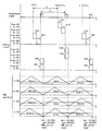
- FIG. 1 is a schematic configuration diagram of a power conversion device according to a first embodiment of the present invention.
- the power conversion device 1 converts power input from an external power supply 300 and outputs the converted power to an external load 400. Further, the power conversion device 1 includes a plurality of cells 101 to 104 and a central control device 200 that controls them. Although FIG. 1 shows an example in which four cells are used, the number is arbitrary.
- the cells 101 to 104 include first converters 141 to 144 and first control circuits 211 to 214 for controlling them, second converters 151 to 154, second control circuits 221 to 224 for controlling them, and Transformers 131 to 134 connected respectively between the converters 141 to 144 and the second converters 151 to 154 are provided.
- the first converters 141 to 144 and the first control circuits 211 to 214 are collectively defined as primary circuits 111 to 114, respectively.
- the second converters 151 to 154 and the second control circuits 221 to 224 are collectively defined as secondary circuits 121 to 124, respectively.
- the transformers 131 to 134 electrically insulate the primary side circuits 111 to 114 and the secondary side circuits 121 to 124, respectively. A more detailed configuration of the cell will be described later.
- the input terminals (input sides) of the cells 101 to 104 are connected in parallel to the power supply 300. Therefore, the input voltages of the cells 101 to 104 are all equal.
- the cells 101 to 104 convert the voltage of the power supply 300 to generate output voltages V O1 to V O4 , respectively.
- the first converter 141 of the primary side circuit 111 converts the voltage of the power supply 300 into an alternating voltage and applies it to the primary winding of the transformer 131.
- the first control circuit 211 of the primary side circuit 111 performs calculation and processing related to this operation to drive the first converter 141.
- the second converter 151 of the secondary side circuit 121 converts the voltage generated in the secondary winding of the transformer 131 to generate the voltage V O1 .
- the second control circuit 221 of the secondary side circuit 121 performs operation and processing related to this operation to drive the second converter 151. Also for cells 102 to 104, voltages V O2 to V O4 are respectively generated in the same manner.
- the output terminals (output side) of the cells 101 to 104 are connected in series with one another.
- the output voltage of the power conversion device 1 is a voltage obtained by combining the voltages V O1 to V O4 .
- the secondary side circuits 121 to 124 respectively control the output voltages V O1 to V O4 using PWM (Pulse Width Modulation) as described later.
- the second control circuit 221 performs PWM processing using a carrier signal generated internally and a duty ratio (hereinafter abbreviated as duty) transmitted from the outside, and drives the second converter 151 according to the result.
- the duty is a numerical value for setting the on period ratio of the switching element in PWM.
- the duty is generated by central controller 200 to control voltage V O1 to a desired value.
- the second control circuits 222 to 224 similarly perform PWM processing to drive the second converters 152 to 154, respectively.
- carrier signal generation by the second control circuits 221 to 224 is independent, PWM synchronization is realized by the method described later.
- the central control unit 200 performs all the PWM processing of the secondary side circuits 121 to 124, and A configuration in which the gate signal is transmitted to the secondary side circuits 121 to 124 is also conceivable.
- the central control unit 200 transmits the duty to the second control circuits 221 to 224 and the second control circuits 221 to 224 independently perform the PWM processing. It is possible to suppress the increase in complexity and cost of wiring relating to the control signal from central controller 200 to each cell.
- the central control unit 200 controls the output voltages V O1 to V O4 of the cells 101 to 104 in order to control the combined output voltage V OS to a desired value.
- the current detector 230 is disposed on the path of the output current.
- the control calculation unit 201 included in the central control unit 200 performs calculation of feedback control using the detected value of the output current detected from the current detector 230, and calculates the target value of the output voltage V OS and thus each output cell 101 to 104. Target values of voltages V O1 to V O4 are generated.
- control calculation unit 201 performs calculation and processing for setting the voltages V O1 to V O4 as target values, and the first control circuits 211 to 214 and the second control circuits 221 to 224 of the respective cells 101 to 104 Generate control commands.
- the control command is a target value (command value) of control or a state command such as start or stop, and the above-described duty is also included in the control command.
- the control operation unit 201 outputs the generated control command to the control signal transmission unit 202.
- the control signal transmission unit 202 generates a first control signal for each of the cells 101 to 104 based on the control command, and transmits the first control signal to the first control circuit 211 to 214 of each of the cells 1101 to 104.
- the first control signal transmitted by the control signal transmission unit 202 includes a control instruction to the second control circuits 221 to 224 like a duty. As described above, even the control command directed to the second control circuits 221 to 224 is temporarily transmitted to the first control circuits 211 to 214 of the cells 101 to 104 to which the second control circuits 221 to 224 belong.
- relay is performed using the first control circuits 211 to 214, and a control command is transmitted to the second control circuits 221 to 224.
- the primary side circuits 111 to 114 of the cells 101 to 104 are connected in parallel to the external power supply 300. Therefore, the ground potentials of the first control circuits 211 to 214 (reference potentials at which the circuits operate) are all common. Further, the ground potentials of the central control unit 200 and the first control circuits 211 to 214 can be shared. Therefore, for communication from the central control unit 200 to the first control circuits 211 to 214, insulation is not necessary, and communication using electric wires can be applied.
- serial communication is assumed as a communication method from the control signal transmission unit 202 of the central control device 200 to the first control circuits 211 to 214. Therefore, the first control signal is a serial communication signal of several bytes.
- FIG. 1 shows one arrow as the first control signal output from the control signal transmission unit 202, and shows a configuration in which it is input in parallel to the first control circuits 211 to 214 of each cell.
- the first control signal includes an address for identifying the cells 101 to 104. For this reason, the control signal transmission unit 202 encodes the control command and further adds an address to generate a serial communication signal.
- control signal transmission unit 202 outputs a synchronization instruction to synchronization signal transmission unit 203.
- the synchronization signal transmission unit 203 generates a synchronization signal based on the synchronization command output from the synchronization signal transmission unit 202, and outputs the synchronization signal to the first control circuits 211 to 214.
- the synchronization signals output to the first control circuits 211 to 214 are digital signals used for PWM synchronization, and the details will be described later.
- the synchronization signal transmission unit 203 of the central control device 200 outputs a common synchronization signal to all of the first control circuits 211 to 214.
- one arrow is shown as the synchronization signal output from the synchronization signal transmission unit 203, and the configuration to input it in parallel to the first control circuits 211 to 214 is shown.
- the ground potential can be made common, insulation is not necessary for all signal transmission from the central control unit 200 to each of the cells 101 to 104, which is not expensive optical fiber but inexpensive. Since electric wires can be used, a low cost power converter can be realized.
- the communication buses are shared among all the cells 101 to 104, the number of output ports of central control apparatus 200 can be reduced, and a lower cost power converter can be realized. There is also an advantage in terms of suppressing the complexity of the wiring.
- the first control circuit 211 extracts a control command related to the first converter 141 from the received first control signal, and drives the first converter 141 accordingly. Further, the first control circuit 211 extracts a control command (such as a duty) for the second converter 151 from the first control signal, generates a second control signal based on the extracted control command, and generates a second control generated. A signal is sent to the second control circuit 221. Communication from the first control circuit 211 to the second control circuit 221 is triggered by the rise (or fall) of the synchronization signal transmitted from the synchronization signal transmission unit 203 of the central control device 200.
- a control command such as a duty
- the first control circuits 212 to 214 also drive the first converters 142 to 144 in the same manner as the above-described first control circuit 211, and transmit the second control signals to the second control circuits 222 to 224, respectively. .
- the first control circuits 211 to 214 perform second control. Communication to circuits 221-224 is simultaneously performed in all cells 101-104. As described later, the second control circuits 221 to 224 of each of the cells 101 to 104 use the reception of the second control signal as a trigger to reset the carrier signal. Thus, PWM synchronization can be realized.
- serial communication is used as communication means from the first control circuits 211 to 214 of the cells 101 to 104 to the second control circuits 221 to 224. Therefore, the second control signal is a serial communication signal of several bytes.
- the ground potentials of the second control circuits 221 to 224 are different from each other.
- the ground potentials of the first control circuits 211 to 214 and the second control circuits 221 to 224 are also different. Therefore, the communication from the first control circuits 211 to 214 of the cells 101 to 104 to the second control circuits 221 to 224 requires insulation. Therefore, for example, communication using an optical fiber can be considered. However, since the communication is performed inside the cells 101 to 104, the total length of the optical fibers becomes relatively short, and the cost of the optical fibers can be reduced.
- communication from the first control circuits 211 to 214 to the second control circuits 221 to 224 in each of the cells 101 to 104 is a relatively short distance, in addition to the optical fiber, it may be similar to IrDA (Infrared Data Association). Infrared communication, ultrasonic waves, etc. may be used. In the case of infrared communication or ultrasonic communication, even if the ground potentials of the first control circuits 211 to 214 and the second control circuits 221 to 224 are largely different, the distance between the transceivers of infrared communication or ultrasonic communication can be set. It is possible to communicate while securing the insulation by structural means such as keeping appropriate.
- the external power source 300 may be either a DC power source or an AC power source.
- the external power supply 300 is a solar cell.
- the external load 400 there is a high voltage motor and other power devices.
- the external load 400 may be a power system as in the case of applying the power conversion device 1 to a PCS of solar power generation.
- Power converter 1 may be provided with elements, such as components for protection (relays, fuses, etc.) and components for filters (reactors, capacitors), in addition to the configuration described above.
- FIG. 2 is a diagram showing an example of the circuit configuration of the cell 101. As shown in FIG. In the example shown in FIG. 2, it is assumed that the external power supply 300 is a DC power supply, and the power conversion apparatus outputs AC power to the external load 400. The same configuration as that of the cell 101 shown in FIG. 2 can be applied to the other cells 102 to 104.
- the first converter 141 comprises a first inverter consisting of four switching elements (MOSFETs in the example of FIG. 2) 11-14.
- the direct current input terminal of the first inverter serves as the input terminal of the first converter 141.
- a filter capacitor 10 is connected between the DC input terminals of the first inverter.
- a series resonance circuit in which the primary winding of the coil 15, the capacitor 16 and the transformer 131 is connected in series is connected.
- the second converter 151 includes a diode bridge consisting of diodes 21 to 24.
- the secondary winding of the transformer 131 is connected between the AC input terminals of the diode bridge.
- the first inverter, the series resonant circuit, and the diode bridge described above constitute a resonant converter which is a type of isolated DC-DC converter.
- a smoothing capacitor 20 is connected between the DC output terminals of the diode bridge in the second converter 151.
- the second converter 151 includes a second inverter including four switching elements (MOSFETs in FIG. 2) 31 to 34.
- the AC output terminal of the second inverter serves as the output terminal of the second converter 151 of the cell 101.
- each of the cells 101 to 104 is composed of a resonant converter (hereinafter, converter) and a second inverter (hereinafter, inverter).
- converter resonant converter
- inverter second inverter
- the converter converts the voltage input to the cell 101 to generate a DC link voltage Vdc1 .
- the DC link voltage V dc1 can be controlled to a desired value by the on / off operation of the switching element.
- a voltage detector 25 for detecting the voltage V dc1 is arranged in FIG. Further, although not shown in FIG. 1, the detected voltage V dc1 is once taken into the second control circuit 221, and then transmitted from the second control circuit 221 to the first control circuit 211.
- the first control circuit 211 performs feedback control of the voltage V dc1 and drives the converter based on the result.
- the cells 102 to 104 also include a converter, and generate DC link voltages V dc2 to V dc4 , respectively.
- the DC link voltages V dc1 to V dc4 may all be controlled to the same value, or may be controlled to different values. However, in the following, it is assumed that the DC link voltages V dc1 to V dc4 are all controlled to the same value V dc .
- any specific circuit system can be applied as long as it is an isolated DC-DC converter.
- a rectifier circuit (AC-DC converter) may be added to the front stage of the converter of FIG.
- the inverter converts the voltage V dc1 to generate the output voltage V 01 of the cell 101.
- the cells 102 to 104 also include inverters, and convert the voltages V dc2 to V dc4 to generate voltages V 02 to V 04 , respectively.
- the inverters of the secondary side circuits 121 to 124 of the cells 101 to 104 control the output voltages V 01 to V 04 to desired values by PWM.
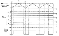
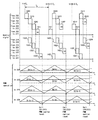
- FIGS. 3 and 4 are diagrams showing examples of PWM operation waveforms of the secondary side circuit 121 in the cell 101.
- FIG. FIG. 3 shows a PWM operation waveform when the voltage V 01 is controlled to a positive value. Specifically, as the PWM operation waveform, the carrier signal, the duty D 1 , the gate signal of the switching elements 31 to 34 and the V 01 waveform are shown. In addition, in FIG. 3, the dead time of the switching element is omitted for simplification of the drawings and the description.
- a triangular wave signal is shown as a carrier signal of PWM.
- the instantaneous value of the carrier signal changes in the range of 0 (0%) to 1 (100%).
- FIG. 3 shows PWM operation waveforms for three cycles of the carrier signal. In FIG. 3, the reset of the carrier signal described later is omitted.
- Duty D 1 is a control command for controlling the voltage V 01 to a desired value, is transmitted to the second control circuit 221 from the control signal transmitting unit 202 of the central controller 200 via the first control circuit 211 It is included in the control signal.
- Duty D 1 is a value from -1 (-100%) to +1 (+ 100%).
- the duty D 1 has a value from 0 to +1.
- Figure 3 between each period of the carrier signal, it was assumed that the duty D 1 is constant. Also, the case is shown where the duty D 1 gradually increases over three cycles of the carrier signal.
- switching elements 33 and 34 shown in FIG. 2 are controlled to be off and on, respectively.
- Switching elements 31 and 32 are on-off controlled according to the comparison result of the duty D 1 and the carrier signal. During the period the duty D 1 is greater than the carrier signal, the switching element 31 and 32 are controlled to turn on and off, (instantaneous value of) the voltage V 01 becomes + V dc. In duty D 1 is smaller period than the carrier signal, the switching element 31 and 32 are controlled to off and on, (instantaneous value of) V 01 becomes zero.
- the average value of the voltage V 01 in the carrier period is (D 1 V dc ). If the duty D 1 is changed in the range of 0 to +1, the inverter can output a desired voltage in the range of 0 ⁇ V 01 ⁇ + V dc as an average value in the carrier period. As in the example shown in FIG. 3, as the duty D 1 increases, the voltage V 01 (average value in the carrier period) also increases.
- FIG. 4 is a PWM operation waveform diagram in the case of controlling the voltage V 01 to a negative value.
- the duty D 1 takes a value from ⁇ 1 ( ⁇ 100%) to 0.
- showed
- the switching elements 31 and 32 are controlled to be off and on, respectively.
- the switching elements 33 and 34 are on / off controlled according to the comparison result of the absolute value
- the switching elements 33 and 34 are controlled to be on and off, respectively, and the voltage V 01 (the instantaneous value thereof) becomes ⁇ V dc .
- the switching elements 33 and 34 are controlled to be off and on, respectively, and the voltage V 01 (the instantaneous value thereof) becomes zero.
- the average value of the voltage V 01 in the carrier period is (D 1 V dc ).
- the utility D 1 is a negative value. If the duty D 1 is changed in the range of ⁇ 1 to 0, the inverter can output a desired voltage in the range of ⁇ V dc ⁇ V 01 ⁇ 0 as an average value in the carrier period. As in the example shown in FIG. 4, as
- the duty may be set to (V a / V dc ) with respect to the target value V dc of the DC link voltage.
- ⁇ V dc ⁇ V a ⁇ + V dc .
- control operation unit 201 generates target value V dc and duty (V a / V dc ) as control commands, and control signal transmission unit 202 generates a first control signal based on these control commands.
- Vdc is a fixed value and is recorded in both the central control unit 200 and the first control circuit 211.
- control operation unit 201 of the central control device 200 may also generate data (symbol) representing start or operation continuation of the converter as a control command. Also in the cells 102 to 104 (secondary circuits 122 to 124), the PWM processing is performed in the same manner.
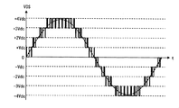
- FIG. 5 is a diagram showing an example of the combined output voltage V OS waveform. 5, the sine wave indicated by a broken line is a basic wave component contained in the combined output voltage V OS, may be considered as a target value of the combined output voltage V OS.
- the instantaneous value of the combined output voltage V OS is, -4V dc, -3V dc, ⁇ , 0, ⁇ , + 3V dc, made with any of the + 4V dc.
- power converter 1 as an average value in the carrier period, to output a desired voltage in the range of -4V dc ⁇ V OS ⁇ + 4V dc.
- FIG. 5 when the target value of the combined output voltage V OS is changed in a sinusoidal manner, a multi-level pseudo-sinusoidal combined output voltage V OS is generated.
- FIG. 6 is a timing chart showing the principle of PWM synchronization. Specifically, in FIG. 6, the synchronization signal waveform, the first control signal directed from the control signal transmission unit 202 of the central control unit 200 to the first control circuit 211 to 214 of each of the cells 101 to 104, each of the cells 101 to 104. Shows second control signals respectively transmitted from the first control circuits 211 to 214 to the second control circuits 221 to 224, and PWM operation waveforms performed in the second control circuits 221 to 224 of the respective cells 101 to 104. .
- the first control signal directed from the control signal transmission unit 202 of the central control device 200 to the first control circuit 211 is the first control circuit 211 among the first control signals transmitted from the control signal transmission unit 202. Means an address given.
- carrier signals generated by the second control circuits 221 to 224 and duties D 1 to D 4 are shown as PWM operation waveforms of the cells 101 to 104.
- Duty D 2 to D 4 is a control command for controlling V 02 to V 04 to a desired value, and from the control signal transmitting unit 202 of the central control unit 200 via the first control circuits 212 to 214, respectively. 2 included in the control signal transmitted to each of the control circuits 222 to 224.
- the specific values of the duties D 1 to D 4 in FIG. 6 are not values that are assumed to obtain the waveform of FIG. 5. Moreover, illustration is abbreviate
- T S represents a control cycle of central control unit 200. Specifically, it is a cycle in which the control operation unit 201 performs control operation and transmits the first control signal from the control signal transmission unit 202 to each of the cells 101 to 104.
- k is an integer representing a discrete time step.
- the control signal transmission unit 202 of the central control device 200 starts transmitting the first control signal to the first control circuits 211 to 214 of the cells 101 to 104.
- the control signal transmission unit 202 of the central control unit 200 The first control signal 1014 directed to the control circuit 214 is first transmitted.
- the first control signal 1013 directed to the first control circuit 213, the first control signal 1012 directed to the first control circuit 212, and the first control signal 1011 directed to the first control circuit 211 are sequentially transmitted.
- the control signal transmission unit 202 of the central control device 200 After transmitting the first control signal 1011 directed to the first control circuit 211, the control signal transmission unit 202 of the central control device 200 outputs a synchronization command to the synchronization signal transmission unit 203.
- the synchronization signal transmission unit 203 sets the synchronization signal, which is a digital signal, to H level in response to the reception of the synchronization command from the control signal transmission unit 202, and generates a rising edge of the synchronization signal.
- the rising of the synchronization signal occurs simultaneously with the completion of the transmission of the first control signal 1011, disregarding the processing delay during this period.
- the rising edge of the synchronization signal is output to the first control circuits 211 to 214 of all the cells 101 to 104.
- the first control circuits 211 to 214 of the cells 101 to 104 respectively transmit the second control signals 1021 to 1024 to the second control circuits 221 to 224 using the rising edge of the synchronization signal as a trigger. As mentioned above, these communications are simultaneously performed in all the cells 101 to 104.
- the second control signals 1021 to 1024 include information on the duties D 1 (k) to D 4 (k), respectively.
- the second control circuits 221 to 224 of each of the cells 101 to 104 use the reception of the second control signal as a trigger to reset the carrier signal.
- the value of the carrier signal generated by the second control circuit of each cell is initialized to 0 simultaneously with the completion of reception of the second control signal at time points t1, t2 and t3, and thereafter increases to 1 Begin (horizontal dashed line in FIG. 6 indicates "1").
- the reset of the carrier signal is also performed simultaneously for all the cells 101 to 104.
- the received D 1 (k) to D 4 (k) are reflected in the duty of each of the cells 101 to 104 after the reset.
- the cycle in which the rising of the synchronization signal occurs is T S as in the control cycle.
- Carrier period of each cell 101-104 is set to the same time as the control period T S of the central control unit 200.
- the carrier periods of the cells 101 to 104 do not have exactly the same time.
- the rising period T S of the synchronization signal does not have exactly the same value.
- the central control unit 200 and the second control circuits 221 to 224 perform computation, communication, PWM processing and the like by a digital control unit (microcomputer, digital signal processor, etc.).
- a digital control unit microcomputer, digital signal processor, etc.
- the carrier cycle of the second control circuit 221 is slightly shorter than T S
- the carrier cycle of the second control circuit 222 is slightly longer than T S of the central control unit 200.
- the carrier signals of the cells 101 to 104 can be substantially synchronized by simultaneously resetting the carrier signals of all the cells 101 to 104 as in the first embodiment. That is, as shown in FIG. 6, immediately before time t1, the carrier signals of the second control circuits 221 to 224 are gradually delayed as going from the second control circuits 221 to 224. For this reason, the carrier signals of the cells 101 to 104 can be substantially synchronized by simultaneously resetting the carrier signals of the second control circuits 221 to 224 at time t1.
- a cyclic error of the carrier signals of the second control circuits 221 to 224 occurs, but at time t2 by simultaneously resetting the carrier signals of the second control circuits 221 to 224.
- the carrier signals of the cells 101 to 104 can be approximately synchronized.
- the timing t3 is also similar to the timings t1 and t2.
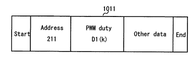
- FIG. 7 is a diagram showing a specific data configuration example of the first control signal 1011 shown in FIG.
- the first control signal 1011 is a serial communication signal of several bytes. Specifically, it comprises a start bit, an address portion, a duty portion, another data portion (Other data), and an end bit (stop bit).
- the address portion following the start bit is configured as digital data for identifying the first control circuit 211 of the cell 101.
- the duty part (PWM duty) is configured as digital data for indicating the value of the duty D 1 (k) shown in FIG.
- the other data portion (Other data) is constituted by digital data, parity bits or the like for indicating the contents of control commands other than duty. The existence and contents of other data parts can be set arbitrarily.
- FIG. 8 is a diagram showing a specific data configuration example of the second control signal 1021 shown in FIG.
- the second control signal 1021 is a serial communication signal of several bytes. Specifically, it comprises a start bit, a duty part (PWM duty), another data part, and an end bit (stop bit). Since the communication is performed inside the cell, the address part is unnecessary.
- the duty part is configured as digital data for indicating the value of the duty D 1 (k) shown in FIG. 6, and may have the same content as the duty part of the first control signal 1011 shown in FIG.
- the other data portion is composed of digital data for indicating the contents of control commands other than duty, or parity bits. The existence and contents of other data parts can be set arbitrarily.
- FIG. 9 is a view showing a configuration example of the first control circuit 211 of the cell 101. As shown in FIG. The same configuration can be applied to the first control circuits 212 to 214 of the other cells 102 to 104.
- the first control circuit 211 includes a control signal reception unit 2111, a synchronization signal reception unit 2112, a control signal transmission unit 2113, and a drive control unit 2114.
- the control signal reception unit 2111 receives the first control signal transmitted from the control signal transmission unit 202 of the central control device 200, and confirms the address of the first control signal. When it is determined that the first control signal is directed to the first control circuit 211, the control command contained in the first control signal is extracted and the following processing is performed.
- a control command to the second control circuit 221 is output to the control signal transmission unit 2113 like a duty.
- a control command for the first converter 141 of the primary side circuit 111 is output to the drive control unit 2114.
- the synchronization signal reception unit 2112 detects the rising edge of the synchronization signal transmitted from the synchronization signal transmission unit 203 of the central control device 200, and outputs a transmission command to the control signal transmission unit 2113.
- the control signal transmission unit 2113 generates a second control signal based on the control command to the second control circuit 221 output by the control signal reception unit 2111. After that, it transmits to the second control circuit 221 according to the transmission command output from the synchronization signal reception unit 2112.
- the drive control unit 2114 drives and controls the first converter 141 in accordance with the control command on the first converter 141 output from the control signal receiving unit 2111.
- FIG. 10 is a diagram showing a configuration example of the second control circuit 221 of the cell 101. As shown in FIG. The same configuration as that of the second control circuit 221 can be applied to the second control circuits 222 to 224 of the other cells 102 to 104.
- the second control circuit 221 includes a control signal reception unit 2211, a carrier signal generation unit 2212, and a drive control unit 2213.
- the control signal receiving unit 2211 receives the second control signal transmitted from the first control circuit 211, extracts a duty that is a control command, and outputs the extracted duty to the drive control unit 2213. Further, the control signal receiving unit 2211 outputs a reset command to the carrier signal generating unit 2212 simultaneously with the completion of the reception of the second control signal.
- the carrier signal generation unit 2212 generates a carrier signal at a set carrier cycle, and outputs the carrier signal to the drive control unit 2213. Also, at the same time as receiving a reset command from the control signal receiving unit 2211, the carrier signal is reset.
- the drive control unit 2213 compares the duty from the signal reception unit 2211 with the carrier signal from the carrier signal generation unit 2212, and drives and controls the second converter 151 based on the result.
- FIG. 11 is a timing chart showing another example of PWM synchronization. Only the difference from the PWM synchronization described in FIG. 6 will be described below.
- the configuration shown in FIG. 11 for resetting the carrier signal after a predetermined time T W has passed since the second control circuits 221 to 224 have received the second control signal is different from all the embodiments described below. It can be applied as
- the duty is transmitted from the central control unit 200 to the second control circuits 221 to 224 and the second control circuits 221 to 224 independently perform the PWM processing.
- the primary side circuits 111 to 114 of the cells 101 to 104 are connected in parallel to the external power supply 300, and the ground potentials of the first control circuits 211 to 214 are all common.
- the ground potentials of the central control unit 200 and the first control circuits 211 to 214 can also be shared. Therefore, for communication from the central control unit 200 to the first control circuits 211 to 214, insulation is not necessary, communication using an electric wire can be applied, and the cost for insulation processing can be omitted.
- the power conversion apparatus when used for an inverter for driving a high voltage motor or PCS for a high voltage distribution system, a withstand voltage exceeding 5 kV is required unless the first embodiment of the present invention is applied. It is expensive.
- a low cost power converter that performs PWM synchronization can be realized.
- FIG. 12 is a timing chart showing the principle of PWM synchronization in the second embodiment.
- the configuration of the power conversion device in the second embodiment is the same as the configuration of the first embodiment shown in FIG. 1, and therefore the illustration and the detailed description will be omitted.
- the second control signal transmitted to each of the control circuits 221 to 224 includes information of a reset command in addition to the duty as a control command.
- the reset command is a 1-bit control command which is information indicating whether the second control circuits 221 to 224 reset the carrier signal after receiving the control signal (on or off).
- the first control circuit 211 directed from the control signal transmission unit 202 of the central control unit 200 to the first control circuit 211
- the reset command of the first control signal 1311 is turned on as described above.
- the first control circuit 211 of the cell 101 After receiving the first control signal 1311, the first control circuit 211 of the cell 101 transmits a second control signal 1321 to the second control circuit 221 using the rising edge of the synchronization signal as a trigger. At this time, in response to the reset command of the first control signal 1311 being on, the reset command of the second control signal 1321 is also turned on.
- the second control circuit 221 resets the carrier signal using the reception of the second control signal 1321 as a trigger in response to the reset command of the second control signal 1321 being on.
- the first control signal 1411 directed from the control signal transmitting unit 202 of the central controller 200 to the first control circuit 211 does not turn on the reset command (Although illustration is omitted, the reset command is set to off). Therefore, the reset command is also set to OFF for the second control signal 1421 from the first control circuit 211 to the second control circuit 221.
- the second control circuit 221 In response to the reset instruction of the second control signal 1421 being off, the second control circuit 221 does not reset the carrier signal even if the second control signal 1421 is received.
- the second embodiment is slightly different from the first embodiment in the configuration and operation of the first control circuits 211 to 214 and the second control circuits 221 to 224. However, since the operation has been described above, FIG. The illustration of a block diagram such as 10 is omitted.
- the carrier signal is reset in every control cycle, but as in the second embodiment, the carrier cycle of each of the cells 101 to 104 and the control cycle T S of the central control unit 200 Is sufficiently small, the carrier signals of each cell can be substantially synchronized even if the carrier signals are not reset in all control cycles.
- the second embodiment is applicable to one in which the operation level of the control unit such as a microcomputer is lower than that of the first embodiment.
- the control unit such as a microcomputer
- FIG. 13 is a timing chart showing the principle of PWM synchronization in the third embodiment.
- the configuration of the power conversion device according to the third embodiment is the same as the configuration of the first embodiment shown in FIG. 1 and thus the illustration and the detailed description will be omitted.
- the control signal transmission unit 202 of the central control device 200 transmits only the first control signal 1114 directed to the first control circuit 214 and the first control signal 1113 directed to the first control circuit 213 in order.
- the central control device 200 completes the calculation of the duty by communicating the control signal and resetting the carrier signal as shown in FIG.
- the time until the duty is reflected in the second control circuit, that is, the delay time by communication can be shortened.
- FIG. 14 is a schematic configuration diagram of a power conversion device in a fourth embodiment. Hereinafter, only differences from the power conversion device 1 in the first embodiment described with reference to FIG. 1 will be described.
- the power conversion device 2 shown in FIG. 14 includes a central control unit 204 instead of the central control unit 200 of FIG.
- the central control unit 204 of FIG. 14 does not include the synchronization signal transmission unit 203 as compared with the central control unit 200 of the first embodiment, and the synchronization control signal is sent to the first control circuits 211 to 214 of 101 to 104 of each cell. It is configured not to output.
- FIG. 15 is a timing chart showing the principle of PWM synchronization in the fourth embodiment.
- the control signal includes a reset command.
- the difference from the PWM synchronization in the second embodiment described with reference to FIG. 12 will be described.
- control signal transmission unit 202 of the central control unit 204 transmits the first control signal directed to the first control circuits 211 to 214 at each control cycle.
- the control signal transmission unit 202 performs the output of the first control signal four times (for four frames) per control cycle, but the first control signal of the fourth in time (the first control signals 1311, 1412 and 1513 in FIG. 15) Set the reset command to on for.
- the address in the fourth first control signal is rotated among the first control circuits 211 to 214 of the cells 101 to 104.
- the address in the fourth control signal changes to the cell 101 (first control circuit 211), the cell 102 (first control circuit 212), and the cell 103 (first control circuit 213).
- the first control circuits 211 to 214 of each of the cells 101 to 104 receive the first control signal transmitted by the control signal transmission unit 202 of the central control device 200, and immediately receive the second control signal to the second control circuits 221 to 224. Send After receiving the second control signal, the second control circuits 221 to 224 of each of the cells 101 to 104 reset the carrier signal if the reset command is on.
- the time from the starting point of the control cycle (the time when communication of the first control signal by the control signal transmission unit 202 starts) to the reset of the carrier signal can be kept constant, as shown in FIG. realizable.
- the configuration of the central control unit 204 and the wiring from the central control unit 204 to each of the cells 101 to 104 can be simplified as much as the synchronization signal is not used.
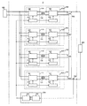
- FIG. 16 is a schematic configuration diagram of a power conversion device in a fifth embodiment of the present invention.
- the power conversion device 3 of FIG. 16 includes four cells 105 to 108.
- the difference between the first embodiment and the fifth embodiment shown in FIG. 1 is that the input terminals (input sides) of the cells 105 to 108 are connected in series, and the combined input terminal is connected to the external power supply 301.
- the output terminals (output side) of the cells 105 to 108 are connected in parallel to the load 401.
- the cells 105 to 108 include primary circuits 115 to 118, secondary circuits 125 to 128, and transformers 135 to 138, respectively.
- the primary side circuits 115 to 118 include second converters 155 to 158 and second control circuits 225 to 228 for controlling them, and the secondary side circuits 125 to 128 include first converters 145 to 148 and The first control circuits 215 to 218 that control these are provided, respectively, and the internal configuration of the cells 105 to 108 is the same as that of the cells 101 to 104 of the first embodiment, so The PWM synchronization can be applied to the fifth embodiment as it is.
- the configuration of the fifth embodiment can be applied to a power converter that converts the primary side to a high voltage of, for example, 66 kv and converts the secondary side to a low voltage of, for example, 100 v.
- Sixth Embodiment A sixth embodiment of the present invention is an example in which three power conversion devices 1 described in the first embodiment are used to configure a three-phase AC power conversion device.
- FIG. 17 is a schematic configuration diagram of the power conversion device 4 in the sixth embodiment.
- the power conversion device 4 shown in FIG. 17 includes three power conversion devices 1 described in the first embodiment.
- one of the output terminals provided in the three power electronics devices 1 constitutes a three-phase output terminal, and is connected to the three-phase load 401.
- the other (one other) of the output terminals provided in the three power electronics devices 1 are connected to one another to form a neutral point in the Y-connected three-phase AC circuit.
- the input terminals of the three power electronics devices 1 are connected in parallel to each other and connected to the power supply 300.
- the power conversion device 1 includes the central control device 200 therein. Therefore, although the power conversion device 4 of FIG. 17 is provided with three central control devices 200, the three central control devices 200 may be integrated into one.
- the sixth embodiment of the present invention can be applied to, for example, an inverter for driving a three-phase high voltage motor or a three-phase AC power system PCS, and is also an embodiment of a power converter outputting three-phase AC. An effect similar to 1 can be obtained.
- the plurality of cells 101 to 104 are connected in parallel to the external power supply 300 and connected in series to the external load 400
- the fifth embodiment includes the plurality of cells 105.
- 108 to 108 are connected in series to the external power supply 301 and in parallel to the load 401
- a plurality of cells are connected in series to the external power supply and are also connected in series to the load. Even if there are, the present invention is applicable.
Landscapes
- Engineering & Computer Science (AREA)
- Power Engineering (AREA)
- Inverter Devices (AREA)
- Dc-Dc Converters (AREA)
Priority Applications (1)
| Application Number | Priority Date | Filing Date | Title |
|---|---|---|---|
| CN201880057590.8A CN111052587B (zh) | 2017-12-14 | 2018-11-06 | 电力转换装置 |
Applications Claiming Priority (2)
| Application Number | Priority Date | Filing Date | Title |
|---|---|---|---|
| JP2017-239435 | 2017-12-14 | ||
| JP2017239435A JP6951228B2 (ja) | 2017-12-14 | 2017-12-14 | 電力変換装置 |
Publications (1)
| Publication Number | Publication Date |
|---|---|
| WO2019116785A1 true WO2019116785A1 (ja) | 2019-06-20 |
Family
ID=66820137
Family Applications (1)
| Application Number | Title | Priority Date | Filing Date |
|---|---|---|---|
| PCT/JP2018/041154 Ceased WO2019116785A1 (ja) | 2017-12-14 | 2018-11-06 | 電力変換装置 |
Country Status (3)
| Country | Link |
|---|---|
| JP (1) | JP6951228B2 (https=) |
| CN (1) | CN111052587B (https=) |
| WO (1) | WO2019116785A1 (https=) |
Cited By (3)
| Publication number | Priority date | Publication date | Assignee | Title |
|---|---|---|---|---|
| CN113809924A (zh) * | 2020-06-12 | 2021-12-17 | 平高集团有限公司 | 一种多级单元通讯同步的电力电子变压器 |
| CN115224918A (zh) * | 2021-04-20 | 2022-10-21 | 富士电机株式会社 | 电力转换装置 |
| US12160182B2 (en) | 2021-06-08 | 2024-12-03 | Honda Motor Co., Ltd. | Power conversion device, method of controlling power conversion device, and storage medium |
Families Citing this family (2)
| Publication number | Priority date | Publication date | Assignee | Title |
|---|---|---|---|---|
| CN114079382B (zh) * | 2020-08-11 | 2025-09-05 | 富士电机株式会社 | 电力转换装置 |
| JP7714875B2 (ja) * | 2020-08-11 | 2025-07-30 | 富士電機株式会社 | 電力変換装置 |
Citations (5)
| Publication number | Priority date | Publication date | Assignee | Title |
|---|---|---|---|---|
| JP2012100398A (ja) * | 2010-11-01 | 2012-05-24 | Hitachi Ltd | 電力変換装置 |
| JP2015100262A (ja) * | 2013-11-19 | 2015-05-28 | エルエス産電株式会社Lsis Co., Ltd. | 並列インバータ制御装置 |
| JP2017123781A (ja) * | 2012-01-17 | 2017-07-13 | インフィネオン テクノロジーズ オーストリア アクチエンゲゼルシャフト | 電力変換回路および電力供給システム |
| JP2017216809A (ja) * | 2016-05-31 | 2017-12-07 | 東芝三菱電機産業システム株式会社 | 電力変換装置 |
| WO2017208322A1 (ja) * | 2016-05-31 | 2017-12-07 | 株式会社日立製作所 | 電力変換器セル及び電力変換装置 |
Family Cites Families (5)
| Publication number | Priority date | Publication date | Assignee | Title |
|---|---|---|---|---|
| CN1215636C (zh) * | 2001-12-31 | 2005-08-17 | 艾默生网络能源有限公司 | 确立多机并联系统中主机的方法 |
| KR100874639B1 (ko) * | 2007-03-16 | 2008-12-17 | 엘지디스플레이 주식회사 | 액정표시장치 |
| CN101388681B (zh) * | 2007-09-13 | 2012-11-14 | 东方通信股份有限公司 | 一种tetra收发信机及其实现方法 |
| JP2016187290A (ja) * | 2015-03-27 | 2016-10-27 | パナソニックIpマネジメント株式会社 | 電力供給システム及び電力変換装置 |
| CN105978554B (zh) * | 2016-06-30 | 2018-11-02 | 特变电工西安电气科技有限公司 | 一种并联型逆变器载波同步系统及同步方法 |
-
2017
- 2017-12-14 JP JP2017239435A patent/JP6951228B2/ja active Active
-
2018
- 2018-11-06 CN CN201880057590.8A patent/CN111052587B/zh active Active
- 2018-11-06 WO PCT/JP2018/041154 patent/WO2019116785A1/ja not_active Ceased
Patent Citations (5)
| Publication number | Priority date | Publication date | Assignee | Title |
|---|---|---|---|---|
| JP2012100398A (ja) * | 2010-11-01 | 2012-05-24 | Hitachi Ltd | 電力変換装置 |
| JP2017123781A (ja) * | 2012-01-17 | 2017-07-13 | インフィネオン テクノロジーズ オーストリア アクチエンゲゼルシャフト | 電力変換回路および電力供給システム |
| JP2015100262A (ja) * | 2013-11-19 | 2015-05-28 | エルエス産電株式会社Lsis Co., Ltd. | 並列インバータ制御装置 |
| JP2017216809A (ja) * | 2016-05-31 | 2017-12-07 | 東芝三菱電機産業システム株式会社 | 電力変換装置 |
| WO2017208322A1 (ja) * | 2016-05-31 | 2017-12-07 | 株式会社日立製作所 | 電力変換器セル及び電力変換装置 |
Cited By (4)
| Publication number | Priority date | Publication date | Assignee | Title |
|---|---|---|---|---|
| CN113809924A (zh) * | 2020-06-12 | 2021-12-17 | 平高集团有限公司 | 一种多级单元通讯同步的电力电子变压器 |
| CN113809924B (zh) * | 2020-06-12 | 2025-03-07 | 平高集团有限公司 | 一种多级单元通讯同步的电力电子变压器 |
| CN115224918A (zh) * | 2021-04-20 | 2022-10-21 | 富士电机株式会社 | 电力转换装置 |
| US12160182B2 (en) | 2021-06-08 | 2024-12-03 | Honda Motor Co., Ltd. | Power conversion device, method of controlling power conversion device, and storage medium |
Also Published As
| Publication number | Publication date |
|---|---|
| JP2019106825A (ja) | 2019-06-27 |
| CN111052587B (zh) | 2023-04-18 |
| JP6951228B2 (ja) | 2021-10-20 |
| CN111052587A (zh) | 2020-04-21 |
Similar Documents
| Publication | Publication Date | Title |
|---|---|---|
| EP3059847B1 (en) | Power conversion device and power conversion method | |
| WO2019116785A1 (ja) | 電力変換装置 | |
| DK3046203T3 (en) | Wind power converter system | |
| JP6194193B2 (ja) | 直流昇圧変換器、制御方法及びコンバータ部制御装置 | |
| EP2849332B1 (en) | Multilevel inverter | |
| EP2980977B1 (en) | Power converters for aircraft starter/generators | |
| US20150333642A1 (en) | High voltage direct current transmission system and controlling method thereof | |
| US20160380551A1 (en) | Converter arrangement having multi-step converters connected in parallel and method for controlling these | |
| US9379627B2 (en) | Power conversion circuit arrangements utilizing resonant alternating current linkage | |
| US11990830B2 (en) | Power conversion system and virtual DC voltage generator circuit | |
| JP5410551B2 (ja) | 電力変換装置 | |
| JP6601668B2 (ja) | 電力変換装置 | |
| JP5047210B2 (ja) | 電力変換装置 | |
| KR20200040027A (ko) | 복수의 컨버터 모듈을 구비하는 dc/dc 컨버터 | |
| JPH11252992A (ja) | 電力変換装置 | |
| US12294313B2 (en) | Drive system and control device for drive system | |
| KR102624204B1 (ko) | 반도체 변압기의 제어 방법 및 장치 | |
| KR102269005B1 (ko) | 발전기 시스템 | |
| KR20130110287A (ko) | 다중레벨 인버터 제어장치 | |
| JP2006238621A (ja) | 無停電電源装置 | |
| CN118573001B (zh) | 一种电机电源调节电路及控制方法、电子设备 | |
| EP4622081A1 (en) | Power supply device | |
| JP2019097323A (ja) | 電力変換装置、電力変換用制御装置および電力変換回路の制御方法 | |
| JP2019118194A (ja) | 変換器、電力制御方法、及びプログラム | |
| JP2017204976A (ja) | 電力変換装置 |
Legal Events
| Date | Code | Title | Description |
|---|---|---|---|
| 121 | Ep: the epo has been informed by wipo that ep was designated in this application |
Ref document number: 18888014 Country of ref document: EP Kind code of ref document: A1 |
|
| NENP | Non-entry into the national phase |
Ref country code: DE |
|
| 122 | Ep: pct application non-entry in european phase |
Ref document number: 18888014 Country of ref document: EP Kind code of ref document: A1 |