WO2019116785A1 - Power conversion device - Google Patents
Power conversion device Download PDFInfo
- Publication number
- WO2019116785A1 WO2019116785A1 PCT/JP2018/041154 JP2018041154W WO2019116785A1 WO 2019116785 A1 WO2019116785 A1 WO 2019116785A1 JP 2018041154 W JP2018041154 W JP 2018041154W WO 2019116785 A1 WO2019116785 A1 WO 2019116785A1
- Authority
- WO
- WIPO (PCT)
- Prior art keywords
- control
- power conversion
- control circuit
- signal
- converter
- Prior art date
Links
Images


Classifications
-
- H—ELECTRICITY
- H02—GENERATION; CONVERSION OR DISTRIBUTION OF ELECTRIC POWER
- H02M—APPARATUS FOR CONVERSION BETWEEN AC AND AC, BETWEEN AC AND DC, OR BETWEEN DC AND DC, AND FOR USE WITH MAINS OR SIMILAR POWER SUPPLY SYSTEMS; CONVERSION OF DC OR AC INPUT POWER INTO SURGE OUTPUT POWER; CONTROL OR REGULATION THEREOF
- H02M7/00—Conversion of ac power input into dc power output; Conversion of dc power input into ac power output
- H02M7/42—Conversion of dc power input into ac power output without possibility of reversal
- H02M7/44—Conversion of dc power input into ac power output without possibility of reversal by static converters
- H02M7/48—Conversion of dc power input into ac power output without possibility of reversal by static converters using discharge tubes with control electrode or semiconductor devices with control electrode
- H02M7/483—Converters with outputs that each can have more than two voltages levels
-
- H—ELECTRICITY
- H02—GENERATION; CONVERSION OR DISTRIBUTION OF ELECTRIC POWER
- H02M—APPARATUS FOR CONVERSION BETWEEN AC AND AC, BETWEEN AC AND DC, OR BETWEEN DC AND DC, AND FOR USE WITH MAINS OR SIMILAR POWER SUPPLY SYSTEMS; CONVERSION OF DC OR AC INPUT POWER INTO SURGE OUTPUT POWER; CONTROL OR REGULATION THEREOF
- H02M7/00—Conversion of ac power input into dc power output; Conversion of dc power input into ac power output
- H02M7/42—Conversion of dc power input into ac power output without possibility of reversal
- H02M7/44—Conversion of dc power input into ac power output without possibility of reversal by static converters
- H02M7/48—Conversion of dc power input into ac power output without possibility of reversal by static converters using discharge tubes with control electrode or semiconductor devices with control electrode
- H02M7/483—Converters with outputs that each can have more than two voltages levels
- H02M7/49—Combination of the output voltage waveforms of a plurality of converters
-
- Y—GENERAL TAGGING OF NEW TECHNOLOGICAL DEVELOPMENTS; GENERAL TAGGING OF CROSS-SECTIONAL TECHNOLOGIES SPANNING OVER SEVERAL SECTIONS OF THE IPC; TECHNICAL SUBJECTS COVERED BY FORMER USPC CROSS-REFERENCE ART COLLECTIONS [XRACs] AND DIGESTS
- Y02—TECHNOLOGIES OR APPLICATIONS FOR MITIGATION OR ADAPTATION AGAINST CLIMATE CHANGE
- Y02B—CLIMATE CHANGE MITIGATION TECHNOLOGIES RELATED TO BUILDINGS, e.g. HOUSING, HOUSE APPLIANCES OR RELATED END-USER APPLICATIONS
- Y02B70/00—Technologies for an efficient end-user side electric power management and consumption
- Y02B70/10—Technologies improving the efficiency by using switched-mode power supplies [SMPS], i.e. efficient power electronics conversion e.g. power factor correction or reduction of losses in power supplies or efficient standby modes
Definitions
- the present invention relates to a power converter.
- a power conversion device in which a plurality of power conversion cells (hereinafter referred to as cells) are connected in series or in parallel is used.
- a multiple power converter described in Patent Document 1.
- outputs of a plurality of inverter units are respectively connected in series to obtain a high voltage output.
- Patent Document 1 describes PWM (Pulse Width Modulation) of a plurality of inverter units.
- the on / off state of the semiconductor element (switching element) included in each inverter unit is controlled by using a plurality of carrier waves according to the number of inverter units.
- multistage (multilevel) output voltages can be obtained.
- a plurality of carrier signals are in phase with one another. Synchronizing the phases of a plurality of carrier signals is considered to be effective in suppressing harmonic components included in the output voltage. Moreover, it is considered effective also in suppressing that the output voltage changes a plurality of levels at once and adversely affecting the load such as a motor.
- Such a configuration of the power conversion device is effective when directly driving a high voltage motor.
- PCS power conditioning system
- a configuration using a plurality of cells is considered to be effective also in increasing the voltage and increasing the capacity of the PCS.
- PWM synchronization synchronization of phases of a plurality of carrier signals used for PWM of a plurality of cells.
- a configuration is conceivable in which the central control unit performs PWM processing of all the cells and transmits the generated gate signal of the switching element to the control circuit of each cell.
- a cell often includes a plurality of switching elements instead of one, a plurality of gate signal lines are provided according to the number of switching elements, which causes a problem of the complexity and cost increase of the power conversion device. It becomes.
- An object of the present invention is to realize a low cost power converter that performs PWM synchronization.
- the present invention is configured as follows.
- the power converter includes: a plurality of power conversion cells for converting a power supply voltage into a voltage for supplying a load; and a central control unit for controlling the plurality of power conversion cells, each of the plurality of power conversion cells being A first converter for converting the power supply voltage, a first control circuit for controlling the first converter, a second converter for converting the voltage converted by the first converter, and a second converter A second control circuit for controlling the pulse width modulation by pulse width modulation, and a transformer connected between the first converter and the second converter,
- the central control device includes a control signal transmission unit that transmits a first control signal to the first control circuit included in each of the plurality of power conversion cells, and based on the first control signal, the plurality of powers A first control circuit included in each of the conversion cells controls the first converter, and the second control circuit controls the second converter to reset the carrier signal of the pulse width modulation.
- a low cost power converter that performs PWM synchronization can be realized.
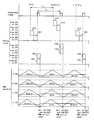
- FIG. 1 is a schematic configuration diagram of a power conversion device in a first embodiment. It is a figure which shows the circuit structural example of a cell. It is a figure which shows the PWM operation
- 5 is a timing chart showing the principle of PWM synchronization of the first embodiment. It is a figure which shows the specific data structural example of a 1st control signal. It is a figure which shows the specific data structural example of a 2nd control signal.
- FIG. 10 is a schematic configuration diagram of a power conversion device in a fourth embodiment. 15 is a timing chart showing the principle of PWM synchronization in the fourth embodiment.
- FIG. 13 is a schematic configuration diagram of a power conversion device in a fifth embodiment.
- FIG. 16 is a schematic configuration diagram of a power conversion device 4 in a sixth embodiment.
- FIG. 1 is a schematic configuration diagram of a power conversion device according to a first embodiment of the present invention.
- the power conversion device 1 converts power input from an external power supply 300 and outputs the converted power to an external load 400. Further, the power conversion device 1 includes a plurality of cells 101 to 104 and a central control device 200 that controls them. Although FIG. 1 shows an example in which four cells are used, the number is arbitrary.
- the cells 101 to 104 include first converters 141 to 144 and first control circuits 211 to 214 for controlling them, second converters 151 to 154, second control circuits 221 to 224 for controlling them, and Transformers 131 to 134 connected respectively between the converters 141 to 144 and the second converters 151 to 154 are provided.
- the first converters 141 to 144 and the first control circuits 211 to 214 are collectively defined as primary circuits 111 to 114, respectively.
- the second converters 151 to 154 and the second control circuits 221 to 224 are collectively defined as secondary circuits 121 to 124, respectively.
- the transformers 131 to 134 electrically insulate the primary side circuits 111 to 114 and the secondary side circuits 121 to 124, respectively. A more detailed configuration of the cell will be described later.
- the input terminals (input sides) of the cells 101 to 104 are connected in parallel to the power supply 300. Therefore, the input voltages of the cells 101 to 104 are all equal.
- the cells 101 to 104 convert the voltage of the power supply 300 to generate output voltages V O1 to V O4 , respectively.
- the first converter 141 of the primary side circuit 111 converts the voltage of the power supply 300 into an alternating voltage and applies it to the primary winding of the transformer 131.
- the first control circuit 211 of the primary side circuit 111 performs calculation and processing related to this operation to drive the first converter 141.
- the second converter 151 of the secondary side circuit 121 converts the voltage generated in the secondary winding of the transformer 131 to generate the voltage V O1 .
- the second control circuit 221 of the secondary side circuit 121 performs operation and processing related to this operation to drive the second converter 151. Also for cells 102 to 104, voltages V O2 to V O4 are respectively generated in the same manner.
- the output terminals (output side) of the cells 101 to 104 are connected in series with one another.
- the output voltage of the power conversion device 1 is a voltage obtained by combining the voltages V O1 to V O4 .
- the secondary side circuits 121 to 124 respectively control the output voltages V O1 to V O4 using PWM (Pulse Width Modulation) as described later.
- the second control circuit 221 performs PWM processing using a carrier signal generated internally and a duty ratio (hereinafter abbreviated as duty) transmitted from the outside, and drives the second converter 151 according to the result.
- the duty is a numerical value for setting the on period ratio of the switching element in PWM.
- the duty is generated by central controller 200 to control voltage V O1 to a desired value.
- the second control circuits 222 to 224 similarly perform PWM processing to drive the second converters 152 to 154, respectively.
- carrier signal generation by the second control circuits 221 to 224 is independent, PWM synchronization is realized by the method described later.
- the central control unit 200 performs all the PWM processing of the secondary side circuits 121 to 124, and A configuration in which the gate signal is transmitted to the secondary side circuits 121 to 124 is also conceivable.
- the central control unit 200 transmits the duty to the second control circuits 221 to 224 and the second control circuits 221 to 224 independently perform the PWM processing. It is possible to suppress the increase in complexity and cost of wiring relating to the control signal from central controller 200 to each cell.
- the central control unit 200 controls the output voltages V O1 to V O4 of the cells 101 to 104 in order to control the combined output voltage V OS to a desired value.
- the current detector 230 is disposed on the path of the output current.
- the control calculation unit 201 included in the central control unit 200 performs calculation of feedback control using the detected value of the output current detected from the current detector 230, and calculates the target value of the output voltage V OS and thus each output cell 101 to 104. Target values of voltages V O1 to V O4 are generated.
- control calculation unit 201 performs calculation and processing for setting the voltages V O1 to V O4 as target values, and the first control circuits 211 to 214 and the second control circuits 221 to 224 of the respective cells 101 to 104 Generate control commands.
- the control command is a target value (command value) of control or a state command such as start or stop, and the above-described duty is also included in the control command.
- the control operation unit 201 outputs the generated control command to the control signal transmission unit 202.
- the control signal transmission unit 202 generates a first control signal for each of the cells 101 to 104 based on the control command, and transmits the first control signal to the first control circuit 211 to 214 of each of the cells 1101 to 104.
- the first control signal transmitted by the control signal transmission unit 202 includes a control instruction to the second control circuits 221 to 224 like a duty. As described above, even the control command directed to the second control circuits 221 to 224 is temporarily transmitted to the first control circuits 211 to 214 of the cells 101 to 104 to which the second control circuits 221 to 224 belong.
- relay is performed using the first control circuits 211 to 214, and a control command is transmitted to the second control circuits 221 to 224.
- the primary side circuits 111 to 114 of the cells 101 to 104 are connected in parallel to the external power supply 300. Therefore, the ground potentials of the first control circuits 211 to 214 (reference potentials at which the circuits operate) are all common. Further, the ground potentials of the central control unit 200 and the first control circuits 211 to 214 can be shared. Therefore, for communication from the central control unit 200 to the first control circuits 211 to 214, insulation is not necessary, and communication using electric wires can be applied.
- serial communication is assumed as a communication method from the control signal transmission unit 202 of the central control device 200 to the first control circuits 211 to 214. Therefore, the first control signal is a serial communication signal of several bytes.
- FIG. 1 shows one arrow as the first control signal output from the control signal transmission unit 202, and shows a configuration in which it is input in parallel to the first control circuits 211 to 214 of each cell.
- the first control signal includes an address for identifying the cells 101 to 104. For this reason, the control signal transmission unit 202 encodes the control command and further adds an address to generate a serial communication signal.
- control signal transmission unit 202 outputs a synchronization instruction to synchronization signal transmission unit 203.
- the synchronization signal transmission unit 203 generates a synchronization signal based on the synchronization command output from the synchronization signal transmission unit 202, and outputs the synchronization signal to the first control circuits 211 to 214.
- the synchronization signals output to the first control circuits 211 to 214 are digital signals used for PWM synchronization, and the details will be described later.
- the synchronization signal transmission unit 203 of the central control device 200 outputs a common synchronization signal to all of the first control circuits 211 to 214.
- one arrow is shown as the synchronization signal output from the synchronization signal transmission unit 203, and the configuration to input it in parallel to the first control circuits 211 to 214 is shown.
- the ground potential can be made common, insulation is not necessary for all signal transmission from the central control unit 200 to each of the cells 101 to 104, which is not expensive optical fiber but inexpensive. Since electric wires can be used, a low cost power converter can be realized.
- the communication buses are shared among all the cells 101 to 104, the number of output ports of central control apparatus 200 can be reduced, and a lower cost power converter can be realized. There is also an advantage in terms of suppressing the complexity of the wiring.
- the first control circuit 211 extracts a control command related to the first converter 141 from the received first control signal, and drives the first converter 141 accordingly. Further, the first control circuit 211 extracts a control command (such as a duty) for the second converter 151 from the first control signal, generates a second control signal based on the extracted control command, and generates a second control generated. A signal is sent to the second control circuit 221. Communication from the first control circuit 211 to the second control circuit 221 is triggered by the rise (or fall) of the synchronization signal transmitted from the synchronization signal transmission unit 203 of the central control device 200.
- a control command such as a duty
- the first control circuits 212 to 214 also drive the first converters 142 to 144 in the same manner as the above-described first control circuit 211, and transmit the second control signals to the second control circuits 222 to 224, respectively. .
- the first control circuits 211 to 214 perform second control. Communication to circuits 221-224 is simultaneously performed in all cells 101-104. As described later, the second control circuits 221 to 224 of each of the cells 101 to 104 use the reception of the second control signal as a trigger to reset the carrier signal. Thus, PWM synchronization can be realized.
- serial communication is used as communication means from the first control circuits 211 to 214 of the cells 101 to 104 to the second control circuits 221 to 224. Therefore, the second control signal is a serial communication signal of several bytes.
- the ground potentials of the second control circuits 221 to 224 are different from each other.
- the ground potentials of the first control circuits 211 to 214 and the second control circuits 221 to 224 are also different. Therefore, the communication from the first control circuits 211 to 214 of the cells 101 to 104 to the second control circuits 221 to 224 requires insulation. Therefore, for example, communication using an optical fiber can be considered. However, since the communication is performed inside the cells 101 to 104, the total length of the optical fibers becomes relatively short, and the cost of the optical fibers can be reduced.
- communication from the first control circuits 211 to 214 to the second control circuits 221 to 224 in each of the cells 101 to 104 is a relatively short distance, in addition to the optical fiber, it may be similar to IrDA (Infrared Data Association). Infrared communication, ultrasonic waves, etc. may be used. In the case of infrared communication or ultrasonic communication, even if the ground potentials of the first control circuits 211 to 214 and the second control circuits 221 to 224 are largely different, the distance between the transceivers of infrared communication or ultrasonic communication can be set. It is possible to communicate while securing the insulation by structural means such as keeping appropriate.
- the external power source 300 may be either a DC power source or an AC power source.
- the external power supply 300 is a solar cell.
- the external load 400 there is a high voltage motor and other power devices.
- the external load 400 may be a power system as in the case of applying the power conversion device 1 to a PCS of solar power generation.
- Power converter 1 may be provided with elements, such as components for protection (relays, fuses, etc.) and components for filters (reactors, capacitors), in addition to the configuration described above.
- FIG. 2 is a diagram showing an example of the circuit configuration of the cell 101. As shown in FIG. In the example shown in FIG. 2, it is assumed that the external power supply 300 is a DC power supply, and the power conversion apparatus outputs AC power to the external load 400. The same configuration as that of the cell 101 shown in FIG. 2 can be applied to the other cells 102 to 104.
- the first converter 141 comprises a first inverter consisting of four switching elements (MOSFETs in the example of FIG. 2) 11-14.
- the direct current input terminal of the first inverter serves as the input terminal of the first converter 141.
- a filter capacitor 10 is connected between the DC input terminals of the first inverter.
- a series resonance circuit in which the primary winding of the coil 15, the capacitor 16 and the transformer 131 is connected in series is connected.
- the second converter 151 includes a diode bridge consisting of diodes 21 to 24.
- the secondary winding of the transformer 131 is connected between the AC input terminals of the diode bridge.
- the first inverter, the series resonant circuit, and the diode bridge described above constitute a resonant converter which is a type of isolated DC-DC converter.
- a smoothing capacitor 20 is connected between the DC output terminals of the diode bridge in the second converter 151.
- the second converter 151 includes a second inverter including four switching elements (MOSFETs in FIG. 2) 31 to 34.
- the AC output terminal of the second inverter serves as the output terminal of the second converter 151 of the cell 101.
- each of the cells 101 to 104 is composed of a resonant converter (hereinafter, converter) and a second inverter (hereinafter, inverter).
- converter resonant converter
- inverter second inverter
- the converter converts the voltage input to the cell 101 to generate a DC link voltage Vdc1 .
- the DC link voltage V dc1 can be controlled to a desired value by the on / off operation of the switching element.
- a voltage detector 25 for detecting the voltage V dc1 is arranged in FIG. Further, although not shown in FIG. 1, the detected voltage V dc1 is once taken into the second control circuit 221, and then transmitted from the second control circuit 221 to the first control circuit 211.
- the first control circuit 211 performs feedback control of the voltage V dc1 and drives the converter based on the result.
- the cells 102 to 104 also include a converter, and generate DC link voltages V dc2 to V dc4 , respectively.
- the DC link voltages V dc1 to V dc4 may all be controlled to the same value, or may be controlled to different values. However, in the following, it is assumed that the DC link voltages V dc1 to V dc4 are all controlled to the same value V dc .
- any specific circuit system can be applied as long as it is an isolated DC-DC converter.
- a rectifier circuit (AC-DC converter) may be added to the front stage of the converter of FIG.
- the inverter converts the voltage V dc1 to generate the output voltage V 01 of the cell 101.
- the cells 102 to 104 also include inverters, and convert the voltages V dc2 to V dc4 to generate voltages V 02 to V 04 , respectively.
- the inverters of the secondary side circuits 121 to 124 of the cells 101 to 104 control the output voltages V 01 to V 04 to desired values by PWM.
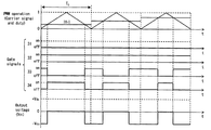
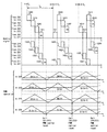
- FIGS. 3 and 4 are diagrams showing examples of PWM operation waveforms of the secondary side circuit 121 in the cell 101.
- FIG. FIG. 3 shows a PWM operation waveform when the voltage V 01 is controlled to a positive value. Specifically, as the PWM operation waveform, the carrier signal, the duty D 1 , the gate signal of the switching elements 31 to 34 and the V 01 waveform are shown. In addition, in FIG. 3, the dead time of the switching element is omitted for simplification of the drawings and the description.
- a triangular wave signal is shown as a carrier signal of PWM.
- the instantaneous value of the carrier signal changes in the range of 0 (0%) to 1 (100%).
- FIG. 3 shows PWM operation waveforms for three cycles of the carrier signal. In FIG. 3, the reset of the carrier signal described later is omitted.
- Duty D 1 is a control command for controlling the voltage V 01 to a desired value, is transmitted to the second control circuit 221 from the control signal transmitting unit 202 of the central controller 200 via the first control circuit 211 It is included in the control signal.
- Duty D 1 is a value from -1 (-100%) to +1 (+ 100%).
- the duty D 1 has a value from 0 to +1.
- Figure 3 between each period of the carrier signal, it was assumed that the duty D 1 is constant. Also, the case is shown where the duty D 1 gradually increases over three cycles of the carrier signal.
- switching elements 33 and 34 shown in FIG. 2 are controlled to be off and on, respectively.
- Switching elements 31 and 32 are on-off controlled according to the comparison result of the duty D 1 and the carrier signal. During the period the duty D 1 is greater than the carrier signal, the switching element 31 and 32 are controlled to turn on and off, (instantaneous value of) the voltage V 01 becomes + V dc. In duty D 1 is smaller period than the carrier signal, the switching element 31 and 32 are controlled to off and on, (instantaneous value of) V 01 becomes zero.
- the average value of the voltage V 01 in the carrier period is (D 1 V dc ). If the duty D 1 is changed in the range of 0 to +1, the inverter can output a desired voltage in the range of 0 ⁇ V 01 ⁇ + V dc as an average value in the carrier period. As in the example shown in FIG. 3, as the duty D 1 increases, the voltage V 01 (average value in the carrier period) also increases.
- FIG. 4 is a PWM operation waveform diagram in the case of controlling the voltage V 01 to a negative value.
- the duty D 1 takes a value from ⁇ 1 ( ⁇ 100%) to 0.
- showed
- the switching elements 31 and 32 are controlled to be off and on, respectively.
- the switching elements 33 and 34 are on / off controlled according to the comparison result of the absolute value
- the switching elements 33 and 34 are controlled to be on and off, respectively, and the voltage V 01 (the instantaneous value thereof) becomes ⁇ V dc .
- the switching elements 33 and 34 are controlled to be off and on, respectively, and the voltage V 01 (the instantaneous value thereof) becomes zero.
- the average value of the voltage V 01 in the carrier period is (D 1 V dc ).
- the utility D 1 is a negative value. If the duty D 1 is changed in the range of ⁇ 1 to 0, the inverter can output a desired voltage in the range of ⁇ V dc ⁇ V 01 ⁇ 0 as an average value in the carrier period. As in the example shown in FIG. 4, as
- the duty may be set to (V a / V dc ) with respect to the target value V dc of the DC link voltage.
- ⁇ V dc ⁇ V a ⁇ + V dc .
- control operation unit 201 generates target value V dc and duty (V a / V dc ) as control commands, and control signal transmission unit 202 generates a first control signal based on these control commands.
- Vdc is a fixed value and is recorded in both the central control unit 200 and the first control circuit 211.
- control operation unit 201 of the central control device 200 may also generate data (symbol) representing start or operation continuation of the converter as a control command. Also in the cells 102 to 104 (secondary circuits 122 to 124), the PWM processing is performed in the same manner.
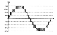
- FIG. 5 is a diagram showing an example of the combined output voltage V OS waveform. 5, the sine wave indicated by a broken line is a basic wave component contained in the combined output voltage V OS, may be considered as a target value of the combined output voltage V OS.
- the instantaneous value of the combined output voltage V OS is, -4V dc, -3V dc, ⁇ , 0, ⁇ , + 3V dc, made with any of the + 4V dc.
- power converter 1 as an average value in the carrier period, to output a desired voltage in the range of -4V dc ⁇ V OS ⁇ + 4V dc.
- FIG. 5 when the target value of the combined output voltage V OS is changed in a sinusoidal manner, a multi-level pseudo-sinusoidal combined output voltage V OS is generated.
- FIG. 6 is a timing chart showing the principle of PWM synchronization. Specifically, in FIG. 6, the synchronization signal waveform, the first control signal directed from the control signal transmission unit 202 of the central control unit 200 to the first control circuit 211 to 214 of each of the cells 101 to 104, each of the cells 101 to 104. Shows second control signals respectively transmitted from the first control circuits 211 to 214 to the second control circuits 221 to 224, and PWM operation waveforms performed in the second control circuits 221 to 224 of the respective cells 101 to 104. .
- the first control signal directed from the control signal transmission unit 202 of the central control device 200 to the first control circuit 211 is the first control circuit 211 among the first control signals transmitted from the control signal transmission unit 202. Means an address given.
- carrier signals generated by the second control circuits 221 to 224 and duties D 1 to D 4 are shown as PWM operation waveforms of the cells 101 to 104.
- Duty D 2 to D 4 is a control command for controlling V 02 to V 04 to a desired value, and from the control signal transmitting unit 202 of the central control unit 200 via the first control circuits 212 to 214, respectively. 2 included in the control signal transmitted to each of the control circuits 222 to 224.
- the specific values of the duties D 1 to D 4 in FIG. 6 are not values that are assumed to obtain the waveform of FIG. 5. Moreover, illustration is abbreviate
- T S represents a control cycle of central control unit 200. Specifically, it is a cycle in which the control operation unit 201 performs control operation and transmits the first control signal from the control signal transmission unit 202 to each of the cells 101 to 104.
- k is an integer representing a discrete time step.
- the control signal transmission unit 202 of the central control device 200 starts transmitting the first control signal to the first control circuits 211 to 214 of the cells 101 to 104.
- the control signal transmission unit 202 of the central control unit 200 The first control signal 1014 directed to the control circuit 214 is first transmitted.
- the first control signal 1013 directed to the first control circuit 213, the first control signal 1012 directed to the first control circuit 212, and the first control signal 1011 directed to the first control circuit 211 are sequentially transmitted.
- the control signal transmission unit 202 of the central control device 200 After transmitting the first control signal 1011 directed to the first control circuit 211, the control signal transmission unit 202 of the central control device 200 outputs a synchronization command to the synchronization signal transmission unit 203.
- the synchronization signal transmission unit 203 sets the synchronization signal, which is a digital signal, to H level in response to the reception of the synchronization command from the control signal transmission unit 202, and generates a rising edge of the synchronization signal.
- the rising of the synchronization signal occurs simultaneously with the completion of the transmission of the first control signal 1011, disregarding the processing delay during this period.
- the rising edge of the synchronization signal is output to the first control circuits 211 to 214 of all the cells 101 to 104.
- the first control circuits 211 to 214 of the cells 101 to 104 respectively transmit the second control signals 1021 to 1024 to the second control circuits 221 to 224 using the rising edge of the synchronization signal as a trigger. As mentioned above, these communications are simultaneously performed in all the cells 101 to 104.
- the second control signals 1021 to 1024 include information on the duties D 1 (k) to D 4 (k), respectively.
- the second control circuits 221 to 224 of each of the cells 101 to 104 use the reception of the second control signal as a trigger to reset the carrier signal.
- the value of the carrier signal generated by the second control circuit of each cell is initialized to 0 simultaneously with the completion of reception of the second control signal at time points t1, t2 and t3, and thereafter increases to 1 Begin (horizontal dashed line in FIG. 6 indicates "1").
- the reset of the carrier signal is also performed simultaneously for all the cells 101 to 104.
- the received D 1 (k) to D 4 (k) are reflected in the duty of each of the cells 101 to 104 after the reset.
- the cycle in which the rising of the synchronization signal occurs is T S as in the control cycle.
- Carrier period of each cell 101-104 is set to the same time as the control period T S of the central control unit 200.
- the carrier periods of the cells 101 to 104 do not have exactly the same time.
- the rising period T S of the synchronization signal does not have exactly the same value.
- the central control unit 200 and the second control circuits 221 to 224 perform computation, communication, PWM processing and the like by a digital control unit (microcomputer, digital signal processor, etc.).
- a digital control unit microcomputer, digital signal processor, etc.
- the carrier cycle of the second control circuit 221 is slightly shorter than T S
- the carrier cycle of the second control circuit 222 is slightly longer than T S of the central control unit 200.
- the carrier signals of the cells 101 to 104 can be substantially synchronized by simultaneously resetting the carrier signals of all the cells 101 to 104 as in the first embodiment. That is, as shown in FIG. 6, immediately before time t1, the carrier signals of the second control circuits 221 to 224 are gradually delayed as going from the second control circuits 221 to 224. For this reason, the carrier signals of the cells 101 to 104 can be substantially synchronized by simultaneously resetting the carrier signals of the second control circuits 221 to 224 at time t1.
- a cyclic error of the carrier signals of the second control circuits 221 to 224 occurs, but at time t2 by simultaneously resetting the carrier signals of the second control circuits 221 to 224.
- the carrier signals of the cells 101 to 104 can be approximately synchronized.
- the timing t3 is also similar to the timings t1 and t2.
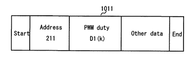
- FIG. 7 is a diagram showing a specific data configuration example of the first control signal 1011 shown in FIG.
- the first control signal 1011 is a serial communication signal of several bytes. Specifically, it comprises a start bit, an address portion, a duty portion, another data portion (Other data), and an end bit (stop bit).
- the address portion following the start bit is configured as digital data for identifying the first control circuit 211 of the cell 101.
- the duty part (PWM duty) is configured as digital data for indicating the value of the duty D 1 (k) shown in FIG.
- the other data portion (Other data) is constituted by digital data, parity bits or the like for indicating the contents of control commands other than duty. The existence and contents of other data parts can be set arbitrarily.
- FIG. 8 is a diagram showing a specific data configuration example of the second control signal 1021 shown in FIG.
- the second control signal 1021 is a serial communication signal of several bytes. Specifically, it comprises a start bit, a duty part (PWM duty), another data part, and an end bit (stop bit). Since the communication is performed inside the cell, the address part is unnecessary.
- the duty part is configured as digital data for indicating the value of the duty D 1 (k) shown in FIG. 6, and may have the same content as the duty part of the first control signal 1011 shown in FIG.
- the other data portion is composed of digital data for indicating the contents of control commands other than duty, or parity bits. The existence and contents of other data parts can be set arbitrarily.
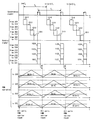
- FIG. 9 is a view showing a configuration example of the first control circuit 211 of the cell 101. As shown in FIG. The same configuration can be applied to the first control circuits 212 to 214 of the other cells 102 to 104.
- the first control circuit 211 includes a control signal reception unit 2111, a synchronization signal reception unit 2112, a control signal transmission unit 2113, and a drive control unit 2114.
- the control signal reception unit 2111 receives the first control signal transmitted from the control signal transmission unit 202 of the central control device 200, and confirms the address of the first control signal. When it is determined that the first control signal is directed to the first control circuit 211, the control command contained in the first control signal is extracted and the following processing is performed.
- a control command to the second control circuit 221 is output to the control signal transmission unit 2113 like a duty.
- a control command for the first converter 141 of the primary side circuit 111 is output to the drive control unit 2114.
- the synchronization signal reception unit 2112 detects the rising edge of the synchronization signal transmitted from the synchronization signal transmission unit 203 of the central control device 200, and outputs a transmission command to the control signal transmission unit 2113.
- the control signal transmission unit 2113 generates a second control signal based on the control command to the second control circuit 221 output by the control signal reception unit 2111. After that, it transmits to the second control circuit 221 according to the transmission command output from the synchronization signal reception unit 2112.
- the drive control unit 2114 drives and controls the first converter 141 in accordance with the control command on the first converter 141 output from the control signal receiving unit 2111.
- FIG. 10 is a diagram showing a configuration example of the second control circuit 221 of the cell 101. As shown in FIG. The same configuration as that of the second control circuit 221 can be applied to the second control circuits 222 to 224 of the other cells 102 to 104.
- the second control circuit 221 includes a control signal reception unit 2211, a carrier signal generation unit 2212, and a drive control unit 2213.
- the control signal receiving unit 2211 receives the second control signal transmitted from the first control circuit 211, extracts a duty that is a control command, and outputs the extracted duty to the drive control unit 2213. Further, the control signal receiving unit 2211 outputs a reset command to the carrier signal generating unit 2212 simultaneously with the completion of the reception of the second control signal.
- the carrier signal generation unit 2212 generates a carrier signal at a set carrier cycle, and outputs the carrier signal to the drive control unit 2213. Also, at the same time as receiving a reset command from the control signal receiving unit 2211, the carrier signal is reset.
- the drive control unit 2213 compares the duty from the signal reception unit 2211 with the carrier signal from the carrier signal generation unit 2212, and drives and controls the second converter 151 based on the result.
- FIG. 11 is a timing chart showing another example of PWM synchronization. Only the difference from the PWM synchronization described in FIG. 6 will be described below.
- the configuration shown in FIG. 11 for resetting the carrier signal after a predetermined time T W has passed since the second control circuits 221 to 224 have received the second control signal is different from all the embodiments described below. It can be applied as
- the duty is transmitted from the central control unit 200 to the second control circuits 221 to 224 and the second control circuits 221 to 224 independently perform the PWM processing.
- the primary side circuits 111 to 114 of the cells 101 to 104 are connected in parallel to the external power supply 300, and the ground potentials of the first control circuits 211 to 214 are all common.
- the ground potentials of the central control unit 200 and the first control circuits 211 to 214 can also be shared. Therefore, for communication from the central control unit 200 to the first control circuits 211 to 214, insulation is not necessary, communication using an electric wire can be applied, and the cost for insulation processing can be omitted.
- the power conversion apparatus when used for an inverter for driving a high voltage motor or PCS for a high voltage distribution system, a withstand voltage exceeding 5 kV is required unless the first embodiment of the present invention is applied. It is expensive.
- a low cost power converter that performs PWM synchronization can be realized.
- FIG. 12 is a timing chart showing the principle of PWM synchronization in the second embodiment.
- the configuration of the power conversion device in the second embodiment is the same as the configuration of the first embodiment shown in FIG. 1, and therefore the illustration and the detailed description will be omitted.
- the second control signal transmitted to each of the control circuits 221 to 224 includes information of a reset command in addition to the duty as a control command.
- the reset command is a 1-bit control command which is information indicating whether the second control circuits 221 to 224 reset the carrier signal after receiving the control signal (on or off).
- the first control circuit 211 directed from the control signal transmission unit 202 of the central control unit 200 to the first control circuit 211
- the reset command of the first control signal 1311 is turned on as described above.
- the first control circuit 211 of the cell 101 After receiving the first control signal 1311, the first control circuit 211 of the cell 101 transmits a second control signal 1321 to the second control circuit 221 using the rising edge of the synchronization signal as a trigger. At this time, in response to the reset command of the first control signal 1311 being on, the reset command of the second control signal 1321 is also turned on.
- the second control circuit 221 resets the carrier signal using the reception of the second control signal 1321 as a trigger in response to the reset command of the second control signal 1321 being on.
- the first control signal 1411 directed from the control signal transmitting unit 202 of the central controller 200 to the first control circuit 211 does not turn on the reset command (Although illustration is omitted, the reset command is set to off). Therefore, the reset command is also set to OFF for the second control signal 1421 from the first control circuit 211 to the second control circuit 221.
- the second control circuit 221 In response to the reset instruction of the second control signal 1421 being off, the second control circuit 221 does not reset the carrier signal even if the second control signal 1421 is received.
- the second embodiment is slightly different from the first embodiment in the configuration and operation of the first control circuits 211 to 214 and the second control circuits 221 to 224. However, since the operation has been described above, FIG. The illustration of a block diagram such as 10 is omitted.
- the carrier signal is reset in every control cycle, but as in the second embodiment, the carrier cycle of each of the cells 101 to 104 and the control cycle T S of the central control unit 200 Is sufficiently small, the carrier signals of each cell can be substantially synchronized even if the carrier signals are not reset in all control cycles.
- the second embodiment is applicable to one in which the operation level of the control unit such as a microcomputer is lower than that of the first embodiment.
- the control unit such as a microcomputer
- FIG. 13 is a timing chart showing the principle of PWM synchronization in the third embodiment.
- the configuration of the power conversion device according to the third embodiment is the same as the configuration of the first embodiment shown in FIG. 1 and thus the illustration and the detailed description will be omitted.
- the control signal transmission unit 202 of the central control device 200 transmits only the first control signal 1114 directed to the first control circuit 214 and the first control signal 1113 directed to the first control circuit 213 in order.
- the central control device 200 completes the calculation of the duty by communicating the control signal and resetting the carrier signal as shown in FIG.
- the time until the duty is reflected in the second control circuit, that is, the delay time by communication can be shortened.
- FIG. 14 is a schematic configuration diagram of a power conversion device in a fourth embodiment. Hereinafter, only differences from the power conversion device 1 in the first embodiment described with reference to FIG. 1 will be described.
- the power conversion device 2 shown in FIG. 14 includes a central control unit 204 instead of the central control unit 200 of FIG.
- the central control unit 204 of FIG. 14 does not include the synchronization signal transmission unit 203 as compared with the central control unit 200 of the first embodiment, and the synchronization control signal is sent to the first control circuits 211 to 214 of 101 to 104 of each cell. It is configured not to output.
- FIG. 15 is a timing chart showing the principle of PWM synchronization in the fourth embodiment.
- the control signal includes a reset command.
- the difference from the PWM synchronization in the second embodiment described with reference to FIG. 12 will be described.
- control signal transmission unit 202 of the central control unit 204 transmits the first control signal directed to the first control circuits 211 to 214 at each control cycle.
- the control signal transmission unit 202 performs the output of the first control signal four times (for four frames) per control cycle, but the first control signal of the fourth in time (the first control signals 1311, 1412 and 1513 in FIG. 15) Set the reset command to on for.
- the address in the fourth first control signal is rotated among the first control circuits 211 to 214 of the cells 101 to 104.
- the address in the fourth control signal changes to the cell 101 (first control circuit 211), the cell 102 (first control circuit 212), and the cell 103 (first control circuit 213).
- the first control circuits 211 to 214 of each of the cells 101 to 104 receive the first control signal transmitted by the control signal transmission unit 202 of the central control device 200, and immediately receive the second control signal to the second control circuits 221 to 224. Send After receiving the second control signal, the second control circuits 221 to 224 of each of the cells 101 to 104 reset the carrier signal if the reset command is on.
- the time from the starting point of the control cycle (the time when communication of the first control signal by the control signal transmission unit 202 starts) to the reset of the carrier signal can be kept constant, as shown in FIG. realizable.
- the configuration of the central control unit 204 and the wiring from the central control unit 204 to each of the cells 101 to 104 can be simplified as much as the synchronization signal is not used.
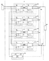
- FIG. 16 is a schematic configuration diagram of a power conversion device in a fifth embodiment of the present invention.
- the power conversion device 3 of FIG. 16 includes four cells 105 to 108.
- the difference between the first embodiment and the fifth embodiment shown in FIG. 1 is that the input terminals (input sides) of the cells 105 to 108 are connected in series, and the combined input terminal is connected to the external power supply 301.
- the output terminals (output side) of the cells 105 to 108 are connected in parallel to the load 401.
- the cells 105 to 108 include primary circuits 115 to 118, secondary circuits 125 to 128, and transformers 135 to 138, respectively.
- the primary side circuits 115 to 118 include second converters 155 to 158 and second control circuits 225 to 228 for controlling them, and the secondary side circuits 125 to 128 include first converters 145 to 148 and The first control circuits 215 to 218 that control these are provided, respectively, and the internal configuration of the cells 105 to 108 is the same as that of the cells 101 to 104 of the first embodiment, so The PWM synchronization can be applied to the fifth embodiment as it is.
- the configuration of the fifth embodiment can be applied to a power converter that converts the primary side to a high voltage of, for example, 66 kv and converts the secondary side to a low voltage of, for example, 100 v.
- Sixth Embodiment A sixth embodiment of the present invention is an example in which three power conversion devices 1 described in the first embodiment are used to configure a three-phase AC power conversion device.
- FIG. 17 is a schematic configuration diagram of the power conversion device 4 in the sixth embodiment.
- the power conversion device 4 shown in FIG. 17 includes three power conversion devices 1 described in the first embodiment.
- one of the output terminals provided in the three power electronics devices 1 constitutes a three-phase output terminal, and is connected to the three-phase load 401.
- the other (one other) of the output terminals provided in the three power electronics devices 1 are connected to one another to form a neutral point in the Y-connected three-phase AC circuit.
- the input terminals of the three power electronics devices 1 are connected in parallel to each other and connected to the power supply 300.
- the power conversion device 1 includes the central control device 200 therein. Therefore, although the power conversion device 4 of FIG. 17 is provided with three central control devices 200, the three central control devices 200 may be integrated into one.
- the sixth embodiment of the present invention can be applied to, for example, an inverter for driving a three-phase high voltage motor or a three-phase AC power system PCS, and is also an embodiment of a power converter outputting three-phase AC. An effect similar to 1 can be obtained.
- the plurality of cells 101 to 104 are connected in parallel to the external power supply 300 and connected in series to the external load 400
- the fifth embodiment includes the plurality of cells 105.
- 108 to 108 are connected in series to the external power supply 301 and in parallel to the load 401
- a plurality of cells are connected in series to the external power supply and are also connected in series to the load. Even if there are, the present invention is applicable.
Abstract
The present invention achieves a low-cost power conversion device that performs PWM synchronization. This power conversion device is provided with power conversion cells 101-104 that supply the voltage of a power supply 300 to a load 400, and a central control unit 200 that controls these power conversion cells. The power conversion cells 101-104 respectively comprise first converters 141-144 and first control circuits 211-214 for respectively controlling these first converters, second converters 151-154 and second control circuits 221-224 for respectively controlling these second converters by pulse width modulation, and transformers 131-134 respectively connected between the first converters 141-144 and the second converters 151-154. The central control unit 200 transmits a first control signal and a synchronization signal to the first control circuits 211-214 of the power conversion cells 101-104, the first control circuits 211-214 transmit a second control signal to the second control circuits 221-224 of the power conversion cells 101-104 upon receipt of the synchronization signal, and the second control circuits 221-224 reset a carrier signal for the pulse width modulation upon receipt of the second control signal.
Description
本発明は電力変換装置に関する。
The present invention relates to a power converter.
高電圧または大容量の電力変換においては、複数の電力変換セル(以下、セルと略す)を直列または並列に接続した電力変換装置が用いられる。このような電力変換装置として、特許文献1に記載された多重電力変換器がある。この多重電力変換器では、複数台のインバータユニット(セルに相当)の出力をそれぞれ直列に接続して高圧出力を得ている。
In high-voltage or large-capacity power conversion, a power conversion device in which a plurality of power conversion cells (hereinafter referred to as cells) are connected in series or in parallel is used. As such a power converter, there is a multiple power converter described in Patent Document 1. In this multiplex power converter, outputs of a plurality of inverter units (corresponding to cells) are respectively connected in series to obtain a high voltage output.
特許文献1には、複数のインバータユニットのPWM(Pulse Width Modulation:パルス幅変調)について記載されている。
Patent Document 1 describes PWM (Pulse Width Modulation) of a plurality of inverter units.
具体的には、インバータユニットの台数に応じた複数の搬送波(キャリア)信号を利用して、各インバータユニットが備える半導体素子(スイッチング素子)のオン・オフ状態を制御する。これによって、多段(マルチレベル)の出力電圧が得られる。
Specifically, the on / off state of the semiconductor element (switching element) included in each inverter unit is controlled by using a plurality of carrier waves according to the number of inverter units. Thus, multistage (multilevel) output voltages can be obtained.
特許文献1に記載されているように、複数のキャリア信号はそれぞれ同位相になっている。複数のキャリア信号の位相を同期させることは、出力電圧に含まれる高調波成分を抑制する上で有効と考えられる。また、出力電圧が一度に複数レベル変化して、モータなどの負荷に悪影響を及ぼすことを抑制する上でも有効と考えられる。
As described in Patent Document 1, a plurality of carrier signals are in phase with one another. Synchronizing the phases of a plurality of carrier signals is considered to be effective in suppressing harmonic components included in the output voltage. Moreover, it is considered effective also in suppressing that the output voltage changes a plurality of levels at once and adversely affecting the load such as a motor.
このような電力変換装置の構成は、高電圧モータを直接駆動する場合に有効である。
Such a configuration of the power conversion device is effective when directly driving a high voltage motor.
また、太陽光発電や風力発電といった自然エネルギー発電の導入が世界的に拡大しているが、自然エネルギーから得られる電力を変換して電力系統に出力するための電力変換装置としてPCS(パワーコンディショニングシステム)がある。PCSの高電圧化や大容量化においても、複数のセルを用いる構成が有効と考えられる。
In addition, although the introduction of natural energy generation such as solar power generation and wind power generation is expanding worldwide, PCS (power conditioning system) is used as a power conversion device to convert electric power obtained from natural energy and output it to the electric power system. ). A configuration using a plurality of cells is considered to be effective also in increasing the voltage and increasing the capacity of the PCS.
ここで、以下の説明においては、複数セルのPWMに利用される複数のキャリア信号について、位相を同期させることをPWM同期と定義する。
Here, in the following description, synchronization of phases of a plurality of carrier signals used for PWM of a plurality of cells is defined as PWM synchronization.
PWM同期の実現には、以下の課題があると考えられる。
The realization of PWM synchronization is considered to have the following problems.
複数セルを統括制御するために中央制御装置を設ける場合、中央制御装置が全セルのPWM処理を行い、生成されたスイッチング素子のゲート信号を各セルの制御回路まで伝送する構成が考えられる。
When a central control unit is provided to integrally control a plurality of cells, a configuration is conceivable in which the central control unit performs PWM processing of all the cells and transmits the generated gate signal of the switching element to the control circuit of each cell.
しかし、セルが備えるスイッチング素子は1個ではなく複数であることが多いため、スイッチング素子の数に応じて複数のゲート信号配線を施すことになり、電力変換装置の複雑化、高コスト化が問題となる。
However, since a cell often includes a plurality of switching elements instead of one, a plurality of gate signal lines are provided according to the number of switching elements, which causes a problem of the complexity and cost increase of the power conversion device. It becomes.
本発明の目的は、PWM同期を行う低コストの電力変換装置を実現することである。
An object of the present invention is to realize a low cost power converter that performs PWM synchronization.
上記目的を達成するため、本発明は次のように構成される。
In order to achieve the above object, the present invention is configured as follows.
電力変換装置において、電源電圧を負荷に供給する電圧に変換する複数の電力変換セルと、上記複数の電力変換セルを制御する中央制御装置と、を備え、上記複数の電力変換セルのそれぞれは、上記電源電圧を変換する第1変換器と、この第1変換器を制御する第1制御回路と、上記第1変換器により変換された電圧を変換する第2変換器と、この第2変換器をパルス幅変調によって制御する第2制御回路と、上記第1変換器と上記第2変換器の間に接続されるトランスとを有し、
上記中央制御装置は、上記複数の電力変換セルのそれぞれが有する上記第1制御回路に第1制御信号を送信する制御信号送信部を有し、上記第1制御信号に基づいて、上記複数の電力変換セルのそれぞれが有する第1制御回路が上記第1変換器を制御し、上記第2制御回路が上記第2変換器を制御し、上記パルス幅変調のキャリア信号をリセットする。 The power converter includes: a plurality of power conversion cells for converting a power supply voltage into a voltage for supplying a load; and a central control unit for controlling the plurality of power conversion cells, each of the plurality of power conversion cells being A first converter for converting the power supply voltage, a first control circuit for controlling the first converter, a second converter for converting the voltage converted by the first converter, and a second converter A second control circuit for controlling the pulse width modulation by pulse width modulation, and a transformer connected between the first converter and the second converter,
The central control device includes a control signal transmission unit that transmits a first control signal to the first control circuit included in each of the plurality of power conversion cells, and based on the first control signal, the plurality of powers A first control circuit included in each of the conversion cells controls the first converter, and the second control circuit controls the second converter to reset the carrier signal of the pulse width modulation.
本発明によれば、PWM同期を行う低コストの電力変換装置を実現することができる。
According to the present invention, a low cost power converter that performs PWM synchronization can be realized.
以下、本発明の実施形態について、添付図面を参照して詳細に説明する。
Hereinafter, embodiments of the present invention will be described in detail with reference to the attached drawings.
(実施例1)
図1は、本発明の実施例1における電力変換装置の概略構成図である。 Example 1
FIG. 1 is a schematic configuration diagram of a power conversion device according to a first embodiment of the present invention.
図1は、本発明の実施例1における電力変換装置の概略構成図である。 Example 1
FIG. 1 is a schematic configuration diagram of a power conversion device according to a first embodiment of the present invention.
図1において、電力変換装置1は、外部の電源300から入力される電力を変換し、外部の負荷400に出力する。また、電力変換装置1は、複数のセル101~104とこれらを制御する中央制御装置200を備える。図1では、セルを4台利用する例を示したが、台数については任意である。
In FIG. 1, the power conversion device 1 converts power input from an external power supply 300 and outputs the converted power to an external load 400. Further, the power conversion device 1 includes a plurality of cells 101 to 104 and a central control device 200 that controls them. Although FIG. 1 shows an example in which four cells are used, the number is arbitrary.
セル101~104は、第1変換器141~144及びこれらを制御する第1制御回路211~214と、第2変換器151~154及びこれらを制御する第2制御回路221~224と、第1変換器141~144と第2変換器151~154の間にそれぞれ接続されるトランス131~134をそれぞれ備える。
The cells 101 to 104 include first converters 141 to 144 and first control circuits 211 to 214 for controlling them, second converters 151 to 154, second control circuits 221 to 224 for controlling them, and Transformers 131 to 134 connected respectively between the converters 141 to 144 and the second converters 151 to 154 are provided.
以下では、第1変換器141~144と第1制御回路211~214を合わせて1次側回路111~114とそれぞれ定義する。また、第2変換器151~154と第2制御回路221~224を合わせて2次側回路121~124とそれぞれ定義する。トランス131~134は、1次側回路111~114と2次側回路121~124をそれぞれ電気的に絶縁する。セルのさらに詳細な構成については、後述する。
Hereinafter, the first converters 141 to 144 and the first control circuits 211 to 214 are collectively defined as primary circuits 111 to 114, respectively. The second converters 151 to 154 and the second control circuits 221 to 224 are collectively defined as secondary circuits 121 to 124, respectively. The transformers 131 to 134 electrically insulate the primary side circuits 111 to 114 and the secondary side circuits 121 to 124, respectively. A more detailed configuration of the cell will be described later.
セル101~104の入力端子(入力側)は、電源300に対して並列に接続される。従って、セル101~104の入力電圧は全て等しい。セル101~104は、電源300の電圧を変換して出力電圧VO1~VO4をそれぞれ生成する。
The input terminals (input sides) of the cells 101 to 104 are connected in parallel to the power supply 300. Therefore, the input voltages of the cells 101 to 104 are all equal. The cells 101 to 104 convert the voltage of the power supply 300 to generate output voltages V O1 to V O4 , respectively.
セル101が出力電圧VO1を生成する要領を説明する。
The manner in which the cell 101 generates the output voltage V O1 will be described.
まず、1次側回路111の第1変換器141は、電源300の電圧を交流電圧に変換してトランス131の1次巻線に印加する。1次側回路111の第1制御回路211は、この動作に関する演算・処理を行い、第1変換器141を駆動する。
First, the first converter 141 of the primary side circuit 111 converts the voltage of the power supply 300 into an alternating voltage and applies it to the primary winding of the transformer 131. The first control circuit 211 of the primary side circuit 111 performs calculation and processing related to this operation to drive the first converter 141.
次に、2次側回路121の第2変換器151は、トランス131の2次巻線に発生する電圧を変換して電圧VO1を生成する。2次側回路121の第2制御回路221は、この動作に関する演算・処理を行い、第2変換器151を駆動する。セル102~104についても、同様の要領で電圧VO2~VO4をそれぞれ生成する。
Next, the second converter 151 of the secondary side circuit 121 converts the voltage generated in the secondary winding of the transformer 131 to generate the voltage V O1 . The second control circuit 221 of the secondary side circuit 121 performs operation and processing related to this operation to drive the second converter 151. Also for cells 102 to 104, voltages V O2 to V O4 are respectively generated in the same manner.
セル101~104の出力端子(出力側)は、互いに直列に接続される。電力変換装置1の出力電圧は、電圧VO1~VO4を合成した電圧であり、以下では、これを合成出力電圧VOS(=VO1+VO2+VO3+VO4)と定義する。以上の構成によって、電力変換装置1は各セルの定格出力電圧より高い電圧を出力できる。
The output terminals (output side) of the cells 101 to 104 are connected in series with one another. The output voltage of the power conversion device 1 is a voltage obtained by combining the voltages V O1 to V O4 . Hereinafter, this is defined as a combined output voltage V OS (= V O1 + V O2 + V O3 + V O4 ). With the above configuration, the power conversion device 1 can output a voltage higher than the rated output voltage of each cell.
ここで、2次側回路121~124は、後述のようにPWM(パルス幅変調)を利用して出力電圧VO1~VO4をそれぞれ制御する。第2制御回路221は、内部で生成するキャリア信号と、外部から送信されるデューティ比(以下、デューティと略称する)を用いてPWM処理を行い、その結果に従って第2変換器151を駆動する。デューティとは、PWMにおいてスイッチング素子のオン期間比率を設定するための数値である。デューティは、電圧VO1を所望の値に制御するために中央制御装置200によって生成される。
Here, the secondary side circuits 121 to 124 respectively control the output voltages V O1 to V O4 using PWM (Pulse Width Modulation) as described later. The second control circuit 221 performs PWM processing using a carrier signal generated internally and a duty ratio (hereinafter abbreviated as duty) transmitted from the outside, and drives the second converter 151 according to the result. The duty is a numerical value for setting the on period ratio of the switching element in PWM. The duty is generated by central controller 200 to control voltage V O1 to a desired value.
第2制御回路222~224も同様にPWM処理を行い、第2変換器152~154をそれぞれ駆動する。第2制御回路221~224によるキャリア信号生成は独立しているが、後述の方法によってPWM同期が実現される。
The second control circuits 222 to 224 similarly perform PWM processing to drive the second converters 152 to 154, respectively. Although carrier signal generation by the second control circuits 221 to 224 is independent, PWM synchronization is realized by the method described later.
ここで、本発明とは異なる例であるが、2次側回路121~124のPWMにおいては、中央制御装置200が2次側回路121~124のPWM処理を全て行い、生成されたスイッチング素子のゲート信号を2次側回路121~124まで伝送する構成も考えられる。
Here, although this is an example different from the present invention, in the PWM of the secondary side circuits 121 to 124, the central control unit 200 performs all the PWM processing of the secondary side circuits 121 to 124, and A configuration in which the gate signal is transmitted to the secondary side circuits 121 to 124 is also conceivable.
しかし、後述のように第2変換器のスイッチング素子は複数個あるため、その分だけ複数のゲート信号配線が必要になり、電力変換装置の複雑化、高コスト化が問題となる。
However, as described later, since there are a plurality of switching elements of the second converter, a plurality of gate signal lines are required accordingly, and the power converter becomes complicated and expensive.
一方、本発明の実施例1のように、中央制御装置200から第2制御回路221~224にデューティを送信し、第2制御回路221~224が独立してPWM処理を実施する構成であれば、中央制御装置200から各セルへの制御信号に関する配線の複雑化、高コスト化を抑制することができる。
On the other hand, as in the first embodiment of the present invention, if the central control unit 200 transmits the duty to the second control circuits 221 to 224 and the second control circuits 221 to 224 independently perform the PWM processing. It is possible to suppress the increase in complexity and cost of wiring relating to the control signal from central controller 200 to each cell.
中央制御装置200は、合成出力電圧VOSを所望の値に制御するために、各セル101~104の出力電圧VO1~VO4を制御する。
The central control unit 200 controls the output voltages V O1 to V O4 of the cells 101 to 104 in order to control the combined output voltage V OS to a desired value.
電力変換装置1を太陽光発電のPCSに応用する場合、電力変換装置1の出力電流を所望の値に制御することが要求される。図1では、このような場合を想定して、出力電流の経路上に電流検出器230を配置している。
When applying the power conversion device 1 to a PCS of solar power generation, it is required to control the output current of the power conversion device 1 to a desired value. In FIG. 1, assuming such a case, the current detector 230 is disposed on the path of the output current.
中央制御装置200が備える制御演算部201は、電流検出器230から検出される出力電流の検出値を用いてフィードバック制御の演算を行い、出力電圧VOSの目標値、ひいては各出力セル101~104の電圧VO1~VO4の目標値を生成する。
The control calculation unit 201 included in the central control unit 200 performs calculation of feedback control using the detected value of the output current detected from the current detector 230, and calculates the target value of the output voltage V OS and thus each output cell 101 to 104. Target values of voltages V O1 to V O4 are generated.
さらに、制御演算部201は、電圧VO1~VO4を目標値とするための演算・処理を行い、各セル101~104の第1制御回路211~214と第2制御回路221~224とに対して制御指令を生成する。制御指令とは、制御の目標値(指令値)、または、起動や停止などの状態指示であり、前述のデューティも制御指令に含まれる。
Furthermore, the control calculation unit 201 performs calculation and processing for setting the voltages V O1 to V O4 as target values, and the first control circuits 211 to 214 and the second control circuits 221 to 224 of the respective cells 101 to 104 Generate control commands. The control command is a target value (command value) of control or a state command such as start or stop, and the above-described duty is also included in the control command.
制御演算部201は、生成した制御指令を制御信号送信部202に出力する。図1では、4台のセル101~104ごとに個別の制御指令を出力することを表すために、制御指令として4本の矢印を示した。制御信号送信部202は、制御指令に基づいて各セル101~104に対する第1制御信号を生成し、各セル1101~104の第1制御回路211~214に第1制御信号を送信する。
The control operation unit 201 outputs the generated control command to the control signal transmission unit 202. In FIG. 1, four arrows are shown as control commands in order to indicate that individual control commands are output for each of the four cells 101 to 104. The control signal transmission unit 202 generates a first control signal for each of the cells 101 to 104 based on the control command, and transmits the first control signal to the first control circuit 211 to 214 of each of the cells 1101 to 104.
制御信号送信部202が送信する第1制御信号には、デューティのように第2制御回路221~224に対する制御指令が含まれる。このように第2制御回路221~224に向けた制御指令であっても、一旦、第2制御回路221~224が属するセル101~104の第1制御回路211~214に送信する。
The first control signal transmitted by the control signal transmission unit 202 includes a control instruction to the second control circuits 221 to 224 like a duty. As described above, even the control command directed to the second control circuits 221 to 224 is temporarily transmitted to the first control circuits 211 to 214 of the cells 101 to 104 to which the second control circuits 221 to 224 belong.
すなわち、第1制御回路211~214を用いた中継を行い、制御指令を第2制御回路221~224に送信する。
That is, relay is performed using the first control circuits 211 to 214, and a control command is transmitted to the second control circuits 221 to 224.
各セル101~104の1次側回路111~114は、外部電源300に対して並列に接続される。そのため、第1制御回路211~214のグラウンド電位(回路が動作する基準電位)は全て共通である。また、中央制御装置200と第1制御回路211~214のグラウンド電位も共通化できる。よって、中央制御装置200から第1制御回路211~214への通信については、絶縁は不要であり、電線を用いた通信を適用できる。
The primary side circuits 111 to 114 of the cells 101 to 104 are connected in parallel to the external power supply 300. Therefore, the ground potentials of the first control circuits 211 to 214 (reference potentials at which the circuits operate) are all common. Further, the ground potentials of the central control unit 200 and the first control circuits 211 to 214 can be shared. Therefore, for communication from the central control unit 200 to the first control circuits 211 to 214, insulation is not necessary, and communication using electric wires can be applied.
本実施例1では、中央制御装置200の制御信号送信部202から第1制御回路211~214への通信方法として、シリアル通信を想定する。そのため、第1制御信号は数バイト程度のシリアル通信信号となる。
In the first embodiment, serial communication is assumed as a communication method from the control signal transmission unit 202 of the central control device 200 to the first control circuits 211 to 214. Therefore, the first control signal is a serial communication signal of several bytes.
また、本実施例1では、中央制御装置200の制御信号送信部202と全ての第1制御回路211~214との間で通信バスを共有し、この通信バスにより、制御信号送信部202と全ての第1制御回路211~214とが接続される。そのため、図1では、制御信号送信部202から出力される第1制御信号として、1本の矢印を示し、それを各セルの第1制御回路211~214に並列に入力する構成を示した。後述のように、第1制御信号は、セル101~104を識別するためのアドレスを含む。このため、制御信号送信部202は、制御指令を符号化し、さらにアドレスを付与してシリアル通信信号を生成する。
Further, in the first embodiment, a communication bus is shared between the control signal transmission unit 202 of the central control device 200 and all the first control circuits 211 to 214, and all of the control signal transmission unit 202 is shared by this communication bus. And the first control circuits 211 to 214 are connected. Therefore, FIG. 1 shows one arrow as the first control signal output from the control signal transmission unit 202, and shows a configuration in which it is input in parallel to the first control circuits 211 to 214 of each cell. As described later, the first control signal includes an address for identifying the cells 101 to 104. For this reason, the control signal transmission unit 202 encodes the control command and further adds an address to generate a serial communication signal.
中央制御装置200において、制御信号送信部202は、同期信号送信部203に対して同期指令を出力する。同期信号送信部203は、同期信号送信部202から出力された同期指令に基づいて同期信号を生成し、第1制御回路211~214に出力する。第1制御回路211~214に出力される同期信号は、PWM同期に利用されるディジタル信号であり、詳細については後述する。
In central control unit 200, control signal transmission unit 202 outputs a synchronization instruction to synchronization signal transmission unit 203. The synchronization signal transmission unit 203 generates a synchronization signal based on the synchronization command output from the synchronization signal transmission unit 202, and outputs the synchronization signal to the first control circuits 211 to 214. The synchronization signals output to the first control circuits 211 to 214 are digital signals used for PWM synchronization, and the details will be described later.
中央制御装置200の同期信号送信部203から第1制御回路211~214への同期信号の伝送においても、グランド電位を共通化できるため、絶縁は不要であり、電線を用いた信号伝送を適用できる。
Also in transmission of synchronization signals from the synchronization signal transmission unit 203 of the central control unit 200 to the first control circuits 211 to 214, since the ground potential can be shared, insulation is not necessary, and signal transmission using electric wires can be applied. .
本実施例1では、中央制御装置200の同期信号送信部203から全ての第1制御回路211~214に対して共通の同期信号を出力する。図1では、同期信号送信部203から出力される同期信号として1本の矢印を示し、それを第1制御回路211~214に並列に入力する構成を示した。
In the first embodiment, the synchronization signal transmission unit 203 of the central control device 200 outputs a common synchronization signal to all of the first control circuits 211 to 214. In FIG. 1, one arrow is shown as the synchronization signal output from the synchronization signal transmission unit 203, and the configuration to input it in parallel to the first control circuits 211 to 214 is shown.
本発明の実施例1とは異なる例であり、中央制御装置200から各セル101~104への信号伝送において絶縁が必要となる場合、高価な光ファイバを利用する方法が考えられる。その場合、中央制御装置200から各セルへの配線は長距離になり得るため、使用する光ファイバの合計長が長くなり、電力変換装置のコストが高くなる。
This is an example different from the first embodiment of the present invention, and when the signal transmission from the central control unit 200 to each of the cells 101 to 104 requires insulation, a method using an expensive optical fiber can be considered. In that case, since the wiring from the central control unit 200 to each cell can be a long distance, the total length of optical fibers to be used becomes long, and the cost of the power converter becomes high.
一方、本実施例1では、グランド電位を共通化することがきるため、中央制御装置200から各セル101~104に対する全ての信号伝送について絶縁が不要であり、高価な光ファイバではなく、安価な電線を使用できるため、低コストの電力変換装置を実現できる。
On the other hand, in the first embodiment, since the ground potential can be made common, insulation is not necessary for all signal transmission from the central control unit 200 to each of the cells 101 to 104, which is not expensive optical fiber but inexpensive. Since electric wires can be used, a low cost power converter can be realized.
さらに、図1のように全セル101~104で通信バスを共通化すれば、中央制御装置200の出力ポート数が減少し、より低コストの電力変換装置を実現できる。また、配線の煩雑化を抑える点でもメリットがある。
Furthermore, as shown in FIG. 1, if the communication buses are shared among all the cells 101 to 104, the number of output ports of central control apparatus 200 can be reduced, and a lower cost power converter can be realized. There is also an advantage in terms of suppressing the complexity of the wiring.
第1制御回路211は、受信した第1制御信号から第1変換器141に関する制御指令を抽出し、これに従って第1変換器141を駆動する。また、第1制御回路211は、第1制御信号から第2変換器151に関する制御指令(デューティなど)を抽出し、抽出した制御指令に基づいて第2制御信号を生成し、生成した第2制御信号を第2制御回路221に送信する。第1制御回路211から第2制御回路221への通信は、中央制御装置200の同期信号送信部203から送信される同期信号の立ち上がり(または立ち下がり)をトリガとして行われる。
The first control circuit 211 extracts a control command related to the first converter 141 from the received first control signal, and drives the first converter 141 accordingly. Further, the first control circuit 211 extracts a control command (such as a duty) for the second converter 151 from the first control signal, generates a second control signal based on the extracted control command, and generates a second control generated. A signal is sent to the second control circuit 221. Communication from the first control circuit 211 to the second control circuit 221 is triggered by the rise (or fall) of the synchronization signal transmitted from the synchronization signal transmission unit 203 of the central control device 200.
第1制御回路212~214についても、上述した第1制御回路211と同様の要領で第1変換器142~144をそれぞれ駆動し、第2制御回路222~224に第2制御信号をそれぞれ送信する。
The first control circuits 212 to 214 also drive the first converters 142 to 144 in the same manner as the above-described first control circuit 211, and transmit the second control signals to the second control circuits 222 to 224, respectively. .
ここで、中央制御装置200の同期信号送信部203から全セル101~104の第1制御回路211~214に対して共通の同期信号を出力するため、第1制御回路211~214から第2制御回路221~224への通信は全セル101~104で同時に行われる。後述するように、各セル101~104の第2制御回路221~224は、第2制御信号の受信をトリガとしてキャリア信号をリセットする。以上によって、PWM同期を実現できる。
Here, in order to output a common synchronization signal from the synchronization signal transmission unit 203 of the central control unit 200 to the first control circuits 211 to 214 of all the cells 101 to 104, the first control circuits 211 to 214 perform second control. Communication to circuits 221-224 is simultaneously performed in all cells 101-104. As described later, the second control circuits 221 to 224 of each of the cells 101 to 104 use the reception of the second control signal as a trigger to reset the carrier signal. Thus, PWM synchronization can be realized.
本実施例1では、各セル101~104の第1制御回路211~214から第2制御回路221~224への通信手段として、シリアル通信を利用する。そのため、第2制御信号は数バイト程度のシリアル通信信号となる。
In the first embodiment, serial communication is used as communication means from the first control circuits 211 to 214 of the cells 101 to 104 to the second control circuits 221 to 224. Therefore, the second control signal is a serial communication signal of several bytes.
各セル101~104の2次側回路121~124は、互いに直列に接続されるため、第2制御回路221~224のグラウンド電位はそれぞれ異なる。また、第1制御回路211~214と第2制御回路221~224のグラウンド電位もそれぞれ異なる。このため、各セル101~104の第1制御回路211~214から第2制御回路221~224への通信には絶縁が必要である。よって、例えば、光ファイバを利用した通信が考えられる。ただし、セル101~104の内部の通信となるため、光ファイバの合計長は比較的短くなり、光ファイバのコストを低く抑えられる。
Since the secondary side circuits 121 to 124 of the cells 101 to 104 are connected in series with each other, the ground potentials of the second control circuits 221 to 224 are different from each other. In addition, the ground potentials of the first control circuits 211 to 214 and the second control circuits 221 to 224 are also different. Therefore, the communication from the first control circuits 211 to 214 of the cells 101 to 104 to the second control circuits 221 to 224 requires insulation. Therefore, for example, communication using an optical fiber can be considered. However, since the communication is performed inside the cells 101 to 104, the total length of the optical fibers becomes relatively short, and the cost of the optical fibers can be reduced.
また、各セル101~104の第1制御回路211~214から第2制御回路221~224への通信は比較的短距離となることから、光ファイバの他に、IrDA(Infrared Data Association)のような赤外線通信や超音波等を利用する方法も考えられる。赤外線通信や超音波通信であれば、第1制御回路211~214と第2制御回路221~224とでグラウンド電位が大きく異なる場合であっても、赤外線通信や超音波通信の送受信機の距離を適切に保つなど構造上の工夫によって絶縁を確保しつつ通信することができる。
Further, since communication from the first control circuits 211 to 214 to the second control circuits 221 to 224 in each of the cells 101 to 104 is a relatively short distance, in addition to the optical fiber, it may be similar to IrDA (Infrared Data Association). Infrared communication, ultrasonic waves, etc. may be used. In the case of infrared communication or ultrasonic communication, even if the ground potentials of the first control circuits 211 to 214 and the second control circuits 221 to 224 are largely different, the distance between the transceivers of infrared communication or ultrasonic communication can be set. It is possible to communicate while securing the insulation by structural means such as keeping appropriate.
ここで、図1に示した例において、補足事項を説明する。外部電源300は、直流電源または交流電源のいずれでもよい。例として、電力変換装置1を太陽光発電のPCSに応用する場合、外部電源300は太陽電池となる。また、外部負荷400の例として、高電圧モータや他の電力機器がある。
Here, supplementary matters will be described in the example shown in FIG. The external power source 300 may be either a DC power source or an AC power source. As an example, when applying the power conversion device 1 to a PCS of solar power generation, the external power supply 300 is a solar cell. Also, as an example of the external load 400, there is a high voltage motor and other power devices.
電力変換装置1を太陽光発電のPCSに応用する場合のように、外部負荷400は電力系統であってもよい。電力変換装置1は、以上に示した構成の他に、保護用部品(リレー、ヒューズなど)やフィルタ用部品(リアクトル、コンデンサ)などの要素を備えてもよい。
The external load 400 may be a power system as in the case of applying the power conversion device 1 to a PCS of solar power generation. Power converter 1 may be provided with elements, such as components for protection (relays, fuses, etc.) and components for filters (reactors, capacitors), in addition to the configuration described above.
図2は、セル101の回路構成例を示す図である。図2に示した例では、外部電源300が直流電源であり、電力変換装置は外部負荷400に交流電力を出力する場合を想定した。他のセル102~104についても、図2に示したセル101と同様の構成を適用できる。
FIG. 2 is a diagram showing an example of the circuit configuration of the cell 101. As shown in FIG. In the example shown in FIG. 2, it is assumed that the external power supply 300 is a DC power supply, and the power conversion apparatus outputs AC power to the external load 400. The same configuration as that of the cell 101 shown in FIG. 2 can be applied to the other cells 102 to 104.
図2において、第1変換器141は、4個のスイッチング素子(図2の例ではMOSFET)11~14から成る第1インバータを備える。この第1インバータの直流入力端子は、第1変換器141の入力端子となる。また、第1インバータの直流入力端子間にはフィルタ用のコンデンサ10が接続される。そして、第1インバータの交流出力端子間には、コイル15、コンデンサ16及びトランス131の1次巻線を、直列に接続した直列共振回路が接続される。
In FIG. 2, the first converter 141 comprises a first inverter consisting of four switching elements (MOSFETs in the example of FIG. 2) 11-14. The direct current input terminal of the first inverter serves as the input terminal of the first converter 141. Further, a filter capacitor 10 is connected between the DC input terminals of the first inverter. And between the alternating current output terminals of the first inverter, a series resonance circuit in which the primary winding of the coil 15, the capacitor 16 and the transformer 131 is connected in series is connected.
第2変換器151は、ダイオード21~24から成るダイオードブリッジを備え、ダイオードブリッジの交流入力端子間にはトランス131の2次巻線が接続される。なお、以上で述べた第1インバータ、直列共振回路、ダイオードブリッジは、絶縁型DC-DCコンバータの一種である共振型コンバータを構成する。
The second converter 151 includes a diode bridge consisting of diodes 21 to 24. The secondary winding of the transformer 131 is connected between the AC input terminals of the diode bridge. The first inverter, the series resonant circuit, and the diode bridge described above constitute a resonant converter which is a type of isolated DC-DC converter.
第2変換器151におけるダイオードブリッジの直流出力端子間に、平滑用のコンデンサ20が接続される。また、第2変換器151は、4個のスイッチング素子(図2ではMOSFET)31~34から成る第2インバータを備える。第2インバータの交流出力端子が、セル101の第2変換器151の出力端子となる。
A smoothing capacitor 20 is connected between the DC output terminals of the diode bridge in the second converter 151. In addition, the second converter 151 includes a second inverter including four switching elements (MOSFETs in FIG. 2) 31 to 34. The AC output terminal of the second inverter serves as the output terminal of the second converter 151 of the cell 101.
以上の構成から、各セル101~104は、共振型コンバータ(以下、コンバータ)と第2インバータ(以下、インバータ)から構成されるとも言える。
From the above configuration, it can be said that each of the cells 101 to 104 is composed of a resonant converter (hereinafter, converter) and a second inverter (hereinafter, inverter).
上記コンバータは、セル101に入力される電圧を変換して直流リンク電圧Vdc1を生成する。詳細については省略するが、スイッチング素子のオン・オフ動作によって、直流リンク電圧Vdc1を所望の値に制御できる。上記コンバータが直流リンク電圧粒Vdc1を制御するために、図2では電圧Vdc1を検出するための電圧検出器25が配置されている。また、図1では省略したが、検出された電圧Vdc1は第2制御回路221に一旦取り込まれ、その後、第2制御回路221から第1制御回路211に送信される。第1制御回路211は電圧Vdc1のフィードバック制御を行い、その結果に基づいて上記コンバータを駆動する。
The converter converts the voltage input to the cell 101 to generate a DC link voltage Vdc1 . Although details will be omitted, the DC link voltage V dc1 can be controlled to a desired value by the on / off operation of the switching element. In order for the converter to control the DC link voltage particle V dc1 , a voltage detector 25 for detecting the voltage V dc1 is arranged in FIG. Further, although not shown in FIG. 1, the detected voltage V dc1 is once taken into the second control circuit 221, and then transmitted from the second control circuit 221 to the first control circuit 211. The first control circuit 211 performs feedback control of the voltage V dc1 and drives the converter based on the result.
セル102~104も、図2に示した上記コンバータと同様に、コンバータを備えており、直流リンク電圧Vdc2~Vdc4をそれぞれ生成する。
Similarly to the converter shown in FIG. 2, the cells 102 to 104 also include a converter, and generate DC link voltages V dc2 to V dc4 , respectively.
ここで、直流リンク電圧Vdc1~Vdc4を全て同じ値に制御しても、それぞれ異なる値に制御してもよい。ただし、以下では、直流リンク電圧Vdc1~Vdc4は全て等しい値Vdcに制御されると仮定する。
Here, the DC link voltages V dc1 to V dc4 may all be controlled to the same value, or may be controlled to different values. However, in the following, it is assumed that the DC link voltages V dc1 to V dc4 are all controlled to the same value V dc .
図2では共振型コンバータを示したが、絶縁型DC-DCコンバータであれば、具体的な回路方式については問わず、適用することができる。
Although the resonant converter is shown in FIG. 2, any specific circuit system can be applied as long as it is an isolated DC-DC converter.
外部電源300が交流電源の場合、図2のコンバータの前段に整流回路(AC-DCコンバータ)を追加すればよい。
When the external power supply 300 is an AC power supply, a rectifier circuit (AC-DC converter) may be added to the front stage of the converter of FIG.
インバータは、電圧Vdc1を変換してセル101の出力電圧V01を生成する。セル102~104も同様にインバータを備え、電圧Vdc2~Vdc4を変換して電圧V02~V04をそれぞれ生成する。
The inverter converts the voltage V dc1 to generate the output voltage V 01 of the cell 101. Similarly, the cells 102 to 104 also include inverters, and convert the voltages V dc2 to V dc4 to generate voltages V 02 to V 04 , respectively.
各セル101~104の2次側回路121~124のインバータは、PWMによって出力電圧V01~V04を所望の値に制御する。
The inverters of the secondary side circuits 121 to 124 of the cells 101 to 104 control the output voltages V 01 to V 04 to desired values by PWM.
図3と図4は、セル101における2次側回路121のPWM動作波形の例を示す図である。図3は、電圧V01を正の値に制御する場合のPWM動作波形である。PWM動作波形として、具体的には、キャリア信号とデューティD1、スイッチング素子31~34のゲート信号、V01波形を示した。なお、図3では図面及び説明の簡単化のため、スイッチング素子のデッドタイムを省略した。
FIGS. 3 and 4 are diagrams showing examples of PWM operation waveforms of the secondary side circuit 121 in the cell 101. FIG. FIG. 3 shows a PWM operation waveform when the voltage V 01 is controlled to a positive value. Specifically, as the PWM operation waveform, the carrier signal, the duty D 1 , the gate signal of the switching elements 31 to 34 and the V 01 waveform are shown. In addition, in FIG. 3, the dead time of the switching element is omitted for simplification of the drawings and the description.
図3に示した例では、PWMのキャリア信号として三角波信号を示した。キャリア信号の瞬時値は、0(0%)から1(100%)までの範囲で変化する。図3では、キャリア信号の3周期分のPWM動作波形を示した。なお、図3では、後述するキャリア信号のリセットについては省略した。
In the example shown in FIG. 3, a triangular wave signal is shown as a carrier signal of PWM. The instantaneous value of the carrier signal changes in the range of 0 (0%) to 1 (100%). FIG. 3 shows PWM operation waveforms for three cycles of the carrier signal. In FIG. 3, the reset of the carrier signal described later is omitted.
デューティD1は電圧V01を所望の値に制御するための制御指令であり、中央制御装置200の制御信号送信部202から第1制御回路211を経由して第2制御回路221に送信される制御信号に含まれる。デューティD1は-1(-100%)から+1(+100%)までの値となる。電圧V01を正の値に制御する場合、デューティD1は0から+1までの値となる。図3では、キャリア信号の各周期間において、デューティD1は一定であると仮定した。また、キャリア信号の3周期に渡ってデューティD1が徐々に増大する場合を示した。
Duty D 1 is a control command for controlling the voltage V 01 to a desired value, is transmitted to the second control circuit 221 from the control signal transmitting unit 202 of the central controller 200 via the first control circuit 211 It is included in the control signal. Duty D 1 is a value from -1 (-100%) to +1 (+ 100%). When the voltage V 01 is controlled to a positive value, the duty D 1 has a value from 0 to +1. In Figure 3, between each period of the carrier signal, it was assumed that the duty D 1 is constant. Also, the case is shown where the duty D 1 gradually increases over three cycles of the carrier signal.
電圧V01を正の値に制御する場合、図2に示したスイッチング素子33と34はオフとオンにそれぞれ制御される。スイッチング素子31と32は、デューティD1とキャリア信号の比較結果に従ってオン・オフ制御される。デューティD1がキャリア信号より大きい期間では、スイッチング素子31と32はオンとオフにそれぞれ制御され、電圧V01(の瞬時値)は+Vdcとなる。デューティD1がキャリア信号より小さい期間では、スイッチング素子31と32はオフとオンにそれぞれ制御され、V01(の瞬時値)は0となる。
When voltage V 01 is controlled to a positive value, switching elements 33 and 34 shown in FIG. 2 are controlled to be off and on, respectively. Switching elements 31 and 32 are on-off controlled according to the comparison result of the duty D 1 and the carrier signal. During the period the duty D 1 is greater than the carrier signal, the switching element 31 and 32 are controlled to turn on and off, (instantaneous value of) the voltage V 01 becomes + V dc. In duty D 1 is smaller period than the carrier signal, the switching element 31 and 32 are controlled to off and on, (instantaneous value of) V 01 becomes zero.
キャリア周期における電圧V01の平均値は(D1Vdc)となる。デューティD1を0から+1までの範囲で変化させれば、インバータはキャリア周期内の平均値として0≦V01≦+Vdcの範囲における所望の電圧を出力できる。図3に示した例のように、デューティD1が増大するにつれて電圧V01(のキャリア周期における平均値)も増大する。
The average value of the voltage V 01 in the carrier period is (D 1 V dc ). If the duty D 1 is changed in the range of 0 to +1, the inverter can output a desired voltage in the range of 0 ≦ V 01 ≦ + V dc as an average value in the carrier period. As in the example shown in FIG. 3, as the duty D 1 increases, the voltage V 01 (average value in the carrier period) also increases.
図4は、電圧V01を負の値に制御する場合のPWM動作波形図である。図4に示した例の場合、デューティD1は-1(-100%)から0までの値をとる。図4では、図3に示したデューティD1の代わりにデューティD1の絶対値である|D1|を示した。また、キャリア信号の3周期に渡って絶対値|D1|が徐々に増大する、すなわち、デューティD1が徐々に減少する場合を示した。
FIG. 4 is a PWM operation waveform diagram in the case of controlling the voltage V 01 to a negative value. In the case of the example shown in FIG. 4, the duty D 1 takes a value from −1 (−100%) to 0. In Figure 4, the absolute value of the duty D 1 instead of the duty D 1 shown in FIG. 3 | showed | D 1. Also, it is shown that the absolute value | D 1 | gradually increases over three periods of the carrier signal, that is, the duty D 1 gradually decreases.
電圧V01を負の値に制御する場合、スイッチング素子31と32はオフとオンにそれぞれ制御される。スイッチング素子33と34は、デューティD1の絶対値|D1|とキャリア信号の比較結果に従ってオン・オフ制御される。|D1|がキャリア信号より大きい期間では、スイッチング素子33と34はオンとオフにそれぞれ制御され、電圧V01(の瞬時値)は-Vdcとなる。|D1|がキャリア信号より小さい期間では、スイッチング素子33と34はオフとオンにそれぞれ制御され、電圧V01(の瞬時値)は0となる。
When the voltage V 01 is controlled to a negative value, the switching elements 31 and 32 are controlled to be off and on, respectively. The switching elements 33 and 34 are on / off controlled according to the comparison result of the absolute value | D 1 | of the duty D 1 and the carrier signal. In a period in which | D 1 | is larger than the carrier signal, the switching elements 33 and 34 are controlled to be on and off, respectively, and the voltage V 01 (the instantaneous value thereof) becomes −V dc . In a period in which | D 1 | is smaller than the carrier signal, the switching elements 33 and 34 are controlled to be off and on, respectively, and the voltage V 01 (the instantaneous value thereof) becomes zero.
キャリア周期における電圧V01の平均値は(D1Vdc)となる。デユーティD1が負の値であることに注意されたい。デューティD1を-1から0までの範囲で変化させれば、インバータはキャリア周期内の平均値として-Vdc≦V01≦0の範囲における所望の電圧を出力できる。図4に示した例のように、|D1|が増大するにつれて、すなわち、デューティD1が減少するにつれて、電圧V01(のキャリア周期における平均値)は減少する。
The average value of the voltage V 01 in the carrier period is (D 1 V dc ). Note that the utility D 1 is a negative value. If the duty D 1 is changed in the range of −1 to 0, the inverter can output a desired voltage in the range of −V dc ≦ V 01 ≦ 0 as an average value in the carrier period. As in the example shown in FIG. 4, as | D 1 | increases, that is, as the duty D 1 decreases, the voltage V 01 (average value in the carrier period) decreases.
中央制御装置200が電圧V01をある目標値Vaに制御する場合、直流リンク電圧の目標値Vdcに対して、デューティを(Va/Vdc)とすればよい。ここで、-Vdc≦Va≦+Vdcである。中央制御装置200において、制御演算部201が目標値Vdcとデューティ(Va/Vdc)を制御指令として生成し、制御信号送信部202がこれらの制御指令に基づいて第1制御信号を生成する。ここで、Vdcが固定値であり、また、中央制御装置200と第1制御回路211の両方に記録されていると仮定する。
When central control device 200 controls voltage V 01 to a certain target value V a , the duty may be set to (V a / V dc ) with respect to the target value V dc of the DC link voltage. Here, −V dc ≦ V a ≦ + V dc . In central control unit 200, control operation unit 201 generates target value V dc and duty (V a / V dc ) as control commands, and control signal transmission unit 202 generates a first control signal based on these control commands. Do. Here, it is assumed that Vdc is a fixed value and is recorded in both the central control unit 200 and the first control circuit 211.
この場合、中央制御装置200の制御演算部201は、目標値Vdcの代わりに、コンバータの起動または動作継続を表すデータ(シンボル)を制御指令としても生成してもよい。セル102~104(2次側回路122~124)においても、同様の要領でPWM処理が行われる。
In this case, instead of the target value V dc , the control operation unit 201 of the central control device 200 may also generate data (symbol) representing start or operation continuation of the converter as a control command. Also in the cells 102 to 104 (secondary circuits 122 to 124), the PWM processing is performed in the same manner.
図5は、合成出力電圧VOS波形の一例を示す図である。図5において、破線で示した正弦波は、合成出力電圧VOSに含まれる基本波成分であり、合成出力電圧VOSの目標値と考えてもよい。
FIG. 5 is a diagram showing an example of the combined output voltage V OS waveform. 5, the sine wave indicated by a broken line is a basic wave component contained in the combined output voltage V OS, may be considered as a target value of the combined output voltage V OS.
合成出力電圧VOSの瞬時値は、-4Vdc、-3Vdc、・・・、0、・・・、+3Vdc、+4Vdcのいずれかとなる。PMW同期を前提とすれば、電力変換装置1はキャリア周期内の平均値として、-4Vdc≦VOS≦+4Vdcの範囲における所望の電圧を出力できる。図5に示すように、合成出力電圧VOSの目標値を正弦波状に変化させれば、マルチレベル擬似正弦波状の合成出力電圧VOSが生成される。
The instantaneous value of the combined output voltage V OS is, -4V dc, -3V dc, ··· , 0, ···, + 3V dc, made with any of the + 4V dc. Given the PMW synchronization, power converter 1 as an average value in the carrier period, to output a desired voltage in the range of -4V dc ≦ V OS ≦ + 4V dc. As shown in FIG. 5, when the target value of the combined output voltage V OS is changed in a sinusoidal manner, a multi-level pseudo-sinusoidal combined output voltage V OS is generated.
次に、前述のPWM同期の方法を具体的に説明する。
Next, the above-mentioned PWM synchronization method will be specifically described.
図6は、PWM同期の原理を示すタイミングチャートである。具体的には、図6において、同期信号波形、中央制御装置200の制御信号送信部202から各セル101~104の第1制御回路211~214に向けた第1制御信号、各セル101~104において第1制御回路211~214から第2制御回路221~224にそれぞれ送信される第2制御信号、及び各セル101~104の第2制御回路221~224にて行われるPWM動作波形を示した。
FIG. 6 is a timing chart showing the principle of PWM synchronization. Specifically, in FIG. 6, the synchronization signal waveform, the first control signal directed from the control signal transmission unit 202 of the central control unit 200 to the first control circuit 211 to 214 of each of the cells 101 to 104, each of the cells 101 to 104. Shows second control signals respectively transmitted from the first control circuits 211 to 214 to the second control circuits 221 to 224, and PWM operation waveforms performed in the second control circuits 221 to 224 of the respective cells 101 to 104. .
ここで、中央制御装置200の制御信号送信部202から第1制御回路211に向けた第1制御信号とは、制御信号送信部202から送信される第1制御信号のうち、第1制御回路211を示すアドレスが付与されたものを意味する。
Here, the first control signal directed from the control signal transmission unit 202 of the central control device 200 to the first control circuit 211 is the first control circuit 211 among the first control signals transmitted from the control signal transmission unit 202. Means an address given.
また、各セル101~104のPWM動作波形として、第2制御回路221~224が生成するキャリア信号と、デューティD1~D4を示した。
Further, carrier signals generated by the second control circuits 221 to 224 and duties D 1 to D 4 are shown as PWM operation waveforms of the cells 101 to 104.
デューティD2~D4はV02~V04を所望の値に制御するための制御指令であり、中央制御装置200の制御信号送信部202から第1制御回路212~214をそれぞれ経由して第2制御回路222~224にそれぞれ送信される制御信号に含まれる。
Duty D 2 to D 4 is a control command for controlling V 02 to V 04 to a desired value, and from the control signal transmitting unit 202 of the central control unit 200 via the first control circuits 212 to 214, respectively. 2 included in the control signal transmitted to each of the control circuits 222 to 224.
なお、図6におけるデューティD1~D4の具体的な値は、図5の波形を得ることを想定した値ではない。また、PWM処理によって得られるスイッチング素子のゲート信号、及び、出力電圧波形については図示を省略した。
The specific values of the duties D 1 to D 4 in FIG. 6 are not values that are assumed to obtain the waveform of FIG. 5. Moreover, illustration is abbreviate | omitted about the gate signal of the switching element obtained by PWM process, and an output voltage waveform.
図6において、TSは中央制御装置200の制御周期を表す。具体的には、制御演算部201が制御演算を行い、制御信号送信部202から各セル101~104に第1制御信号を送信する周期である。図6では、第1制御信号の送信が開始される時点を各制御周期の起点として、図6中にt=kTSなどの時刻を示した。なお、kは離散時間ステップを表す整数である。
In FIG. 6, T S represents a control cycle of central control unit 200. Specifically, it is a cycle in which the control operation unit 201 performs control operation and transmits the first control signal from the control signal transmission unit 202 to each of the cells 101 to 104. In FIG. 6, a time point such as t = kT S is shown in FIG. 6 with the point in time when the transmission of the first control signal is started as the starting point of each control cycle. Here, k is an integer representing a discrete time step.
時刻t=kTSから始まる制御周期を例として、PWM同期について説明する。
The PWM synchronization will be described by taking a control cycle starting from time t = kT S as an example.
図6に示した時刻t=kTSにて、中央制御装置200の制御信号送信部202から各セル101~104の第1制御回路211~214に第1制御信号を送信し始める。
At time t = kT S shown in FIG. 6, the control signal transmission unit 202 of the central control device 200 starts transmitting the first control signal to the first control circuits 211 to 214 of the cells 101 to 104.
ここで、前述のように中央制御装置200と全セル101~104の第1制御回路211~214とで通信バスを共有しているため、中央制御装置200の制御信号送信部202は、第1制御回路214に向けた第1制御信号1014を最初に送信する。以下、第1制御回路213に向けた第1制御信号1013、第1制御回路212に向けた第1制御信号1012、第1制御回路211に向けた第1制御信号1011を順番に送信する。第1制御信号1011~1014には、時刻t=kTSの直前に制御演算部201が生成したデューティD1(k)~D4(k)に関する情報がそれぞれ含まれる。
Here, as described above, since the central control unit 200 and the first control circuits 211 to 214 of all the cells 101 to 104 share the communication bus, the control signal transmission unit 202 of the central control unit 200 The first control signal 1014 directed to the control circuit 214 is first transmitted. Hereinafter, the first control signal 1013 directed to the first control circuit 213, the first control signal 1012 directed to the first control circuit 212, and the first control signal 1011 directed to the first control circuit 211 are sequentially transmitted. The first control signals 1011 to 1014 respectively include information on the duties D 1 (k) to D 4 (k) generated by the control calculation unit 201 immediately before time t = kT S.
中央制御装置200の制御信号送信部202は、第1制御回路211に向けた第1制御信号1011を送信した後、同期信号送信部203に同期指令を出力する。同期信号送信部203は、制御信号送信部202からの同期指令の受信に合わせてディジタル信号である同期信号をHレベルとして、同期信号の立ち上がりエッジを発生させる。ただし、図6では、この間の処理遅れを無視して、第1制御信号1011の送信完了と同時に同期信号の立ち上がりが発生するとした。同期信号の立ち上がりは、全セル101~104の第1制御回路211~214に出力される。
After transmitting the first control signal 1011 directed to the first control circuit 211, the control signal transmission unit 202 of the central control device 200 outputs a synchronization command to the synchronization signal transmission unit 203. The synchronization signal transmission unit 203 sets the synchronization signal, which is a digital signal, to H level in response to the reception of the synchronization command from the control signal transmission unit 202, and generates a rising edge of the synchronization signal. However, in FIG. 6, it is assumed that the rising of the synchronization signal occurs simultaneously with the completion of the transmission of the first control signal 1011, disregarding the processing delay during this period. The rising edge of the synchronization signal is output to the first control circuits 211 to 214 of all the cells 101 to 104.
各セル101~104の第1制御回路211~214は、同期信号の立ち上がりをトリガとして、第2制御回路221~224に第2制御信号1021~1024をそれぞれ送信する。前述のように、これらの通信は全セル101~104で同時に行われる。第2制御信号1021~1024には、デューティD1(k)~D4(k)に関する情報がそれぞれ含まれる。
The first control circuits 211 to 214 of the cells 101 to 104 respectively transmit the second control signals 1021 to 1024 to the second control circuits 221 to 224 using the rising edge of the synchronization signal as a trigger. As mentioned above, these communications are simultaneously performed in all the cells 101 to 104. The second control signals 1021 to 1024 include information on the duties D 1 (k) to D 4 (k), respectively.
各セル101~104の第2制御回路221~224は、第2制御信号の受信をトリガとして、キャリア信号をリセットする。図6のように、各セルの第2制御回路が発生させるキャリア信号の値は、時点t1、t2、t3にて第2制御信号の受信完了と同時に0に初期化され、その後1まで増大を始める(図6の横方向の破線が「1」を示す)。
The second control circuits 221 to 224 of each of the cells 101 to 104 use the reception of the second control signal as a trigger to reset the carrier signal. As shown in FIG. 6, the value of the carrier signal generated by the second control circuit of each cell is initialized to 0 simultaneously with the completion of reception of the second control signal at time points t1, t2 and t3, and thereafter increases to 1 Begin (horizontal dashed line in FIG. 6 indicates "1").
図6に示すように、第2制御信号の受信完了は全セル101~104で同時となるため、キャリア信号のリセットも全セル101~104で同時に行われる。リセット後の各セル101~104のデューティには、受信したD1(k)~D4(k)がそれぞれ反映される。
As shown in FIG. 6, since the completion of the reception of the second control signal is simultaneous for all the cells 101 to 104, the reset of the carrier signal is also performed simultaneously for all the cells 101 to 104. The received D 1 (k) to D 4 (k) are reflected in the duty of each of the cells 101 to 104 after the reset.
時刻t=(k+1)TS、t=(k+2)TSから始まる制御周期についても、上述と同様に、第1制御信号及び第2制御信号の通信とこれを利用したキャリア信号のリセットが行われる。同期信号の立ち上がりが発生する周期は制御周期と同じくTSとなる。
Time t = (k + 1) T S, t = (k + 2) for also controlling period starting T S, similarly to the above, the reset of the first control signal and the communication and the carrier signal using the same of the second control signal line It will be. The cycle in which the rising of the synchronization signal occurs is T S as in the control cycle.
各セル101~104のキャリア周期は、中央制御装置200の制御周期TSと同じ時間に設定される。しかし、実際には、各セル101~104のキャリア周期は互いに全く同じ時間にはならない。また、同期信号の立ち上がり周期TSとも全く同じ値にはならない。
Carrier period of each cell 101-104 is set to the same time as the control period T S of the central control unit 200. However, in practice, the carrier periods of the cells 101 to 104 do not have exactly the same time. Also, the rising period T S of the synchronization signal does not have exactly the same value.
ここで、例えば、中央制御装置200や第2制御回路221~224がディジタル制御装置(マイクロコンピュータやディジタルシグナルプロセッサなど)によって演算、通信、PWM処理などを行う場合を考える。
Here, for example, it is assumed that the central control unit 200 and the second control circuits 221 to 224 perform computation, communication, PWM processing and the like by a digital control unit (microcomputer, digital signal processor, etc.).
この場合、各ディジタル制御装置のクロック周期に存在する僅かな誤差が、前述の周期誤差を発生させる。図6では、第2制御回路221のキャリア周期はTSより僅かに短く、第2制御回路222のキャリア周期は中央制御装置200のTSより僅かに長い場合を示した。
In this case, a slight error existing in the clock cycle of each digital control device causes the above-mentioned cycle error. In FIG. 6, the carrier cycle of the second control circuit 221 is slightly shorter than T S , and the carrier cycle of the second control circuit 222 is slightly longer than T S of the central control unit 200.
このような場合であっても、本実施例1のように全セル101~104が同時にキャリア信号をリセットすることによって、各セル101~104のキャリア信号をほぼ同期させることができる。つまり、図6に示すように、時点t1の直前では、第2制御回路221~224のキャリア信号は、第2制御回路221から224に行くに従って、徐々に遅延している。このため、時点t1にて、第2制御回路221~224のキャリア信号を同時にリセットすることにより、各セル101~104のキャリア信号をほぼ同期させることができる。
Even in such a case, the carrier signals of the cells 101 to 104 can be substantially synchronized by simultaneously resetting the carrier signals of all the cells 101 to 104 as in the first embodiment. That is, as shown in FIG. 6, immediately before time t1, the carrier signals of the second control circuits 221 to 224 are gradually delayed as going from the second control circuits 221 to 224. For this reason, the carrier signals of the cells 101 to 104 can be substantially synchronized by simultaneously resetting the carrier signals of the second control circuits 221 to 224 at time t1.
また、時点t1から時点t2に進むに従って、第2制御回路221~224のキャリア信号の周期誤差が発生するが、時点t2にて、第2制御回路221~224のキャリア信号を同時にリセットすることにより、各セル101~104のキャリア信号をほぼ同期させることができる。時点t3についても、時点t1及びt2と同様である。
Also, as the process proceeds from time t1 to time t2, a cyclic error of the carrier signals of the second control circuits 221 to 224 occurs, but at time t2 by simultaneously resetting the carrier signals of the second control circuits 221 to 224. The carrier signals of the cells 101 to 104 can be approximately synchronized. The timing t3 is also similar to the timings t1 and t2.
図7は、図6に示した第1制御信号1011の具体的なデータ構成例を示す図である。前述のように、第1制御信号1011は数バイト程度のシリアル通信信号である。具体的には、スタートビット、アドレス部、デューティ部、他データ部(Other data)、エンドビット(ストップビット)から構成される。
FIG. 7 is a diagram showing a specific data configuration example of the first control signal 1011 shown in FIG. As described above, the first control signal 1011 is a serial communication signal of several bytes. Specifically, it comprises a start bit, an address portion, a duty portion, another data portion (Other data), and an end bit (stop bit).
スタートビットに続くアドレス部は、セル101の第1制御回路211を識別するためのディジタルデータとして構成される。デューティ部(PWM duty)は、図6に示したデューティD1(k)の値を示すためのディジタルデータとして構成される。他データ部(Other data)は、デューティ以外の制御指令の内容を示すためのディジタルデータ、または、パリティビットなどで構成される。他データ部の存在、及び内容については任意に設定可能である。
The address portion following the start bit is configured as digital data for identifying the first control circuit 211 of the cell 101. The duty part (PWM duty) is configured as digital data for indicating the value of the duty D 1 (k) shown in FIG. The other data portion (Other data) is constituted by digital data, parity bits or the like for indicating the contents of control commands other than duty. The existence and contents of other data parts can be set arbitrarily.
図8は、図6に示した第2制御信号1021の具体的なデータ構成例を示す図である。前述のように、第2制御信号1021は数バイト程度のシリアル通信信号である。具体的には、スタートビット、デューティ部(PWM duty)、他データ部、エンドビット(ストップビット)から構成される。セル内部での通信であるため、アドレス部は不要である。
FIG. 8 is a diagram showing a specific data configuration example of the second control signal 1021 shown in FIG. As described above, the second control signal 1021 is a serial communication signal of several bytes. Specifically, it comprises a start bit, a duty part (PWM duty), another data part, and an end bit (stop bit). Since the communication is performed inside the cell, the address part is unnecessary.
デューティ部は、図6に示したデューティD1(k)の値を示すためのディジタルデータとして構成され、図7に示した第1制御信号1011のデューティ部と同一内容であってもよい。他データ部は、デューティ以外の制御指令の内容を示すためのディジタルデータ、または、パリティビットなどで構成される。他データ部の存在、及び、内容については任意に設定可能である。
The duty part is configured as digital data for indicating the value of the duty D 1 (k) shown in FIG. 6, and may have the same content as the duty part of the first control signal 1011 shown in FIG. The other data portion is composed of digital data for indicating the contents of control commands other than duty, or parity bits. The existence and contents of other data parts can be set arbitrarily.
図9は、セル101の第1制御回路211の構成例を示す図である。他セル102~104の第1制御回路212~214についても、同様の構成を適用することができる。
FIG. 9 is a view showing a configuration example of the first control circuit 211 of the cell 101. As shown in FIG. The same configuration can be applied to the first control circuits 212 to 214 of the other cells 102 to 104.
図9において、第1制御回路211は、制御信号受信部2111と、同期信号受信部2112と、制御信号送信部2113と、駆動制御部2114とを備える。
In FIG. 9, the first control circuit 211 includes a control signal reception unit 2111, a synchronization signal reception unit 2112, a control signal transmission unit 2113, and a drive control unit 2114.
制御信号受信部2111は、中央制御装置200の制御信号送信部202から送信される第1制御信号を受信し、この第1制御信号のアドレスを確認する。そして、第1制御回路211に向けた第1制御信号と判断した場合、第1制御信号に含まれる制御指令を抽出して以下の処理を行う。
The control signal reception unit 2111 receives the first control signal transmitted from the control signal transmission unit 202 of the central control device 200, and confirms the address of the first control signal. When it is determined that the first control signal is directed to the first control circuit 211, the control command contained in the first control signal is extracted and the following processing is performed.
まず、デューティのように第2制御回路221への制御指令を制御信号送信部2113に出力する。次に、一次側回路111の第1変換器141に関する制御指令を駆動制御部2114に出力する。
First, a control command to the second control circuit 221 is output to the control signal transmission unit 2113 like a duty. Next, a control command for the first converter 141 of the primary side circuit 111 is output to the drive control unit 2114.
同期信号受信部2112は、中央制御装置200の同期信号送信部203から送信される同期信号の立ち上がりを検出し、制御信号送信部2113に送信指令を出力する。
The synchronization signal reception unit 2112 detects the rising edge of the synchronization signal transmitted from the synchronization signal transmission unit 203 of the central control device 200, and outputs a transmission command to the control signal transmission unit 2113.
制御信号送信部2113は、制御信号受信部2111が出力した第2制御回路221への制御指令に基づいて第2制御信号を生成する。その後、同期信号受信部2112が出力する送信指令に従って第2制御回路221へ送信する。
The control signal transmission unit 2113 generates a second control signal based on the control command to the second control circuit 221 output by the control signal reception unit 2111. After that, it transmits to the second control circuit 221 according to the transmission command output from the synchronization signal reception unit 2112.
駆動制御部2114は、制御信号受信部2111が出力した第1変換器141に関する制御指令に従って第1変換器141を駆動制御する。
The drive control unit 2114 drives and controls the first converter 141 in accordance with the control command on the first converter 141 output from the control signal receiving unit 2111.
図10は、セル101の第2制御回路221の構成例を示す図である。他セル102~104の第2制御回路222~224についても、第2制御回路221と同様の構成を適用することができる。
FIG. 10 is a diagram showing a configuration example of the second control circuit 221 of the cell 101. As shown in FIG. The same configuration as that of the second control circuit 221 can be applied to the second control circuits 222 to 224 of the other cells 102 to 104.
図10において、第2制御回路221は、制御信号受信部2211と、キャリア信号生成部2212と、駆動制御部2213とを備える。
In FIG. 10, the second control circuit 221 includes a control signal reception unit 2211, a carrier signal generation unit 2212, and a drive control unit 2213.
制御信号受信部2211は、第1制御回路211から送信される第2制御信号を受信して制御指令であるデューティを抽出し、抽出したデューティを駆動制御部2213に出力する。また、制御信号受信部2211は、第2制御信号の受信完了と同時にキャリア信号生成部2212にリセット指令を出力する。
The control signal receiving unit 2211 receives the second control signal transmitted from the first control circuit 211, extracts a duty that is a control command, and outputs the extracted duty to the drive control unit 2213. Further, the control signal receiving unit 2211 outputs a reset command to the carrier signal generating unit 2212 simultaneously with the completion of the reception of the second control signal.
キャリア信号生成部2212は、設定されたキャリア周期でキャリア信号を生成し、キャリア信号を駆動制御部2213に出力する。また、制御信号受信部2211からリセット指令を受けると同時にキャリア信号をリセットする。
The carrier signal generation unit 2212 generates a carrier signal at a set carrier cycle, and outputs the carrier signal to the drive control unit 2213. Also, at the same time as receiving a reset command from the control signal receiving unit 2211, the carrier signal is reset.
駆動制御部2213は、信号受信部2211からのデューティとキャリア信号生成部2212からのキャリア信号とを比較し、その結果に基づいて第2変換器151を駆動制御する。
The drive control unit 2213 compares the duty from the signal reception unit 2211 with the carrier signal from the carrier signal generation unit 2212, and drives and controls the second converter 151 based on the result.
図11は、PWM同期の別例を示すタイミングチャートである。図6で説明したPWM同期との差分のみを以下に説明する。
FIG. 11 is a timing chart showing another example of PWM synchronization. Only the difference from the PWM synchronization described in FIG. 6 will be described below.
時刻t=kTSから始まる制御周期を例として、図11に示したPWM同期について説明する。第2制御回路221~224は、第2制御信号1021~1024をそれぞれ受信後、一定時間TWが経過してからキャリア信号をそれぞれリセットする。これ以外の点については、図6で説明したPWM同期と同様である。
The PWM synchronization shown in FIG. 11 will be described by taking a control cycle starting from time t = kT S as an example. After receiving the second control signals 1021 to 1024, the second control circuits 221 to 224 respectively reset the carrier signals after a predetermined time TW has elapsed. The other points are the same as the PWM synchronization described in FIG.
図11に示した、PWM同期は、第2制御回路221~224が第2制御信号を受信してから一定時間TW経過後にキャリア信号をリセットする構成は、以下の全ての実施例に別例として適用することができる。
The configuration shown in FIG. 11 for resetting the carrier signal after a predetermined time T W has passed since the second control circuits 221 to 224 have received the second control signal is different from all the embodiments described below. It can be applied as
以上のように、実施例1によれば、中央制御装置200から第2制御回路221~224にデューティを送信し、第2制御回路221~224が独立してPWM処理を実施する構成としたので、中央制御装置200から2次側回路121~124のスイッチグング素子に制御信号を送信する必要は無く、中央制御装置200から各セルへの制御信号に関する配線の複雑化、高コスト化を抑制することができ、低コスト化を図ることができる。
As described above, according to the first embodiment, since the duty is transmitted from the central control unit 200 to the second control circuits 221 to 224 and the second control circuits 221 to 224 independently perform the PWM processing. There is no need to transmit a control signal from the central control unit 200 to the switching elements of the secondary circuits 121 to 124, and the complication of wiring relating to the control signal from the central control unit 200 to each cell and the cost increase are suppressed. And cost can be reduced.
さらに、実施例1によれば、各セル101~104の1次側回路111~114は、外部電源300に対して並列に接続され、第1制御回路211~214のグラウンド電位は全て共通であり、中央制御装置200と第1制御回路211~214のグラウンド電位も共通化できる。よって、中央制御装置200から第1制御回路211~214への通信については、絶縁は不要であり、電線を用いた通信を適用でき、絶縁処理のためのコストを省略することができる。
Furthermore, according to the first embodiment, the primary side circuits 111 to 114 of the cells 101 to 104 are connected in parallel to the external power supply 300, and the ground potentials of the first control circuits 211 to 214 are all common. The ground potentials of the central control unit 200 and the first control circuits 211 to 214 can also be shared. Therefore, for communication from the central control unit 200 to the first control circuits 211 to 214, insulation is not necessary, communication using an electric wire can be applied, and the cost for insulation processing can be omitted.
特に、電力変換装置を高圧モータ駆動用のインバータや、高圧配電系統向けのPCSに利用する場合は、本発明の実施例1を適用しなければ、5kVを超える耐圧が必要となり、その絶縁処理が高価格となる。
In particular, when the power conversion apparatus is used for an inverter for driving a high voltage motor or PCS for a high voltage distribution system, a withstand voltage exceeding 5 kV is required unless the first embodiment of the present invention is applied. It is expensive.
本発明の実施例1によれば、PWM同期を行う低コストの電力変換装置を実現することができる。
According to the first embodiment of the present invention, a low cost power converter that performs PWM synchronization can be realized.
(実施例2)
次に、本発明の実施例2について説明する。 (Example 2)
Next, a second embodiment of the present invention will be described.
次に、本発明の実施例2について説明する。 (Example 2)
Next, a second embodiment of the present invention will be described.
図12は、実施例2におけるPWM同期の原理を示すタイミングチャートである。実施例2における電力変換装置の構成は、図1に示した実施例1の構成と同様であるので、図示及び詳細な説明は省略する。
FIG. 12 is a timing chart showing the principle of PWM synchronization in the second embodiment. The configuration of the power conversion device in the second embodiment is the same as the configuration of the first embodiment shown in FIG. 1, and therefore the illustration and the detailed description will be omitted.
以下では、図6で説明した実施例1におけるPWM同期との差分のみを説明する。
Hereinafter, only the difference from the PWM synchronization in the first embodiment described with reference to FIG. 6 will be described.
中央制御装置200の制御信号送信部202から各セル101~104の第1制御回路211~214に向けた第1制御信号、及び、各セル101~104において第1制御回路211~214から第2制御回路221~224にそれぞれ送信される第2制御信号は、制御指令としてデューティの他にリセット指令の情報を含む。リセット指令とは、第2制御回路221~224が制御信号の受信後にキャリア信号をリセットするか否か(オンまたはオフ)を示す情報である1ビットの制御指令である。
First control signals directed from the control signal transmission unit 202 of the central control unit 200 to the first control circuits 211 to 214 of the respective cells 101 to 104, and in the respective cells 101 to 104, from the first control circuits 211 to 214 The second control signal transmitted to each of the control circuits 221 to 224 includes information of a reset command in addition to the duty as a control command. The reset command is a 1-bit control command which is information indicating whether the second control circuits 221 to 224 reset the carrier signal after receiving the control signal (on or off).
図12に示した例では、いくつかの制御信号(例えば第1制御信号1311)に対して、リセット指令に関連する「on(オン)」を記載した。これは、リセット指令がオンである、すなわち、第2制御回路221~224に対して、第2制御信号の受信後にキャリア信号をリセットさせる制御指令であることを意味する。
In the example shown in FIG. 12, "on" related to the reset command is described for some control signals (for example, the first control signal 1311). This means that the reset command is on, that is, a control command for resetting the carrier signal to the second control circuits 221 to 224 after receiving the second control signal.
図12において、時刻t=kTSから始まる制御周期(第1制御指令を送信する周期、同期信号周期)Tsにおいて、中央制御装置200の制御信号送信部202から第1制御回路211に向けた第1制御信号1311を送信するが、前述のように第1制御信号1311のリセット指令をオンにする。
In FIG. 12, in a control cycle (a cycle for transmitting the first control command, a synchronization signal cycle) Ts starting from time t = kT S, the first control circuit 211 directed from the control signal transmission unit 202 of the central control unit 200 to the first control circuit 211 Although one control signal 1311 is transmitted, the reset command of the first control signal 1311 is turned on as described above.
セル101の第1制御回路211は、第1制御信号1311を受信した後、同期信号の立ち上がりをトリガとして、第2制御回路221に第2制御信号1321を送信する。このとき、第1制御信号1311のリセット指令がon(オン)であることを受けて、第2制御信号1321のリセット指令もon(オン)にする。
After receiving the first control signal 1311, the first control circuit 211 of the cell 101 transmits a second control signal 1321 to the second control circuit 221 using the rising edge of the synchronization signal as a trigger. At this time, in response to the reset command of the first control signal 1311 being on, the reset command of the second control signal 1321 is also turned on.
第2制御回路221は、第2制御信号1321のリセット指令がonであることを受けて、第2制御信号1321の受信をトリガとしてキャリア信号をリセットする。
The second control circuit 221 resets the carrier signal using the reception of the second control signal 1321 as a trigger in response to the reset command of the second control signal 1321 being on.
一方、時刻t=(k+1)TSから始まる制御周期では、中央制御装置200の制御信号送信部202から第1制御回路211に向けた第1制御信号1411に対して、リセット指令をオンにしない(図示は省略したが、リセット指令をオフに設定する)。そのため、第1制御回路211から第2制御回路221への第2制御信号1421についてもリセット指令はオフに設定される。
On the other hand, in the control cycle starting at time t = (k + 1) T S, the first control signal 1411 directed from the control signal transmitting unit 202 of the central controller 200 to the first control circuit 211 does not turn on the reset command (Although illustration is omitted, the reset command is set to off). Therefore, the reset command is also set to OFF for the second control signal 1421 from the first control circuit 211 to the second control circuit 221.
第2制御信号1421のリセット指令がオフであることを受けて、第2制御回路221は第2制御信号1421を受信してもキャリア信号をリセットしない。
In response to the reset instruction of the second control signal 1421 being off, the second control circuit 221 does not reset the carrier signal even if the second control signal 1421 is received.
時刻t=(k+2)TSから始まる制御周期では、t=kTSから始まる制御周期と同様に、制御信号のリセット指令がオンに設定されるため、第2制御回路221はキャリア信号をリセットする。
In the control cycle starting from time t = (k + 2) T S , as in the control cycle starting from t = kT S , the reset command of the control signal is set to ON, so the second control circuit 221 resets the carrier signal. .
以上の説明では、セル101(第1制御回路211と第2制御回路221)を中心に動作を説明したが、他のセル102~104(第1制御回路212~214と第2制御回路222~224)も同様に動作する。
In the above description, the operation has been described focusing on the cell 101 (the first control circuit 211 and the second control circuit 221), but the other cells 102 to 104 (the first control circuits 212 to 214 and the second control circuit 222) 224) operates similarly.
実施例2は、実施例1と比べて第1制御回路211~214と第2制御回路221~224の構成や動作に若干の変更点があるが、以上で動作を説明したため、図9や図10のようなブロック図の図示については省略する。
The second embodiment is slightly different from the first embodiment in the configuration and operation of the first control circuits 211 to 214 and the second control circuits 221 to 224. However, since the operation has been described above, FIG. The illustration of a block diagram such as 10 is omitted.
実施例1においては、全ての制御周期でキャリア信号をリセットするように構成したが、実施例2のように、各セル101~104のキャリア周期、及び、中央制御装置200の制御周期TSとの間の誤差が十分に小さければ、全ての制御周期でキャリア信号をリセットしない場合であっても各セルのキャリア信号をほぼ同期させることができる。
In the first embodiment, the carrier signal is reset in every control cycle, but as in the second embodiment, the carrier cycle of each of the cells 101 to 104 and the control cycle T S of the central control unit 200 Is sufficiently small, the carrier signals of each cell can be substantially synchronized even if the carrier signals are not reset in all control cycles.
このため、実施例2は、実施例1に比較して、マイコン等の制御部の動作レベルが低いものに適用可能である。ただし、クロックの発振を適切に管理できることが必要である。
For this reason, the second embodiment is applicable to one in which the operation level of the control unit such as a microcomputer is lower than that of the first embodiment. However, it is necessary to be able to appropriately manage clock oscillation.
実施例2においても、実施例1と同様な効果を得ることができる。
Also in the second embodiment, the same effect as the first embodiment can be obtained.
(実施例3)
次に、本発明の実施例3について説明する。 (Example 3)
Next, a third embodiment of the present invention will be described.
次に、本発明の実施例3について説明する。 (Example 3)
Next, a third embodiment of the present invention will be described.
図13は、実施例3におけるPWM同期の原理を示すタイミングチャートである。実施例3における電力変換装置の構成は、図1に示した実施例1の構成と同様であるので、図示及び詳細な説明は省略する。
FIG. 13 is a timing chart showing the principle of PWM synchronization in the third embodiment. The configuration of the power conversion device according to the third embodiment is the same as the configuration of the first embodiment shown in FIG. 1 and thus the illustration and the detailed description will be omitted.
以下では、図6で説明した実施例1におけるPWM同期との差分のみを説明する。
Hereinafter, only the difference from the PWM synchronization in the first embodiment described with reference to FIG. 6 will be described.
時刻t=kTSから始まる制御周期を考える。図13に示したように、セル103の第2制御回路223とセル104の第2制御回路224では、1ステップ前の制御周期からデューティが変化しない。すなわち、D3(k)=D3(k-1)、D4(k)=D4(k-1)である。そのため、中央制御装置200の制御信号送信部202は、第1制御回路212に向けた第1制御信号1012と第1制御回路211に向けた第1制御信号1011のみを順番に送信する。
Consider a control cycle starting at time t = kT S. As shown in FIG. 13, in the second control circuit 223 of the cell 103 and the second control circuit 224 of the cell 104, the duty does not change from the control cycle one step earlier. That is, D 3 (k) = D 3 (k−1) and D 4 (k) = D 4 (k−1). Therefore, the control signal transmission unit 202 of the central control device 200 transmits only the first control signal 1012 directed to the first control circuit 212 and the first control signal 1011 directed to the first control circuit 211 in order.
第1制御回路211と212は、第1制御信号を受信した後、同期信号の立ち上がりをトリガとして、第2制御回路221と222に第2制御信号1021と1022をそれぞれ送信する。そのため、時刻t=kTSから始まる制御周期では、キャリア信号のリセットは、セル101(第2制御回路221)とセル102(第2制御回路222)のみで行われる。
After receiving the first control signal, the first control circuits 211 and 212 transmit the second control signals 1021 and 1022 to the second control circuits 221 and 222, respectively, using the rising edge of the synchronization signal as a trigger. Therefore, in the control cycle starting from time t = kT S , the carrier signal is reset only by the cell 101 (second control circuit 221) and the cell 102 (second control circuit 222).
次の時刻t=(k+1)TSから始まる制御周期では、第2制御回路221と222については1ステップ前の制御周期からデューティが変化しない。すなわち、D1(k+1)=D1(k)、D2(k+1)=D2(k)である。そのため、中央制御装置200の制御信号送信部202は、第1制御回路214に向けた第1制御信号1114と第1制御回路213に向けた第1制御信号1113のみを順番に送信する。
In the control period starting next time t = (k + 1) T S, the duty does not change from the control period of one step before for the second control circuit 221 and 222. That is, D 1 (k + 1) = D 1 (k) and D 2 (k + 1) = D 2 (k). Therefore, the control signal transmission unit 202 of the central control device 200 transmits only the first control signal 1114 directed to the first control circuit 214 and the first control signal 1113 directed to the first control circuit 213 in order.
セル103の第1制御回路213とセル104の第1制御回路214は、第1制御信号を受信した後、同期信号の立ち上がりをトリガとして、第2制御回路223と224に第2制御信号1123と1124をそれぞれ送信する。そのため、時刻t=(k+1)TSから始まる制御周期では、キャリア信号のリセットはセル103の第2制御回路223とセル104の第2制御回路224のみで行われる。
After receiving the first control signal, the first control circuit 213 of the cell 103 and the first control circuit 214 of the cell 104 use the rising edge of the synchronization signal as a trigger to the second control circuits 223 and 224 and the second control signal 1123. Send 1124 respectively. Therefore, in the control cycle starting at time t = (k + 1) T S, the reset of the carrier signal is performed in only the second control circuit 224 of the second control circuit 223 and the cell 104 of the cell 103.
各制御周期においてデューティが変更させるセルが最大2台と分かっている場合、図13のようにして制御信号の通信とキャリア信号のリセットを行うことによって、中央制御装置200がデューティの演算を完了してから第2制御回路にてデューティが反映されるまでの時間、すなわち、通信による遅延時間を短縮できる。
When it is known that at most two cells whose duty is to be changed in each control cycle, the central control device 200 completes the calculation of the duty by communicating the control signal and resetting the carrier signal as shown in FIG. The time until the duty is reflected in the second control circuit, that is, the delay time by communication can be shortened.
実施例3においても、実施例1と同様な効果が得られる他、上述したような効果も得ることができる。
Also in the third embodiment, the same effects as those of the first embodiment can be obtained, and the above-described effects can also be obtained.
(実施例4)
次に、本発明の実施例4について説明する。 (Example 4)
Next, a fourth embodiment of the present invention will be described.
次に、本発明の実施例4について説明する。 (Example 4)
Next, a fourth embodiment of the present invention will be described.
図14は、実施例4における電力変換装置の概略構成図である。以下では、図1で説明した実施例1における電力変換装置1との差分のみを説明する。
FIG. 14 is a schematic configuration diagram of a power conversion device in a fourth embodiment. Hereinafter, only differences from the power conversion device 1 in the first embodiment described with reference to FIG. 1 will be described.
図14に示した電力変換装置2は、図1の中央制御装置200の代わりに中央制御装置204を備えている。図14の中央制御装置204は、実施例1の中央制御装置200と比べて、同期信号送信部203を備えておらず、各セルの101~104の第1制御回路211~214に同期信号を出力しない構成となっている。
The power conversion device 2 shown in FIG. 14 includes a central control unit 204 instead of the central control unit 200 of FIG. The central control unit 204 of FIG. 14 does not include the synchronization signal transmission unit 203 as compared with the central control unit 200 of the first embodiment, and the synchronization control signal is sent to the first control circuits 211 to 214 of 101 to 104 of each cell. It is configured not to output.
図15は、実施例4におけるPWM同期の原理を示すタイミングチャートである。本実施例4では、図12で説明した実施例2と同様に、制御信号にリセット指令が含まれる。以下では、図12で説明した実施例2におけるPWM同期との差分のみを説明する。
FIG. 15 is a timing chart showing the principle of PWM synchronization in the fourth embodiment. In the fourth embodiment, as in the second embodiment described with reference to FIG. 12, the control signal includes a reset command. Hereinafter, only the difference from the PWM synchronization in the second embodiment described with reference to FIG. 12 will be described.
図15において、各制御周期にて、中央制御装置204の制御信号送信部202は、第1制御回路211~214に向けた第1制御信号を送信する。制御信号送信部202は制御周期につき第1制御信号の出力を4回(4フレーム分)行うが、時間的に4番目の第1制御信号(図15の第1制御信号1311、1412、1513)に対してリセット指令にオンに設定する。
In FIG. 15, the control signal transmission unit 202 of the central control unit 204 transmits the first control signal directed to the first control circuits 211 to 214 at each control cycle. The control signal transmission unit 202 performs the output of the first control signal four times (for four frames) per control cycle, but the first control signal of the fourth in time (the first control signals 1311, 1412 and 1513 in FIG. 15) Set the reset command to on for.
また、4番目の第1制御信号におけるアドレスをセル101~104の第1制御回路211~214の間でローテーションする。図15に示した例では、4番目の第1制御信号におけるアドレスがセル101(第1制御回路211)、セル102(第1制御回路212)、セル103(第1制御回路213)と変化する。図15には示していないが、時刻t=(k+3)TSから始まる制御周期では、4番目の第1制御信号におけるアドレスをセル104(第1制御回路214)にすればよい。
In addition, the address in the fourth first control signal is rotated among the first control circuits 211 to 214 of the cells 101 to 104. In the example shown in FIG. 15, the address in the fourth control signal changes to the cell 101 (first control circuit 211), the cell 102 (first control circuit 212), and the cell 103 (first control circuit 213). . Although not shown in FIG. 15, in the control cycle starting at time t = (k + 3) T S, it is sufficient to address the 4 th first control signal to the cell 104 (first control circuit 214).
各セル101~104の第1制御回路211~214は、中央制御装置200の制御信号送信部202が送信した第1制御信号の受信後、すぐに第2制御回路221~224に第2制御信号を送信する。各セル101~104の第2制御回路221~224は、第2制御信号の受信後、リセット指令がオンであればキャリア信号をリセットする。
The first control circuits 211 to 214 of each of the cells 101 to 104 receive the first control signal transmitted by the control signal transmission unit 202 of the central control device 200, and immediately receive the second control signal to the second control circuits 221 to 224. Send After receiving the second control signal, the second control circuits 221 to 224 of each of the cells 101 to 104 reset the carrier signal if the reset command is on.
以上に構成によって、制御周期の起点(制御信号送信部202による第1制御信号の通信が始まる時点)からキャリア信号のリセットまでの時間を一定に保つことができ、図15のようにPWM同期を実現できる。
With the above configuration, the time from the starting point of the control cycle (the time when communication of the first control signal by the control signal transmission unit 202 starts) to the reset of the carrier signal can be kept constant, as shown in FIG. realizable.
実施例4では、同期信号を利用しない分だけ中央制御装置204の構成、及び、中央制御装置204から各セル101~104への配線を簡単化できる。
In the fourth embodiment, the configuration of the central control unit 204 and the wiring from the central control unit 204 to each of the cells 101 to 104 can be simplified as much as the synchronization signal is not used.
実施例4においても、実施例1と同様な効果が得られる他、上述したような効果も得ることができる。
Also in the fourth embodiment, the same effects as those of the first embodiment can be obtained, and the above-mentioned effects can also be obtained.
(実施例5)
次に、本発明の実施例5について説明する。 (Example 5)
Next, a fifth embodiment of the present invention will be described.
次に、本発明の実施例5について説明する。 (Example 5)
Next, a fifth embodiment of the present invention will be described.
図16は、本発明の実施例5における電力変換装置の概略構成図である。
FIG. 16 is a schematic configuration diagram of a power conversion device in a fifth embodiment of the present invention.
図16の電力変換装置3は、4台のセル105~108を備えている。図1に示した実施例1 と実施例5との違いとして、セル105~108の入力端子(入力側)はそれぞれ直列に接続され、合成された入力端子が外部の電源301に接続される。一方、セル105~108の出力端子(出力側)は、負荷401に対して並列に接続される。
The power conversion device 3 of FIG. 16 includes four cells 105 to 108. The difference between the first embodiment and the fifth embodiment shown in FIG. 1 is that the input terminals (input sides) of the cells 105 to 108 are connected in series, and the combined input terminal is connected to the external power supply 301. On the other hand, the output terminals (output side) of the cells 105 to 108 are connected in parallel to the load 401.
セル105~108は、1次側回路115~118、2次側回路125~128、トランス135~138をそれぞれ備える。
The cells 105 to 108 include primary circuits 115 to 118, secondary circuits 125 to 128, and transformers 135 to 138, respectively.
ここで、1次側回路115~118が第2変換器155~158及びこれらを制御する第2制御回路225~228をそれぞれ備え、2次側回路125~128が第1変換器145~148及びこれらを制御する第1制御回路215~218をそれぞれ備えており、セル105~108の内部構成は、実施例1のセル101~104と同様の構成都なっているので、実施例1にて説明したPWM同期をそのまま実施例5に適用することができる。
Here, the primary side circuits 115 to 118 include second converters 155 to 158 and second control circuits 225 to 228 for controlling them, and the secondary side circuits 125 to 128 include first converters 145 to 148 and The first control circuits 215 to 218 that control these are provided, respectively, and the internal configuration of the cells 105 to 108 is the same as that of the cells 101 to 104 of the first embodiment, so The PWM synchronization can be applied to the fifth embodiment as it is.
実施例5は、以上のように構成することによって、一次側を例えば66kvの高圧とし、二次側を例えば100vの低圧に変換する電力変換装置に適用することができる。
The configuration of the fifth embodiment can be applied to a power converter that converts the primary side to a high voltage of, for example, 66 kv and converts the secondary side to a low voltage of, for example, 100 v.
本発明の実施例5においても、実施例1と同様な効果が得られる他、上述したような効果も得ることができる。
Also in the fifth embodiment of the present invention, the same effects as those of the first embodiment can be obtained, and the above-described effects can also be obtained.
(実施例6)
次に、本発明の実施例6について説明する。 (Example 6)
A sixth embodiment of the present invention will now be described.
次に、本発明の実施例6について説明する。 (Example 6)
A sixth embodiment of the present invention will now be described.
本発明の実施例6は、実施例1で説明した電力変換装置1を3台利用して、三相交流出力の電力変換装置を構成する例である。
Sixth Embodiment A sixth embodiment of the present invention is an example in which three power conversion devices 1 described in the first embodiment are used to configure a three-phase AC power conversion device.
図17は、実施例6における電力変換装置4の概略構成図である。図17に示した電力変換装置4は、実施例1で説明した電力変換装置1を3台備える。
FIG. 17 is a schematic configuration diagram of the power conversion device 4 in the sixth embodiment. The power conversion device 4 shown in FIG. 17 includes three power conversion devices 1 described in the first embodiment.
図17に示したように、3台の電力変換装置1が備える出力端子のうち一方が、三相の出力端子を構成し、三相負荷401と接続される。3台の電力変換装置1が備える出力端子のうちのもう一方(他の一方)は、互いに接続されてY結線の三相交流回路における中性点を成す。
As shown in FIG. 17, one of the output terminals provided in the three power electronics devices 1 constitutes a three-phase output terminal, and is connected to the three-phase load 401. The other (one other) of the output terminals provided in the three power electronics devices 1 are connected to one another to form a neutral point in the Y-connected three-phase AC circuit.
3台の電力変換装置1が備える入力端子は、互いに並列に接続され、電源300に接続されている。
The input terminals of the three power electronics devices 1 are connected in parallel to each other and connected to the power supply 300.
実施例1で説明したように、電力変換装置1は中央制御装置200を内部に備える。そのため、図17の電力変換装置4は中央制御装置200を3台備えることになるが、3台の中央制御装置200を1台に纏めてもよい。
As described in the first embodiment, the power conversion device 1 includes the central control device 200 therein. Therefore, although the power conversion device 4 of FIG. 17 is provided with three central control devices 200, the three central control devices 200 may be integrated into one.
以上の構成によって、本発明の実施例6は、例えば、三相高電圧モータを駆動するインバータや三相交流の電力系統用PCSに適用でき、三相交流を出力する電力変換装置においても実施例1と同様な効果を得ることができる。
With the above-described configuration, the sixth embodiment of the present invention can be applied to, for example, an inverter for driving a three-phase high voltage motor or a three-phase AC power system PCS, and is also an embodiment of a power converter outputting three-phase AC. An effect similar to 1 can be obtained.
なお、上述した実施例1~4は、複数のセル101~104が、外部電源300に並列に接続され、外部負荷400と直列に接続される例であり、実施例5は、複数のセル105~108が、外部電源301に直列に接続され、負荷401と並列に接続される例であるが、複数のセルが外部電源と直列に接続され、かつ、負荷にも直列に接続される例であっても、本発明は適用可能である。
In the first to fourth embodiments described above, the plurality of cells 101 to 104 are connected in parallel to the external power supply 300 and connected in series to the external load 400, and the fifth embodiment includes the plurality of cells 105. Although 108 to 108 are connected in series to the external power supply 301 and in parallel to the load 401, a plurality of cells are connected in series to the external power supply and are also connected in series to the load. Even if there are, the present invention is applicable.
1、2、3、4・・・電力変換装置、10、16、20・・・コンデンサ、11、12、13、14、31、32、33、34・・・スイッチング素子、15・・・コイル、21、22、23、24・・・ダイオード、25・・・電圧検出器、101、102、103、104、105、106、107、108・・・電力変換セル、111、112、113、114・・・1次側回路、121、122、123、124・・・2次側回路、131、132、133、134・・・トランス、141、142、142、144・・・第1変換器、151、152、152、154・・・第2変換器、200、204・・・中央制御装置、211、212、213、214・・・第1制御回路、221、222、223、224・・・第2制御回路、230・・・電流検出器、300、301・・・電源、400、401・・・負荷
1, 2, 3, 4 ... power converter, 10, 16, 20 ... capacitor, 11, 12, 13, 14, 31, 32, 33, 34 ... switching element, 15 ... coil , 21, 22, 23, 24 ... diodes, 25 ... voltage detectors, 101, 102, 103, 104, 105, 106, 107, 108 ... power conversion cells, 111, 112, 113, 114 ... Primary side circuit 121, 122, 123, 124 ... Secondary side circuit 131, 132, 133, 134 ... Transformer, 141, 142, 142, 144 ... First converter, 151, 152, 152, 154 ... second converter, 200, 204 ... central control unit 211, 212, 213, 214 ... first control circuit 221, 222, 223, 224 ... Second system Circuit, 230 ... current detector, 300, 301 ... power supply, 400, 401 ... Load
Claims (12)
- 電源電圧を負荷に供給する電圧に変換する複数の電力変換セルと、
上記複数の電力変換セルを制御する中央制御装置と、を備え、
上記複数の電力変換セルのそれぞれは、上記電源電圧を変換する第1変換器と、この第1変換器を制御する第1制御回路と、上記第1変換器により変換された電圧を変換する第2変換器と、この第2変換器をパルス幅変調によって制御する第2制御回路と、上記第1変換器と上記第2変換器の間に接続されるトランスとを有し、
上記中央制御装置は、上記複数の電力変換セルのそれぞれが有する上記第1制御回路に第1制御信号を送信する制御信号送信部を有し、
上記第1制御信号に基づいて、上記複数の電力変換セルのそれぞれが有する第1制御回路が上記第1変換器を制御し、上記第2制御回路が上記第2変換器を制御し、上記パルス幅変調のキャリア信号をリセットすることを特徴とする電力変換装置。 A plurality of power conversion cells for converting a power supply voltage into a voltage to be supplied to a load;
A central control unit that controls the plurality of power conversion cells;
Each of the plurality of power conversion cells includes a first converter that converts the power supply voltage, a first control circuit that controls the first converter, and a voltage that is converted by the first converter. A second control circuit for controlling the second converter by pulse width modulation; and a transformer connected between the first converter and the second converter,
The central control device includes a control signal transmission unit that transmits a first control signal to the first control circuit included in each of the plurality of power conversion cells,
A first control circuit included in each of the plurality of power conversion cells controls the first converter based on the first control signal, and the second control circuit controls the second converter, and the pulse A power converter characterized in that a carrier signal of width modulation is reset. - 請求項1に記載の電力変換装置において、
上記中央制御装置は、上記複数の電力変換セルのそれぞれが有する上記第1制御回路に同期信号を送信する同期信号送信部を有し、上記第1制御回路は、上記同期信号を受信すると、上記第2制御回路に第2制御信号を送信し、上記第2制御回路は、上記第2制御信号を受信すると、上記パルス幅変調のキャリア信号をリセットすることを特徴とする電力変換装置。 In the power converter according to claim 1,
The central control device includes a synchronization signal transmission unit that transmits a synchronization signal to the first control circuit included in each of the plurality of power conversion cells, and the first control circuit receives the synchronization signal, and A power conversion apparatus, comprising: transmitting a second control signal to a second control circuit, and resetting the carrier signal of the pulse width modulation when the second control circuit receives the second control signal. - 請求項2に記載の電力変換装置において、
上記第1制御信号と上記第2制御信号は、上記パルス幅変調のデューティ比の情報を含むことを特徴とする電力変換装置。 In the power converter according to claim 2,
A power converter characterized in that the first control signal and the second control signal include information of a duty ratio of the pulse width modulation. - 請求項1から3のうちのいずれか一項に記載の電力変換装置において、
上記中央制御装置は、上記複数の電力変換セルが有する上記第1制御回路と有線シリアル通信を行う通信バスにより接続され、上記複数の電力変換セルが有する上記第1制御回路と有線シリアル通信を行って上記第1制御信号を送信し、上記第1制御信号は、上記複数の電力変換セルを識別するためのアドレスの情報を含むことを特徴とする電力変換装置。 The power converter according to any one of claims 1 to 3.
The central control device is connected to the first control circuit included in the plurality of power conversion cells by a communication bus performing wired serial communication, and performs wired serial communication with the first control circuit included in the plurality of power conversion cells. And transmitting the first control signal, wherein the first control signal includes address information for identifying the plurality of power conversion cells. - 請求項1から4のうちのいずれか一項に記載の電力変換装置において、
複数の電力変換セルの入力側は、外部の電源に対して互いに並列に接続され、上記複数の電力変換セルの出力側は、互いに直列に接続されることを特徴とする電力変換装置。 The power converter according to any one of claims 1 to 4.
An input side of a plurality of power conversion cells is connected in parallel to an external power supply, and an output side of the plurality of power conversion cells is connected in series to each other. - 請求項1から4のうちのいずれか一項に記載の電力変換装置において、
上記複数の電力変換セルの出力側は、外部の負荷に対して並列に接続され、上記複数の電力変換セルの入力側は、直列に接続されていることを特徴とする電力変換装置。 The power converter according to any one of claims 1 to 4.
An output side of the plurality of power conversion cells is connected in parallel to an external load, and an input side of the plurality of power conversion cells is connected in series. - 請求項2から6のうちのいずれか一項に記載の電力変換装置において、
上記複数の電力変換セルが有する上記第1制御回路は、上記第2制御回路に無線通信により上記第2制御信号を上記第2制御回路に送信することを特徴とする電力変換装置。 The power converter according to any one of claims 2 to 6,
A power conversion device, wherein the first control circuit included in the plurality of power conversion cells transmits the second control signal to the second control circuit by wireless communication with the second control circuit. - 請求項7に記載の電力変換装置において、
上記無線通信は、赤外線通信であることを特徴とする電力変換装置。 In the power conversion device according to claim 7,
A power converter characterized in that the wireless communication is infrared communication. - 請求項1に記載の電力変換装置において、
上記第1制御信号は、上記キャリア信号をリセットするか否かのリセット指令の情報を含み、上記第1制御回路は、上記第2制御回路に上記リセット指令の情報を含む第2制御信号を送信し、上記第2制御回路は、上記第2制御信号を受信し、かつ、上記リセット指令が上記キャリア信号をリセットする情報である場合、上記パルス幅変調のキャリア信号をリセットすることを特徴とする電力変換装置。 In the power converter according to claim 1,
The first control signal includes information on a reset command whether to reset the carrier signal, and the first control circuit transmits a second control signal including information on the reset command to the second control circuit. And the second control circuit is characterized in that, when the second control signal is received and the reset command is information for resetting the carrier signal, the carrier signal of the pulse width modulation is reset. Power converter. - 請求項9に記載の電力変換装置において、
上記中央制御装置は、上記複数の電力変換セルのそれぞれが有する上記第1制御回路に同期信号を送信する同期信号送信部を有し、上記第1制御回路は、上記同期信号を受信すると、上記第2制御回路に上記第2制御信号を送信することを特徴とする電力変換装置。 In the power conversion device according to claim 9,
The central control device includes a synchronization signal transmission unit that transmits a synchronization signal to the first control circuit included in each of the plurality of power conversion cells, and the first control circuit receives the synchronization signal, and the first control circuit receives the synchronization signal. A power converter characterized by transmitting the second control signal to a second control circuit. - 請求項9または10に記載の電力変換装置において、
上記中央制御装置の、上記第1制御指令を送信する制御周期の開始時点から、上記複数の電力変換セルのうちのいずれかの上記第2制御回路が、上記キャリア信号をリセットする情報を含む上記リセット指令を受信するまでの時間が略一定であることを特徴とする電力変換装置。 The power converter according to claim 9 or 10
The second control circuit of any one of the plurality of power conversion cells includes the information for resetting the carrier signal from the start of the control period of the central control device that transmits the first control command. A power converter characterized in that a time until a reset command is received is substantially constant. - 請求項1から11のうちのいずれか一項に記載の電力変換装置において、
3台の上記電力変換装置からなり、上記3台の電力変換装置の出力端子のうちの一方が、三相の出力端子を構成し、三相負荷と接続され、上記3台の電力変換装置の出力端子の他の一方は、互いに接続されてY結線の中性点をなし、上記3台の電力変換装置の入力端子は、互いに並列に接続され、電源に接続されることを特徴とする電力変換装置。 The power converter according to any one of claims 1 to 11.
Three power conversion devices, one of the output terminals of the three power conversion devices constitutes a three-phase output terminal, and is connected to a three-phase load, and the three power conversion devices The other one of the output terminals is connected to each other to form a neutral point of Y connection, and the input terminals of the three power conversion devices are connected in parallel to each other and are connected to the power supply. Converter.
Priority Applications (1)
| Application Number | Priority Date | Filing Date | Title |
|---|---|---|---|
| CN201880057590.8A CN111052587B (en) | 2017-12-14 | 2018-11-06 | Power conversion device |
Applications Claiming Priority (2)
| Application Number | Priority Date | Filing Date | Title |
|---|---|---|---|
| JP2017239435A JP6951228B2 (en) | 2017-12-14 | 2017-12-14 | Power converter |
| JP2017-239435 | 2017-12-14 |
Publications (1)
| Publication Number | Publication Date |
|---|---|
| WO2019116785A1 true WO2019116785A1 (en) | 2019-06-20 |
Family
ID=66820137
Family Applications (1)
| Application Number | Title | Priority Date | Filing Date |
|---|---|---|---|
| PCT/JP2018/041154 WO2019116785A1 (en) | 2017-12-14 | 2018-11-06 | Power conversion device |
Country Status (3)
| Country | Link |
|---|---|
| JP (1) | JP6951228B2 (en) |
| CN (1) | CN111052587B (en) |
| WO (1) | WO2019116785A1 (en) |
Citations (5)
| Publication number | Priority date | Publication date | Assignee | Title |
|---|---|---|---|---|
| JP2012100398A (en) * | 2010-11-01 | 2012-05-24 | Hitachi Ltd | Power converter |
| JP2015100262A (en) * | 2013-11-19 | 2015-05-28 | エルエス産電株式会社Lsis Co., Ltd. | Apparatus for controlling paralleled inverter |
| JP2017123781A (en) * | 2012-01-17 | 2017-07-13 | インフィネオン テクノロジーズ オーストリア アクチエンゲゼルシャフト | Power converter circuit and power supply system |
| JP2017216809A (en) * | 2016-05-31 | 2017-12-07 | 東芝三菱電機産業システム株式会社 | Power inversion apparatus |
| WO2017208322A1 (en) * | 2016-05-31 | 2017-12-07 | 株式会社日立製作所 | Power converter cell and power conversion device |
Family Cites Families (5)
| Publication number | Priority date | Publication date | Assignee | Title |
|---|---|---|---|---|
| CN1215636C (en) * | 2001-12-31 | 2005-08-17 | 艾默生网络能源有限公司 | Method of establishing host machine in multi-module parallel system |
| KR100874639B1 (en) * | 2007-03-16 | 2008-12-17 | 엘지디스플레이 주식회사 | LCD Display |
| CN101388681B (en) * | 2007-09-13 | 2012-11-14 | 东方通信股份有限公司 | TETRA transceiver and implementing method thereof |
| JP2016187290A (en) * | 2015-03-27 | 2016-10-27 | パナソニックIpマネジメント株式会社 | Power supply system and power conversion device |
| CN105978554B (en) * | 2016-06-30 | 2018-11-02 | 特变电工西安电气科技有限公司 | A kind of parallel-type converter carrier synchronization system and synchronous method |
-
2017
- 2017-12-14 JP JP2017239435A patent/JP6951228B2/en active Active
-
2018
- 2018-11-06 CN CN201880057590.8A patent/CN111052587B/en active Active
- 2018-11-06 WO PCT/JP2018/041154 patent/WO2019116785A1/en active Application Filing
Patent Citations (5)
| Publication number | Priority date | Publication date | Assignee | Title |
|---|---|---|---|---|
| JP2012100398A (en) * | 2010-11-01 | 2012-05-24 | Hitachi Ltd | Power converter |
| JP2017123781A (en) * | 2012-01-17 | 2017-07-13 | インフィネオン テクノロジーズ オーストリア アクチエンゲゼルシャフト | Power converter circuit and power supply system |
| JP2015100262A (en) * | 2013-11-19 | 2015-05-28 | エルエス産電株式会社Lsis Co., Ltd. | Apparatus for controlling paralleled inverter |
| JP2017216809A (en) * | 2016-05-31 | 2017-12-07 | 東芝三菱電機産業システム株式会社 | Power inversion apparatus |
| WO2017208322A1 (en) * | 2016-05-31 | 2017-12-07 | 株式会社日立製作所 | Power converter cell and power conversion device |
Also Published As
| Publication number | Publication date |
|---|---|
| CN111052587A (en) | 2020-04-21 |
| JP2019106825A (en) | 2019-06-27 |
| CN111052587B (en) | 2023-04-18 |
| JP6951228B2 (en) | 2021-10-20 |
Similar Documents
| Publication | Publication Date | Title |
|---|---|---|
| EP3059847B1 (en) | Power conversion device and power conversion method | |
| US20110128763A1 (en) | Power converting apparatus | |
| DK3046203T3 (en) | Wind power converter system | |
| KR20090100655A (en) | Multi level inverter | |
| US6831442B2 (en) | Utilizing zero-sequence switchings for reversible converters | |
| EP2849332B1 (en) | Multilevel inverter | |
| EP2980977B1 (en) | Power converters for aircraft starter/generators | |
| US20150333642A1 (en) | High voltage direct current transmission system and controlling method thereof | |
| WO2017073150A1 (en) | Power supply device and control method therefor | |
| US9379627B2 (en) | Power conversion circuit arrangements utilizing resonant alternating current linkage | |
| CN105281355A (en) | Multi-level power converter | |
| JP2015006066A (en) | Dc boost converter, control method and converter section control device | |
| US20160380551A1 (en) | Converter arrangement having multi-step converters connected in parallel and method for controlling these | |
| CN101179255A (en) | H-bridge inverter of AC motor | |
| JP5410551B2 (en) | Power converter | |
| JP6601668B2 (en) | Power converter | |
| JP2006238621A (en) | Uninterruptible power supply | |
| JP5047210B2 (en) | Power converter | |
| KR20200040027A (en) | DC/DC converter having multi-converter modules | |
| WO2019116785A1 (en) | Power conversion device | |
| KR20130110287A (en) | Apparatus for controlling multilevel inverter | |
| KR102269005B1 (en) | Generator system | |
| KR102624204B1 (en) | Method and Device for Controlling Solid State Transformer | |
| JP2019097323A (en) | Power conversion device, power conversion control device, and control method for power conversion circuits | |
| JP2019118194A (en) | Converter, power control method, and program |
Legal Events
| Date | Code | Title | Description |
|---|---|---|---|
| 121 | Ep: the epo has been informed by wipo that ep was designated in this application |
Ref document number: 18888014 Country of ref document: EP Kind code of ref document: A1 |
|
| NENP | Non-entry into the national phase |
Ref country code: DE |
|
| 122 | Ep: pct application non-entry in european phase |
Ref document number: 18888014 Country of ref document: EP Kind code of ref document: A1 |