WO2019111113A1 - 半導体装置 - Google Patents
半導体装置 Download PDFInfo
- Publication number
- WO2019111113A1 WO2019111113A1 PCT/IB2018/059489 IB2018059489W WO2019111113A1 WO 2019111113 A1 WO2019111113 A1 WO 2019111113A1 IB 2018059489 W IB2018059489 W IB 2018059489W WO 2019111113 A1 WO2019111113 A1 WO 2019111113A1
- Authority
- WO
- WIPO (PCT)
- Prior art keywords
- transistor
- oxide
- insulating layer
- layer
- voltage
- Prior art date
- Legal status (The legal status is an assumption and is not a legal conclusion. Google has not performed a legal analysis and makes no representation as to the accuracy of the status listed.)
- Ceased
Links
Images








Classifications
-
- G—PHYSICS
- G11—INFORMATION STORAGE
- G11C—STATIC STORES
- G11C11/00—Digital stores characterised by the use of particular electric or magnetic storage elements; Storage elements therefor
- G11C11/21—Digital stores characterised by the use of particular electric or magnetic storage elements; Storage elements therefor using electric elements
- G11C11/34—Digital stores characterised by the use of particular electric or magnetic storage elements; Storage elements therefor using electric elements using semiconductor devices
- G11C11/40—Digital stores characterised by the use of particular electric or magnetic storage elements; Storage elements therefor using electric elements using semiconductor devices using transistors
- G11C11/401—Digital stores characterised by the use of particular electric or magnetic storage elements; Storage elements therefor using electric elements using semiconductor devices using transistors forming cells needing refreshing or charge regeneration, i.e. dynamic cells
- G11C11/4063—Auxiliary circuits, e.g. for addressing, decoding, driving, writing, sensing or timing
- G11C11/407—Auxiliary circuits, e.g. for addressing, decoding, driving, writing, sensing or timing for memory cells of the field-effect type
- G11C11/409—Read-write [R-W] circuits
- G11C11/4094—Bit-line management or control circuits
-
- H—ELECTRICITY
- H10—SEMICONDUCTOR DEVICES; ELECTRIC SOLID-STATE DEVICES NOT OTHERWISE PROVIDED FOR
- H10D—INORGANIC ELECTRIC SEMICONDUCTOR DEVICES
- H10D87/00—Integrated devices comprising both bulk components and either SOI or SOS components on the same substrate
-
- H—ELECTRICITY
- H10—SEMICONDUCTOR DEVICES; ELECTRIC SOLID-STATE DEVICES NOT OTHERWISE PROVIDED FOR
- H10D—INORGANIC ELECTRIC SEMICONDUCTOR DEVICES
- H10D88/00—Three-dimensional [3D] integrated devices
-
- G—PHYSICS
- G11—INFORMATION STORAGE
- G11C—STATIC STORES
- G11C11/00—Digital stores characterised by the use of particular electric or magnetic storage elements; Storage elements therefor
- G11C11/21—Digital stores characterised by the use of particular electric or magnetic storage elements; Storage elements therefor using electric elements
- G11C11/34—Digital stores characterised by the use of particular electric or magnetic storage elements; Storage elements therefor using electric elements using semiconductor devices
- G11C11/40—Digital stores characterised by the use of particular electric or magnetic storage elements; Storage elements therefor using electric elements using semiconductor devices using transistors
- G11C11/401—Digital stores characterised by the use of particular electric or magnetic storage elements; Storage elements therefor using electric elements using semiconductor devices using transistors forming cells needing refreshing or charge regeneration, i.e. dynamic cells
- G11C11/4063—Auxiliary circuits, e.g. for addressing, decoding, driving, writing, sensing or timing
- G11C11/407—Auxiliary circuits, e.g. for addressing, decoding, driving, writing, sensing or timing for memory cells of the field-effect type
- G11C11/4074—Power supply or voltage generation circuits, e.g. bias voltage generators, substrate voltage generators, back-up power, power control circuits
-
- G—PHYSICS
- G11—INFORMATION STORAGE
- G11C—STATIC STORES
- G11C7/00—Arrangements for writing information into, or reading information out from, a digital store
- G11C7/04—Arrangements for writing information into, or reading information out from, a digital store with means for avoiding disturbances due to temperature effects
-
- H—ELECTRICITY
- H10—SEMICONDUCTOR DEVICES; ELECTRIC SOLID-STATE DEVICES NOT OTHERWISE PROVIDED FOR
- H10B—ELECTRONIC MEMORY DEVICES
- H10B12/00—Dynamic random access memory [DRAM] devices
- H10B12/30—DRAM devices comprising one-transistor - one-capacitor [1T-1C] memory cells
-
- H—ELECTRICITY
- H10—SEMICONDUCTOR DEVICES; ELECTRIC SOLID-STATE DEVICES NOT OTHERWISE PROVIDED FOR
- H10D—INORGANIC ELECTRIC SEMICONDUCTOR DEVICES
- H10D30/00—Field-effect transistors [FET]
- H10D30/60—Insulated-gate field-effect transistors [IGFET]
-
- H—ELECTRICITY
- H10—SEMICONDUCTOR DEVICES; ELECTRIC SOLID-STATE DEVICES NOT OTHERWISE PROVIDED FOR
- H10D—INORGANIC ELECTRIC SEMICONDUCTOR DEVICES
- H10D30/00—Field-effect transistors [FET]
- H10D30/60—Insulated-gate field-effect transistors [IGFET]
- H10D30/67—Thin-film transistors [TFT]
- H10D30/6729—Thin-film transistors [TFT] characterised by the electrodes
- H10D30/673—Thin-film transistors [TFT] characterised by the electrodes characterised by the shapes, relative sizes or dispositions of the gate electrodes
- H10D30/6733—Multi-gate TFTs
- H10D30/6734—Multi-gate TFTs having gate electrodes arranged on both top and bottom sides of the channel, e.g. dual-gate TFTs
-
- H—ELECTRICITY
- H10—SEMICONDUCTOR DEVICES; ELECTRIC SOLID-STATE DEVICES NOT OTHERWISE PROVIDED FOR
- H10D—INORGANIC ELECTRIC SEMICONDUCTOR DEVICES
- H10D30/00—Field-effect transistors [FET]
- H10D30/60—Insulated-gate field-effect transistors [IGFET]
- H10D30/67—Thin-film transistors [TFT]
- H10D30/674—Thin-film transistors [TFT] characterised by the active materials
- H10D30/6755—Oxide semiconductors, e.g. zinc oxide, copper aluminium oxide or cadmium stannate
-
- H—ELECTRICITY
- H10—SEMICONDUCTOR DEVICES; ELECTRIC SOLID-STATE DEVICES NOT OTHERWISE PROVIDED FOR
- H10D—INORGANIC ELECTRIC SEMICONDUCTOR DEVICES
- H10D84/00—Integrated devices formed in or on semiconductor substrates that comprise only semiconducting layers, e.g. on Si wafers or on GaAs-on-Si wafers
- H10D84/01—Manufacture or treatment
- H10D84/0123—Integrating together multiple components covered by H10D12/00 or H10D30/00, e.g. integrating multiple IGBTs
- H10D84/0126—Integrating together multiple components covered by H10D12/00 or H10D30/00, e.g. integrating multiple IGBTs the components including insulated gates, e.g. IGFETs
- H10D84/0135—Manufacturing their gate conductors
-
- H—ELECTRICITY
- H10—SEMICONDUCTOR DEVICES; ELECTRIC SOLID-STATE DEVICES NOT OTHERWISE PROVIDED FOR
- H10D—INORGANIC ELECTRIC SEMICONDUCTOR DEVICES
- H10D84/00—Integrated devices formed in or on semiconductor substrates that comprise only semiconducting layers, e.g. on Si wafers or on GaAs-on-Si wafers
- H10D84/01—Manufacture or treatment
- H10D84/0123—Integrating together multiple components covered by H10D12/00 or H10D30/00, e.g. integrating multiple IGBTs
- H10D84/0126—Integrating together multiple components covered by H10D12/00 or H10D30/00, e.g. integrating multiple IGBTs the components including insulated gates, e.g. IGFETs
- H10D84/0149—Manufacturing their interconnections or electrodes, e.g. source or drain electrodes
-
- H—ELECTRICITY
- H10—SEMICONDUCTOR DEVICES; ELECTRIC SOLID-STATE DEVICES NOT OTHERWISE PROVIDED FOR
- H10D—INORGANIC ELECTRIC SEMICONDUCTOR DEVICES
- H10D84/00—Integrated devices formed in or on semiconductor substrates that comprise only semiconducting layers, e.g. on Si wafers or on GaAs-on-Si wafers
- H10D84/01—Manufacture or treatment
- H10D84/02—Manufacture or treatment characterised by using material-based technologies
- H10D84/03—Manufacture or treatment characterised by using material-based technologies using Group IV technology, e.g. silicon technology or silicon-carbide [SiC] technology
- H10D84/038—Manufacture or treatment characterised by using material-based technologies using Group IV technology, e.g. silicon technology or silicon-carbide [SiC] technology using silicon technology, e.g. SiGe
-
- H—ELECTRICITY
- H10—SEMICONDUCTOR DEVICES; ELECTRIC SOLID-STATE DEVICES NOT OTHERWISE PROVIDED FOR
- H10D—INORGANIC ELECTRIC SEMICONDUCTOR DEVICES
- H10D84/00—Integrated devices formed in or on semiconductor substrates that comprise only semiconducting layers, e.g. on Si wafers or on GaAs-on-Si wafers
- H10D84/80—Integrated devices formed in or on semiconductor substrates that comprise only semiconducting layers, e.g. on Si wafers or on GaAs-on-Si wafers characterised by the integration of at least one component covered by groups H10D12/00 or H10D30/00, e.g. integration of IGFETs
- H10D84/82—Integrated devices formed in or on semiconductor substrates that comprise only semiconducting layers, e.g. on Si wafers or on GaAs-on-Si wafers characterised by the integration of at least one component covered by groups H10D12/00 or H10D30/00, e.g. integration of IGFETs of only field-effect components
- H10D84/83—Integrated devices formed in or on semiconductor substrates that comprise only semiconducting layers, e.g. on Si wafers or on GaAs-on-Si wafers characterised by the integration of at least one component covered by groups H10D12/00 or H10D30/00, e.g. integration of IGFETs of only field-effect components of only insulated-gate FETs [IGFET]
-
- H—ELECTRICITY
- H10—SEMICONDUCTOR DEVICES; ELECTRIC SOLID-STATE DEVICES NOT OTHERWISE PROVIDED FOR
- H10D—INORGANIC ELECTRIC SEMICONDUCTOR DEVICES
- H10D86/00—Integrated devices formed in or on insulating or conducting substrates, e.g. formed in silicon-on-insulator [SOI] substrates or on stainless steel or glass substrates
- H10D86/40—Integrated devices formed in or on insulating or conducting substrates, e.g. formed in silicon-on-insulator [SOI] substrates or on stainless steel or glass substrates characterised by multiple TFTs
- H10D86/421—Integrated devices formed in or on insulating or conducting substrates, e.g. formed in silicon-on-insulator [SOI] substrates or on stainless steel or glass substrates characterised by multiple TFTs having a particular composition, shape or crystalline structure of the active layer
- H10D86/423—Integrated devices formed in or on insulating or conducting substrates, e.g. formed in silicon-on-insulator [SOI] substrates or on stainless steel or glass substrates characterised by multiple TFTs having a particular composition, shape or crystalline structure of the active layer comprising semiconductor materials not belonging to the Group IV, e.g. InGaZnO
-
- H—ELECTRICITY
- H10—SEMICONDUCTOR DEVICES; ELECTRIC SOLID-STATE DEVICES NOT OTHERWISE PROVIDED FOR
- H10D—INORGANIC ELECTRIC SEMICONDUCTOR DEVICES
- H10D86/00—Integrated devices formed in or on insulating or conducting substrates, e.g. formed in silicon-on-insulator [SOI] substrates or on stainless steel or glass substrates
- H10D86/40—Integrated devices formed in or on insulating or conducting substrates, e.g. formed in silicon-on-insulator [SOI] substrates or on stainless steel or glass substrates characterised by multiple TFTs
- H10D86/441—Interconnections, e.g. scanning lines
-
- H—ELECTRICITY
- H10—SEMICONDUCTOR DEVICES; ELECTRIC SOLID-STATE DEVICES NOT OTHERWISE PROVIDED FOR
- H10D—INORGANIC ELECTRIC SEMICONDUCTOR DEVICES
- H10D86/00—Integrated devices formed in or on insulating or conducting substrates, e.g. formed in silicon-on-insulator [SOI] substrates or on stainless steel or glass substrates
- H10D86/40—Integrated devices formed in or on insulating or conducting substrates, e.g. formed in silicon-on-insulator [SOI] substrates or on stainless steel or glass substrates characterised by multiple TFTs
- H10D86/481—Integrated devices formed in or on insulating or conducting substrates, e.g. formed in silicon-on-insulator [SOI] substrates or on stainless steel or glass substrates characterised by multiple TFTs integrated with passive devices, e.g. auxiliary capacitors
-
- H—ELECTRICITY
- H10—SEMICONDUCTOR DEVICES; ELECTRIC SOLID-STATE DEVICES NOT OTHERWISE PROVIDED FOR
- H10D—INORGANIC ELECTRIC SEMICONDUCTOR DEVICES
- H10D86/00—Integrated devices formed in or on insulating or conducting substrates, e.g. formed in silicon-on-insulator [SOI] substrates or on stainless steel or glass substrates
- H10D86/40—Integrated devices formed in or on insulating or conducting substrates, e.g. formed in silicon-on-insulator [SOI] substrates or on stainless steel or glass substrates characterised by multiple TFTs
- H10D86/60—Integrated devices formed in or on insulating or conducting substrates, e.g. formed in silicon-on-insulator [SOI] substrates or on stainless steel or glass substrates characterised by multiple TFTs wherein the TFTs are in active matrices
-
- H—ELECTRICITY
- H10—SEMICONDUCTOR DEVICES; ELECTRIC SOLID-STATE DEVICES NOT OTHERWISE PROVIDED FOR
- H10D—INORGANIC ELECTRIC SEMICONDUCTOR DEVICES
- H10D88/00—Three-dimensional [3D] integrated devices
- H10D88/01—Manufacture or treatment
-
- H—ELECTRICITY
- H10—SEMICONDUCTOR DEVICES; ELECTRIC SOLID-STATE DEVICES NOT OTHERWISE PROVIDED FOR
- H10D—INORGANIC ELECTRIC SEMICONDUCTOR DEVICES
- H10D89/00—Aspects of integrated devices not covered by groups H10D84/00 - H10D88/00
- H10D89/60—Integrated devices comprising arrangements for electrical or thermal protection, e.g. protection circuits against electrostatic discharge [ESD]
- H10D89/601—Integrated devices comprising arrangements for electrical or thermal protection, e.g. protection circuits against electrostatic discharge [ESD] for devices having insulated gate electrodes, e.g. for IGFETs or IGBTs
Definitions
- One embodiment of the present invention relates to a semiconductor device.
- one aspect of the present invention relates to an object, a method, or a manufacturing method.
- one aspect of the present invention relates to a process, a machine, a manufacture, or a composition (composition of matter).
- One aspect of the present invention relates to a driving method thereof or a manufacturing method thereof.
- a semiconductor device refers to any device that can function by utilizing semiconductor characteristics.
- the memory device, the display device, the electro-optical device, the power storage device, the semiconductor circuit, and the electronic device may include the semiconductor device.
- a silicon-based semiconductor material is widely known as a semiconductor thin film applicable to a transistor, but an oxide semiconductor (OS: Oxide Semiconductor) attracts attention as another material.
- OS Oxide Semiconductor
- oxide semiconductor for example, not only single-component metal oxides such as indium oxide and zinc oxide but also multi-component metal oxides are known.
- IGZO In-Ga-Zn oxide
- Non-Patent Documents 1 to 3 a c-axis aligned crystalline (CAAC) structure and an nc (nanocrystalline) structure which are neither single crystal nor amorphous are found in an oxide semiconductor (see Non-Patent Documents 1 to 3) ).
- Non-Patent Document 1 and Non-Patent Document 2 also disclose a technique for manufacturing a transistor using an oxide semiconductor having a CAAC structure.
- non-patent documents 4 and 5 show that even oxide semiconductors that are less crystalline than the CAAC structure and the nc structure have minute crystals.
- Non-Patent Document 6 a transistor using IGZO as an active layer has extremely low off-state current (see Non-Patent Document 6), and LSIs and displays utilizing its characteristics have been reported (see Non-Patent Document 7 and Non-Patent Document 8) ).
- Patent Document 1 discloses an example in which an OS transistor is used for a DRAM (Dynamic Random Access Memory). Since the OS transistor has a very small leak current (off current) in the off state, a DRAM with a long refresh period and low power consumption can be manufactured.
- OS transistor Since the OS transistor has a very small leak current (off current) in the off state, a DRAM with a long refresh period and low power consumption can be manufactured.
- Patent Document 2 discloses a non-volatile memory using an OS transistor. Unlike the flash memory, these nonvolatile memories have no limit on the number of times of rewriting, can easily realize high-speed operation, and consumes less power.
- Patent Document 2 discloses an example in which a second gate is provided to an OS transistor to control the threshold voltage of the OS transistor and to reduce the off current.
- Patent Document 2 and Patent Document 3 disclose configuration examples of a circuit for driving a second gate of an OS transistor.
- An object of one embodiment of the present invention is to provide a semiconductor device with high on-state current. Another object of one embodiment of the present invention is to provide a semiconductor device with high operation speed. An object of one embodiment of the present invention is to provide a semiconductor device capable of holding data for a long time. Another object of one embodiment of the present invention is to provide a semiconductor device with reduced power consumption. An object of one embodiment of the present invention is to provide a novel semiconductor device.
- One embodiment of the present invention is a semiconductor device including a first circuit, a second circuit, a third circuit, a fourth circuit, and an output terminal, and the first circuit transmits a voltage to the second circuit.
- the second circuit has a function of supplying a first voltage to the output terminal and a function of holding the voltage of the output terminal
- the third circuit has a function of acquiring temperature information
- a function of supplying a digital signal corresponding to temperature information to the fourth circuit, the fourth circuit having a function of outputting a second voltage corresponding to the digital signal, and a voltage of the output terminal is
- the semiconductor device is characterized in that the voltage is a sum of the 1 voltage and the second voltage.
- the fourth circuit preferably includes a plurality of capacitive elements. Each of the plurality of capacitive elements is electrically connected to the output terminal. Further, it is preferable that the plurality of capacitive elements have different capacitance values.
- a semiconductor device with high on-state current can be provided. Further, according to one embodiment of the present invention, a semiconductor device with high operation speed can be provided. Further, according to one embodiment of the present invention, a semiconductor device capable of holding data for a long time can be provided. Further, according to one embodiment of the present invention, a semiconductor device with reduced power consumption can be provided. Further, according to one embodiment of the present invention, a novel semiconductor device can be provided.
- FIG. 5A and 5B illustrate a configuration example of a semiconductor device.
- FIG. 7 illustrates electrical characteristics of a transistor.
- FIG. 5 is a diagram for explaining an example of the configuration of a voltage generation circuit.
- FIG. 3 is a diagram for explaining an example of the configuration of a voltage holding circuit.
- the figure explaining the example of change of voltage VBias to temperature change. 7 is a timing chart illustrating an operation example of a semiconductor device.
- FIG. 5 illustrates an example of the configuration of a storage device.
- FIG. 7 is a circuit diagram illustrating a configuration example of a memory cell.
- FIG. 5 illustrates an example of the configuration of a storage device.
- FIG. 5 illustrates electrical characteristics of a transistor.
- FIG. 5 is a diagram for explaining an example of the configuration of a voltage generation circuit.
- FIG. 3 is a diagram for explaining an example of the configuration of
- FIG. 5 illustrates an example of the configuration of a storage device.
- 5A and 5B illustrate a configuration example of a transistor.
- 5A and 5B illustrate a configuration example of a transistor.
- 5A and 5B illustrate a configuration example of a transistor.
- FIG. 8 illustrates an example of an electronic device.
- 5A and 5B illustrate an application example of a memory device.
- H level also referred to as “VDD” or “H potential”
- L level also referred to as “GND” or “L potential”
- the metal oxide is a metal oxide in a broad sense. Metal oxides are classified into oxide insulators, oxide conductors (including transparent oxide conductors), oxide semiconductors, and the like. For example, in the case where a metal oxide is used for a semiconductor layer of a transistor, the metal oxide may be referred to as an oxide semiconductor. In the case of describing an OS transistor, the transistor can be put in another way as a transistor having a metal oxide or an oxide semiconductor. In the present specification and the like, metal oxides having nitrogen may also be generically referred to as metal oxides.
- the transistors shown in this specification and the like are n-channel field effect transistors of enhancement type (normally off type) except when explicitly described. Therefore, the threshold voltage (also referred to as “Vth”) is assumed to be larger than 0V.
- FIG. 1 is a circuit diagram illustrating a configuration example of a semiconductor device 100 according to one embodiment of the present invention.
- the semiconductor device 100 includes a voltage generation circuit 110, a voltage holding circuit 120, a temperature detection circuit 130, and a voltage control circuit 140.
- the node between the voltage holding circuit 120 and the voltage control circuit 140 is called a node ND.
- Voltage holding circuit 120 and voltage control circuit 140 are electrically connected to output terminal VOUT via node ND.
- the semiconductor device 100 is electrically connected to the second gates of the plurality of transistors M11 through the output terminal VOUT.
- the transistor M11 is a transistor having a first gate (also referred to as “front gate” or simply “gate”) and a second gate (also referred to as “back gate”).
- the first gate and the second gate have regions overlapping with each other through the semiconductor layer.
- the second gate has a function of controlling, for example, the threshold voltage of the transistor M11.
- the transistor M11 represents a transistor used for various circuits included in a memory device, a pixel device, an arithmetic device, and the like.
- a transistor included in a memory device such as a NOR type or a NAND type is shown.
- a transistor included in a display device such as a liquid crystal display device or an EL display device is shown.
- a transistor included in a central processing unit (CPU), a graphic processing unit (GPU), a field programmable gate array (FPGA), or the like is shown.
- transistors M11 are illustrated in FIG. 1, one embodiment of the present invention is not limited to this, and the semiconductor device 100 may be connected to more transistors M11.
- FIGS. 2A and 2B illustrate an example of an Id-Vg characteristic which is one of the electric characteristics of the transistor.
- the Id-Vg characteristic indicates a change in drain current (Id) with respect to a change in gate voltage (Vg).
- the horizontal axes in FIG. 2A and FIG. 2B indicate Vg on a linear scale.
- shaft of FIG. 2 (A) and FIG. 2 (B) has shown Id by log scale.
- FIG. 2A shows Id-Vg characteristics of the OS transistor.
- FIG. 2B shows Id-Vg characteristics of a transistor (also referred to as “Si transistor”) in which silicon is used for a semiconductor layer in which a channel is formed. Note that FIG. 2A and FIG. 2B both show Id-Vg characteristics of the n-channel transistor.
- the off-state current of the OS transistor hardly increases even in the operation at high temperature.
- Vth shifts in the negative direction, and the on current increases.
- the Si transistor the off current increases as the temperature rises.
- Vth shifts in the positive direction, and the on current decreases.
- the semiconductor device 100 also has a function of writing the voltage VBG to the second gate of the transistor M11 and further holding the same. For example, when a negative potential is given as the voltage VBG, the transistor M11 can shift Vth in the positive direction while the negative potential of the second gate is held. Even in high temperature operation, Vth can be kept high. For example, in the case where the transistor M11 is used as a selection transistor of a memory cell, charge of a capacitor which functions as a storage can be held for a long time.
- FIGS. 3 (A) and 3 (B) Examples of the circuit configuration of the voltage generation circuit 110 are shown in FIGS. 3 (A) and 3 (B). These circuit diagrams are step-down charge pumps, in which GND is input to the input terminal IN and VBG0 is output from the output terminal OUT.
- the number of stages of the basic circuit of the charge pump circuit is four, but the present invention is not limited to this and the charge pump circuit may be configured with any number of stages.
- the voltage generation circuit 110 a illustrated in FIG. 3A includes transistors M ⁇ b> 21 to M ⁇ b> 24 and capacitors C ⁇ b> 21 to C ⁇ b> 24.
- the transistors M21 to M24 are connected in series between the input terminal IN and the output terminal OUT, and their gates and first electrodes are connected to function as diodes.
- the gates of the transistors M21 to M24 are connected to capacitors C21 to C24, respectively.
- CLK is input to the first electrodes of the capacitive elements C21 and C23 in the odd-numbered stages
- CLKB is input to the first electrodes of the capacitive elements C22 and C24 in the even-numbered stages.
- CLKB is an inverted clock signal obtained by inverting the phase of CLK.
- the voltage generation circuit 110a has a function of stepping down the GND input to the input terminal IN to generate VBG0.
- the voltage generation circuit 110a can generate a negative potential only by the supply of CLK and CLKB.
- the transistors M21 to M24 described above may be OS transistors. Use of the OS transistor is preferable because the reverse current of the diode-connected transistors M21 to M24 can be reduced.
- the voltage generation circuit 110b illustrated in FIG. 3B includes transistors M31 to M34 which are p-channel transistors. For the other components, the description of the voltage generation circuit 110a is incorporated.
- the voltage generation circuit 110 may be not only a step-down charge pump but also a step-up charge pump. In addition, the voltage generation circuit 110 may have both step-down and step-up charge pumps.
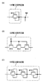
- the voltage holding circuit 120 includes a transistor M12 (see FIG. 1A).
- the first terminal (one of the source or the drain) of the transistor M12 is electrically connected to the voltage generation circuit 110, and the second terminal (the other of the source or the drain) of the transistor M12 is electrically connected to the node ND.
- the voltage holding circuit 120 has a function of turning on the transistor M12 and supplying the voltage VBG0 generated by the voltage generation circuit 110 to the node ND. Assuming that the threshold voltage of the transistor M12 is Vth1, when the transistor M12 is turned on, a voltage of VBG0 + Vth1 or more is preferably applied to the gate of the transistor M12. Further, the voltage holding circuit 120 has a function of holding the voltage of the node ND by turning off the transistor M12.
- the first gate and the second gate may be electrically connected to the second terminal by using a transistor having a first gate and a second gate in the transistor M12 (FIG. 4). (A)).
- the transistor M12 can function as a diode.
- Vg becomes 0 V when the first terminal is set to GND after a negative potential is supplied to the node ND. Therefore, it is preferable that Id (also referred to as “cutoff current”) when Vg is 0 V be small. By sufficiently reducing the cutoff current, the negative potential written to the node ND can be held for a long time.
- the channel length of the transistor M12 is preferably longer than the channel length of the transistor M11.
- the channel length of the transistor M12 is 1 ⁇ m or more, more preferably 3 ⁇ m or more, further preferably 5 ⁇ m or more, further preferably 10 ⁇ m or more.
- the transistor M12 can increase the breakdown voltage between the source and the drain. If the withstand voltage between the source and the drain of the transistor M12 is high, the connection between the voltage generation circuit 110 that generates a high voltage and the transistor M11 can be facilitated, which is preferable.
- an OS transistor or a transistor using a wide band gap semiconductor in a channel formation region is preferably used.
- a transistor using an OS transistor or a wide band gap semiconductor has a small cutoff current and a high withstand voltage between the source and the drain.
- a wide band gap semiconductor is a semiconductor having a band gap of 2.2 eV or more.
- silicon carbide, gallium nitride, diamond and the like can be mentioned.
- the transistor M12 is required to have a smaller cutoff current than the transistor M11.
- the transistor M11 is required to have a larger on current than the transistor M12.
- different transistors may be used to form the respective transistors.
- the transistor M12 preferably uses a semiconductor having a large band gap for the channel formation region, as compared to the transistor M11.
- a semiconductor with higher electron mobility is preferably used for the channel formation region than the transistor M12.
- the voltage holding circuit 120 may be configured by a plurality of transistors M12 connected in series (see FIGS. 4B and 4C).
- the temperature detection circuit 130 includes a temperature sensor 131 and an analog-digital conversion circuit (also referred to as “ADC”) 132 (see FIG. 5).
- ADC analog-digital conversion circuit
- the temperature sensor 131 has a function of sensing the temperature of the semiconductor device 100 and outputting an analog signal VA according to the temperature.
- a resistance temperature detector such as platinum, nickel, or copper, a thermistor, a thermocouple, an IC temperature sensor, or the like can be used.
- the analog-to-digital conversion circuit 132 has a function of converting the analog signal VA into an n-bit (n is an integer of 1 or more) digital signal VD.
- the digital signal VD is output from the temperature detection circuit 130 and supplied to the voltage control circuit 140.
- the temperature detection circuit 130 By converting the temperature information of the analog signal detected by the temperature detection circuit 130 into a digital signal and outputting the digital signal, it is possible to reduce the signal attenuation due to the wiring resistance and the parasitic capacitance and the influence of noise. Therefore, even when the temperature detection circuit 130 is provided at a position away from the voltage control circuit 140, temperature information can be accurately transmitted to the voltage control circuit 140.
- Voltage Control Circuit 140 As described with reference to FIG. 2A, as the temperature of the OS transistor is lower, Vth is shifted to the positive side, and the on-state current is decreased. As a result, the operating speed of the circuit is reduced. Also, as the temperature rises, Vth shifts to the negative side, and the cutoff current increases. This is a factor that narrows the operable temperature range for the circuit.
- the voltage control circuit 140 applies a correction voltage according to the operating temperature to the node ND to correct the voltage output from the output terminal VOUT of the semiconductor device 100, and a circuit electrically connected to the output terminal VOUT. Can extend the operable temperature range of
- the voltage control circuit 140 includes a logic circuit 145 and a voltage generation circuit 146 (see FIG. 1B).
- the logic circuit 145 has a function of supplying the digital signal (temperature information) supplied from the temperature detection circuit 130 to the voltage generation circuit 146.
- the serial signal supplied from the temperature detection circuit 130 is converted into a parallel signal and supplied to the voltage generation circuit 146.
- it has a function of converting an n-bit digital signal supplied from the temperature detection circuit 130 into an m-bit (m is an integer of 1 or more) digital signal and supplying the digital signal to the voltage generation circuit 146.
- the voltage generation circuit 146 has a function of converting the m-bit digital signal supplied from the logic circuit 145 into a voltage of 2 m steps and outputting it.
- FIG. 1B the case where m is 4 is illustrated.
- the voltage generation circuit 146 includes a buffer BF1, a buffer BF2, a buffer BF3, a buffer BF4, a capacitor C1, a capacitor C2, a capacitor C4, and a capacitor C8.
- the 4-bit digital signal output from the logic circuit 145 is supplied to the inputs of the buffers BF1 to BF4. Specifically, the first digit information of a 4-bit digital signal is input to buffer BF1, the second digit information is input to buffer BF2, the third digit information is input to buffer BF3, and the fourth digit Information is input to the buffer BF4.
- One electrode of the capacitive element C1 is electrically connected to the output of the buffer BF1, and the other electrode is electrically connected to the output terminal OUT.
- One electrode of the capacitive element C2 is electrically connected to the output of the buffer BF2, and the other electrode is electrically connected to the output terminal OUT.
- One electrode of the capacitive element C4 is electrically connected to the output of the buffer BF3, and the other electrode is electrically connected to the output terminal OUT.
- One electrode of the capacitive element C8 is electrically connected to the output of the buffer BF4, and the other electrode is electrically connected to the output terminal OUT.
- the voltage output from the output terminal OUT of the voltage control circuit 140 is called "voltage VBias".
- the output terminal OUT of the voltage control circuit 140 is electrically connected to the node ND of the semiconductor device 100.
- the voltage applied from the voltage control circuit 140 to the node ND is determined by the ratio of the combined capacitance of the capacitive element C1, the capacitive element C2, the capacitive element C4, and the capacitive element C8 to the parasitic capacitance generated at the node ND.
- the capacitance value of the capacitive element C1 is preferably sufficiently larger than the capacitance value of the parasitic capacitance. Specifically, the capacitance value of the capacitive element C1 is preferably 5 times or more, more preferably 10 times or more of the capacitance value of the parasitic capacitance.
- the capacitance values of the capacitive elements C1, C2, C4, and C8 may all be the same, but at least a part or all of them preferably have different capacitances.
- the capacitance value of the capacitance element C2 is twice as large as that of the capacitance element C1
- the capacitance value of the capacitance element C4 is four times as large as the capacitance value of the capacitance element C1
- the capacitance value of the capacitance element C8 is as capacitance.
- the capacitance value of the element C1 is eight times. By doing this, it is possible to supply 16-step voltages from the voltage control circuit 140 to the node ND.
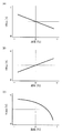
- FIGS. 6A to 6C show an example of the voltage change of the voltage VBias with respect to the temperature change.
- the horizontal axes of FIGS. 6A to 6C indicate the temperature on a linear scale.
- the vertical axes in FIGS. 6A to 6C indicate the voltage VBias on a linear scale.
- the magnitude of the voltage VBias preferably changes so as to decrease as the operating temperature of the transistor M11 increases (see FIG. 6A). Further, depending on the purpose and application, the operating temperature may be changed to be higher as the operating temperature is higher (see FIG. 6B). In addition, the magnitude of the voltage VBias may change non-linearly with temperature change (see FIG. 6C).
- the voltage change of the voltage VBias with respect to the temperature change can be set by the logic circuit 145.
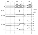
- FIG. 7 is a timing chart for explaining an operation example of the semiconductor device 100.
- the voltage VBias linearly changes in the range of 0 V to 7.5 V when the transistor M11 is an OS transistor and the operating temperature changes in the range of 100 ° C. to ⁇ 50 ° C. explain.
- the voltage VBG is ⁇ 3 V.
- a 4-bit digital signal VD is output from the temperature detection circuit 130.
- “0000” is output as the digital signal VD when the operating temperature is 100 ° C.
- “1111” is output when the operating temperature is ⁇ 50 ° C.
- the potential of the other electrode of the capacitive element C1 is increased by 0.5 V.
- the potential of the other electrode of the capacitive element C2 is increased by 1.0 V.
- the potential of the buffer BF3 connected to one electrode of the capacitive element C4 changes from the L potential to the H potential, the potential of the other electrode of the capacitive element C4 is increased by 2.0 V.
- the output of the buffer BF4 connected to one of the electrodes of the capacitive element C8 changes from the L potential to the H potential, the potential of the other electrode of the capacitive element C8 is increased by 4.0 V.
- Period T0 A period T0 is a reset period.
- the L potential (0 V) is output from each output of the buffers BF1 to BF4.
- the voltage VBG0 is set to -7 V to turn on the transistor M12. Therefore, the voltage VBG becomes -7V.
- the temperature detection circuit 130 may stop the output of the digital signal VD. Also, the operation of the temperature detection circuit 130 may be stopped.
- Period T1 In the period T1, the transistor M12 is turned off. The voltage of node ND is held at -7V. Therefore, the voltage VBG also remains at -7V.
- Period T2 the digital signal VD (temperature information) is supplied from the temperature detection circuit 130 to the voltage control circuit 140. For example, “1000” is supplied to the voltage control circuit 140 as a digital signal VD indicating 20 ° C.
- the logic circuit 145 inputs potentials corresponding to the digital signal VD to the buffers BF1 to BF4. Specifically, when the digital signal VD is "1000", the buffers BF1 to BF4 are controlled such that the outputs of the buffers BF1 to BF3 are at the L potential and the outputs of the buffer BF4 are at the H potential.
- the potential of the voltage control circuit 140 rises by 4V. Then, the voltage of the node ND changes from -7V to -3V, and the voltage VBG becomes -3V.
- Period T3 the digital signal VD (temperature information) is supplied from the temperature detection circuit 130 to the voltage control circuit 140. For example, “0101” is supplied to the voltage control circuit 140 as a digital signal VD indicating 50 ° C.
- the logic circuit 145 inputs a potential corresponding to the digital signal VD to the buffers BF1 to BF4.
- the digital signal VD is "0101”
- the output of the buffer BF1 is H potential
- the output of the buffer BF2 is L potential
- the output of the buffer BF3 is H potential
- the output of the buffer BF4 is L potential.
- the voltage VBG becomes -4.5V.
- Period T4 the digital signal VD (temperature information) is supplied from the temperature detection circuit 130 to the voltage control circuit 140.
- VD temperature information
- “1100” is supplied to the voltage control circuit 140 as a digital signal VD indicating ⁇ 20 ° C.
- the logic circuit 145 inputs potentials corresponding to the digital signal VD to the buffers BF1 to BF4.
- the digital signal VD is "1100”
- the output of the buffer BF1 is L potential
- the output of the buffer BF2 is L potential
- the output of the buffer BF3 is H potential
- the output of the buffer BF4 is H potential.
- the voltage VBG becomes -1.0V.
- the voltage VBG can be changed according to the temperature change.
- a voltage larger than necessary is applied to the second gate of the transistor M11. If a voltage larger than necessary is applied to the second gate of the transistor M11 for a long time, the electrical characteristics of the transistor M11 may be degraded, which may deteriorate the reliability.
- the voltage applied to the second gate of the transistor M11 can be changed in accordance with the temperature change. Therefore, the necessary minimum voltage can be applied to the second gate of the transistor M11. According to one embodiment of the present invention, the reliability of the semiconductor device including the transistor M11 can be improved.
- a reset period (period T0) may be provided for each fixed time to refresh the voltage of the node ND.
- This embodiment can be implemented in appropriate combination with the structures described in the other embodiments and the like.
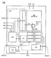
- FIG. 8 is a block diagram showing a configuration example of a storage device.
- the memory device 300 includes a peripheral circuit 311, a cell array 401, and the semiconductor device 100.
- the peripheral circuit 311 includes a row decoder 321, a word line driver circuit 322, a bit line driver circuit 330, an output circuit 340, and a control logic circuit 360.
- the word line driver circuit 322 has a function of supplying a potential to the wiring WL.
- the bit line driver circuit 330 includes a column decoder 331, a precharge circuit 332, an amplifier circuit 333, and a write circuit 334.
- the precharge circuit 332 has a function of precharging the wiring SL (not shown) and the like.
- the amplifier circuit 333 has a function of amplifying a data signal read from the wiring BIL or the wiring RBL. Note that the wiring WL, the wiring SL, the wiring BIL, and the wiring RBL are wirings connected to the memory cells 411 included in the cell array 401, and the details will be described later.
- the amplified data signal is output from the storage device 300 as a digital data signal RDATA through the output circuit 340.
- the storage device 300 is externally supplied with a low power supply voltage (VSS), a high power supply voltage (VDD) for the peripheral circuit 311, and a high power supply voltage (VIL) for the cell array 401 as power supply voltages.
- VSS low power supply voltage
- VDD high power supply voltage
- VIL high power supply voltage
- control signals CE, WE, RE
- an address signal ADDR a data signal WDATA
- CE, WE, RE control signals
- ADDR an address signal
- WDATA a data signal WDATA
- the control logic circuit 360 processes external input signals (CE, WE, RE) to generate control signals for the row decoder 321 and the column decoder 331.
- CE is a chip enable signal
- WE is a write enable signal
- RE is a read enable signal.
- the signal processed by the control logic circuit 360 is not limited to this, and another control signal may be input as necessary.
- An OS transistor can be applied to the transistors included in the cell array 401.
- an OS transistor can be applied to a transistor included in the peripheral circuit 311.
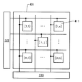
- FIG. 9 A configuration example of the cell array 401 is shown in FIG.
- the cell array 401 has m (n is an integer of 1 or more) in one column, n (n is an integer of 1 or more) in one row, and a total of m ⁇ n memory cells 411,
- the cells 411 are arranged in a matrix.
- the address of the memory cell 411 is also shown, and [1, 1], [m, 1], [i, j], [1, n], [m, n] (i is It is an integer of 1 or more and m or less, and j is a memory cell 411 located at an address of 1 or more and n or less.
- the number of wirings connecting the cell array 401 and the word line driver circuit 322 is determined by the configuration of the memory cells 411, the number of memory cells 411 included in one column, and the like. Further, the number of wirings connecting the cell array 401 and the bit line driver circuit 330 is determined by the configuration of the memory cells 411, the number of memory cells 411 included in one row, and the like.
- FIG. 10 shows a configuration example of the memory cells 411A to 411E applicable to the memory cell 411 described above.
- FIG. 10A shows a circuit configuration example of a DRAM type memory cell 411A.
- a DRAM using an OS transistor is called a DOSRAM (Dynamic Oxide Semiconductor Random Access Memory).
- the memory cell 411A includes a transistor M11 and a capacitive element CA.
- the first terminal of the transistor M11 is connected to the first terminal of the capacitive element CA, the second terminal of the transistor M11 is connected to the wiring BIL, the gate of the transistor M11 is connected to the wiring WL, and the back gate of the transistor M11 is Is connected to the wiring BGL.
- the second terminal of the capacitive element CA is connected to the wiring GNDL.
- the wiring GNDL is a wiring which provides a low level potential (sometimes referred to as a reference potential).
- the wiring BIL functions as a bit line, and the wiring WL functions as a word line.
- the wiring BGL functions as a wiring for applying a potential to the back gate of the transistor M11.
- the wiring BGL is electrically connected to the output terminal VOUT of the semiconductor device 100. By applying an arbitrary potential to the wiring BGL, the threshold voltage of the transistor M11 can be increased or decreased.
- Data writing and reading are performed by applying a high level potential to the wiring WL, turning on the transistor M11, and electrically connecting the wiring BIL to the first terminal of the capacitor CA.
- the memory cell included in the above-described storage device 300 is not limited to the memory cell 411A, and the circuit configuration can be changed.
- the transistor M11 is used for a memory cell, it is preferable to use an OS transistor as the transistor M11. Further, it is preferable to use an oxide semiconductor containing any one of indium, an element M (the element M is aluminum, gallium, yttrium, or tin), or zinc for the semiconductor layer of the OS transistor. In particular, an oxide semiconductor formed of indium, gallium, and zinc is preferably used.
- An OS transistor to which an oxide semiconductor containing indium, gallium, and zinc is applied has characteristics in which off current is extremely small.
- the leak current of the transistor M11 can be made extremely low. That is, since the written data can be held for a long time by the transistor M11, the frequency of refresh of the memory cell can be reduced. In addition, the refresh operation of the memory cell can be made unnecessary.
- the leakage current is extremely low, multilevel data or analog data can be held in the memory cell 411A, the memory cell 420, and the memory cell 430.
- a DOSRAM can be configured by applying an OS transistor as the transistor M11.
- FIG. 10B shows a circuit configuration example of a memory cell 411B of a gain cell type (also referred to as "2Tr1C type") having two transistors and one capacitance element.
- the memory cell 411B includes a transistor M11, a transistor M3, and a capacitive element CB.
- the first terminal of the transistor M11 is connected to the first terminal of the capacitive element CB, the second terminal of the transistor M11 is connected to the wiring WBL, the gate of the transistor M11 is connected to the wiring WL, and the back gate of the transistor M11 is Is connected to the wiring BGL.
- the second terminal of the capacitive element CB is connected to the wiring BL.
- the first terminal of the transistor M3 is connected to the wiring RBL, the second terminal of the transistor M3 is connected to the wiring SL, and the gate of the transistor M3 is connected to the first terminal of the capacitive element CB.
- the wiring WBL functions as a write bit line
- the wiring RBL functions as a read bit line
- the wiring WL functions as a word line.
- the wiring BL functions as a wiring for applying a predetermined potential to the second terminal of the capacitive element CB. At the time of data writing, it is preferable to apply a reference potential to the wiring BL during data retention.
- the wiring BGL functions as a wiring for applying a potential to the back gate of the transistor M11.
- the wiring BGL is electrically connected to the output terminal VOUT of the semiconductor device 100. By applying an arbitrary potential to the wiring BGL, the threshold voltage of the transistor M11 can be increased or decreased.
- Data writing is performed by applying a high level potential to the wiring WL, turning on the transistor M11, and electrically connecting the wiring WBL to the first terminal of the capacitor CB. Specifically, when the transistor M11 is in a conductive state, a potential corresponding to data to be recorded is applied to the wiring WBL, and the potential is written to the first terminal of the capacitor CB and the gate of the transistor M3. After that, a low level potential is applied to the wiring WL and the transistor M11 is turned off, whereby the potential of the first terminal of the capacitor CB and the potential of the gate of the transistor M3 are held.
- Data is read out by applying a predetermined potential to the wirings BL and SL. Since the current flowing between the source and drain of the transistor M3 and the potential of the first terminal of the transistor M3 are determined by the potential of the gate of the transistor M3 and the potential of the second terminal of the transistor M3, they are connected to the first terminal of the transistor M3
- the potential held at the first terminal of the capacitive element CB (or the gate of the transistor M3) can be read. That is, the information written in the memory cell can be read from the potential held at the first terminal of the capacitor element CB (or the gate of the transistor M3).
- the presence or absence of information written in this memory cell can be known.
- the memory cell included in the above-described storage device 300 is not limited to the memory cell 411B, and the circuit configuration can be changed as appropriate.
- the wiring WBL and the wiring RBL may be combined into one wiring BIL.
- An example of circuit configuration of the memory cell is shown in FIG.
- the memory cell 411C has a configuration in which the second terminal of the transistor M11 and the first terminal of the transistor M3 are connected to the wiring BIL, with the wiring WBL and the wiring RBL of the memory cell 411B as one wiring BIL. . That is, the memory cell 411C is configured to operate as the write bit line and the read bit line as one wire BIL.
- an OS transistor is preferably used as the transistor M11 also in the memory cell 411B.
- a memory device using a 2Tr1C type memory cell such as the memory cell 411B and the memory cell 411C by using an OS transistor for the transistor M11 is referred to as a non-volatile oxide semiconductor random access memory (NOSRAM).
- NOSRAM non-volatile oxide semiconductor random access memory
- silicon is preferably included in the channel formation region of the transistor M3.
- the silicon can be amorphous silicon, polycrystalline silicon, low temperature poly-silicon (LTPS) (hereinafter referred to as Si transistor). Since the Si transistor may have a field effect mobility higher than that of the OS transistor, it is preferable to apply the Si transistor as the read transistor.
- LTPS low temperature poly-silicon
- the memory cell can be configured as a unipolar circuit.
- FIG. 10D shows a circuit configuration example of a memory cell 411D of a gain cell type (also referred to as “3Tr1C type”) of three transistors and one capacitance element.
- the memory cell 411D includes a transistor M11, a transistor M5, a transistor M6, and a capacitive element CC.
- the first terminal of the transistor M11 is connected to the first terminal of the capacitive element CC
- the second terminal of the transistor M11 is connected to the wiring BIL
- the gate of the transistor M11 is connected to the wiring WL
- the back gate of the transistor M11 is Are electrically connected to the wiring BGL.
- the second terminal of the capacitive element CC is electrically connected to the first terminal of the transistor M5 and the wiring GNDL.
- the second terminal of the transistor M5 is connected to the first terminal of the transistor M6, and the gate of the transistor M5 is connected to the first terminal of the capacitive element CC.
- the second terminal of the transistor M6 is connected to the wiring BIL, and the gate of the transistor M6 is connected to the wiring RL.
- the wiring BIL functions as a bit line
- the wiring WL functions as a write word line
- the wiring RL functions as a read word line.
- the wiring BGL functions as a wiring for applying a potential to the back gate of the transistor M11.
- the wiring BGL is electrically connected to the output terminal VOUT of the semiconductor device 100. By applying an arbitrary potential to the wiring BGL, the threshold voltage of the transistor M11 can be increased or decreased.
- Data writing is performed by applying a high level potential to the wiring WL, turning on the transistor M11, and connecting the wiring BIL to the first terminal of the capacitor CC. Specifically, when the transistor M11 is in a conductive state, a potential corresponding to the information to be recorded is applied to the wiring BIL, and the potential is written to the first terminal of the capacitive element CC and the gate of the transistor M5. After that, a low level potential is applied to the wiring WL and the transistor M11 is turned off, whereby the potential of the first terminal of the capacitor CC and the potential of the gate of the transistor M5 are held.
- Data is read out by precharging the wiring BIL with a predetermined potential, then electrically floating the wiring BIL and applying a high level potential to the wiring RL. Since the wiring RL has a high level potential, the transistor M6 is turned on, and the wiring BIL and the second terminal of the transistor M5 are electrically connected. At this time, the potential of the wiring BIL is applied to the second terminal of the transistor M5, but the transistor is selected according to the potential held by the first terminal of the capacitive element CC (or the gate of the transistor M5). The potential of the second terminal of M5 and the potential of the wiring BIL change.
- the potential held in the first terminal of the capacitive element CC (or the gate of the transistor M5) can be read out. That is, the information written in the memory cell can be read from the potential held at the first terminal of the capacitive element CC (or the gate of the transistor M5). Alternatively, the presence or absence of information written in this memory cell can be known.
- the configuration of the circuit can be changed as appropriate.
- the 3Tr1C type memory cell 411D to which the OS transistor is applied as the transistor M11 is an aspect of the NOSRAM described above.
- silicon is preferably included in the channel formation regions of the transistors M5 and M6 described in this embodiment.
- the silicon can be amorphous silicon, polycrystalline silicon, low temperature polysilicon. Since the Si transistor may have a field effect mobility higher than that of the OS transistor, it is preferable to apply the Si transistor as the read transistor.
- the memory cell can be configured as a unipolar circuit.
- FIG. 10E shows an example of a circuit configuration of a memory cell 411E of static random access memory (SRAM) type using an OS transistor.
- SRAM static random access memory
- an SRAM using an OS transistor is called oxSRAM.
- a memory cell 411E illustrated in FIG. 10E is a SRAM memory cell that can be backed up.
- the memory cell 411E includes transistors M7 to M10, transistors MS1 to MS4, a capacitive element CD1, and a capacitive element CD2.
- the transistor M7 and the transistor M8 correspond to the transistor M11.
- the transistors M7 to M10 are transistors each having a back gate.
- the transistor MS1 and the transistor MS2 are p-channel transistors, and the transistor MS3 and the transistor MS4 are n-channel transistors.
- the first terminal of the transistor M7 is connected to the wiring BIL, and the second terminal of the transistor M7 is the first terminal of the transistor MS1, the first terminal of the transistor MS3, the gate of the transistor MS2, and the gate of the transistor MS4. And the first terminal of the transistor M10.
- the gate of the transistor M7 is connected to the wiring WL, and the back gate of the transistor M7 is connected to the wiring BGL1.
- the first terminal of the transistor M8 is connected to the wiring BILB, and the second terminal of the transistor M8 is the first terminal of the transistor MS2, the first terminal of the transistor MS4, the gate of the transistor MS1, and the gate of the transistor MS3. And the first terminal of the transistor M9.
- the gate of the transistor M8 is connected to the wiring WL, and the back gate of the transistor M8 is connected to the wiring BGL2.
- the second terminal of the transistor MS1 is electrically connected to the wiring VDL.
- the second terminal of the transistor MS2 is electrically connected to the wiring VDL.
- the second terminal of the transistor MS3 is electrically connected to the wiring GNDL.
- the second terminal of the transistor MS4 is connected to the wiring GNDL.
- the second terminal of the transistor M9 is connected to the first terminal of the capacitive element CD1, the gate of the transistor M9 is connected to the wiring BRL, and the back gate of the transistor M9 is connected to the wiring BGL3.
- the second terminal of the transistor M10 is connected to the first terminal of the capacitive element CD2, the gate of the transistor M10 is connected to the wiring BRL, and the back gate of the transistor M10 is connected to the wiring BGL4.
- the second terminal of the capacitive element CD1 is connected to the wiring GNDL, and the second terminal of the capacitive element CD2 is connected to the wiring GNDL.
- the wiring BIL and the wiring BILB function as bit lines
- the wiring WL functions as a word line
- the wiring BRL is a wiring that controls the on / off states of the transistor M9 and the transistor M10.
- the wirings BGL1 to BGL4 function as wirings for applying a potential to back gates of the transistors M7 to M10, respectively.
- the wirings BGL1 to BGL4 are electrically connected to the output terminal VOUT of the semiconductor device 100.
- a plurality of semiconductor devices 100 may be provided in the memory device 300, and the wirings BGL1 to BGL4 may be electrically connected to different semiconductor devices 100.
- the threshold voltage of each of the transistors M7 to M10 can be increased or decreased.
- the wiring VDL is a wiring giving a high level potential
- the wiring GNDL is a wiring giving a low level potential.
- Data writing is performed by applying a high level potential to the wiring WL and applying a high level potential to the wiring BRL. Specifically, when the transistor M10 is in a conductive state, a potential corresponding to the information to be recorded is applied to the wiring BIL, and the potential is written to the second terminal side of the transistor M10.
- the memory cell 411E forms an inverter loop by the transistors MS1 and MS2, the inverted signal of the data signal corresponding to the potential is input to the second terminal side of the transistor M8. Since the transistor M8 is in a conductive state, a potential applied to the wiring BIL, that is, an inverted signal of a signal input to the wiring BIL is output to the wiring BILB. Further, since the transistor M9 and the transistor M10 are in a conductive state, the potential of the second terminal of the transistor M7 and the potential of the second terminal of the transistor M8 are the first terminal of the capacitive element CD2 and the first terminal of the capacitive element CD1, respectively. It is held by 1 terminal.
- a low level potential is applied to the wiring WL, a low level potential is applied to the wiring BRL, and the transistors M7 to M10 are turned off, whereby the potential of the first terminal of the capacitive element CD1 and the capacitive element Hold the potential of the first terminal of the CD2.
- OS transistors are preferably used as the transistors M7 to M10.
- OS transistors are preferably used as the transistors M7 to M10.
- data written to the memory cell 411E can be held for a long time, so that the frequency of refresh of the memory cell 411E can be reduced.
- the refresh operation of the memory cell 411E can be eliminated.
- the leakage current is very low, multilevel data or analog data can be held in the memory cell 411E.
- silicon is preferably included in channel formation regions of the transistors MS1 to MS4.
- the silicon can be amorphous silicon, polycrystalline silicon, low temperature polysilicon.
- the field effect mobility of the Si transistor may be higher than that of the OS transistor. Therefore, it is preferable to apply the Si transistor as a transistor included in the inverter.
- One semiconductor device 100 may be electrically connected to all the memory cells.
- a plurality of semiconductor devices 100 may be provided in the memory device 300, and a plurality of memory cells may be electrically connected to one semiconductor device 100 for each column or for each column.
- a plurality of memory cells may be electrically connected to one semiconductor device 100 for each row or for each plurality of rows.
- the plurality of memory cells included in the cell array may be divided into a plurality of blocks, and one semiconductor device 100 may be provided for each block or for each plurality of blocks.
- the memory cell described in this embodiment can be used as a memory element such as a register and a cache included in a CPU, a GPU, or the like.
- This embodiment can be implemented in appropriate combination with the structures described in the other embodiments and the like.
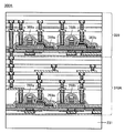
- FIG. 11 shows a cross section of part of the storage device 300.
- a memory device 300 illustrated in FIG. 11 has a layer 310 and a layer 320 stacked over a substrate 231.
- FIG. 11 shows the case where a single crystal semiconductor substrate (for example, a single crystal silicon substrate) is used as the substrate 231.
- the layer 310 includes, over a substrate 231, a transistor 233a, a transistor 233b, and a transistor 233c.
- FIG. 11 illustrates a cross section in the channel length direction of the transistor 233a, the transistor 233b, and the transistor 233c.
- Channels of the transistors 233 a, 233 b, and 233 c are formed in part of the substrate 231.
- a single crystal semiconductor substrate is preferably used as the substrate 231.
- the transistor 233 a, the transistor 233 b, and the transistor 233 c are electrically isolated by the element isolation layer 232.
- a LOCOS (Local Oxidation of Silicon) method, an STI (Shallow Trench Isolation) method, or the like can be used.
- the insulating layer 234 is provided over the substrate 231, the insulating layer 235 and the insulating layer 237 are provided over the transistor 233a, the transistor 233b, and the transistor 233c, and the electrode 238 is embedded in the insulating layer 237.
- the electrode 238 is electrically connected to one of the source and the drain of the transistor 233 a through the contact plug 236.
- the insulating layer 239, the insulating layer 240, and the insulating layer 241 are provided over the electrode 238 and the insulating layer 237, and the electrode 242 is embedded in the insulating layer 239, the insulating layer 240, and the insulating layer 241. .
- the electrode 242 is electrically connected to the electrode 238.
- the insulating layer 243 and the insulating layer 244 are provided over the electrode 242 and the insulating layer 241, and the electrode 245 is embedded in the insulating layer 243 and the insulating layer 244.
- the electrode 245 is electrically connected to the electrode 242.
- the insulating layer 246 and the insulating layer 247 are provided over the electrode 245 and the insulating layer 244, and the electrode 249 is embedded in the insulating layer 246 and the insulating layer 247.
- the electrode 249 is electrically connected to the electrode 245.
- the insulating layer 248 and the insulating layer 250 are provided over the electrode 249 and the insulating layer 247, and the electrode 251 is embedded in the insulating layer 248 and the insulating layer 250.
- the electrode 251 is electrically connected to the electrode 249.
- Layer 320 is provided on layer 310.
- the layer 320 includes a transistor 368a, a transistor 368b, a capacitor 369a, and a capacitor 369b.
- FIG. 11 illustrates a cross section in the channel length direction of the transistor 368a and the transistor 368b. Note that the transistor 368a and the transistor 368b are transistors having a back gate.
- the transistor 368a and the transistor 368b correspond to the transistor M11 described in the above embodiment.
- an oxide semiconductor which is a kind of metal oxide is preferably used for the semiconductor layers of the transistors 368a and 368b. That is, it is preferable to use an OS transistor for the transistor 368a and the transistor 368b.
- the transistor 368 a and the transistor 368 b are provided over the insulating layer 361 and the insulating layer 362.
- an insulating layer 363 and an insulating layer 364 are provided over the insulating layer 362.
- the back gates of the transistor 368 a and the transistor 368 b are embedded in the insulating layer 363 and the insulating layer 364.
- An insulating layer 365 and an insulating layer 366 are provided over the insulating layer 364.
- the electrode 367 is embedded in the insulating layer 361 to the insulating layer 366. The electrode 367 is electrically connected to the electrode 251.
- the insulating layer 371, the insulating layer 372, and the insulating layer 373 are formed over the transistor 368a, the transistor 368b, the capacitor 369a, and the capacitor 369b, and the electrode 375 is formed over the insulating layer 373.
- the electrode 375 is electrically connected to the electrode 367 through the contact plug 374.
- an insulating layer 376, an insulating layer 377, an insulating layer 378, and an insulating layer 379 are provided over the electrode 375.
- the electrode 380 is embedded in the insulating layer 376 to the insulating layer 379. The electrode 380 is electrically connected to the electrode 375.
- an insulating layer 381 and an insulating layer 382 are provided over the electrode 380 and the insulating layer 379.
- FIG. 12 shows a cross section of part of the storage device 300A.
- the storage device 300A is a modification of the storage device 300.
- the storage device 300A has a layer 310A and a layer 320.
- an insulating substrate for example, a glass substrate
- the layer 310A includes a transistor 268a, a transistor 268b, and a capacitor 269a.
- a thin film transistor eg, an OS transistor
- the layer 310A can be a single-polar integrated circuit.
- the storage device 300A can be a unipolar storage device.
- the material used as the substrate there is no particular limitation on the material used as the substrate, but at least a heat resistance that can withstand the later heat treatment is required.
- a single crystal semiconductor substrate made of silicon, silicon carbide or the like, a polycrystalline semiconductor substrate, a compound semiconductor substrate made of silicon germanium or the like can be used as a substrate.
- an SOI substrate, or a semiconductor substrate on which semiconductor elements such as a strain transistor or a FIN transistor are provided can be used.
- gallium arsenide, aluminum gallium arsenide, indium gallium arsenide, gallium nitride, indium phosphide, silicon germanium, or the like applicable to a high electron mobility transistor (HEMT) may be used. That is, the substrate is not limited to a simple support substrate, and may be a substrate on which devices such as other transistors are formed.
- a glass substrate such as barium borosilicate glass or aluminoborosilicate glass, a ceramic substrate, a quartz substrate, a sapphire substrate, or the like can be used.
- a flexible substrate flexible substrate
- a transistor, a capacitor, or the like may be manufactured directly on the flexible substrate, or a transistor, a capacitor, or the like may be manufactured on another manufacturing substrate, and then the flexible substrate is manufactured. It may be exfoliated or displaced. Note that in order to peel and transfer the manufacturing substrate to the flexible substrate, a peeling layer may be provided between the manufacturing substrate and the transistor, the capacitor, or the like.
- the flexible substrate for example, metal, alloy, resin or glass, or fibers thereof can be used.
- a flexible substrate used for the substrate for example, a material having a linear expansion coefficient of 1 ⁇ 10 ⁇ 3 / K or less, 5 ⁇ 10 ⁇ 5 / K or less, or 1 ⁇ 10 ⁇ 5 / K or less may be used.
- the resin include polyester, polyolefin, polyamide (such as nylon and aramid), polyimide, polycarbonate, and acrylic.
- aramid is suitable as a flexible substrate because of its low coefficient of linear expansion.
- the insulating layer is aluminum nitride, aluminum oxide, aluminum nitride oxide, aluminum oxynitride, magnesium oxide, silicon oxide, silicon oxide, silicon nitride oxide, silicon oxynitride, silicon oxynitride, gallium oxide, germanium oxide, yttrium oxide, zirconium oxide, lanthanum oxide,
- a material selected from neodymium oxide, hafnium oxide, tantalum oxide, aluminum silicate and the like is used in a single layer or laminated form.
- a material obtained by mixing a plurality of materials among an oxide material, a nitride material, an oxynitride material, and a nitride oxide material may be used.
- the nitrided oxide refers to a compound having a higher content of nitrogen than oxygen.
- oxynitride refers to a compound having a higher content of oxygen than nitrogen.
- the content of each element can be measured, for example, using Rutherford Backscattering Spectroscopy (RBS) or the like.
- the hydrogen concentration in the insulating layer is 2 ⁇ 10 20 atoms / cm 3 or less, preferably 5 ⁇ 10 19 atoms / cm 3 or less, in secondary ion mass spectrometry (SIMS). More preferably, it is 1 ⁇ 10 19 atoms / cm 3 or less, more preferably 5 ⁇ 10 18 atoms / cm 3 or less. In particular, it is preferable to reduce the hydrogen concentration in the insulating layer in contact with the semiconductor layer.
- the nitrogen concentration in the insulating layer is 5 ⁇ 10 19 atoms / cm 3 or less, preferably 5 ⁇ 10 18 atoms / cm 3 or less, more preferably 1 ⁇ 10 18 atoms / cm 3 or less in SIMS. More preferably, it is 5 ⁇ 10 17 atoms / cm 3 or less.
- the insulating layer in contact with the semiconductor layer preferably has few defects, and typically, it is preferable that a signal observed by electron spin resonance (ESR) be small.
- the above-mentioned signal includes the E ′ center observed at a g value of 2.001.
- the E 'center is due to dangling bonds of silicon.
- the spin density derived from the E ′ center is 3 ⁇ 10 17 spins / cm 3 or less, preferably 5 ⁇ 10 16 spins / cm 3 or less
- a silicon oxide layer or a silicon oxynitride layer may be used.
- signals derived from nitrogen dioxide (NO 2 ) may be observed.
- the signal is divided into three signals by N nuclear spins, and each g value is 2.037 or more and 2.039 or less (referred to as a first signal), and the g value is 2.001 or more and 2.03.
- the following referred to as a second signal
- g values of 1.964 or more and 1.966 or less are observed.
- an insulating layer in which a spin density of a signal derived from nitrogen dioxide (NO 2 ) is 1 ⁇ 10 17 spins / cm 3 or more and 1 ⁇ 10 18 spins / cm 3 or less.
- NO 2 nitrogen dioxide
- nitrogen oxides (NO x ) containing nitrogen dioxide (NO 2 ) form energy levels in the insulating layer.
- the level is located in the energy gap of the oxide semiconductor layer. Therefore, when nitrogen oxide (NO x ) diffuses to the interface between the insulating layer and the oxide semiconductor layer, the level may trap electrons on the insulating layer side. As a result, trapped electrons remain in the vicinity of the interface between the insulating layer and the oxide semiconductor layer, which shifts the threshold voltage of the transistor in the positive direction. Therefore, when a film with a low content of nitrogen oxide is used as the insulating layer, the shift in threshold voltage of the transistor can be reduced.
- a silicon oxynitride layer can be used as the insulating layer in which the amount of released nitrogen oxide (NO x ) is small.
- the silicon oxynitride layer is a film in which the amount of released ammonia is larger than the amount of released nitrogen oxide (NO x ) in thermal desorption spectroscopy (TDS), and typically, ammonia is used.
- the released amount is 1 ⁇ 10 18 molecules / cm 3 or more and 5 ⁇ 10 19 molecules / cm 3 or less. Note that the above release amount of ammonia is the total amount of the heat treatment temperature in TDS in the range of 50 ° C. to 650 ° C., or 50 ° C. to 550 ° C.
- nitrogen oxides (NO x ) react with ammonia and oxygen in heat treatment, nitrogen oxides (NO x ) are reduced by using an insulating layer with a large amount of released ammonia.
- At least one of the insulating layers in contact with the oxide semiconductor layer is preferably formed using an insulating layer from which oxygen is released by heating.
- an insulating layer from which oxygen is released by heating is 1.0. It is preferable to use an insulating layer which is 10 18 atoms / cm 3 or more, 1.0 10 19 atoms / cm 3 or more, or 1.0 10 20 atoms / cm 3 or more.
- oxygen released by heating is also referred to as “excess oxygen”.
- the insulating layer containing excess oxygen can be formed by performing treatment for adding oxygen to the insulating layer.
- the process of adding oxygen can be performed by heat treatment in an oxidizing atmosphere, plasma treatment, or the like.
- oxygen may be added using an ion implantation method, an ion doping method, a plasma immersion ion implantation method, or the like.
- the gas used for the process of adding oxygen include gases containing oxygen, such as oxygen gas such as 16 O 2 or 18 O 2 , nitrous oxide gas, or ozone gas.
- the process of adding oxygen is also referred to as "oxygen doping process". Oxygen doping may be performed by heating the substrate.
- a heat-resistant organic material such as polyimide, an acrylic resin, a benzocyclobutene resin, a polyamide, or an epoxy resin can be used.
- organic materials low dielectric constant materials (low-k materials), siloxane resins, PSG (phosphorus glass), BPSG (phosphorus boron glass), and the like can be used.
- the insulating layer may be formed by stacking a plurality of insulating layers formed of any of these materials.
- a siloxane-based resin corresponds to a resin including a Si-O-Si bond formed using a siloxane-based material as a starting material.
- the siloxane-based resin may use an organic group (for example, an alkyl group or an aryl group) or a fluoro group as a substituent.
- the organic group may have a fluoro group.
- the method of forming the insulating layer is not particularly limited. Note that depending on the material used for the insulating layer, a firing step may be required. In this case, by combining the baking step of the insulating layer and another heat treatment step, a transistor can be efficiently manufactured.
- Conductive materials for forming the electrode include aluminum, chromium, copper, silver, gold, platinum, tantalum, nickel, titanium, molybdenum, tungsten, hafnium, vanadium, niobium, manganese, magnesium, zirconium, beryllium, indium and the like
- a material containing one or more metal elements selected from the above can be used.
- a semiconductor with high electrical conductivity typically a polycrystalline silicon containing an impurity element such as phosphorus, or a silicide such as nickel silicide may be used.
- a conductive material containing the above metal element and oxygen may be used.
- a conductive material containing the above metal element and nitrogen may be used.
- a conductive material containing nitrogen such as titanium nitride or tantalum nitride may be used.
- indium tin oxide (ITO) indium oxide containing tungsten oxide, indium zinc oxide containing tungsten oxide, indium oxide containing titanium oxide, indium tin oxide containing titanium oxide, indium zinc An oxide, indium gallium zinc oxide, or indium tin oxide doped with silicon may be used.
- indium gallium zinc oxide containing nitrogen may be used.
- a plurality of conductive layers formed of the above materials may be stacked.
- a stacked structure in which a material containing a metal element described above and a conductive material containing oxygen are combined may be used.
- a stacked structure in which the material containing the metal element described above and the conductive material containing nitrogen are combined may be used.
- a stacked structure in which the above-described material containing a metal element, the conductive material containing oxygen, and the conductive material containing nitrogen are combined may be used.
- a stacked structure in which a conductive material containing nitrogen and a conductive material containing oxygen are combined may be used.
- the conductive material containing oxygen is used as a semiconductor It is good to provide on the layer side. By providing the conductive material containing oxygen on the semiconductor layer side, oxygen released from the conductive material can be easily supplied to the semiconductor layer.
- a conductive material having high embedding property such as tungsten or polysilicon may be used.
- a conductive material having high embeddability and a barrier layer (diffusion prevention layer) such as a titanium layer, a titanium nitride layer, or a tantalum nitride layer may be used in combination.
- an electrode may be called a "contact plug.”
- a conductive material which hardly transmits impurities to an electrode in contact with the gate insulating layer is preferably used.
- An example of the conductive material which is hard to transmit impurities is tantalum nitride.
- the reliability of the transistor can be further enhanced. That is, the reliability of the storage device can be further enhanced.
- semiconductor layer a single crystal semiconductor, a polycrystalline semiconductor, a microcrystalline semiconductor, an amorphous semiconductor, or the like can be used alone or in combination.
- a semiconductor material silicon, germanium, or the like can be used, for example.
- a compound semiconductor such as silicon germanium, silicon carbide, gallium arsenide, an oxide semiconductor, or a nitride semiconductor, an organic semiconductor, or the like can be used.
- a low molecular weight organic material having an aromatic ring, a ⁇ electron conjugated conductive polymer, or the like can be used.
- a low molecular weight organic material having an aromatic ring, a ⁇ electron conjugated conductive polymer, or the like can be used.
- rubrene, tetracene, pentacene, perylene diimide, tetracyanoquinodimethane, polythiophene, polyacetylene, polyparaphenylene vinylene and the like can be used.
- semiconductor layers may be stacked. In the case of stacking semiconductor layers, semiconductors having different crystal states may be used, or semiconductor materials different from each other may be used.
- the band gap of an oxide semiconductor which is a kind of metal oxide is 2 eV or more
- the off current per ⁇ m of the channel width is less than 1 ⁇ 10 ⁇ 20 A, 1 ⁇ 10 ⁇ 22 A It may be less than 1 or less than 1 ⁇ 10 -24 A. That is, the on / off ratio can be 20 digits or more.
- a transistor in which an oxide semiconductor is used for a semiconductor layer has high withstand voltage between the source and the drain.
- a transistor with high reliability can be provided.
- a transistor with a large output voltage and high withstand voltage can be provided.
- a storage device with high reliability can be provided.
- a memory device with a large output voltage and high withstand voltage can be provided.
- a transistor in which silicon having crystallinity is used for a semiconductor layer in which a channel is formed is also referred to as a “crystalline Si transistor”.
- Crystalline Si transistors are easier to obtain relatively higher mobility than OS transistors.
- OS transistors it is difficult to realize extremely low off current like OS transistors. Therefore, it is important to properly use the semiconductor material used for the semiconductor layer in accordance with the purpose and application.
- an OS transistor and a crystalline Si transistor may be used in combination depending on the purpose and application.
- the oxide semiconductor layer is preferably formed by a sputtering method.
- the oxide semiconductor layer is preferably formed by a sputtering method because the density of the oxide semiconductor layer can be increased.
- a rare gas typically, argon
- oxygen or a mixed gas of a rare gas and oxygen may be used as a sputtering gas.
- high purification of the sputtering gas is also required.
- an oxygen gas or a rare gas which is used as a sputtering gas is a gas which is highly purified to a dew point of ⁇ 60 ° C. or less, preferably ⁇ 100 ° C. or less.
- the oxide semiconductor layer is formed by a sputtering method
- Metal oxide An oxide semiconductor which is a kind of metal oxide preferably contains at least indium or zinc. In particular, it is preferable to contain indium and zinc. In addition to them, aluminum, gallium, yttrium or tin is preferably contained. In addition, one or more selected from boron, silicon, titanium, iron, nickel, germanium, zirconium, molybdenum, lanthanum, cerium, neodymium, hafnium, tantalum, tungsten, or magnesium may be included.
- the oxide semiconductor contains indium, an element M, and zinc.
- the element M is aluminum, gallium, yttrium, tin or the like.
- Other elements applicable to the element M include boron, silicon, titanium, iron, nickel, germanium, zirconium, molybdenum, lanthanum, cerium, neodymium, hafnium, tantalum, tungsten, magnesium and the like.
- the element M a plurality of the aforementioned elements may be combined in some cases.
- metal oxides having nitrogen may also be collectively referred to as metal oxides.
- a metal oxide having nitrogen may be referred to as metal oxynitride.
- CAC Cloud-Aligned Composite
- CAAC c-axis aligned crystal
- CAC Cloud-Aligned Composite
- the CAC-OS or CAC-metal oxide has a conductive function in part of the material and an insulating function in part of the material, and functions as a semiconductor throughout the material.
- the conductive function is a function of allowing electrons (or holes) to be carriers
- the insulating function is a carrier. It is a function that does not flow electrons.
- a function of switching can be imparted to the CAC-OS or the CAC-metal oxide by causing the conductive function and the insulating function to be complementary to each other.
- CAC-OS or CAC-metal oxide has a conductive region and an insulating region.
- the conductive region has the above-mentioned conductive function
- the insulating region has the above-mentioned insulating function.
- the conductive region and the insulating region may be separated at the nanoparticle level.
- the conductive region and the insulating region may be unevenly distributed in the material.
- the conductive region may be observed as connected in a cloud shape with a blurred periphery.
- the conductive region and the insulating region are each dispersed in the material with a size of 0.5 nm or more and 10 nm or less, preferably 0.5 nm or more and 3 nm or less There is.
- CAC-OS or CAC-metal oxide is composed of components having different band gaps.
- CAC-OS or CAC-metal oxide is composed of a component having a wide gap resulting from the insulating region and a component having a narrow gap resulting from the conductive region.
- carriers flow mainly in the component having the narrow gap.
- the component having the narrow gap acts complementarily to the component having the wide gap, and the carrier also flows to the component having the wide gap in conjunction with the component having the narrow gap. Therefore, when the above-described CAC-OS or CAC-metal oxide is used for a channel formation region of a transistor, high current driving force, that is, high on current, and high field effect mobility can be obtained in the on state of the transistor.
- CAC-OS or CAC-metal oxide can also be called a matrix composite (matrix composite) or a metal matrix composite (metal matrix composite).
- An oxide semiconductor which is a kind of metal oxide can be divided into a single crystal oxide semiconductor and other non-single crystal oxide semiconductors.
- the non-single crystal oxide semiconductor for example, c-axis aligned crystalline oxide semiconductor (CAAC-OS), polycrystalline oxide semiconductor, nanocrystalline oxide semiconductor (nc-OS), pseudo amorphous oxide semiconductor (a-like) OS: amorphous-like oxide semiconductor) and amorphous oxide semiconductor.
- the CAAC-OS has c-axis orientation, and a plurality of nanocrystals are connected in the a-b plane direction to form a strained crystal structure.
- distortion refers to a portion where the orientation of the lattice arrangement changes between the region in which the lattice arrangement is aligned and the region in which another lattice arrangement is aligned in the region where the plurality of nanocrystals are connected.
- the nanocrystals are based on hexagons, but may not be regular hexagons and may be non-hexagonal. Moreover, distortion may have a lattice arrangement such as pentagon and heptagon. Note that in the CAAC-OS, it is difficult to confirm clear crystal grain boundaries (also referred to as grain boundaries) even in the vicinity of strain. That is, it is understood that the formation of crystal grain boundaries is suppressed by the distortion of the lattice arrangement. This is because the CAAC-OS can tolerate distortion due to the fact that the arrangement of oxygen atoms is not dense in the a-b plane direction, or that the bonding distance between atoms is changed due to metal element substitution. It is for.
- a CAAC-OS is a layered crystal in which a layer containing indium and oxygen (hereinafter referred to as In layer) and a layer containing element M, zinc and oxygen (hereinafter referred to as (M, Zn) layer) are stacked. It tends to have a structure (also referred to as a layered structure).
- In layer a layer containing indium and oxygen
- M, Zn zinc and oxygen
- indium and the element M can be substituted with each other, and when the element M in the (M, Zn) layer is substituted with indium, it can also be expressed as an (In, M, Zn) layer.
- indium in the In layer is substituted with the element M, it can also be represented as an (In, M) layer.
- CAAC-OS is a highly crystalline metal oxide. On the other hand, it is difficult to confirm clear crystal grain boundaries in CAAC-OS, so it can be said that the decrease in electron mobility due to crystal grain boundaries does not easily occur. In addition, since the crystallinity of the metal oxide may be lowered due to the mixing of impurities, generation of defects, or the like, CAAC-OS can also be said to be a metal oxide with few impurities or defects (such as oxygen vacancies). Therefore, the metal oxide having a CAAC-OS has stable physical properties. Therefore, a metal oxide having a CAAC-OS is resistant to heat and has high reliability.
- the nc-OS has periodicity in atomic arrangement in a minute region (eg, a region of 1 nm to 10 nm, particularly a region of 1 nm to 3 nm).
- nc-OS has no regularity in crystal orientation among different nanocrystals. Therefore, no orientation can be seen in the entire film. Therefore, the nc-OS may not be distinguished from the a-like OS or the amorphous oxide semiconductor depending on the analysis method.
- the a-like OS is a metal oxide having a structure between nc-OS and an amorphous oxide semiconductor.
- the a-like OS has a wrinkle or low density region. That is, a-like OS has lower crystallinity than nc-OS and CAAC-OS.
- Oxide semiconductors have various structures, and each has different characteristics.
- the oxide semiconductor may have two or more of an amorphous oxide semiconductor, a polycrystalline oxide semiconductor, an a-like OS, an nc-OS, and a CAAC-OS.
- a metal oxide with low carrier density is preferably used for the transistor.
- the impurity concentration in the metal oxide film may be lowered to lower the density of defect states.
- a low impurity concentration and a low density of defect levels are referred to as high purity intrinsic or substantially high purity intrinsic.
- the metal oxide has a carrier density of less than 8 ⁇ 10 11 / cm 3 , preferably less than 1 ⁇ 10 11 / cm 3 , more preferably less than 1 ⁇ 10 10 / cm 3 , and 1 ⁇ 10 ⁇ 9 / cm 3. It should be cm 3 or more.
- the trap state density may also be low.
- the charge trapped in the trap level of the metal oxide may take a long time to disappear and behave as if it were fixed charge. Therefore, a transistor including a metal oxide with a high trap state density in a channel formation region may have unstable electrical characteristics.
- the impurities include hydrogen, nitrogen, alkali metals, alkaline earth metals, iron, nickel, silicon and the like.
- the concentration of silicon or carbon in the metal oxide and the concentration of silicon or carbon in the vicinity of the interface with the metal oxide are 2 ⁇ 10 18 atoms / It is set to cm 3 or less, preferably 2 ⁇ 10 17 atoms / cm 3 or less.
- the metal oxide contains an alkali metal or an alkaline earth metal
- a defect level may be formed to generate a carrier. Therefore, a transistor in which a metal oxide containing an alkali metal or an alkaline earth metal is used for a channel formation region is likely to be normally on. For this reason, it is preferable to reduce the concentration of alkali metal or alkaline earth metal in the metal oxide.
- the concentration of alkali metal or alkaline earth metal in the metal oxide obtained by SIMS is 1 ⁇ 10 18 atoms / cm 3 or less, preferably 2 ⁇ 10 16 atoms / cm 3 or less.
- the nitrogen in the channel formation region is preferably reduced as much as possible.
- the nitrogen concentration in the metal oxide is less than 5 ⁇ 10 19 atoms / cm 3 , preferably 5 ⁇ 10 18 atoms / cm 3 or less, more preferably 1 ⁇ 10 18 atoms / cm 3 or less, in SIMS. Preferably, it is 5 ⁇ 10 17 atoms / cm 3 or less.
- hydrogen contained in the metal oxide reacts with oxygen bonded to a metal atom to form water, which may form an oxygen vacancy.
- oxygen vacancies When hydrogen enters the oxygen vacancies, electrons that are carriers may be generated.
- a part of hydrogen may be bonded to oxygen which is bonded to a metal atom to generate an electron which is a carrier. Therefore, a transistor in which a metal oxide containing hydrogen is used for a channel formation region is likely to be normally on. For this reason, hydrogen in the metal oxide is preferably reduced as much as possible.
- the hydrogen concentration obtained by SIMS is less than 1 ⁇ 10 20 atoms / cm 3 , preferably less than 1 ⁇ 10 19 atoms / cm 3 , more preferably 5 ⁇ 10 18 atoms / cm. It is less than 3 and more preferably less than 1 ⁇ 10 18 atoms / cm 3 .
- An insulating material for forming an insulating layer, a conductive material for forming an electrode, or a semiconductor material for forming a semiconductor layer can be formed by sputtering, spin coating, chemical vapor deposition (CVD) (thermal CVD). Method, metal organic chemical vapor deposition (MOCVD) method, plasma enhanced CVD (PECVD) method, high density plasma CVD (high density plasma CVD) method, low pressure CVD (LPCVD) method, APCVD (atmospheric pressure CVD) method, etc.
- CVD chemical vapor deposition
- MOCVD metal organic chemical vapor deposition
- PECVD plasma enhanced CVD
- high density plasma CVD high density plasma CVD
- LPCVD low pressure CVD
- APCVD atmospheric pressure CVD
- ALD Atomic Layer Deposition
- MBE Molecular Beam Epitaxy
- PLD Pulsed Laser Deposition
- dip method a dip method
- spray coating method a droplet discharge method
- droplet discharge method such as an inkjet method
- printing method such as screen printing or offset printing
- the plasma CVD method provides high quality films at relatively low temperatures.
- a deposition method such as MOCVD method, ALD method, or thermal CVD method which does not use plasma at the time of deposition
- damage to a formation surface is less likely to occur.
- a wiring, an electrode, an element (eg, a transistor or a capacitor), and the like included in a memory device may be charged up by receiving charge from plasma.
- wirings, electrodes, elements, and the like included in the memory device may be broken by the stored charge.
- the film formation method which does not use plasma since the plasma damage does not occur, the yield of the memory device can be increased.
- plasma damage does not occur during film formation, a film with few defects can be obtained.
- the CVD method and the ALD method are film forming methods in which a film is formed by a reaction on the surface of an object to be processed unlike a film forming method in which particles released from a target or the like are deposited. Therefore, the film forming method is less susceptible to the shape of the object to be processed, and has good step coverage.
- the ALD method since the ALD method has excellent step coverage and uniformity of thickness, it is suitable for coating the surface of an opening with a high aspect ratio.
- the ALD method may be preferably used in combination with another deposition method such as a CVD method having a high deposition rate.
- the CVD method and the ALD method can control the composition of the obtained film by the flow rate ratio of the source gas.
- a film having any composition can be formed depending on the flow rate ratio of the source gas.
- a film whose composition is continuously changed can be formed by changing the flow ratio of the source gas while forming the film.
- the gas which does not contain chlorine it is preferable to use the gas which does not contain chlorine as source gas.
- This embodiment can be implemented in appropriate combination with the structures described in the other embodiments and the like.
- Embodiment 4 In this embodiment, a structural example of a transistor that can be used for the semiconductor device described in the above embodiments and the like will be described.
- FIG. 13A is a top view of the transistor 510.
- FIG. 13B is a cross-sectional view of a portion indicated by dashed-dotted line L1-L2 in FIG. 13A.
- 13C is a cross-sectional view of a portion indicated by dashed-dotted line W1-W2 in FIG. 13A. Note that in the top view of FIG. 13A, some elements are omitted for clarity of the drawing.
- the transistor 510 and the insulating layer 511 functioning as an interlayer film, the insulating layer 512, the insulating layer 514, the insulating layer 516, the insulating layer 580, the insulating layer 582, and the insulating layer.
- Layer 584 is shown.
- a conductive layer 546 (a conductive layer 546a and a conductive layer 546b) which is electrically connected to the transistor 510 and functions as a contact plug and a conductive layer 503 which functions as a wiring are shown.
- the transistor 510 includes a conductive layer 560 (a conductive layer 560a and a conductive layer 560b) functioning as a first gate electrode and a conductive layer 505 (a conductive layer 505a and a conductive layer 505b) functioning as a second gate electrode.
- An oxide 530 (oxidized layer having a region where a channel is formed, an insulating layer 550 functioning as a first gate insulating film, an insulating layer 521 functioning as a second gate insulating layer, an insulating layer 522, an insulating layer 524, and And a conductive layer 540a functioning as one of a source or a drain, a conductive layer 540b functioning as the other of the source or the drain, and an insulating layer 574.
- the oxide 530 c, the insulating layer 550, and the conductive layer 560 are provided in the opening portion provided in the insulating layer 580 with the insulating layer 574 interposed therebetween.
- the oxide 530 c, the insulating layer 550, and the conductive layer 560 are disposed between the conductive layer 540 a and the conductive layer 540 b.
- the insulating layer 511 and the insulating layer 512 function as interlayer films.
- An insulator such as TiO 3 (BST) can be used in a single layer or a stack.
- aluminum oxide, bismuth oxide, germanium oxide, germanium oxide, niobium oxide, silicon oxide, titanium oxide, tungsten oxide, yttrium oxide, or zirconium oxide may be added to these insulators.
- these insulators may be nitrided.
- silicon oxide, silicon oxynitride, or silicon nitride may be stacked over the above insulator.
- the insulating layer 511 preferably functions as a barrier film which suppresses impurities such as water or hydrogen from entering the transistor 510 from the substrate side. Therefore, it is preferable that the insulating layer 511 be made of an insulating material having a function of suppressing diffusion of impurities such as hydrogen atoms, hydrogen molecules, water molecules, and copper atoms (the above-described impurities are unlikely to be transmitted). Alternatively, it is preferable to use an insulating material having a function of suppressing the diffusion of oxygen (eg, at least one of oxygen atoms, oxygen molecules, and the like) (the above oxygen is difficult to permeate).
- oxygen eg, at least one of oxygen atoms, oxygen molecules, and the like
- the insulating layer 511 may be used as the insulating layer 511.
- impurities such as hydrogen and water from the substrate side to the transistor 510 side from the insulating layer 511 can be suppressed.
- the insulating layer 512 preferably has a lower dielectric constant than the insulating layer 511.
- parasitic capacitance generated between wirings can be reduced.
- the conductive layer 503 is formed to be embedded in the insulating layer 512.
- the height of the top surface of the conductive layer 503 and the height of the top surface of the insulating layer 512 can be approximately the same.
- the conductive layer 503 is illustrated as a single layer, the present invention is not limited to this.
- the conductive layer 503 may have a multilayer film structure of two or more layers. Note that for the conductive layer 503, it is preferable to use a highly conductive conductive material containing tungsten, copper, or aluminum as a main component.
- the conductive layer 560 may function as a first gate (also referred to as a top gate) electrode.
- the conductive layer 505 may function as a second gate (also referred to as a bottom gate) electrode.
- the threshold voltage of the transistor 510 can be controlled by changing the potential applied to the conductive layer 505 independently, not in conjunction with the potential applied to the conductive layer 560.
- the threshold voltage of the transistor 510 can be larger than 0 V and off current can be reduced. Therefore, applying a negative potential to the conductive layer 505 can reduce the drain current when the potential applied to the conductive layer 560 is 0 V, as compared to the case where no negative potential is applied.
- an electric field generated from the conductive layer 560 and an electric field generated from the conductive layer 505 And the channel formation region formed in the oxide 530 can be covered.
- the channel formation region can be electrically surrounded by the electric field of the conductive layer 560 having a function as the first gate electrode and the electric field of the conductive layer 505 having a function as the second gate electrode.
- a structure of a transistor which electrically surrounds a channel formation region by an electric field of the first gate electrode and the second gate electrode is referred to as a surrounded channel (S-channel) structure.
- the insulating layer 514 and the insulating layer 516 function as interlayer films in the same manner as the insulating layer 511 or the insulating layer 512.
- the insulating layer 514 preferably functions as a barrier film which suppresses impurities such as water or hydrogen from entering the transistor 510 from the substrate side. With this structure, diffusion of impurities such as hydrogen and water from the substrate side to the transistor 510 side of the insulating layer 514 can be suppressed.
- the insulating layer 516 preferably has a lower dielectric constant than the insulating layer 514. By using a material having a low dielectric constant as an interlayer film, parasitic capacitance generated between wirings can be reduced.
- the conductive layer 505 which functions as a second gate is in contact with the inner wall of the opening of the insulating layer 514 and the insulating layer 516, a conductive layer 505a is formed, and a conductive layer 505b is formed inside the conductive layer 505a.
- the heights of the top surfaces of the conductive layer 505 a and the conductive layer 505 b can be approximately the same as the height of the top surface of the insulating layer 516.
- the conductive layer 505 may be provided as a single layer or a stacked structure of three or more layers.
- the conductive layer 505a is preferably formed using a conductive material having a function of suppressing diffusion of impurities such as hydrogen atoms, hydrogen molecules, water molecules, and copper atoms (the above-described impurities are unlikely to be transmitted).
- a conductive material having a function of suppressing the diffusion of oxygen for example, at least one of oxygen atom, oxygen molecule, and the like
- the function of suppressing the diffusion of impurities or oxygen is a function of suppressing the diffusion of any one or all of the impurities or the oxygen.
- the conductive layer 505 a has a function of suppressing the diffusion of oxygen
- the conductive layer 505 b can be suppressed from being oxidized to be lowered in conductivity.
- the conductive layer 505 b is preferably formed using a highly conductive conductive material containing tungsten, copper, or aluminum as a main component. In that case, the conductive layer 503 may not necessarily be provided. Note that although the conductive layer 505 b is illustrated as a single layer, a stacked structure may be employed, and for example, titanium, titanium nitride, and the above conductive material may be stacked.
- the insulating layer 521, the insulating layer 522, and the insulating layer 524 function as a second gate insulator.
- the insulating layer 522 preferably has a barrier property.
- the insulating layer 522 has a barrier property and thus functions as a layer which suppresses entry of an impurity such as hydrogen from the peripheral portion of the transistor 510 into the transistor 510.
- the insulating layer 522 is made of, for example, aluminum oxide, hafnium oxide, an oxide containing aluminum and hafnium (hafnium aluminate), tantalum oxide, zirconium oxide, lead zirconate titanate (PZT), strontium titanate (SrTiO 3 ) or It is preferable to use an insulator containing a so-called high-k material such as Ba, Sr) TiO 3 (BST) in a single layer or a laminate. As the miniaturization and higher integration of transistors progress, problems such as leakage current may occur due to thinning of the gate insulator. By using a high-k material for the insulator functioning as a gate insulator, it is possible to reduce the gate potential at the time of transistor operation while maintaining the physical thickness.
- a so-called high-k material such as Ba, Sr) TiO 3 (BST)
- the insulating layer 521 is preferably thermally stable.
- silicon oxide and silicon oxynitride are preferable because they are thermally stable.
- an insulating layer with a stacked structure which is thermally stable and has a high relative dielectric constant can be obtained.
- FIG. 13 illustrates a stack structure of three layers as the second gate insulator; however, a single layer or a stack structure of two or more layers may be used. In that case, the invention is not limited to the laminated structure made of the same material, but may be a laminated structure made of different materials.
- the oxide 530 having a region functioning as a channel formation region includes an oxide 530 a, an oxide 530 b over the oxide 530 a, and an oxide 530 c over the oxide 530 b.
- the oxide 530 a under the oxide 530 b diffusion of impurities from the structure formed below the oxide 530 a to the oxide 530 b can be suppressed.
- the oxide 530 c over the oxide 530 b diffusion of impurities from the structure formed above the oxide 530 c to the oxide 530 b can be suppressed.
- an oxide semiconductor which is one of the metal oxides described in the above embodiments can be used.
- the oxide 530 c is preferably provided in the opening provided in the insulating layer 580 with the insulating layer 574 interposed therebetween.
- the insulating layer 574 has a barrier property, diffusion of an impurity from the insulating layer 580 into the oxide 530 can be suppressed.
- One of the conductive layer 540 a and the conductive layer 540 b functions as a source electrode, and the other functions as a drain electrode.
- the conductive layer 540a and the conductive layer 540b can be formed using a metal such as aluminum, titanium, chromium, nickel, copper, yttrium, zirconium, molybdenum, silver, tantalum, or tungsten, or an alloy containing any of these as a main component .
- metal nitride films such as tantalum nitride are preferable because they have a barrier property to hydrogen or oxygen and high oxidation resistance.
- a stacked structure of two or more layers may be employed.
- a tantalum nitride film and a tungsten film may be stacked.
- a titanium film and an aluminum film may be stacked.
- a two-layer structure in which an aluminum film is laminated on a tungsten film a two-layer structure in which a copper film is laminated on a copper-magnesium-aluminum alloy film, a two-layer structure in which a copper film is laminated on a titanium film, a tungsten film
- a two-layer structure in which a copper film is stacked may be used.
- a molybdenum nitride film a three-layer structure in which an aluminum film or a copper film is stacked on the molybdenum film or the molybdenum nitride film, and a molybdenum film or a molybdenum nitride film is formed thereon.
- a transparent conductive material containing indium oxide, tin oxide or zinc oxide may be used.
- a barrier layer may be provided over the conductive layer 540.
- the barrier layer preferably uses a substance having a barrier property to oxygen or hydrogen. With this structure, oxidation of the conductive layer 540 can be suppressed in forming the insulating layer 574.
- a metal oxide for example, a metal oxide can be used.
- an insulating film having a barrier property to oxygen or hydrogen such as aluminum oxide, hafnium oxide, or gallium oxide, is preferably used.
- silicon nitride formed by a CVD method may be used.
- the range of material selection of the conductive layer 540 can be broadened.
- a material with low oxidation resistance such as tungsten or aluminum, but high conductivity can be used.
- a conductor which can be easily formed or processed can be used.
- the insulating layer 550 functions as a first gate insulator.
- the insulating layer 550 is preferably provided in the opening provided in the insulating layer 580 with the oxide 530 c and the insulating layer 574 interposed therebetween.
- the insulating layer 550 may have a stacked structure similarly to the second gate insulator.
- the insulator that functions as a gate insulator into a stacked structure of a high-k material and a thermally stable material, it is possible to reduce the gate potential during transistor operation while maintaining the physical thickness. It becomes.
- a stacked structure with high thermal stability and high dielectric constant can be obtained.
- the conductive layer 560 functioning as a first gate electrode includes a conductive layer 560 a and a conductive layer 560 b over the conductive layer 560 a.
- the conductive layer 560a is preferably formed using a conductive material having a function of suppressing diffusion of impurities such as hydrogen atoms, hydrogen molecules, water molecules, and copper atoms.
- a conductive material having a function of suppressing the diffusion of oxygen eg, at least one of oxygen atom, oxygen molecule, and the like).
- the conductive layer 560 a has a function of suppressing the diffusion of oxygen, material selectivity of the conductive layer 560 b can be improved. That is, with the conductive layer 560a, oxidation of the conductive layer 560b can be suppressed, and a decrease in conductivity can be prevented.
- a conductive material having a function of suppressing the diffusion of oxygen for example, tantalum, tantalum nitride, ruthenium, ruthenium oxide or the like is preferably used.
- an oxide semiconductor that can be used as the oxide 530 can be used as the conductive layer 560a.
- the electric resistance value of the conductive layer 560a can be reduced to be a conductor. This can be called an OC (Oxide Conductor) electrode.
- the conductive layer 560 b is preferably formed using a conductive material containing tungsten, copper, or aluminum as a main component.
- a conductor with high conductivity is preferably used.
- a conductive material containing tungsten, copper, or aluminum as a main component can be used.
- the conductive layer 560 b may have a stacked structure, for example, a stack of titanium and titanium nitride and the above conductive material.
- An insulating layer 574 is provided between the insulating layer 580 and the transistor 510.
- the insulating layer 574 may be formed using an insulating material having a function of suppressing diffusion of impurities such as water or hydrogen and oxygen.
- an insulating material having a function of suppressing diffusion of impurities such as water or hydrogen and oxygen.
- aluminum oxide or hafnium oxide is preferably used.
- metal oxides such as magnesium oxide, gallium oxide, germanium oxide, yttrium oxide, zirconium oxide, lanthanum oxide, neodymium oxide or tantalum oxide, silicon nitride oxide, silicon nitride, or the like can be used.
- the insulating layer 574 With the insulating layer 574, diffusion of water and impurities such as hydrogen included in the insulating layer 580 to the oxide 530b through the oxide 530c and the insulating layer 550 can be suppressed. Further, oxidation of the conductive layer 560 can be suppressed by excess oxygen contained in the insulating layer 580.
- the insulating layer 580, the insulating layer 582, and the insulating layer 584 function as interlayer films.
- the insulating layer 582 preferably functions as a barrier insulating film which suppresses entry of an impurity such as water or hydrogen into the transistor 510 from the outside.
- the insulating layer 580 and the insulating layer 584 preferably have a lower dielectric constant than the insulating layer 582.
- parasitic capacitance generated between wirings can be reduced.
- the transistor 510 may be electrically connected to another structure through a plug or a wiring such as the conductive layer 546 embedded in the insulating layer 580, the insulating layer 582, and the insulating layer 584.
- a conductive material such as a metal material, an alloy material, a metal nitride material, or a metal oxide material can be used as a single layer or a stack, similarly to the conductive layer 505.
- a high melting point material such as tungsten or molybdenum which achieves both heat resistance and conductivity.
- it is preferably formed of a low resistance conductive material such as aluminum or copper. Wiring resistance can be lowered by using a low resistance conductive material.
- the conductive layer 546 has a stacked structure of, for example, tantalum nitride, which is a conductor having a barrier property to hydrogen and oxygen, and tungsten, which has high conductivity, as a wiring. While being held, diffusion of impurities from the outside can be suppressed.
- a semiconductor device including a transistor including an oxide semiconductor with large on-state current can be provided.
- a semiconductor device including a transistor including an oxide semiconductor with low off current can be provided.
- FIG. 14A is a top view of the transistor 520.
- FIG. 14B is a cross-sectional view of a portion indicated by dashed-dotted line L1-L2 in FIG. 14C is a cross-sectional view of a portion indicated by dashed-dotted line W1-W2 in FIG. 14A. Note that in the top view of FIG. 14A, some elements are omitted for clarity of the drawing.
- the transistor 520 is a modification of the transistor 510. Therefore, to avoid repetition of the description, points different from the transistor 510 are mainly described.
- the transistor 520 has a region where the conductive layer 540 (the conductive layer 540a and the conductive layer 540b), the oxide 530c, the insulating layer 550, and the conductive layer 560 overlap with each other. With such a structure, a transistor with high on-state current can be provided. In addition, a transistor with high controllability can be provided.
- the conductive layer 560 functioning as a first gate electrode includes a conductive layer 560 a and a conductive layer 560 b over the conductive layer 560 a.
- the conductive layer 560a is preferably formed using a conductive material having a function of suppressing diffusion of impurities such as hydrogen atoms, hydrogen molecules, water molecules, and copper atoms.
- a conductive material having a function of suppressing the diffusion of oxygen eg, at least one of oxygen atom, oxygen molecule, and the like).
- the conductive layer 560 a has a function of suppressing the diffusion of oxygen, material selectivity of the conductive layer 560 b can be improved. That is, with the conductive layer 560a, oxidation of the conductive layer 560b can be suppressed, and a decrease in conductivity can be prevented.
- the insulating layer 574 is preferably provided so as to cover the top surface and the side surface of the conductive layer 560, the side surface of the insulating layer 550, and the side surface of the oxide 530c.
- an insulating material having a function of suppressing diffusion of impurities such as water or hydrogen and oxygen can be used.
- aluminum oxide or hafnium oxide is preferably used.
- metal oxides such as magnesium oxide, gallium oxide, germanium oxide, yttrium oxide, zirconium oxide, lanthanum oxide, neodymium oxide or tantalum oxide, silicon nitride oxide, silicon nitride, or the like can be used.
- oxidation of the conductive layer 560 can be suppressed.
- diffusion of impurities such as water and hydrogen included in the insulating layer 580 into the transistor 520 can be suppressed.
- the insulating layer 576 (the insulating layer 576a and the insulating layer 576b) having a barrier property may be provided between the conductive layer 546 and the insulating layer 580. With the insulating layer 576, oxygen in the insulating layer 580 can be reacted with the conductive layer 546 to suppress oxidation of the conductive layer 546.
- the range of material selection of a conductor used for a plug or a wiring can be expanded.
- a metal material with high conductivity while having a property of absorbing oxygen for the conductive layer 546 a semiconductor device with low power consumption can be provided.
- materials having low oxidation resistance, such as tungsten and aluminum, but having high conductivity can be used.
- a conductor which can be easily formed or processed can be used.
- FIG. 15A is a top view of the transistor 535.
- FIG. FIG. 15B is a cross-sectional view of a L1-L2 portion shown by an alternate long and short dash line in FIG.
- FIG.15 (C) is sectional drawing of W1-W2 site
- the transistor 535 is a modification of the transistor 510. Therefore, to avoid repetition of the description, points different from the transistor 510 are mainly described.
- part of the insulating layer 574 is provided in the opening provided in the insulating layer 580 and is provided to cover the side surface of the conductive layer 560.
- an opening is formed by removing part of the insulating layer 580 and the insulating layer 574.
- the insulating layer 576 (the insulating layer 576a and the insulating layer 576b) having a barrier property may be provided between the conductive layer 546 and the insulating layer 580. With the insulating layer 576, oxygen in the insulating layer 580 can be reacted with the conductive layer 546 to suppress oxidation of the conductive layer 546.
- a stacked-layer structure is preferably made of an oxide in which the atomic ratio of metal atoms is different.
- the atomic number ratio of the element M in the constituent element is larger than the atomic number ratio of the element M in the constituent element in the metal oxide used for the oxide 530b Is preferred.
- the atomic ratio of the element M to In is preferably larger than the atomic ratio of the element M to In in the metal oxide used for the oxide 530b.
- the atomic ratio of In to the element M is preferably larger than the atomic ratio of In to the element M in the metal oxide used for the oxide 530 a.
- the oxide 530c a metal oxide which can be used for the oxide 530a or the oxide 530b can be used.
- the oxide 530a, the oxide 530b, and the oxide 530c preferably have crystallinity, and in particular, CAAC-OS is preferably used.
- a crystalline oxide such as CAAC-OS has a dense structure with high crystallinity, with few impurities and defects (such as oxygen deficiency).
- impurities and defects such as oxygen deficiency.
- the oxide 530 may be a single layer of the oxide 530 b.
- the oxide 530 is a stack of the oxide 530a, the oxide 530b, and the oxide 530c
- the energy at the lower end of the conduction band of the oxide 530a and the oxide 530c is higher than the energy at the lower end of the conduction band of the oxide 530b.
- the electron affinity of the oxide 530 a and the oxide 530 c be smaller than the electron affinity of the oxide 530 b.
- a metal oxide which can be used for the oxide 530a is preferably used as the oxide 530c.
- the atomic ratio of the element M in the constituent elements is larger than the atomic ratio of the element M in the constituent elements of the metal oxide used for the oxide 530b.
- the atomic ratio of the element M to In is preferably larger than the atomic ratio of the element M to In in the metal oxide used for the oxide 530b.
- the atomic ratio of In to the element M is preferably larger than the atomic ratio of In to the element M in the metal oxide used for the oxide 530c.
- the energy level at the bottom of the conduction band changes gradually.
- the energy level at the bottom of the conduction band at the junction of the oxide 530a, the oxide 530b, and the oxide 530c can be said to be continuously changed or connected continuously.
- the density of defect states in the mixed layer formed in the interface between the oxide 530 a and the oxide 530 b and the interface between the oxide 530 b and the oxide 530 c may be lowered.
- the oxide 530 a and the oxide 530 b, and the oxide 530 b and the oxide 530 c have a common element other than oxygen (which is a main component), whereby a mixed layer with low defect state density is formed. can do.
- the oxide 530 b is an In—Ga—Zn oxide
- an In—Ga—Zn oxide, a Ga—Zn oxide, gallium oxide, or the like may be used as the oxide 530 a and the oxide 530 c.
- the oxide 530 c may have a stacked structure.
- a layered structure with gallium oxide can be used.
- a stacked-layer structure of an In-Ga-Zn oxide and an oxide which does not contain In may be used as the oxide 530c.
- the oxide 530c has a stacked structure
- In: Ga: Zn 4: 2: 3 [atom
- In: Ga: Zn 4: 2: 3 [atom
- Layer structure of In: Ga: Zn
- the main route of the carrier is the oxide 530 b.
- the oxide 530 a and the oxide 530 c described above the density of defect states in the interface between the oxide 530 a and the oxide 530 b and the interface between the oxide 530 b and the oxide 530 c can be reduced. Therefore, the influence of interface scattering on carrier conduction is reduced, and the transistor 535 can obtain high on current and high frequency characteristics.
- the constituent element of the oxide 530c is on the insulating layer 550 side.
- the oxide 530c has a stacked structure and an oxide which does not contain In is positioned above the stacked structure, it is possible to suppress In which can diffuse to the insulating layer 550 side.
- the insulating layer 550 functions as a gate insulator; thus, when In is diffused, the characteristics of the transistor become defective. Therefore, by forming the oxide 530 c in a stacked structure, a highly reliable display device can be provided.
- a metal oxide which functions as an oxide semiconductor is preferably used.
- a metal oxide to be a channel formation region of the oxide 530 one having a band gap of 2 eV or more, preferably 2.5 eV or more is preferably used.
- a metal oxide with a large band gap the off-state current of the transistor can be reduced.
- a semiconductor device with low power consumption can be provided.
- This embodiment can be implemented in appropriate combination with the structures described in the other embodiments and the like.
- This embodiment shows an example of an electronic component and an electronic device in which the memory device described in the above embodiment and the like are incorporated.
- FIG. 16A is a perspective view of a substrate (mounting substrate 704) on which the electronic component 700 and the electronic component 700 are mounted.
- An electronic component 700 illustrated in FIG. 16A is an IC chip, which includes a lead and a circuit portion.
- the electronic component 700 is mounted on, for example, a printed circuit board 702. A plurality of such IC chips are combined and electrically connected on the printed circuit board 702, whereby the mounting substrate 704 is completed.
- the memory device 300 described in the above embodiment is provided.
- a quad flat package (QFP) is applied to the package of the electronic component 700, but the aspect of the package is not limited to this.
- the electronic component 730 is an example of a system in package (SiP) or a multi chip module (MCM).
- SiP system in package
- MCM multi chip module
- an interposer 731 is provided on a package substrate 732 (printed substrate), and a semiconductor device 735 and a plurality of storage devices 300 are provided on the interposer 731.
- the electronic component 730 illustrates an example in which the storage device 300 is used as a high bandwidth memory (HBM).
- HBM high bandwidth memory
- an integrated circuit semiconductor device
- a CPU central processing unit
- a GPU graphics processing unit
- FPGA field programmable gate array
- the package substrate 732 can be a ceramic substrate, a plastic substrate, a glass epoxy substrate, or the like.
- a silicon interposer, a resin interposer, or the like can be used for the interposer 731.
- the interposer 731 has a plurality of wirings and has a function of electrically connecting a plurality of integrated circuits different in terminal pitch.
- the plurality of wirings are provided in a single layer or a multilayer.
- the interposer 731 has a function of electrically connecting an integrated circuit provided on the interposer 731 with an electrode provided on the package substrate 732.
- the interposer may be referred to as "rewiring substrate” or "intermediate substrate”.
- a through electrode is provided in the interposer 731 and the integrated circuit and the package substrate 732 are electrically connected using the through electrode.
- TSV Through Silicon Via
- a silicon interposer can be manufactured at lower cost than integrated circuits because it is not necessary to provide an active element.
- the wiring formation of the silicon interposer can be performed by a semiconductor process, it is easy to form a fine wiring which is difficult with the resin interposer.
- the decrease in reliability due to the difference in expansion coefficient between the integrated circuit and the interposer does not easily occur.
- the silicon interposer has high surface flatness, connection failure between the integrated circuit provided on the silicon interposer and the silicon interposer is unlikely to occur.
- a silicon interposer in a 2.5D package (2.5-dimensional mounting) in which a plurality of integrated circuits are arranged side by side on an interposer, it is preferable to use a silicon interposer.
- a heat sink may be provided to overlap with the electronic component 730.
- a heat sink it is preferable that the heights of integrated circuits provided on the interposer 731 be equal.
- the heights of the memory device 300 and the semiconductor device 735 are preferably equal.
- An electrode 733 may be provided on the bottom of the package substrate 732 to mount the electronic component 730 on another substrate.
- FIG. 16B shows an example in which the electrode 733 is formed of a solder ball.
- BGA All Grid Array
- the electrode 733 may be formed of a conductive pin.
- PGA Peripheral Component Interconnect
- the electronic component 730 can be mounted on another substrate using various mounting methods, not limited to BGA and PGA.
- a mounting method such as a staggered pin grid array (SPGA), a land grid array (LGA), a quad flat package (QFP), a quad flat J-leaded package (QFJ), or a quad flat non-leaded package (QFN) is used.
- SPGA staggered pin grid array
- LGA land grid array
- QFP quad flat package
- QFJ quad flat J-leaded package
- QFN quad flat non-leaded package
- the robot 7100 includes an illuminance sensor, a microphone, a camera, a speaker, a display, various sensors (an infrared sensor, an ultrasonic sensor, an acceleration sensor, a piezo sensor, an optical sensor, a gyro sensor, and the like), a moving mechanism, and the like.
- the electronic component 730 includes a processor and the like, and has a function of controlling these peripheral devices.
- the electronic component 700 has a function of storing data acquired by a sensor.
- the microphone has a function of detecting an audio signal such as a user's voice and an environmental sound.
- the speaker has a function of emitting audio signals such as voice and warning sound.
- the robot 7100 can analyze an audio signal input through a microphone and emit a necessary audio signal from a speaker. In the robot 7100, it is possible to communicate with the user using a microphone and a speaker.
- the camera has a function of capturing an image around the robot 7100.
- the robot 7100 has a function of moving using a moving mechanism.
- the robot 7100 can capture an image of the surroundings using a camera and analyze the image to detect the presence or absence of an obstacle when moving.
- a flying object 7120 has a propeller, a camera, a battery, and the like, and has a function to fly autonomously.
- the electronic component 730 has a function of controlling these peripheral devices.
- image data captured by a camera is stored in the electronic component 700.
- the electronic component 730 can analyze image data to detect the presence or absence of an obstacle when moving. Further, the remaining amount of the battery can be estimated from the change in the storage capacity of the battery by the electronic component 730.
- the cleaning robot 7140 has a display disposed on the top, a plurality of cameras disposed on the side, brushes, operation buttons, various sensors, and the like. Although not shown, the cleaning robot 7140 is provided with a tire, a suction port and the like. The cleaning robot 7140 can self-propelled, detect dust, and suction dust from a suction port provided on the lower surface.
- the electronic component 730 can analyze an image captured by a camera to determine the presence or absence of an obstacle such as a wall, furniture, or a step.
- an object that is likely to be entangled in the brush, such as wiring is detected by image analysis, the rotation of the brush can be stopped.
- the automobile 7160 has an engine, tires, brakes, a steering device, a camera and the like.
- the electronic component 730 performs control for optimizing the traveling state of the automobile 7160 based on data such as navigation information, speed, engine state, gear selection state, frequency of use of brake, and the like.
- image data captured by a camera is stored in the electronic component 700.
- the electronic component 700 and / or the electronic component 730 can be incorporated in a television receiver (TV) device 7200, a smartphone 7210, a PC 7220 (personal computer), 7230, a game console 7240, a game console 7260, and the like.
- TV television receiver
- smartphone smartphone
- PC 7220 personal computer
- game console 7240 game console
- game console 7260 a game console 7260
- the electronic component 730 incorporated in the TV set 7200 can function as an image engine.
- the electronic component 730 performs image processing such as noise removal and resolution upconversion.
- the smartphone 7210 is an example of a portable information terminal.
- the smartphone 7210 includes a microphone, a camera, a speaker, various sensors, and a display portion.
- the electronic components 730 control these peripheral devices.
- the PC 7220 and the PC 7230 are examples of a notebook PC and a stationary PC, respectively.
- a keyboard 7232 and a monitor device 7233 can be connected to the PC 7230 wirelessly or by wire.
- the game machine 7240 is an example of a portable game machine.
- the game machine 7260 is an example of a stationary game machine.
- a controller 7262 is connected to the game machine 7260 wirelessly or by wire. Controller 7262 may also incorporate electronic component 700 and / or electronic component 730.
- This embodiment can be implemented in appropriate combination with the structures described in the other embodiments and the like.
- the semiconductor device described in the above embodiment is, for example, a storage device of various electronic devices (for example, an information terminal, a computer, a smartphone, an electronic book terminal, a digital camera (including a video camera), a recording and reproducing device, a navigation system, etc.)
- the computer includes a tablet computer, a notebook computer, a desktop computer, and a large computer such as a server system.
- the semiconductor device described in the above embodiment is applied to various removable storage devices such as a memory card (for example, an SD card), a USB memory, and an SSD (solid state drive).
- FIG. 18 schematically shows some configuration examples of the removable storage device.
- the semiconductor device described in the above embodiment is processed into a packaged memory chip and used for various storage devices and removable memories.
- FIG. 18A is a schematic view of a USB memory.
- the USB memory 1100 includes a housing 1101, a cap 1102, a USB connector 1103, and a substrate 1104.
- the substrate 1104 is housed in a housing 1101.
- the memory chip 1105 and the controller chip 1106 are attached to the substrate 1104.
- the semiconductor device described in the above embodiment can be incorporated in the memory chip 1105 or the like of the substrate 1104.
- FIG. 18 (B) is a schematic view of the appearance of the SD card
- FIG. 18 (C) is a schematic view of the internal structure of the SD card.
- the SD card 1110 has a housing 1111, a connector 1112 and a substrate 1113.
- the substrate 1113 is housed in a housing 1111.
- the memory chip 1114 and the controller chip 1115 are attached to the substrate 1113.
- the capacity of the SD card 1110 can be increased.
- a wireless chip provided with a wireless communication function may be provided over the substrate 1113.
- data can be read and written from the memory chip 1114 by wireless communication between the host device and the SD card 1110.
- the semiconductor device described in the above embodiment can be incorporated in the memory chip 1114 or the like of the substrate 1113.
- FIG. 18D is a schematic view of the appearance of the SSD
- FIG. 18E is a schematic view of the internal structure of the SSD.
- the SSD 1150 includes a housing 1151, a connector 1152, and a substrate 1153.
- the substrate 1153 is housed in a housing 1151.
- the memory chip 1154, the memory chip 1155, and the controller chip 1156 are attached to the substrate 1153.
- the memory chip 1155 is a work memory of the controller chip 1156, and for example, a DOSRAM chip may be used.
- the capacity of the SSD 1150 can be increased.
- the semiconductor device described in the above embodiment can be incorporated in the memory chip 1154 or the like of the substrate 1153.
- This embodiment can be implemented in appropriate combination with the structures described in the other embodiments and the like.
- 100 Semiconductor device, 110: Voltage generation circuit, 120: Voltage holding circuit, 130: Temperature detection circuit, 131: Temperature sensor, 132: Analog-digital conversion circuit, 140: Voltage control circuit, 145: Logic circuit, 146: Voltage Generation circuit
Landscapes
- Engineering & Computer Science (AREA)
- Microelectronics & Electronic Packaging (AREA)
- Computer Hardware Design (AREA)
- Thin Film Transistor (AREA)
- Semiconductor Integrated Circuits (AREA)
- Metal-Oxide And Bipolar Metal-Oxide Semiconductor Integrated Circuits (AREA)
- Semiconductor Memories (AREA)
- Insulated Gate Type Field-Effect Transistor (AREA)
- Dram (AREA)
- Bipolar Transistors (AREA)
- Noodles (AREA)
- Mechanical Treatment Of Semiconductor (AREA)
Abstract
Description
<半導体装置100>
図1は、本発明の一態様の半導体装置100の構成例を示す回路図である。半導体装置100は、電圧生成回路110、電圧保持回路120、温度検知回路130、および電圧制御回路140を有する。電圧保持回路120と電圧制御回路140の節点をノードNDと呼ぶ。電圧保持回路120と電圧制御回路140は、ノードNDを介して出力端子VOUTと電気的に接続される。
電圧生成回路110の回路構成例を図3(A)、(B)に示す。これらの回路図は降圧型のチャージポンプであり、入力端子INにGNDが入力され、出力端子OUTからVBG0が出力される。ここでは、一例として、チャージポンプ回路の基本回路の段数は4段としているが、これに限定されず任意の段数でチャージポンプ回路を構成してもよい。
電圧保持回路120は、トランジスタM12を有する(図1(A)参照)。トランジスタM12の第1端子(ソースまたはドレインの一方)は電圧生成回路110に電気的に接続され、トランジスタM12の第2端子(ソースまたはドレインの他方)はノードNDに電気的に接続されている。
温度検知回路130は、温度センサ131と、アナログ−デジタル変換回路(「ADC」ともいう。)132を有する(図5参照。)。
図2(A)を用いて説明したように、OSトランジスタは、低温になるほどVthがプラス側にシフトしてオン電流が低下する。その結果、回路の動作速度が低下する。また、高温になるほどVthがマイナス側にシフトし、カットオフ電流が増大する。これは、回路にとって動作可能な温度範囲を狭めてしまう要因となる。電圧制御回路140を用いてノードNDに動作温度に応じた補正電圧を印加することで、半導体装置100の出力端子VOUTから出力される電圧を補正し、出力端子VOUTと電気的に接続された回路の動作可能な温度範囲を広げることが出来る。
図7は半導体装置100の動作例を説明するタイミングチャートである。本実施の形態では、トランジスタM11がOSトランジスタであり、動作温度が100℃~−50℃の範囲で変化する場合に、電圧VBiasが0V~7.5Vの範囲で直線的に変化する動作例について説明する。また、動作温度が20℃の時に電圧VBGが−3Vになるものとする。
期間T0はリセット期間である。期間T0において、バッファBF1乃至バッファBF4の各出力からL電位(0V)を出力する。また、電圧VBG0を−7Vとし、トランジスタM12をオン状態にする。よって、電圧VBGが−7Vになる。期間T0において、温度検知回路130は、デジタル信号VDの出力を停止してもよい。また、温度検知回路130の動作を停止してもよい。
期間T1において、トランジスタM12をオフ状態にする。ノードNDの電圧が−7Vに保持される。よって、電圧VBGも−7Vのままである。
期間T2において、温度検知回路130から電圧制御回路140にデジタル信号VD(温度情報)が供給される。例えば、20℃を示すデジタル信号VDとして”1000”を電圧制御回路140に供給する。
期間T3において、温度検知回路130から電圧制御回路140にデジタル信号VD(温度情報)が供給される。例えば、50℃を示すデジタル信号VDとして”0101”を電圧制御回路140に供給する。
期間T4において、温度検知回路130から電圧制御回路140にデジタル信号VD(温度情報)が供給される。例えば、−20℃を示すデジタル信号VDとして”1100”を電圧制御回路140に供給する。
本実施の形態では、実施の形態1に記載の半導体装置100を用いた記憶装置について説明する。
図8は、記憶装置の構成例を示すブロック図である。記憶装置300は、周辺回路311、セルアレイ401、および半導体装置100を有する。周辺回路311は、ローデコーダ321、ワード線ドライバ回路322、ビット線ドライバ回路330、出力回路340、コントロールロジック回路360を有する。
図9にセルアレイ401の構成例を示す。セルアレイ401は、一列にm(mは1以上の整数である。)個、一行にn(nは1以上の整数である。)個、計m×n個のメモリセル411を有し、メモリセル411は行列状に配置されている。図9では、メモリセル411のアドレスも併せて表記しており、[1,1]、[m,1]、[i,j]、[1,n]、[m,n](iは、1以上m以下の整数であり、jは、1以上n以下の整数である。)のアドレスに位置しているメモリセル411を図示している。なお、セルアレイ401とワード線ドライバ回路322とを接続している配線の数は、メモリセル411の構成、一列中に含まれるメモリセル411の数などによって決まる。また、セルアレイ401とビット線ドライバ回路330とを接続している配線の数は、メモリセル411の構成、一行中に含まれるメモリセル411の数などによって決まる。
図10に、上述のメモリセル411に適用できるメモリセル411A乃至メモリセル411Eの構成例を示す。
図10(A)に、DRAM型のメモリセル411Aの回路構成例を示す。本明細書等において、OSトランジスタを用いたDRAMを、DOSRAM(Dynamic Oxide Semiconductor Random Access Memory)呼ぶ。メモリセル411Aは、トランジスタM11と、容量素子CAと、を有する。
図10(B)に、2つのトランジスタと1つの容量素子を有するゲインセル型(「2Tr1C型」ともいう。)のメモリセル411Bの回路構成例を示す。メモリセル411Bは、トランジスタM11と、トランジスタM3と、容量素子CBと、を有する。
図10(E)に、OSトランジスタを用いたSRAM(Static Random Access Memory)型のメモリセル411Eの回路構成例を示す。本明細書等において、OSトランジスタを用いたSRAMを、oxSRAMと呼ぶ。なお、図10(E)に示すメモリセル411Eは、バックアップ可能なSRAM型のメモリセルである。
本実施の形態では、記憶装置300の断面構成例について図面を用いて説明する。
図11に、記憶装置300の一部の断面を示す。図11に示す記憶装置300は、基板231上に、層310および層320を積層している。図11では、基板231として単結晶半導体基板(例えば、単結晶シリコン基板)を用いる場合を示している。
図11において、層310は、基板231上にトランジスタ233a、トランジスタ233b、およびトランジスタ233cを有する。図11では、トランジスタ233a、トランジスタ233b、およびトランジスタ233cのチャネル長方向の断面を示している。
層320は、層310上に設けられる。層320は、トランジスタ368a、トランジスタ368b、容量素子369a、および容量素子369bを有する。図11では、トランジスタ368aおよびトランジスタ368bのチャネル長方向の断面を示している。なお、トランジスタ368a、およびトランジスタ368bは、バックゲートを有するトランジスタである。
図12に記憶装置300Aの一部の断面を示す。記憶装置300Aは記憶装置300の変形例である。記憶装置300Aは、層310Aおよび層320を有する。記憶装置300Aでは、基板231として絶縁性基板(例えば、ガラス基板)を用いる。
〔基板〕
基板として用いる材料に大きな制限はないが、少なくとも後の加熱処理に耐えうる程度の耐熱性を有していることが必要となる。例えば、基板としてシリコンや炭化シリコンなどを材料とした単結晶半導体基板、多結晶半導体基板、シリコンゲルマニウムなどを材料とした化合物半導体基板等を用いることができる。また、SOI基板や、半導体基板上に歪トランジスタやFIN型トランジスタなどの半導体素子が設けられたものなどを用いることもできる。または、高電子移動度トランジスタ(HEMT:High Electron Mobility Transistor)に適用可能なヒ化ガリウム、ヒ化アルミニウムガリウム、ヒ化インジウムガリウム、窒化ガリウム、リン化インジウム、シリコンゲルマニウムなどを用いてもよい。すなわち、基板は、単なる支持基板に限らず、他のトランジスタなどのデバイスが形成された基板であってもよい。
絶縁層は、窒化アルミニウム、酸化アルミニウム、窒化酸化アルミニウム、酸化窒化アルミニウム、酸化マグネシウム、窒化シリコン、酸化シリコン、窒化酸化シリコン、酸化窒化シリコン、酸化ガリウム、酸化ゲルマニウム、酸化イットリウム、酸化ジルコニウム、酸化ランタン、酸化ネオジム、酸化ハフニウム、酸化タンタル、アルミニウムシリケートなどから選ばれた材料を、単層でまたは積層して用いる。また、酸化物材料、窒化物材料、酸化窒化物材料、窒化酸化物材料のうち、複数の材料を混合した材料を用いてもよい。
電極を形成するための導電性材料としては、アルミニウム、クロム、銅、銀、金、白金、タンタル、ニッケル、チタン、モリブデン、タングステン、ハフニウム、バナジウム、ニオブ、マンガン、マグネシウム、ジルコニウム、ベリリウム、インジウムなどから選ばれた金属元素を1種以上含む材料を用いることができる。また、リン等の不純物元素を含有させた多結晶シリコンに代表される、電気伝導度が高い半導体、ニッケルシリサイドなどのシリサイドを用いてもよい。
半導体層として、単結晶半導体、多結晶半導体、微結晶半導体、または非晶質半導体などを、単体でまたは組み合わせて用いることができる。半導体材料としては、例えば、シリコンや、ゲルマニウムなどを用いることができる。また、シリコンゲルマニウム、炭化シリコン、ガリウムヒ素、酸化物半導体、窒化物半導体などの化合物半導体や、有機半導体などを用いることができる。
金属酸化物の一種である酸化物半導体は、少なくともインジウムまたは亜鉛を含むことが好ましい。特にインジウムおよび亜鉛を含むことが好ましい。また、それらに加えて、アルミニウム、ガリウム、イットリウムまたはスズなどが含まれていることが好ましい。また、ホウ素、シリコン、チタン、鉄、ニッケル、ゲルマニウム、ジルコニウム、モリブデン、ランタン、セリウム、ネオジム、ハフニウム、タンタル、タングステン、またはマグネシウムなどから選ばれた一種、または複数種が含まれていてもよい。
以下では、本発明の一態様で開示されるトランジスタに用いることができるCAC(Cloud−Aligned Composite)−OSの構成について説明する。
金属酸化物の一種である酸化物半導体は、単結晶酸化物半導体と、それ以外の非単結晶酸化物半導体と、に分けられる。非単結晶酸化物半導体としては、例えば、CAAC−OS(c−axis aligned crystalline oxide semiconductor)、多結晶酸化物半導体、nc−OS(nanocrystalline oxide semiconductor)、擬似非晶質酸化物半導体(a−like OS:amorphous−like oxide semiconductor)および非晶質酸化物半導体などがある。
続いて、上記金属酸化物をトランジスタのチャネル形成領域に用いる場合について説明する。
ここで、金属酸化物中における各不純物の影響について説明する。
絶縁層を形成するための絶縁性材料、電極を形成するための導電性材料、または半導体層を形成するための半導体材料は、スパッタリング法、スピンコート法、CVD(Chemical Vapor Deposition)法(熱CVD法、MOCVD(Metal Organic Chemical Vapor Deposition)法、PECVD(Plasma Enhanced CVD)法、高密度プラズマCVD(High density plasma CVD)法、LPCVD(low pressure CVD)法、APCVD(atmospheric pressure CVD)法等を含む)、ALD(Atomic Layer Deposition)法、または、MBE(Molecular Beam Epitaxy)法、または、PLD(Pulsed Laser Deposition)法、ディップ法、スプレー塗布法、液滴吐出法(インクジェット法など)、印刷法(スクリーン印刷、オフセット印刷など)を用いて形成することができる。
本実施の形態では、上記実施の形態に示した半導体装置などに用いることができるトランジスタの構造例について説明する。
図13(A)、(B)および(C)を用いてトランジスタ510の構造例を説明する。図13(A)はトランジスタ510の上面図である。図13(B)は、図13(A)に一点鎖線L1−L2で示す部位の断面図である。図13(C)は、図13(A)に一点鎖線W1−W2で示す部位の断面図である。なお、図13(A)の上面図では、図の明瞭化のために一部の要素を省いて図示している。
図14(A)、(B)および(C)を用いてトランジスタ510の構造例を説明する。図14(A)はトランジスタ520の上面図である。図14(B)は、図14(A)に一点鎖線L1−L2で示す部位の断面図である。図14(C)は、図14(A)に一点鎖線W1−W2で示す部位の断面図である。なお、図14(A)の上面図では、図の明瞭化のために一部の要素を省いて図示している。
図15(A)、(B)および(C)を用いてトランジスタ535の構造例を説明する。図15(A)はトランジスタ535の上面図である。図15(B)は、図15(A)に一点鎖線で示すL1−L2部位の断面図である。図15(C)は、図15(A)に一点鎖線で示すW1−W2部位の断面図である。なお、図15(A)の上面図では、図の明瞭化のために一部の要素を省いて図示している。
本実施の形態は、上記実施の形態に示す記憶装置などが組み込まれた電子部品および電子機器の一例を示す。
まず、記憶装置300が組み込まれた電子部品の例を、図16(A)、(B)を用いて説明を行う。
次に、上記電子部品を備えた電子機器の例について図17を用いて説明を行う。
本実施の形態では、先の実施の形態に示す半導体装置を用いた記憶装置の応用例について説明する。先の実施の形態に示す半導体装置は、例えば、各種電子機器(例えば、情報端末、コンピュータ、スマートフォン、電子書籍端末、デジタルカメラ(ビデオカメラも含む)、録画再生装置、ナビゲーションシステムなど)の記憶装置に適用できる。なお、ここで、コンピュータとは、タブレット型のコンピュータや、ノート型のコンピュータや、デスクトップ型のコンピュータの他、サーバシステムのような大型のコンピュータを含むものである。または、先の実施の形態に示す半導体装置は、メモリカード(例えば、SDカード)、USBメモリ、SSD(ソリッド・ステート・ドライブ)等の各種のリムーバブル記憶装置に適用される。図18にリムーバブル記憶装置の幾つかの構成例を模式的に示す。例えば、先の実施の形態に示す半導体装置は、パッケージングされたメモリチップに加工され、様々なストレージ装置、リムーバブルメモリに用いられる。
Claims (5)
- 第1回路と、第2回路と、第3回路と、第4回路と、出力端子と、
を有する半導体装置であって、
前記第1回路は、前記第2回路に電圧を供給する機能を有し、
前記第2回路は、
前記出力端子に第1電圧を供給する機能と、
前記出力端子の電圧を保持する機能と、を有し、
前記第3回路は、
温度情報を取得する機能と、
前記温度情報に応じたデジタル信号を前記第4回路に供給する機能と、を有し、
前記第4回路は、
前記デジタル信号に応じた第2電圧を出力する機能を有し、
前記出力端子の電圧は、
前記第1電圧と前記第2電圧を合計した電圧であることを特徴とする半導体装置。 - 請求項1において、
前記出力端子は、トランジスタのバックゲートと電気的に接続することを特徴とする半導体装置。 - 請求項1または請求項2において、
前記トランジスタは半導体層に酸化物半導体を含むことを特徴とする半導体装置。 - 請求項1乃至請求項3のいずれか一項において、
前記第4回路は、複数の容量素子を有し、
前記複数の容量素子は、それぞれが前記出力端子と電気的に接続することを特徴とする半導体装置。 - 請求項4において、
前記複数の容量素子は、それぞれ異なる容量値を有することを特徴とする半導体装置。
Priority Applications (6)
| Application Number | Priority Date | Filing Date | Title |
|---|---|---|---|
| KR1020207015781A KR20200096521A (ko) | 2017-12-06 | 2018-11-30 | 반도체 장치 |
| US16/767,645 US11462538B2 (en) | 2017-12-06 | 2018-11-30 | Semiconductor device |
| JP2019557708A JP7117322B2 (ja) | 2017-12-06 | 2018-11-30 | 半導体装置 |
| CN201880077463.4A CN111418053B (zh) | 2017-12-06 | 2018-11-30 | 半导体装置 |
| JP2022122517A JP7419453B2 (ja) | 2017-12-06 | 2022-08-01 | 半導体装置 |
| JP2024001680A JP7615365B2 (ja) | 2017-12-06 | 2024-01-10 | 半導体装置 |
Applications Claiming Priority (2)
| Application Number | Priority Date | Filing Date | Title |
|---|---|---|---|
| JP2017-234257 | 2017-12-06 | ||
| JP2017234257 | 2017-12-06 |
Publications (1)
| Publication Number | Publication Date |
|---|---|
| WO2019111113A1 true WO2019111113A1 (ja) | 2019-06-13 |
Family
ID=66750126
Family Applications (1)
| Application Number | Title | Priority Date | Filing Date |
|---|---|---|---|
| PCT/IB2018/059489 Ceased WO2019111113A1 (ja) | 2017-12-06 | 2018-11-30 | 半導体装置 |
Country Status (6)
| Country | Link |
|---|---|
| US (1) | US11462538B2 (ja) |
| JP (3) | JP7117322B2 (ja) |
| KR (1) | KR20200096521A (ja) |
| CN (1) | CN111418053B (ja) |
| TW (1) | TWI779136B (ja) |
| WO (1) | WO2019111113A1 (ja) |
Cited By (2)
| Publication number | Priority date | Publication date | Assignee | Title |
|---|---|---|---|---|
| JP2022035884A (ja) * | 2020-08-21 | 2022-03-04 | 株式会社半導体エネルギー研究所 | 半導体装置および電子機器 |
| CN114420762A (zh) * | 2020-10-28 | 2022-04-29 | 京东方科技集团股份有限公司 | 一种氧化物薄膜晶体管及其制作方法和显示装置 |
Families Citing this family (5)
| Publication number | Priority date | Publication date | Assignee | Title |
|---|---|---|---|---|
| US12154917B2 (en) * | 2020-04-10 | 2024-11-26 | Optohub Co., Ltd | Semiconductor image sensor |
| CN113964119A (zh) | 2020-07-21 | 2022-01-21 | 联华电子股份有限公司 | 半导体元件 |
| WO2022049449A1 (ja) | 2020-09-06 | 2022-03-10 | 株式会社半導体エネルギー研究所 | 半導体装置、容量素子、およびその作製方法 |
| US11450355B1 (en) | 2021-05-03 | 2022-09-20 | Powerchip Semiconductor Manufacturing Corporation | Semiconductor memory with temperature dependence |
| KR20240093546A (ko) | 2021-10-27 | 2024-06-24 | 가부시키가이샤 한도오따이 에네루기 켄큐쇼 | 표시 장치 |
Citations (4)
| Publication number | Priority date | Publication date | Assignee | Title |
|---|---|---|---|---|
| JPH0621443A (ja) * | 1992-04-17 | 1994-01-28 | Nec Corp | 半導体集積回路 |
| JP2007067275A (ja) * | 2005-09-01 | 2007-03-15 | Matsushita Electric Ind Co Ltd | 半導体素子およびそれを用いた半導体集積回路装置 |
| WO2012060032A1 (ja) * | 2010-11-04 | 2012-05-10 | パナソニック株式会社 | 半導体集積回路 |
| JP2018056558A (ja) * | 2016-09-23 | 2018-04-05 | 株式会社半導体エネルギー研究所 | 半導体装置 |
Family Cites Families (25)
| Publication number | Priority date | Publication date | Assignee | Title |
|---|---|---|---|---|
| JPS5652133A (en) * | 1979-10-04 | 1981-05-11 | Fanuc Ltd | Electric source for wire-cut electric spark machining |
| US4748418A (en) * | 1986-11-12 | 1988-05-31 | Crystal Semiconductor Corporation | Quasi auto-zero circuit for sampling amplifiers |
| JPS6481082A (en) * | 1987-09-24 | 1989-03-27 | Fuji Photo Film Co Ltd | Arithmetic circuit |
| US5461338A (en) | 1992-04-17 | 1995-10-24 | Nec Corporation | Semiconductor integrated circuit incorporated with substrate bias control circuit |
| FR2817412A1 (fr) * | 2000-11-30 | 2002-05-31 | St Microelectronics Sa | Filtre passe-bas ou passe-bande integre |
| US6538394B2 (en) * | 2001-03-30 | 2003-03-25 | Maxim Integrated Products, Inc. | Current source methods and apparatus for light emitting diodes |
| US6587654B1 (en) * | 2002-01-07 | 2003-07-01 | Kabushiki Kaisha Toshiba | Image forming apparatus |
| US7112997B1 (en) * | 2004-05-19 | 2006-09-26 | Altera Corporation | Apparatus and methods for multi-gate silicon-on-insulator transistors |
| JP4949265B2 (ja) * | 2005-11-07 | 2012-06-06 | シチズンホールディングス株式会社 | 温度補償型発振器およびその製造方法 |
| JP2007201455A (ja) * | 2005-12-28 | 2007-08-09 | Matsushita Electric Ind Co Ltd | 半導体集積回路装置 |
| KR101928897B1 (ko) | 2010-08-27 | 2018-12-13 | 가부시키가이샤 한도오따이 에네루기 켄큐쇼 | 기억 장치, 반도체 장치 |
| JP5372257B2 (ja) * | 2010-09-03 | 2013-12-18 | 三菱電機株式会社 | 半導体装置 |
| US9024317B2 (en) | 2010-12-24 | 2015-05-05 | Semiconductor Energy Laboratory Co., Ltd. | Semiconductor circuit, method for driving the same, storage device, register circuit, display device, and electronic device |
| US9076505B2 (en) | 2011-12-09 | 2015-07-07 | Semiconductor Energy Laboratory Co., Ltd. | Memory device |
| DE112011106046T5 (de) * | 2011-12-27 | 2014-11-27 | Mitsubishi Electric Corporation | Energieversorgungsvorrichtung |
| CN102663980B (zh) * | 2012-04-13 | 2014-10-29 | 北京京东方光电科技有限公司 | 一种栅极驱动电路的控制电路及其工作方法、液晶显示器 |
| DE102013207324A1 (de) | 2012-05-11 | 2013-11-14 | Semiconductor Energy Laboratory Co., Ltd. | Halbleitervorrichtung und elektronisches Gerät |
| US8947158B2 (en) | 2012-09-03 | 2015-02-03 | Semiconductor Energy Laboratory Co., Ltd. | Semiconductor device and electronic device |
| JP6003453B2 (ja) * | 2012-09-21 | 2016-10-05 | 富士通株式会社 | 温度センサー及び温度補償発振器 |
| US9644963B2 (en) * | 2013-03-15 | 2017-05-09 | Fairchild Semiconductor Corporation | Apparatus and methods for PLL-based gyroscope gain control, quadrature cancellation and demodulation |
| WO2015136413A1 (en) * | 2014-03-12 | 2015-09-17 | Semiconductor Energy Laboratory Co., Ltd. | Semiconductor device |
| CN104036740B (zh) * | 2014-05-16 | 2017-04-19 | 京东方科技集团股份有限公司 | 栅极驱动电路的控制电路、工作方法和显示装置 |
| US9312280B2 (en) * | 2014-07-25 | 2016-04-12 | Semiconductor Energy Laboratory Co., Ltd. | Semiconductor device |
| KR20170069207A (ko) | 2014-10-10 | 2017-06-20 | 가부시키가이샤 한도오따이 에네루기 켄큐쇼 | 반도체 장치, 회로 기판, 및 전자 기기 |
| KR102613318B1 (ko) * | 2015-12-28 | 2023-12-14 | 가부시키가이샤 한도오따이 에네루기 켄큐쇼 | 반도체 장치 |
-
2018
- 2018-11-30 JP JP2019557708A patent/JP7117322B2/ja not_active Expired - Fee Related
- 2018-11-30 WO PCT/IB2018/059489 patent/WO2019111113A1/ja not_active Ceased
- 2018-11-30 US US16/767,645 patent/US11462538B2/en active Active
- 2018-11-30 CN CN201880077463.4A patent/CN111418053B/zh active Active
- 2018-11-30 KR KR1020207015781A patent/KR20200096521A/ko not_active Ceased
- 2018-12-05 TW TW107143566A patent/TWI779136B/zh not_active IP Right Cessation
-
2022
- 2022-08-01 JP JP2022122517A patent/JP7419453B2/ja active Active
-
2024
- 2024-01-10 JP JP2024001680A patent/JP7615365B2/ja active Active
Patent Citations (4)
| Publication number | Priority date | Publication date | Assignee | Title |
|---|---|---|---|---|
| JPH0621443A (ja) * | 1992-04-17 | 1994-01-28 | Nec Corp | 半導体集積回路 |
| JP2007067275A (ja) * | 2005-09-01 | 2007-03-15 | Matsushita Electric Ind Co Ltd | 半導体素子およびそれを用いた半導体集積回路装置 |
| WO2012060032A1 (ja) * | 2010-11-04 | 2012-05-10 | パナソニック株式会社 | 半導体集積回路 |
| JP2018056558A (ja) * | 2016-09-23 | 2018-04-05 | 株式会社半導体エネルギー研究所 | 半導体装置 |
Cited By (3)
| Publication number | Priority date | Publication date | Assignee | Title |
|---|---|---|---|---|
| JP2022035884A (ja) * | 2020-08-21 | 2022-03-04 | 株式会社半導体エネルギー研究所 | 半導体装置および電子機器 |
| JP7638643B2 (ja) | 2020-08-21 | 2025-03-04 | 株式会社半導体エネルギー研究所 | 半導体装置および電子機器 |
| CN114420762A (zh) * | 2020-10-28 | 2022-04-29 | 京东方科技集团股份有限公司 | 一种氧化物薄膜晶体管及其制作方法和显示装置 |
Also Published As
| Publication number | Publication date |
|---|---|
| JP7117322B2 (ja) | 2022-08-12 |
| KR20200096521A (ko) | 2020-08-12 |
| TWI779136B (zh) | 2022-10-01 |
| US20200373302A1 (en) | 2020-11-26 |
| CN111418053B (zh) | 2025-02-21 |
| TW201929152A (zh) | 2019-07-16 |
| JP7615365B2 (ja) | 2025-01-16 |
| US11462538B2 (en) | 2022-10-04 |
| JP2024041876A (ja) | 2024-03-27 |
| JPWO2019111113A1 (ja) | 2020-12-03 |
| JP7419453B2 (ja) | 2024-01-22 |
| JP2022166052A (ja) | 2022-11-01 |
| CN111418053A (zh) | 2020-07-14 |
Similar Documents
| Publication | Publication Date | Title |
|---|---|---|
| JP7390453B2 (ja) | 記憶装置 | |
| JP7615365B2 (ja) | 半導体装置 | |
| JP7430760B2 (ja) | 記憶装置 | |
| KR102602338B1 (ko) | 기억 장치 | |
| JP7642113B2 (ja) | 半導体装置 | |
| WO2020031015A1 (ja) | 記憶装置 | |
| JP7171226B2 (ja) | 記憶装置 |
Legal Events
| Date | Code | Title | Description |
|---|---|---|---|
| 121 | Ep: the epo has been informed by wipo that ep was designated in this application |
Ref document number: 18884937 Country of ref document: EP Kind code of ref document: A1 |
|
| ENP | Entry into the national phase |
Ref document number: 2019557708 Country of ref document: JP Kind code of ref document: A |
|
| NENP | Non-entry into the national phase |
Ref country code: DE |
|
| 122 | Ep: pct application non-entry in european phase |
Ref document number: 18884937 Country of ref document: EP Kind code of ref document: A1 |
|
| WWG | Wipo information: grant in national office |
Ref document number: 201880077463.4 Country of ref document: CN |