WO2019093207A1 - 導電性積層体及び電子素子 - Google Patents
導電性積層体及び電子素子 Download PDFInfo
- Publication number
- WO2019093207A1 WO2019093207A1 PCT/JP2018/040556 JP2018040556W WO2019093207A1 WO 2019093207 A1 WO2019093207 A1 WO 2019093207A1 JP 2018040556 W JP2018040556 W JP 2018040556W WO 2019093207 A1 WO2019093207 A1 WO 2019093207A1
- Authority
- WO
- WIPO (PCT)
- Prior art keywords
- copper
- silicon
- silicide film
- tungsten silicide
- tungsten
- Prior art date
- Legal status (The legal status is an assumption and is not a legal conclusion. Google has not performed a legal analysis and makes no representation as to the accuracy of the status listed.)
- Ceased
Links
Images






Classifications
-
- C—CHEMISTRY; METALLURGY
- C01—INORGANIC CHEMISTRY
- C01B—NON-METALLIC ELEMENTS; COMPOUNDS THEREOF; METALLOIDS OR COMPOUNDS THEREOF NOT COVERED BY SUBCLASS C01C
- C01B33/00—Silicon; Compounds thereof
- C01B33/06—Metal silicides
-
- C—CHEMISTRY; METALLURGY
- C23—COATING METALLIC MATERIAL; COATING MATERIAL WITH METALLIC MATERIAL; CHEMICAL SURFACE TREATMENT; DIFFUSION TREATMENT OF METALLIC MATERIAL; COATING BY VACUUM EVAPORATION, BY SPUTTERING, BY ION IMPLANTATION OR BY CHEMICAL VAPOUR DEPOSITION, IN GENERAL; INHIBITING CORROSION OF METALLIC MATERIAL OR INCRUSTATION IN GENERAL
- C23C—COATING METALLIC MATERIAL; COATING MATERIAL WITH METALLIC MATERIAL; SURFACE TREATMENT OF METALLIC MATERIAL BY DIFFUSION INTO THE SURFACE, BY CHEMICAL CONVERSION OR SUBSTITUTION; COATING BY VACUUM EVAPORATION, BY SPUTTERING, BY ION IMPLANTATION OR BY CHEMICAL VAPOUR DEPOSITION, IN GENERAL
- C23C16/00—Chemical coating by decomposition of gaseous compounds, without leaving reaction products of surface material in the coating, i.e. chemical vapour deposition [CVD] processes
- C23C16/22—Chemical coating by decomposition of gaseous compounds, without leaving reaction products of surface material in the coating, i.e. chemical vapour deposition [CVD] processes characterised by the deposition of inorganic material, other than metallic material
- C23C16/30—Deposition of compounds, mixtures or solid solutions, e.g. borides, carbides, nitrides
- C23C16/42—Silicides
-
- H—ELECTRICITY
- H01—ELECTRIC ELEMENTS
- H01B—CABLES; CONDUCTORS; INSULATORS; SELECTION OF MATERIALS FOR THEIR CONDUCTIVE, INSULATING OR DIELECTRIC PROPERTIES
- H01B13/00—Apparatus or processes specially adapted for manufacturing conductors or cables
-
- H—ELECTRICITY
- H01—ELECTRIC ELEMENTS
- H01B—CABLES; CONDUCTORS; INSULATORS; SELECTION OF MATERIALS FOR THEIR CONDUCTIVE, INSULATING OR DIELECTRIC PROPERTIES
- H01B5/00—Non-insulated conductors or conductive bodies characterised by their form
- H01B5/14—Non-insulated conductors or conductive bodies characterised by their form comprising conductive layers or films on insulating-supports
-
- H—ELECTRICITY
- H10—SEMICONDUCTOR DEVICES; ELECTRIC SOLID-STATE DEVICES NOT OTHERWISE PROVIDED FOR
- H10D—INORGANIC ELECTRIC SEMICONDUCTOR DEVICES
- H10D30/00—Field-effect transistors [FET]
- H10D30/60—Insulated-gate field-effect transistors [IGFET]
-
- H—ELECTRICITY
- H10—SEMICONDUCTOR DEVICES; ELECTRIC SOLID-STATE DEVICES NOT OTHERWISE PROVIDED FOR
- H10D—INORGANIC ELECTRIC SEMICONDUCTOR DEVICES
- H10D64/00—Electrodes of devices having potential barriers
- H10D64/01—Manufacture or treatment
- H10D64/011—Manufacture or treatment of electrodes ohmically coupled to a semiconductor
-
- H—ELECTRICITY
- H10—SEMICONDUCTOR DEVICES; ELECTRIC SOLID-STATE DEVICES NOT OTHERWISE PROVIDED FOR
- H10P—GENERIC PROCESSES OR APPARATUS FOR THE MANUFACTURE OR TREATMENT OF DEVICES COVERED BY CLASS H10
- H10P14/00—Formation of materials, e.g. in the shape of layers or pillars
- H10P14/40—Formation of materials, e.g. in the shape of layers or pillars of conductive or resistive materials
-
- H—ELECTRICITY
- H10—SEMICONDUCTOR DEVICES; ELECTRIC SOLID-STATE DEVICES NOT OTHERWISE PROVIDED FOR
- H10W—GENERIC PACKAGES, INTERCONNECTIONS, CONNECTORS OR OTHER CONSTRUCTIONAL DETAILS OF DEVICES COVERED BY CLASS H10
- H10W20/00—Interconnections in chips, wafers or substrates
- H10W20/01—Manufacture or treatment
-
- H—ELECTRICITY
- H10—SEMICONDUCTOR DEVICES; ELECTRIC SOLID-STATE DEVICES NOT OTHERWISE PROVIDED FOR
- H10W—GENERIC PACKAGES, INTERCONNECTIONS, CONNECTORS OR OTHER CONSTRUCTIONAL DETAILS OF DEVICES COVERED BY CLASS H10
- H10W20/00—Interconnections in chips, wafers or substrates
- H10W20/40—Interconnections external to wafers or substrates, e.g. back-end-of-line [BEOL] metallisations or vias connecting to gate electrodes
- H10W20/45—Interconnections external to wafers or substrates, e.g. back-end-of-line [BEOL] metallisations or vias connecting to gate electrodes characterised by their insulating parts
- H10W20/48—Insulating materials thereof
Definitions
- the present invention relates to a conductive laminate having copper or a metal layer containing copper as a main component, used for an electrode, a wiring, etc., a method of manufacturing the same, and an electronic device having the conductive laminate.
- a conductor using copper or an alloy containing copper as a main component is particularly low in resistance among copper, and therefore, as an electrode material or wiring material for semiconductor devices and electronic control devices. It is expected.
- copper it is difficult for copper to be in direct contact with a semiconductor layer such as silicon or germanium or an insulator layer such as oxide or nitride. This is because copper has the property of being easily diffused into the surface or the layer of the semiconductor layer or the insulator layer.
- metal nitride films such as titanium nitride, tantalum nitride, tungsten nitride and the like have been applied as barrier layers for electrodes and wirings. Moreover, metal films, such as titanium and a tantalum, have been applied as an adhesion layer of the conventional copper electrode or wiring.
- CMOS complementary metal oxide semiconductor
- the oxide used in the MOS is a metal oxide such as hafnium oxide or a semiconductor oxide such as silicon oxide
- the metal electrode is tungsten, tungsten nitride, titanium, titanium nitride, tantalum, tantalum nitride, nickel, At least one of cobalt, molybdenum, and silicon having a high carrier concentration.
- the CMOS is composed of a negative (n) type MOS and a positive (p) type MOS. In the n-type MOS, the metal electrode and the n-type semiconductor layer are normally joined at the source / drain, and in the p-type MOS, the metal electrode and the p-type semiconductor layer are normally joined at the source / drain.
- transition metal silicide films made of metal and silicon are also called transition metal silicon compounds or transition metal silicides, and research and development have been advanced in recent years.
- Transition metal silicide films that make use of metal characteristics are called metallic silicides or metallic silicides, and are excellent in heat resistance, oxidation resistance, corrosion resistance, electrical conductivity, etc., and they are electrodes, high temperature structures, environmental coatings, etc. It is expected as a material for A transition metal silicide film utilizing the characteristics as a semiconductor is called a silicide semiconductor or a silicide semiconductor or a semiconducting silicide, and is expected as a material for a light emitting element, a solar cell, a thermoelectric conversion element or the like.
- transition metal silicide films are known as materials having a good matching with processes such as LSI using silicon.
- a transition metal-containing silicon cluster surrounded by 16 or less Si atoms is used as a unit structure, and Si is disposed in the first and second adjacent atoms of the transition metal atoms, and has the following features.
- the first is suppression of deterioration due to hydrogen desorption
- the second is electric conductivity controllability by the field effect and high carrier mobility.
- the present inventors have also proposed that a film having a transition metal-containing silicon cluster as a unit structure can be substituted for amorphous silicon and used in the channel region of a thin film transistor (see Patent Document 2).
- the present inventors have also proposed a semiconductor contact structure produced by heteroepitaxial growth of a metal silicon compound thin film having a composition ratio n of transition metal M to silicon in the range of 7-16 on a semiconductor substrate surface (patent document 3).
- Patent Document 4 proposes a Si NMOS transistor having a source / drain structure in which a WSi n film is inserted at the contact interface between a metal electrode film and a semiconductor substrate (N-type Si substrate).
- the diffused copper serves as a current leak path, resulting in the problem of deteriorating the performance of the semiconductor device and the electronic control device. . Therefore, it is necessary to separately provide a barrier layer for preventing the diffusion of copper between copper and the semiconductor layer or the insulator layer.
- an adhesion layer may be further inserted.
- tantalum is used as an adhesion layer and tantalum nitride is used as a barrier layer.
- tantalum nitride is used as a barrier layer.
- a laminated structure in which copper, tantalum and tantalum nitride are laminated in order has been employed.
- these electrodes and wirings have also been miniaturized, but since there is a limit to the reduction in thickness of the adhesion layer and the barrier layer, it is necessary to reduce only the thickness of copper. there were.
- the film thicknesses of tantalum and tantalum nitride have become so large as to occupy the film thickness of the electrode or wiring, resulting in a problem that the parasitic resistance of the electrode or wiring becomes high. This problem is becoming more and more prominent with the miniaturization of semiconductor devices.
- the barrier layer or the adhesion layer is metal
- the conduction electrons are scattered at the interface between copper and the barrier layer or the adhesion layer, which causes the increase in resistance of the electrode or the wiring.
- the present invention is intended to solve these problems, and the present invention can prevent copper, which constitutes a conductor composed of copper or a copper-based alloy, from diffusing to adjacent objects.
- An object of the present invention is to provide a conductive laminate having a layer and a method of manufacturing the same.
- Another object of the present invention is to provide a conductive laminate having a layer excellent in adhesion to a conductor composed of copper or an alloy containing copper as a main component, and a method for producing the same.
- An object of the present invention is to provide an electronic device capable of reducing the contact resistance with a semiconductor of a conductor made of copper or a copper-based alloy.
- An object of the present invention is to provide an electronic element capable of reducing parasitic resistance when it is used for an electrode, a wiring or the like of a conductor made of copper or an alloy containing copper as a main component.
- the present invention has the following features to achieve the above object.
- the first object and a conductor made of copper or an alloy containing copper as a main component have a laminated structure in which a tungsten silicide film is interposed, and the silicon / tungsten composition ratio of the tungsten silicide film A conductive laminate characterized in that is greater than 4 and less than or equal to 12.
- the conductive laminate according to (1) or (2), wherein the first object is at least one or more of a metal body, a semiconductor, and an insulator.
- the insulator is selected from silicon oxide, carbon oxide, silicon carbon oxide, siloxane organic compound film, silicon nitride, carbon nitride, silicon carbon nitride, metal oxide and metal nitride.
- An electronic device comprising the conductive laminate according to (3), which is at least one or more.
- the electronic device comprising the conductive laminate according to (3), wherein the metal body is at least one or more of copper, gold, tungsten, cobalt, titanium, nickel and molybdenum.
- a precursor gas of silicon / tungsten having a composition ratio of more than 4 and 12 or less is produced in the gas phase by chemically reacting the source gas of tungsten and the source gas of silicon in the gas phase.
- the manufacturing method of the electroconductive laminate characterized by the above.
- a tungsten silicide film having a predetermined composition ratio is provided adjacent to a conductor made of copper or an alloy containing copper as a main component (hereinafter also referred to as “copper alloy conductor”).
- copper alloy conductor a conductor made of copper or an alloy containing copper as a main component
- the excellent barrier property to prevent diffusion and the improvement of the adhesion with the copper alloy conductor are exhibited. Therefore, the tungsten silicide film can play the role of both the conventional adhesion layer and the barrier layer.
- the tungsten silicide film has a low density of states, it is possible to suppress the scattering of conduction electrons at the interface between the copper alloy conductor and the tungsten silicide film. As a result, the resistance of the electrodes and the wirings can be reduced.
- the integrated circuit since the effect of reducing the contact resistance between the copper alloy conductor and the semiconductor layer is exhibited, the integrated circuit can be further miniaturized and the performance can be improved.
- copper is diffused to an adjacent object by having a step of depositing a tungsten silicide film of a predetermined composition ratio and a step of forming a conductor made of copper or an alloy containing copper as a main component.
- Conductive laminate can be manufactured.
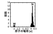
- FIG. 7 is a diagram statistically showing the charge bias of the structure in which three clusters constituting the tungsten silicide film are aggregated in the first embodiment.
- It is a cross-sectional schematic diagram of the electronic device of 2nd Embodiment. It is a figure which shows the result of having performed the time-dependent dielectric breakdown test (TDDB) under acceleration conditions as evaluation of a barrier function in 2nd Embodiment. In 2nd Embodiment, it is the figure which showed the relationship of the cumulative failure probability and failure time by a dielectric breakdown test (TDDB). In 2nd Embodiment, it is the figure which extrapolated and estimated the lifetime from the result of the dielectric breakdown test (TDDB). It is a cross-sectional schematic diagram of the electronic device of 3rd Embodiment.
- TDDB time-dependent dielectric breakdown test
- the present inventors have realized a conductive laminated body having a laminated structure in which a tungsten silicide film is laminated in contact with the conductor so that copper does not diffuse from the conductor made of an alloy containing copper or copper as a main component. It is a thing.
- the tungsten silicide film has a silicon / tungsten composition ratio of greater than 4 and 12 or less. If the composition ratio is 4 or less, the film does not have a tungsten silicon cluster structure, so the barrier function is insufficient, and if it is more than 12, copper weaves between silicon lattices in the tungsten silicide film. It moves and the barrier function becomes insufficient.
- the tungsten silicide film preferably has an amorphous structure, but may have a crystal structure.
- the thickness of the tungsten silicide film is preferably 0.3 nm or more and 10 nm or less. If the thickness is less than 0.3 nm, the barrier function is insufficient, and if it exceeds 10 nm, the parasitic resistance of the tungsten silicide film is increased.
- the tungsten silicide film prevents diffusion of copper, which is a constituent component of the conductor, from the conductor made of copper or an alloy containing copper as a main component into the surface of a metal body, a semiconductor, an insulator or the like and in a substance.
- an alloy containing copper as a main component refers to an alloy in which the component of copper is 50% or more by weight.
- the component of copper is as large as 70% by weight or more, the difference in the effect due to the presence or absence of the tungsten silicide film is remarkable.
- copper-based alloys examples include silicon copper, nickel copper, aluminum copper, manganese copper, chromium copper, copper sulfide, copper selenide, copper telluride, zirconium copper, titanium copper, gold copper, zinc copper, tin copper , Cobalt copper, tantalum copper and the like.
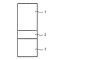
- FIG. 1 is a schematic cross-sectional view for explaining the main part of the basic structure of the conductive laminate according to the embodiment of the present invention.
- the main part of the basic structure of the conductive laminate has a laminated structure in which at least a conductor 1 made of copper or an alloy containing copper as a main component and a tungsten silicide film 2 are laminated.
- a first object is stacked in contact with the tungsten silicide film 2 on the surface of the tungsten silicide film 2 opposite to the surface in contact with the conductor 1.
- the first object is any one or more of a metal body, a semiconductor, and an insulator, and the copper alloy conductor is a substance to which copper can diffuse if adjacent.
- the method for producing a conductive laminate of the present embodiment includes the following steps.
- Step 1 A step of preparing a first object (semiconductor, metal body, insulator) as a preparation step of the conductive laminate. For example, to form an n-type MOS structure, form an n-type silicon layer, and to form a p-type MOS structure, form a silicon germanium layer.
- Step 2 A step of forming a tungsten silicide film on the first object.
- Step 3) A step of forming a conductor made of copper or an alloy containing copper as a main component on the tungsten silicide film.
- Step 4) A step of heat treatment as required.
- the formation of the tungsten silicide film in (Step 2) can be produced by chemically reacting a tungsten source gas and a silicon source gas in a gas phase. It is the same manufacturing method as that described in Patent Document 4. More specifically, the composition ratio of silicon / tungsten exceeds 4 by chemically reacting the raw material gas with the raw material gas of tungsten and the raw material gas of silicon, instead of chemically reacting the raw material gas of silicon on the substrate surface.
- a tungsten silicide film having a silicon / tungsten composition ratio of more than 4 can be produced. For example, by filling the silicon source gas in advance in a reactor maintained at 400 ° C.
- tungsten silicide film is produced.
- tungsten hexafluoride gas tungsten hexachloride gas, organic tungsten gas, etc.
- source gases for silicon silane gas, disilane gas, dichlorosilane, silicon tetrachloride and the like can be mentioned.
- step 3 the step of forming a conductor made of copper or an alloy containing copper as a main component in (step 3), the step of forming a conductor in the production of a general electrode or wiring can be appropriately used.
- the above-mentioned alloy is preferable as an alloy which has copper as a main component.
- the diffusion of these coppers into the body is caused by heat treatment above about 200 ° C.
- diffusion of copper can be prevented even through heat treatment through the tungsten silicide film. For example, even if heat treatment is performed at 600 ° C. for 30 minutes in a nitrogen atmosphere, the tungsten silicide film prevents the diffusion of copper into the object.
- FIG. 2 is a schematic cross-sectional view for explaining the structure of a semiconductor device provided with the conductive laminate of the embodiment of the present invention.
- the semiconductor device has a laminated structure in which a conductor 1 made of copper or an alloy containing copper as a main component, a tungsten silicide film 2 and a semiconductor layer 3 are laminated in this order.
- FIG. 3 is a specific example of FIG. 2 and is a cross-sectional schematic diagram of a semiconductor device having a laminated structure in which a conductor 1 made of copper or an alloy containing copper as a main component, a tungsten silicide film 2 and a semiconductor layer 3 are laminated in this order.
- the tungsten silicide film 2 has a structure in which the conductor 1 made of copper or an alloy containing copper as a main component is enclosed.
- FIG. 4 is a schematic cross-sectional view of a plane orthogonal to FIG. 3 of the structure in which the copper alloy conductor 1 is surrounded by the tungsten silicide film 2 in FIG.
- FIG. 5 shows a metal (gate) 7 and an oxide 8 between two laminated structures laminated in the order of a conductor 1 consisting of copper or an alloy mainly composed of copper, a tungsten silicide film 2 and a semiconductor layer 3.
- FIG. 6 is a schematic cross-sectional view of a semiconductor device provided with the MOS structure of the semiconductor layer 3;
- FIG. 6 shows a metal (gate) 17 and an oxide between two laminated structures laminated in the order of a conductor 1 consisting of copper or an alloy containing copper as a main component, a tungsten silicide film 2 and a silicon germanium layer 9.
- FIG. 18 is a schematic cross-sectional view of a semiconductor device provided with the MOS structure of the semiconductor layer 10;
- the tungsten silicide film of this embodiment at least one or more of silicon, germanium, a compound of silicon and germanium, and a compound of silicon and carbon are preferable.
- the compound layer of silicon and germanium preferably has a composition ratio of (germanium) / (silicon + germanium) of more than 0 and 1 or less.
- Example 1 Copper (thickness: 200 nm), tungsten silicide film (thickness: 5 nm), p + -type silicon layer (thickness: 100 nm), n-type silicon layer (thickness: 500 ⁇ m) are stacked in this order
- Example 1 of the diode was manufactured, and heat treatment at 400 ° C., 500 ° C., and 600 ° C. was performed for 30 minutes each in a nitrogen atmosphere, and diode characteristics were measured.
- Comparative Example 1 A comparative example 1 of a diode in which copper (thickness: 200 nm), p + -type silicon layer (thickness: 100 nm), and n-type silicon layer (thickness: 500 ⁇ m) are stacked in this order is fabricated. Heat treatment at 400 ° C., 500 ° C., and 600 ° C. was performed for 30 minutes each in a nitrogen atmosphere, and diode characteristics were measured.
- FIG. 7 is a diagram showing the results of comparing the diode characteristics of Example 1 and Comparative Example 1.
- FIG. 7 shows the cumulative distribution of ideal coefficients before and after heat treatment of the diodes of the example and the comparative example.
- an ideal coefficient obtained from the current-voltage characteristics of the diode was used as an index.
- those before heat treatment, after heat treatment at 400 ° C., after heat treatment at 500 ° C., and after heat treatment at 600 ° C. are respectively shown by lines efgh.
- the ideal coefficient exhibits a value close to 1 regardless of the presence or absence of the tungsten silicide film. This indicates that the diode is an ideal diode with few components of recombination current and leakage current.
- the result is largely different depending on the presence or absence of the tungsten silicide film.
- copper diffuses into the silicon layer to increase the ideal coefficient and increase the components of the recombination current and the leakage current.
- the ideal coefficient maintains a value close to 1 after heat treatment, and good diode characteristics can be obtained.
- the tungsten silicide film prevents the thermal diffusion of copper into the silicon layer. That is, the tungsten silicide film maintains the effect of the copper diffusion barrier even after the heat treatment at 600 ° C.
- the diode in which the tungsten silicide film was interposed even after the heat treatment at 600 ° C., there was no film peeling of the copper electrode, and good adhesion between the copper and the tungsten silicide film was maintained.
- the diode in which the tungsten silicide film was not interposed a change in the film structure of copper was observed visually.
- the tungsten silicide film has a feature of preventing the diffusion of copper and having high adhesion.
- the diffusion prevention mechanism of copper and the adhesion to copper were investigated.
- FIG. 8 (a) is a schematic diagram showing the stable structure of a tungsten silicon cluster consisting of one tungsten atom and 12 silicon atoms determined from the first principle calculation, and the numerical value described beside the atom is a charge. Indicates a bias.
- a material in which a large number of tungsten silicon clusters are aggregated is a tungsten silicide film.
- a positive value indicates that the charge is positively charged, and a negative value indicates that the charge is negatively charged.
- the charge moves from 12 silicon atoms to one tungsten atom, whereby the charge of silicon atoms becomes positive and the charge of tungsten atoms becomes negative, forming a polarity. .
- FIG. 8B is a schematic view showing a structure in which one copper atom is bonded to the tungsten silicon cluster in FIG. 8A obtained from the first principle calculation.
- polarity is formed between silicon atoms and copper atoms in tungsten silicon clusters. This polarity formation indicates that the silicon atom and the copper atom are strongly bonded, and the binding energy shows a large value of 3.27 eV. That is, even if copper moves in the tungsten silicide film, the tungsten silicon clusters constituting the tungsten silicide film capture the copper and the movement of the copper is inhibited.
- FIG. 9 is a diagram in which three tungsten silicon clusters shown in FIG. 8 are aggregated to statistically show the charge bias of the stable structure. This figure also shows that even in the structure in which three clusters are aggregated, there is a charge bias between silicon atoms and tungsten atoms, as in FIG. This indicates that in the case of a tungsten silicide film in which a large number of tungsten silicon clusters are aggregated, there is a charge bias between silicon atoms and tungsten atoms in the film. That is, it shows that silicon atoms and copper atoms in the tungsten silicide film are in close contact with each other with a high bonding force, and further show that the tungsten silicide film prevents the diffusion of copper.
- Second Embodiment In the second embodiment, a structure for preventing the diffusion of copper into an insulator using the conductive laminate of the present invention will be described.
- FIG. 10 is a schematic cross-sectional view of an electronic device having a laminated structure in which a conductor 1 made of copper or an alloy containing copper as a main component, a tungsten silicide film 2 and an insulator 4 are laminated in this order.
- a conductor 1 made of copper or an alloy containing copper as a main component a tungsten silicide film 2 and an insulator 4 are laminated in this order.
- an insulator the insulator normally used for an electronic device is mentioned.
- a tungsten silicide film may be provided between an electrode of the electronic device (conductor 1 composed of copper or an alloy containing copper as a main component) and an interlayer insulating film. It can.
- MOS capacitors can be configured as in the following example.
- Tungsten silicide films exhibit excellent barrier properties and also perform the functions of both conventional adhesion and barrier layers.
- the tungsten silicide film performed a sufficient function at a film thickness of 5 nm.
- the thickness of the tungsten silicide film is preferably 0.3 nm or more and 10 nm or less.
- interface scattering with a conductor made of copper or an alloy containing copper as a main component is small. That is, in the case where the barrier film is a conventional metal film, there is a problem that the conduction electrons in copper cause plasmon scattering at the interface with the barrier film to further increase resistance when the film is further miniaturized. In the case of a tungsten silicide film, there is an advantage in that there is less interface scattering because of the semiconductor.
- the tungsten silicide film has a function of barriering the diffusion of copper.
- the barrier function was examined by the following test.
- Example 2 A laminated structure in which copper (thickness: 200 nm), tungsten silicide film (thickness: 5 nm), silicon oxide film (thickness: 20 nm), and silicon layer (thickness: 500 ⁇ m) are stacked in this order Example 2 of the MOS capacitor was produced.
- Comparative Example 2 A comparative example 2 of a MOS capacitor having a laminated structure in which copper (thickness: 200 nm), silicon oxide film (thickness: 20 nm), and silicon layer (thickness: 500 ⁇ m) are stacked in this order was produced.
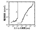
- FIG. 11 is a diagram showing the results of time-dependent dielectric breakdown test (TDDB) under accelerated conditions for Example 2 of the MOS capacitor (line B) and Comparative Example 2 of the MOS capacitor (line A).
- TDDB time-dependent dielectric breakdown test
- electric field strength of plus 5 MV / cm is continuously applied to the copper electrode in a vacuum atmosphere at 200 ° C., and current density is observed at regular intervals. This environment accelerates the diffusion of copper, and when copper diffuses into the silicon oxide film, the diffused copper serves as a leak current path, and the current density sharply increases.
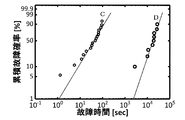
- FIG. 12 is a diagram showing the relationship between the cumulative failure probability and the failure time of the test result of FIG.
- the barrier characteristics were compared depending on the presence or absence of the tungsten silicide film, with the time when the current density reached 1 A / cm 2 as the failure time.
- the failure time of Example 2 (line D) of the MOS capacitor having the tungsten silicide film is extended by three to four orders of magnitude as compared with Comparative Example 2 (line C) of the MOS capacitor without the tungsten silicide film. .
- FIG. 13 is a diagram in which the life is extrapolated from the results of the accelerated deterioration test of the laminated structure (Example 2) in which the copper, the tungsten silicide film, the silicon oxide film, and the silicon layer are laminated in this order.
- the tungsten silicide film corresponds to a practical reliability life of 10 years or more at 100 ° C. despite the extremely thin film of 5 nm.
- FIG. 14 is a schematic cross-sectional view of an electronic device having a laminated structure in which at least a conductor 1 made of copper or an alloy containing copper as a main component, a tungsten silicide film 2 and a metal 5 are laminated in this order.
- This figure shows a stacked structure in which a tungsten silicide film 6 is further stacked in order on the metal 5.
- the tungsten silicide film (2, 6) is a structure in which the conductor 1 and the metal 5 made of copper or an alloy containing copper as a main component are surrounded.
- the electronic element of this figure is an electrode and wiring, for example.
- Examples of the metal 5 include metals conventionally used as conductive metals for electrodes and wirings.
- the metal 5 is a metal material to which copper diffuses, and the tungsten silicide film 2 has a function of a barrier layer.
- the metal 5 is preferably, for example, at least one or more of copper, tungsten, cobalt, titanium, nickel, and molybdenum.
- the electrode, insulation structure, and wiring of semiconductor devices were illustrated about the electronic device which can apply the electroconductive laminated body of this invention.
- the electronic element may be, for example, an electronic control unit, a signal input / output unit structure such as a storage unit, or a device using current, voltage, or spin.
- the electronic device of the present invention is not limited to the illustrated one.
- the conductive laminate of the present invention has a barrier layer that prevents the diffusion of copper of a conductor composed of copper or an alloy containing copper as a main component to an adjacent object, and therefore, is widely used for various electric devices and electronic parts it can.
- SYMBOLS 1 conductor which consists of an alloy which has copper or copper as a main component 2, 6 tungsten silicide film
Landscapes
- Chemical & Material Sciences (AREA)
- Organic Chemistry (AREA)
- Engineering & Computer Science (AREA)
- Inorganic Chemistry (AREA)
- Manufacturing & Machinery (AREA)
- General Chemical & Material Sciences (AREA)
- Chemical Kinetics & Catalysis (AREA)
- Materials Engineering (AREA)
- Mechanical Engineering (AREA)
- Metallurgy (AREA)
- Internal Circuitry In Semiconductor Integrated Circuit Devices (AREA)
- Electrodes Of Semiconductors (AREA)
Abstract
電極や配線等における、銅の拡散を防止するバリア機能と密着性を向上させた導電性積層体及びその製造方法、並びに電子素子を提供する。 第1の物体と、銅又は銅を主成分とする合金からなる導電体とが、タングステンシリサイド膜を介して積層された積層構造を備え、タングステンシリサイド膜のシリコン/タングステンの組成比が4より大で12以下である導電性積層体により、銅の第1の物体への拡散防止を実現する。第1の物体が、金属体、半導体、絶縁体のうちの少なくとも一つ以上である構造により、高性能の電子素子を実現する。
Description
本発明は、銅又は銅を主成分とする金属層を備える、電極や配線等に用いられる導電性積層体、及びその製造方法、並びに該導電性積層体を備える電子素子に関する。
従来、銅又は銅を主成分とする合金を用いる導電体は、銅が金属の中でも特に低抵抗であることが知られているため、半導体装置用及び電子制御装置用の電極材料や配線材料として期待されている。しかし、銅が、シリコンやゲルマニムなどの半導体層、又は酸化物や窒化物等の絶縁体層と直接に接することは、困難である。これは、銅が、半導体層や絶縁体層の表面や層中へ拡散しやすい性質を持っているためである。
そこで、電極や配線のバリア層として、窒化チタン、窒化タンタル、窒化タングステン等の窒化金属膜が適用されてきた。また、従来の銅の電極又は配線の密着層として、チタン、タンタルなどの金属膜が適用されてきた。
近年、LSIを構成するトランジスタとして、相補型金属酸化物半導体(Complementaly Metal Oxide Semiconductor(CMOS))の電界効果トランジスタが用いられている。MOSで用いられる酸化物は、ハフニウム酸化物等の金属酸化物、あるいはシリコン酸化物等の半導体酸化物であり、金属電極は、タングステン、窒化タングステン、チタン、窒化チタン、タンタル、窒化タンタル、ニッケル、コバルト、モリブデン、高キャリア濃度を有するシリコン、のうちの少なくとも一つ以上である。CMOSは、Negative(n)型MOSとPositive(p)型MOSから構成されている。n型MOSでは、通常、ソース/ドレインにおいて、金属電極とn型半導体層が接合しており、p型MOSでは、通常、ソース/ドレインにおいて、金属電極とp型半導体層が接合している。
ところで、金属とシリコンからなる遷移金属シリサイド膜は、遷移金属珪素化合物又は遷移金属珪化物とも呼ばれ、近年に研究開発が進められている。金属としての特性を利用した遷移金属シリサイド膜は、金属性シリサイド又はメタリックシリサイドと呼ばれ、耐熱性、耐酸化性、耐食性、電気伝導特性等に優れ、電極、高温構造物、耐環境用コーティング等の材料として期待される。半導体としての特性を利用した遷移金属シリサイド膜は、シリサイド半導体又はシリサイド系半導体又はセミコンダクティングシリサイドと呼ばれ、発光素子、太陽電池、熱電変換素子等の材料として期待される。また、半導体装置の技術分野では、遷移金属シリサイド膜は、シリコンを用いるLSI等のプロセスにマッチングのよい材料として知られている。
本発明者らは、先に、MSin(但し、M:遷移金属、Si:シリコン、n=7-16)に係る遷移金属シリサイド膜を提案し、該遷移金属シリサイド膜を用いた半導体装置を提案した(特許文献1、特許文献2参照)。特許文献1に係る前記遷移金属シリサイド膜MSin(但し、M:遷移金属、Si:シリコン、n=7-16)は、遷移金属とシリコンの化合物であり、遷移金属原子の周りを7個以上16個以下のSi原子が取り囲む遷移金属内包シリコンクラスターを単位構造とし、遷移金属原子の第1及び第2近接原子にSiが配置されており、次のような特徴を備えている。第1は、水素脱離による劣化の抑制であり、第2は、電界効果による電気伝導制御性と高いキャリア移動度である。また、本発明者らは、遷移金属内包シリコンクラスターを単位構造とした膜は、アモルファスシリコンに代替し薄膜トランジスタのチャネル領域に用いることができることを提案した(特許文献2参照)。
また、本発明者らは、遷移金属Mとシリコンの組成比nが7-16の範囲の金属珪素化合物薄膜を、半導体基板表面上にヘテロエピタキシャル成長させて作製した半導体コンタクト構造を提案した(特許文献3参照)。
また、本発明者らは、遷移金属の原料ガスとシリコンの原料ガスを気相中で化学反応させることにより、シリコン/遷移金属の組成比が3より大で16以下の前駆体を気相中で作製した後に、該前駆体を基板上に堆積して、シリコン/遷移金属の組成比が3より大で16以下の遷移金属シリサイド膜を該基板上に作製することを実現した(特許文献4参照)。特許文献4では、金属電極膜と半導体基板(N型Si基板)の接触界面にWSin膜を挿入したソース/ドレイン構造を持つSiのNMOSトランジスタを提案した。Si組成比nの高いWSin膜(例えば、n=8-12)を用いることにより、Si基板とWSin膜の接触界面に生じる欠陥準位を低減することができ、金属とSi基板の間で生じるエネルギー障壁の高さを制御して金属/Si基板の接触抵抗を低減することが可能となることを開示した。WSin膜を備える電極構造は、N-MOSトランジスタのみならず、P-MOSトランジスタにも有効であり、また、Siトランジスタのみならず、Geトランジスタにも有効であることを開示した。
銅が、隣接する層の表面や層中へ拡散しやすい性質を持っているため、拡散した銅が電流リークの経路となり、半導体装置および電子制御装置の性能を劣化させてしまうという問題があった。そこで、銅と、半導体層や絶縁体層との間に、銅の拡散を防止するためのバリア層を別途設ける必要がある。
従来、バリア層として窒化金属膜等を用いた場合、バリア層と半導体層が接触する界面では、大きな接触抵抗ができてしまい、この大きな接触抵抗が半導体装置や電子制御装置の性能を劣化させてしまうという問題があった。
また、バリア層と銅を密着させる必要があるが、従来のバリア層と銅には十分な密着性が無かった。そこで、密着性を向上させるために、さらに密着層が挿入されることがあった。例えば、従来の半導体装置の電極又は配線には、密着層としてタンタル、バリア層として窒化タンタルが利用されているものがある。この場合、銅、タンタル、窒化タンタルの順で積層された積層構造が採用されてきた。しかしながら、半導体装置の微細化に伴い、この電極や配線も微細化されてきたが、密着層とバリア層の厚さの薄化には限界があるので、銅の膜厚のみを小さくする必要があった。その結果、タンタルと窒化タンタルの膜厚が電極又は配線の膜厚をかなり占めるようになり、電極又は配線の寄生抵抗が高くなってしまうという問題が生じた。この問題は、半導体装置の微細化に伴い、ますます顕著になっている。
また、バリア層や密着層が金属の場合には、銅とバリア層又は密着層との界面で、伝導電子の散乱が起き、電極又は配線の高抵抗化の原因となるという問題があった。
本発明は、これらの問題を解決しようとするものであり、本発明は、銅または銅を主成分とする合金からなる導電体を構成する銅が、隣接する物体へ拡散することを防止可能な層を有する導電性積層体及びその製造方法を提供することを目的とする。また、銅または銅を主成分とする合金からなる導電体との密着性の優れた層を有する導電性積層体及びその製造方法を提供することを目的とする。銅または銅を主成分とする合金からなる導電体の、半導体との接触抵抗の低減を可能とする電子素子を提供することを目的とする。銅または銅を主成分とする合金からなる導電体の、電極乃至配線等に用いた際の寄生抵抗低減を可能とする電子素子を提供することを目的とする。
本発明は、前記目的を達成するために、以下の特徴を有するものである。
(1) 第1の物体と、銅又は銅を主成分とする合金からなる導電体とが、タングステンシリサイド膜を介して積層された積層構造を備え、前記タングステンシリサイド膜のシリコン/タングステンの組成比が4より大で12以下であることを特徴とする導電性積層体。
(2) 前記タングステンシリサイド膜の厚さは、0.3nm以上で10nm以下であることを特徴とする前記(1)に記載の導電性積層体。
(3) 前記第1の物体は、金属体、半導体、絶縁体のうちの少なくとも一つ以上であることを特徴とする前記(1)又は(2)に記載の導電性積層体。
(4) 前記半導体は、シリコン、ゲルマニウム、シリコンとゲルマニウムの化合物、シリコンとカーボンの化合物のうちの少なくとも一つ以上であることを特徴とする、前記(3)記載の導電性積層体を備える電子素子。
(5) 前記絶縁体は、シリコン酸化物、カーボン酸化物、シリコンカーボン酸化物、シロキサン系有機化合物膜、シリコン窒化物、カーボン窒化物、シリコンカーボン窒化物、金属酸化物、金属窒化物のうちの少なくとも一つ以上であることを特徴とする前記(3)に記載の導電性積層体を備える電子素子。
(6) 前記金属体は、銅、金、タングステン、コバルト、チタン、ニッケル、モリブデンのうち少なくとも一つ以上であることを特徴とする前記(3)に記載の導電性積層体を備える電子素子。
(7) タングステンの原料ガスとシリコンの原料ガスを気相中で化学反応させることにより、シリコン/タングステンの組成比が4より大で12以下の前駆体を気相中で作製した後に、該前駆体を第1の物体上に堆積して、タングステンシリサイド膜を作製する工程と、銅又は銅を主成分とする合金からなる導電体を、前記タングステンシリサイド膜上に作製する工程とを有することを特徴とする導電性積層体の製造方法。
(2) 前記タングステンシリサイド膜の厚さは、0.3nm以上で10nm以下であることを特徴とする前記(1)に記載の導電性積層体。
(3) 前記第1の物体は、金属体、半導体、絶縁体のうちの少なくとも一つ以上であることを特徴とする前記(1)又は(2)に記載の導電性積層体。
(4) 前記半導体は、シリコン、ゲルマニウム、シリコンとゲルマニウムの化合物、シリコンとカーボンの化合物のうちの少なくとも一つ以上であることを特徴とする、前記(3)記載の導電性積層体を備える電子素子。
(5) 前記絶縁体は、シリコン酸化物、カーボン酸化物、シリコンカーボン酸化物、シロキサン系有機化合物膜、シリコン窒化物、カーボン窒化物、シリコンカーボン窒化物、金属酸化物、金属窒化物のうちの少なくとも一つ以上であることを特徴とする前記(3)に記載の導電性積層体を備える電子素子。
(6) 前記金属体は、銅、金、タングステン、コバルト、チタン、ニッケル、モリブデンのうち少なくとも一つ以上であることを特徴とする前記(3)に記載の導電性積層体を備える電子素子。
(7) タングステンの原料ガスとシリコンの原料ガスを気相中で化学反応させることにより、シリコン/タングステンの組成比が4より大で12以下の前駆体を気相中で作製した後に、該前駆体を第1の物体上に堆積して、タングステンシリサイド膜を作製する工程と、銅又は銅を主成分とする合金からなる導電体を、前記タングステンシリサイド膜上に作製する工程とを有することを特徴とする導電性積層体の製造方法。
本発明では、所定の組成比のタングステンシリサイド膜を、銅又は銅を主成分とする合金からなる導電体(以下、「銅合金導電体」とも呼ぶ。)に隣接して設けることにより、銅の拡散を防止する優れたバリア特性、及び銅合金導電体との密着性向上、という効果を奏する。そのため、タングステンシリサイド膜は従来の密着層とバリア層の両方の役割を果たすことができる。
また、本発明の導電性積層体を備えた電子素子について、銅合金導電体と半導体との間にタングステンシリサイド膜を介在させる半導体装置の場合は、優れたバリア特性の効果、及び銅合金導電体と半導体層との接触抵抗低減の効果を両立させることができる。
また、本発明の導電性積層体を電極構造や配線等に用いた電子素子の場合に、タングステンシリサイド膜を介在させる場合は、高い密着性とバリア機能により、電極や配線に占める銅合金導電体の膜厚の割合を高くすることができ、銅合金導電体の電極の寄生抵抗低減の効果を奏する。
また、タングステンシリサイド膜は低い状態密度を有するため、銅合金導電体とタングステンシリサイド膜との界面での伝導電子の散乱を抑えることが可能である。その結果、電極及び配線の低抵抗化が可能である。
また、本発明によれば、銅合金導電体と半導体層との接触抵抗低減の効果を奏するため、集積回路のさらなる微細化及び性能の向上を図れる。
本発明の製造方法では、所定の組成比のタングステンシリサイド膜を堆積する工程と、銅または銅を主成分とする合金からなる導電体の形成工程を有することにより、銅が、隣接する物体へ拡散しない導電性積層体を製造することができる。
本発明の実施形態について以下説明する。
本発明者らは、銅又は銅を主成分とする合金からなる導電体から銅が拡散しないように、該導電体に接してタングステンシリサイド膜を積層した積層構造を備える導電性積層体を実現したものである。
タングステンシリサイド膜は、シリコン/タングステンの組成比が4より大で12以下である。組成比が4以下であると、膜中ではタングステンシリコンクラスター構造を有さないため、バリア機能が不十分であり、12より大であると、銅がタングステンシリサイド膜中のシリコン格子間を縫って移動してしまい、バリア機能が不十分となる。
タングステンシリサイド膜はアモルファス構造を有していることが望ましいが、結晶構造を有していてもよい。
タングステンシリサイド膜の厚さは、0.3nm以上で10nm以下であることが好ましい。0.3nmより薄いと、バリア機能が不十分であり、10nmを超えるとタングステンシリサイド膜の寄生抵抗が大きくなってしまうからである。
タングステンシリサイド膜は、銅又は銅を主成分とする合金からなる導電体から、導電体の構成成分の銅が、金属体、半導体、絶縁体等の表面及び物質内に拡散することを防止する。ここで、銅を主成分とする合金とは、銅の成分が重量比で50%以上の合金をいう。銅の成分が70重量%以上のように大である場合は、タングステンシリサイド膜の有無による効果の差が顕著である。銅を主成分とする合金として、例えば、シリコン銅、ニッケル銅、アルミニウム銅、マンガン銅、クロム銅、硫化銅、セレン化銅、テルル化銅、ジルコニウム銅、チタン銅、金銅、亜鉛銅、スズ銅、コバルト銅、タンタル銅等が挙げられる。
図1は、本発明の実施形態の導電性積層体の基本構造の主要部を説明する断面模式図である。導電性積層体の基本構造の主要部は、少なくとも、銅又は銅を主成分とする合金からなる導電体1と、タングステンシリサイド膜2とが積層された積層構造を備える。タングステンシリサイド膜2の、導電体1の接する面の反対側の面に、タングステンシリサイド膜2に接して、第1の物体が積層されている。第1の物体は、金属体、半導体、絶縁体のいずれか1つ以上であり、銅合金導電体がもし隣接したら銅が拡散されうる物質である。
本実施形態の導電性積層体の製造方法は、次の工程を備える。
(工程1) 導電性積層体の準備段階として、第1の物体(半導体、金属体、絶縁体)を準備する工程。例えば、n型MOS構造を製造するためには、n型シリコン層を、p型MOS構造を製造するためには、シリコンゲルマニウム層を形成する工程。
(工程2) 第1の物体の上にタングステンシリサイド膜を形成する工程。
(工程3) タングステンシリサイド膜の上に、銅又は銅を主成分とする合金からなる導電体を形成する工程。
(工程4) 必要に応じて熱処理する工程。
(工程1) 導電性積層体の準備段階として、第1の物体(半導体、金属体、絶縁体)を準備する工程。例えば、n型MOS構造を製造するためには、n型シリコン層を、p型MOS構造を製造するためには、シリコンゲルマニウム層を形成する工程。
(工程2) 第1の物体の上にタングステンシリサイド膜を形成する工程。
(工程3) タングステンシリサイド膜の上に、銅又は銅を主成分とする合金からなる導電体を形成する工程。
(工程4) 必要に応じて熱処理する工程。
(工程2)におけるタングステンシリサイド膜の形成は、タングステンの原料ガスとシリコンの原料ガスを気相中で化学反応させることにより作製することができる。特許文献4に記載されたと同様の製造方法である。タングステンの原料ガスとシリコンの原料ガスを基板表面で化学反応させるのではなく、原料ガスを気相中で化学反応させることによって、より具体的にいえば、シリコン/タングステンの組成比が4を超える前駆体を気相中で作製し、該前駆体を基板上へ堆積させることによって、シリコン/タングステンの組成比が4を超えるタングステンシリサイド膜を作製できる。例えば、シリコンの原料ガス同士が反応しない温度の400℃に維持した反応炉の中に、シリコンの原料ガスを予め満たしておき、その反応炉の中にタングステンの原料ガスを導入することにより、気相中でタングステンシリサイド膜の前駆体を作製する。気相中での熱的な化学反応を利用することが望ましいが、基板温度の高温化も効果的である。タングステンの原料ガスとして、六フッ化タングステンガス、六塩化タングステンガス、有機タングステンガス等が挙げられる。シリコンの原料ガスとして、シランガス、ジシランガス、ジクロロシラン、四塩化ケイ素等が挙げられる。
(工程3)における銅又は銅を主成分とする合金からなる導電体の形成工程は、通常の電極や配線の製造における導電体形成工程を適宜用いることができる。銅を主成分とする合金として、上述の合金が好ましい。
銅又は銅を主成分とする合金からなる導電体と、金属体又は半導体又は絶縁体が接している構造体について、熱処理を行うと、銅が金属体又は半導体又は絶縁体へ拡散し、金属体又は半導体又は絶縁体の特性が大きく変化してしまう。例えば、銅が金属体へ拡散すると、金属体の電気伝導率が変化する。銅が半導体へ拡散すると、半導体のバンドギャップ内に準位が形成されて、半導体のキャリアタイプやキャリア濃度が変化したり、リーク電流の原因となったりする。銅が絶縁体へ拡散すると、銅が絶縁体中でパーコレーション的に繋がってしまい、それがリーク電流の経路となり、絶縁体は電気的な絶縁性を失ってしまう。これらの銅の物体中への拡散は約200℃以上の熱処理によって起きる。一方、タングステンシリサイド膜を介することで、熱処理を行っても、銅の拡散を防止することができる。例えば、窒素雰囲気で600℃30分の熱処理を行っても、タングステンシリサイド膜が、銅の物体中への拡散を防止する。
(第1の実施形態)
本発明の第1の実施形態の導電性積層体について、図を参照して以下説明する。本実施形態では、半導体への銅の拡散を防止する構造を中心に説明する。
本発明の第1の実施形態の導電性積層体について、図を参照して以下説明する。本実施形態では、半導体への銅の拡散を防止する構造を中心に説明する。
図2は、本発明の実施形態の導電性積層体を備えた半導体装置の構造を説明する断面模式図である。半導体装置は、銅又は銅を主成分とする合金からなる導電体1、タングステンシリサイド膜2、半導体層3の順で積層された積層構造を備える。
図3は、図2の具体例であり、銅又は銅を主成分とする合金からなる導電体1、タングステンシリサイド膜2、半導体層3の順で積層された積層構造を備える半導体装置の断面模式図である。図3では、タングステンシリサイド膜2が銅又は銅を主成分とする合金からなる導電体1を囲った構造である。
図4は、図3の、タングステンシリサイド膜2で銅合金導電体1を囲った構造の、図3と直交する面の断面模式図である。
図5は、銅又は銅を主成分とする合金からなる導電体1、タングステンシリサイド膜2、半導体層3の順で積層された2つの積層構造の間に、金属(ゲート)7、酸化物8、半導体層3のMOS構造を備えた半導体装置の断面模式図である。
図6は、銅又は銅を主成分とする合金からなる導電体1、タングステンシリサイド膜2、シリコンゲルマニウム層9の順で積層された2つの積層構造の間に、金属(ゲート)17、酸化物18、半導体層10のMOS構造を備えた半導体装置の断面模式図である。
本実施形態のタングステンシリサイド膜と接する半導体として、シリコン、ゲルマニウム、シリコンとゲルマニウムの化合物、シリコンとカーボンの化合物のうちの少なくとも一つ以上が好ましい。シリコンとゲルマニウムの化合物層は、(ゲルマニウム)/(シリコン+ゲルマニウム)の組成比が0より大で1以下であることが好ましい。
〈バリア機能と熱処理の関係〉
銅とタングステンシリサイド膜の積層構造を作製した後に熱処理を行っても、タングステンシリサイド膜のバリア機能は維持される。熱処理とバリア機能について、次に示す試験により調べた。
銅とタングステンシリサイド膜の積層構造を作製した後に熱処理を行っても、タングステンシリサイド膜のバリア機能は維持される。熱処理とバリア機能について、次に示す試験により調べた。
〈実施例1〉 銅(厚さ:200nm)、タングステンシリサイド膜(厚さ:5nm)、p+型シリコン層(厚さ:100nm)、n型シリコン層(厚さ:500μm)の順で積層されたダイオードの実施例1を作製し、窒素雰囲気下で400℃、500℃、600℃の熱処理を、各々30分間行い、ダイオード特性を測定した。
〈比較例1〉 銅(厚さ:200nm)、p+型シリコン層(厚さ:100nm)、n型シリコン層(厚さ:500μm)の順で積層されたダイオードの比較例1を作製し、窒素雰囲気下で400℃、500℃、600℃の熱処理を、各々30分間行い、ダイオード特性を測定した。
図7は、実施例1と比較例1についてのダイオード特性を比較した結果を示す図である。図7は、実施例と比較例のダイオードの熱処理前後における理想係数の累積分布を示す。ここで、銅の拡散の評価には、ダイオードの電流-電圧特性から求まる理想係数を指標とした。実施例1の積層構造で、熱処理前、400℃熱処理後、500℃熱処理後、600℃熱処理後のものを、それぞれ線efghで示す。比較例1の積層構造で、熱処理前、400℃熱処理後、500℃熱処理後、600℃熱処理後のものを、それぞれ線abcdで示す。熱処理前のダイオードにおいては、タングステンシリサイド膜の有無に関係なく、理想係数が1に近い値を示す。これは、再結合電流やリーク電流の成分がほとんどなく、理想的なダイオードであることを示している。一方で熱処理後のダイオードにおいては、タングステンシリサイド膜の有無で大きく異なる結果が得られる。タングステンシリサイド膜の無いダイオードにおいては、熱処理温度の増大に伴い、銅がシリコン層中に拡散することにより、理想係数が増大し、再結合電流やリーク電流の成分が増大する。タングステンシリサイド膜のある実施例1のダイオードにおいては、熱処理後も理想係数が1に近い値を維持し、良好なダイオード特性が得られる。これは、タングステンシリサイド膜が、銅のシリコン層中への熱拡散を防止していることを示している。つまり、タングステンシリサイド膜は、600℃の熱処理後でも、銅の拡散バリアの効果を維持する。また、タングステンシリサイド膜を介在させたダイオードでは、600℃の熱処理後でも、銅電極の膜剥がれは無く、銅とタングステンシリサイド膜の良好な密着性を保った。一方、タングステンシリサイド膜を介在させないダイオードでは、目視でも銅の膜構造の変化が観測された。
〈バリア特性と密着性の評価〉
タングステンシリサイド膜は銅の拡散を防止すると共に密着性が高い特徴を有する。タングステンシリサイド膜の、銅の拡散防止機構と、銅との密着性について調べた。
タングステンシリサイド膜は銅の拡散を防止すると共に密着性が高い特徴を有する。タングステンシリサイド膜の、銅の拡散防止機構と、銅との密着性について調べた。
図8(a)は、第一原理計算から求めた1個のタングテン原子と12個のシリコン原子から成るタングステンシリコンクラスターの安定構造を示した模式図であり、原子の横に記載した数値が電荷の偏りを示している。このタングステンシリコンクラスターが多数個で凝集した物質がタングステンシリサイド膜である。プラスの値は、電荷がポジティブに帯電しており、マイナスの値は、電荷がネガティブに帯電していることを示している。このタングステンシリコンクラスターの中では12個のシリコン原子から1個のタングステン原子へ電荷が移動することにより、シリコン原子の電荷がポジティブに、タングステン原子の電荷がネガティブに偏って、極性を形成している。図8(b)は、第一原理計算から求めた、(a)図のタングステンシリコンクラスターに1個の銅原子が結合している構造を示した模式図である。銅原子がタングステンシリコンクラスターに吸着すると、タングステンシリコンクラスター内のシリコン原子と銅原子との間に極性が形成される。この極性形成は、シリコン原子と銅原子との間で強固に結合していることを示しており、この結合エネルギーは3.27eVと大きな値を示す。即ち、銅がタングステンシリサイド膜を移動しようとしても、タングステンシリサイド膜を構成しているタングステンシリコンクラスターが銅を捕獲して、銅の移動が阻害される。
図9は、図8で示したタングステンシリコンクラスターを3つ凝集させて、その安定構造の電荷の偏りを統計的に示した図である。本図は、3つのクラスターが凝集した構造においても、図8と同様に、シリコン原子とタングステン原子の間で電荷の偏りがあることを示している。これは、タングステンシリコンクラスターが多数個で凝集したタングステンシリサイド膜でも同様に、膜中でシリコン原子とタングステン原子の間で電荷の偏りがあることを示している。即ち、タングステンシリサイド膜中のシリコン原子と銅原子が高い結合力で密着することを示し、さらに、タングステンシリサイド膜が銅の拡散を防止することを示している。
上述した評価は、銅で調べたが、銅の拡散が問題となるような銅を主成分とする合金の場合も、同様に効果がある。
(第2の実施形態)
第2の実施形態では、本発明の導電性積層体を用いて絶縁体への銅の拡散を防止する構造について説明する。
第2の実施形態では、本発明の導電性積層体を用いて絶縁体への銅の拡散を防止する構造について説明する。
図10は、銅又は銅を主成分とする合金からなる導電体1、タングステンシリサイド膜2、絶縁体4の順で積層された積層構造を備える電子素子の断面模式図である。ここで、絶縁体として、電子素子に通常用いられる絶縁体が挙げられる。
本実施形態の電子素子として、半導体装置等の場合、電子素子の電極(銅又は銅を主成分とする合金からなる導電体1)と層間絶縁膜との間に、タングステンシリサイド膜を設けることができる。または、下記の例のようにMOSキャパシタを構成できる。タングステンシリサイド膜は、優れたバリア特性を示し、また従来の密着層とバリア層の両方の機能を果たす。タングステンシリサイド膜は膜厚5nmで十分な機能を果たした。タングステンシリサイド膜は膜厚が0.3nm以上で10nm以下であることが好ましい。また、銅又は銅を主成分とする合金からなる導電体との界面散乱が小さい。即ち、バリア膜が従来の金属膜である場合、より微細化する際に、銅中の伝導電子がバリア膜との界面でプラズモン散乱を起こして高抵抗化するという問題があるのに対して、タングステンシリサイド膜の場合は、半導体のため界面散乱が少ないという利点がある。
本実施形態における絶縁体として、シリコン酸化物、カーボン酸化物、シリコンカーボン酸化物、シロキサン系有機化合物膜、シリコン窒化物、カーボン窒化物、シリコンカーボン窒化物、金属酸化物、金属窒化物のうちの少なくとも一つ以上であることが好ましい。
〈バリア機能の評価〉
タングステンシリサイド膜は銅の拡散をバリアする機能を有している。バリア機能について、次に示す試験により調べた。
タングステンシリサイド膜は銅の拡散をバリアする機能を有している。バリア機能について、次に示す試験により調べた。
〈実施例2〉 銅(厚さ:200nm)、タングステンシリサイド膜(厚さ:5nm)、シリコン酸化膜(厚さ:20nm)、シリコン層(厚さ:500μm)の順で積層された積層構造のMOSキャパシタの実施例2を作製した。
〈比較例2〉 銅(厚さ:200nm)、シリコン酸化膜(厚さ:20nm)、シリコン層(厚さ:500μm)の順で積層された積層構造のMOSキャパシタの比較例2を作製した。
図11は、MOSキャパシタの実施例2(線B)とMOSキャパシタの比較例2(線A)について、加速条件下で経時絶縁破壊試験(TDDB)を行った結果を示す図である。この試験では、200℃の真空雰囲気下で、銅電極にプラス5MV/cmの電界強度を印可し続けて、電流密度を一定時間毎に観測する。この環境により、銅の拡散が加速されて、銅がシリコン酸化膜中に拡散すると、拡散した銅がリーク電流の経路となり、電流密度が急峻に増大する。
図12は、図11の試験の結果の累積故障確率と故障時間の関係を示した図である。図11の試験において、電流密度が1A/cm2に達した時間を故障時間として、タングステンシリサイド膜の有無でバリア特性を比較した。その結果、タングステンシリサイド膜を有するMOSキャパシタの実施例2(線D)が、タングステンシリサイド膜の無いMOSキャパシタの比較例2(線C)に比べて、故障時間が3桁から4桁ほど延びた。
図13は、銅、タングステンシリサイド膜、シリコン酸化膜、シリコン層の順で積層された積層構造(実施例2)の加速劣化試験の結果から、寿命を外挿予測した図である。タングステンシリサイド膜が5nmの極薄膜にも関わらず100℃で、10年間以上の実用的な信頼性寿命に相当する。
(第3の実施形態)
第3の実施形態では、本発明の導電性積層体を用いて金属体への銅の拡散を防止する構造について説明する。
第3の実施形態では、本発明の導電性積層体を用いて金属体への銅の拡散を防止する構造について説明する。
図14は、少なくとも、銅又は銅を主成分とする合金からなる導電体1、タングステンシリサイド膜2、金属5の順で積層された積層構造を備える電子素子の断面模式図である。本図は、金属5にさらにタングステンシリサイド膜6が順に積層された積層構造である。タングステンシリサイド膜(2、6)が、銅又は銅を主成分とする合金からなる導電体1及び金属5を囲った構造である。本図の電子素子は、例えば、電極や配線である。金属5として、従来から電極や配線の導電金属として用いられる金属が挙げられる。金属5は、銅が拡散するような金属材料であり、タングステンシリサイド膜2はバリア層の機能を有している。金属5は、例えば、銅、タングステン、コバルト、チタン、ニッケル、モリブデンのうち少なくとも一つ以上が好ましい。
以上、上記実施形態では、本発明の導電性積層体を適用できる電子素子について、CMOS等の半導体装置の電極や絶縁構造や配線を例示した。電子素子は、例えば、電子制御装置、記憶装置等の信号の入出力部構造、電流や電圧やスピンを利用した装置等でもよい。本発明の電子素子は、例示したものに制限されない。
なお、上記実施形態等で示した例は、発明を理解しやすくするために記載したものであり、この形態に限定されるものではない。
本発明の導電性積層体は、銅又は銅を主成分とする合金からなる導電体の銅が隣接する物体に拡散するのを防止するバリア層を有するので、各種電気装置、電子部品に幅広く利用できる。
1 銅又は銅を主成分とする合金からなる導電体
2、6 タングステンシリサイド膜
3、10 半導体層
4 絶縁体
5 金属
7、17 金属(ゲート)
8、18 酸化物
9 シリコンゲルマニウム層
2、6 タングステンシリサイド膜
3、10 半導体層
4 絶縁体
5 金属
7、17 金属(ゲート)
8、18 酸化物
9 シリコンゲルマニウム層
Claims (7)
- 第1の物体と、銅又は銅を主成分とする合金からなる導電体とが、タングステンシリサイド膜を介して積層された積層構造を備え、前記タングステンシリサイド膜のシリコン/タングステンの組成比が4より大で12以下であることを特徴とする導電性積層体。
- 前記タングステンシリサイド膜の厚さは、0.3nm以上で10nm以下であることを特徴とする請求項1に記載の導電性積層体。
- 前記第1の物体は、金属体、半導体、絶縁体のうちの少なくとも一つ以上であることを特徴とする請求項1又は2に記載の導電性積層体。
- 前記半導体は、シリコン、ゲルマニウム、シリコンとゲルマニウムの化合物、シリコンとカーボンの化合物のうちの少なくとも一つ以上であることを特徴とする、請求項3記載の導電性積層体を備える電子素子。
- 前記絶縁体は、シリコン酸化物、カーボン酸化物、シリコンカーボン酸化物、シロキサン系有機化合物膜、シリコン窒化物、カーボン窒化物、シリコンカーボン窒化物、金属酸化物、金属窒化物のうちの少なくとも一つ以上であることを特徴とする請求項3に記載の導電性積層体を備える電子素子。
- 前記金属体は、銅、金、タングステン、コバルト、チタン、ニッケル、モリブデンのうち少なくとも一つ以上であることを特徴とする請求項3に記載の導電性積層体を備える電子素子。
- タングステンの原料ガスとシリコンの原料ガスを気相中で化学反応させることにより、シリコン/タングステンの組成比が4より大で12以下の前駆体を気相中で作製した後に、該前駆体を第1の物体上に堆積して、タングステンシリサイド膜を作製する工程と、
銅又は銅を主成分とする合金からなる導電体を、前記タングステンシリサイド膜上に作製する工程とを有することを特徴とする導電性積層体の製造方法。
Priority Applications (1)
| Application Number | Priority Date | Filing Date | Title |
|---|---|---|---|
| JP2019552744A JP6893372B2 (ja) | 2017-11-09 | 2018-10-31 | 導電性積層体及び電子素子 |
Applications Claiming Priority (2)
| Application Number | Priority Date | Filing Date | Title |
|---|---|---|---|
| JP2017216449 | 2017-11-09 | ||
| JP2017-216449 | 2017-11-09 |
Publications (1)
| Publication Number | Publication Date |
|---|---|
| WO2019093207A1 true WO2019093207A1 (ja) | 2019-05-16 |
Family
ID=66437758
Family Applications (1)
| Application Number | Title | Priority Date | Filing Date |
|---|---|---|---|
| PCT/JP2018/040556 Ceased WO2019093207A1 (ja) | 2017-11-09 | 2018-10-31 | 導電性積層体及び電子素子 |
Country Status (2)
| Country | Link |
|---|---|
| JP (1) | JP6893372B2 (ja) |
| WO (1) | WO2019093207A1 (ja) |
Citations (5)
| Publication number | Priority date | Publication date | Assignee | Title |
|---|---|---|---|---|
| JP2000003884A (ja) * | 1998-06-15 | 2000-01-07 | Toshiba Corp | 半導体装置およびその製造方法 |
| JP2000040675A (ja) * | 1998-07-23 | 2000-02-08 | Sony Corp | 半導体装置の製造方法およびそれによる半導体装置 |
| JP2009246379A (ja) * | 1997-11-05 | 2009-10-22 | Tokyo Electron Ltd | 半導体集積装置の製造方法 |
| WO2013133060A1 (ja) * | 2012-03-06 | 2013-09-12 | 独立行政法人産業技術総合研究所 | 半導体コンタクト構造及びその形成方法 |
| JP2016211038A (ja) * | 2015-05-08 | 2016-12-15 | 国立研究開発法人産業技術総合研究所 | 遷移金属シリサイド膜、その製造方法及び製造装置並びに半導体装置 |
-
2018
- 2018-10-31 WO PCT/JP2018/040556 patent/WO2019093207A1/ja not_active Ceased
- 2018-10-31 JP JP2019552744A patent/JP6893372B2/ja active Active
Patent Citations (5)
| Publication number | Priority date | Publication date | Assignee | Title |
|---|---|---|---|---|
| JP2009246379A (ja) * | 1997-11-05 | 2009-10-22 | Tokyo Electron Ltd | 半導体集積装置の製造方法 |
| JP2000003884A (ja) * | 1998-06-15 | 2000-01-07 | Toshiba Corp | 半導体装置およびその製造方法 |
| JP2000040675A (ja) * | 1998-07-23 | 2000-02-08 | Sony Corp | 半導体装置の製造方法およびそれによる半導体装置 |
| WO2013133060A1 (ja) * | 2012-03-06 | 2013-09-12 | 独立行政法人産業技術総合研究所 | 半導体コンタクト構造及びその形成方法 |
| JP2016211038A (ja) * | 2015-05-08 | 2016-12-15 | 国立研究開発法人産業技術総合研究所 | 遷移金属シリサイド膜、その製造方法及び製造装置並びに半導体装置 |
Also Published As
| Publication number | Publication date |
|---|---|
| JPWO2019093207A1 (ja) | 2020-12-03 |
| JP6893372B2 (ja) | 2021-06-23 |
Similar Documents
| Publication | Publication Date | Title |
|---|---|---|
| JP7833062B2 (ja) | 撮像装置 | |
| KR102434699B1 (ko) | 확산방지층을 포함하는 다층구조체 및 이를 구비하는 소자 | |
| US9530893B2 (en) | Semiconductor device, measurement apparatus, and measurement method of relative permittivity | |
| CN110660674A (zh) | 制造二维材料结构的方法 | |
| TW201430958A (zh) | 於銅基導體結構上形成石墨襯墊及/或蓋罩層之方法 | |
| CN108369964A (zh) | 层叠体 | |
| JP2016072498A (ja) | 半導体装置 | |
| US20150243562A1 (en) | Semiconductor device and manufacturing method thereof | |
| JP2026075098A (ja) | 半導体装置 | |
| WO2012121415A1 (ja) | 酸化物半導体用電極、その形成方法、及びその電極を備えた酸化物半導体装置 | |
| JP6240017B2 (ja) | 半導体装置及びその製造方法 | |
| Kim et al. | Unveiling the role of Al2O3 interlayer in indium–gallium–zinc–oxide transistors | |
| TWI515912B (zh) | 半導體元件 | |
| JP6896305B2 (ja) | 半導体装置及びその製造方法 | |
| JP2019117940A (ja) | 酸化物半導体薄膜、薄膜トランジスタ及びスパッタリングターゲット | |
| JP6893372B2 (ja) | 導電性積層体及び電子素子 | |
| CN105793969A (zh) | 半导体装置和半导体装置的制造方法 | |
| Wang et al. | Evolution of enhanced performance of a-IGZO TFTs with Cu/Al-based contacts | |
| JP6120340B2 (ja) | 異種材料接合を有する半導体デバイス | |
| JP2008053554A (ja) | 電子デバイスとその製造方法 | |
| JP6015992B2 (ja) | 水素化アモルファスシリコン系膜を有する記憶素子 | |
| KR20150128322A (ko) | 박막 트랜지스터 제조 방법 | |
| US20250040209A1 (en) | Artificial double-layer two-dimensional material and method of manufacturing same | |
| WO2019107043A1 (ja) | 酸化物半導体薄膜、薄膜トランジスタ及びスパッタリングターゲット | |
| Okada et al. | Cluster-preforming-deposited amorphous WSi n (n= 12) insertion film of low SBH and high diffusion barrier for direct Cu contact |
Legal Events
| Date | Code | Title | Description |
|---|---|---|---|
| 121 | Ep: the epo has been informed by wipo that ep was designated in this application |
Ref document number: 18875031 Country of ref document: EP Kind code of ref document: A1 |
|
| ENP | Entry into the national phase |
Ref document number: 2019552744 Country of ref document: JP Kind code of ref document: A |
|
| NENP | Non-entry into the national phase |
Ref country code: DE |
|
| 122 | Ep: pct application non-entry in european phase |
Ref document number: 18875031 Country of ref document: EP Kind code of ref document: A1 |