WO2019087551A1 - 電気コネクタ装置 - Google Patents
電気コネクタ装置 Download PDFInfo
- Publication number
- WO2019087551A1 WO2019087551A1 PCT/JP2018/031863 JP2018031863W WO2019087551A1 WO 2019087551 A1 WO2019087551 A1 WO 2019087551A1 JP 2018031863 W JP2018031863 W JP 2018031863W WO 2019087551 A1 WO2019087551 A1 WO 2019087551A1
- Authority
- WO
- WIPO (PCT)
- Prior art keywords
- connector
- width direction
- shield shell
- substrate
- contact
- Prior art date
- Legal status (The legal status is an assumption and is not a legal conclusion. Google has not performed a legal analysis and makes no representation as to the accuracy of the status listed.)
- Ceased
Links
Images


Classifications
-
- H—ELECTRICITY
- H01—ELECTRIC ELEMENTS
- H01R—ELECTRICALLY-CONDUCTIVE CONNECTIONS; STRUCTURAL ASSOCIATIONS OF A PLURALITY OF MUTUALLY-INSULATED ELECTRICAL CONNECTING ELEMENTS; COUPLING DEVICES; CURRENT COLLECTORS
- H01R12/00—Structural associations of a plurality of mutually-insulated electrical connecting elements, specially adapted for printed circuits, e.g. printed circuit boards [PCB], flat or ribbon cables, or like generally planar structures, e.g. terminal strips, terminal blocks; Coupling devices specially adapted for printed circuits, flat or ribbon cables, or like generally planar structures; Terminals specially adapted for contact with, or insertion into, printed circuits, flat or ribbon cables, or like generally planar structures
- H01R12/70—Coupling devices
- H01R12/71—Coupling devices for rigid printing circuits or like structures
- H01R12/72—Coupling devices for rigid printing circuits or like structures coupling with the edge of the rigid printed circuits or like structures
- H01R12/73—Coupling devices for rigid printing circuits or like structures coupling with the edge of the rigid printed circuits or like structures connecting to other rigid printed circuits or like structures
-
- H—ELECTRICITY
- H01—ELECTRIC ELEMENTS
- H01R—ELECTRICALLY-CONDUCTIVE CONNECTIONS; STRUCTURAL ASSOCIATIONS OF A PLURALITY OF MUTUALLY-INSULATED ELECTRICAL CONNECTING ELEMENTS; COUPLING DEVICES; CURRENT COLLECTORS
- H01R13/00—Details of coupling devices of the kinds covered by groups H01R12/70 or H01R24/00 - H01R33/00
- H01R13/648—Protective earth or shield arrangements on coupling devices, e.g. anti-static shielding
- H01R13/658—High frequency shielding arrangements, e.g. against EMI [Electro-Magnetic Interference] or EMP [Electro-Magnetic Pulse]
- H01R13/6581—Shield structure
- H01R13/6582—Shield structure with resilient means for engaging mating connector
-
- H—ELECTRICITY
- H01—ELECTRIC ELEMENTS
- H01R—ELECTRICALLY-CONDUCTIVE CONNECTIONS; STRUCTURAL ASSOCIATIONS OF A PLURALITY OF MUTUALLY-INSULATED ELECTRICAL CONNECTING ELEMENTS; COUPLING DEVICES; CURRENT COLLECTORS
- H01R12/00—Structural associations of a plurality of mutually-insulated electrical connecting elements, specially adapted for printed circuits, e.g. printed circuit boards [PCB], flat or ribbon cables, or like generally planar structures, e.g. terminal strips, terminal blocks; Coupling devices specially adapted for printed circuits, flat or ribbon cables, or like generally planar structures; Terminals specially adapted for contact with, or insertion into, printed circuits, flat or ribbon cables, or like generally planar structures
- H01R12/70—Coupling devices
- H01R12/71—Coupling devices for rigid printing circuits or like structures
-
- H—ELECTRICITY
- H01—ELECTRIC ELEMENTS
- H01R—ELECTRICALLY-CONDUCTIVE CONNECTIONS; STRUCTURAL ASSOCIATIONS OF A PLURALITY OF MUTUALLY-INSULATED ELECTRICAL CONNECTING ELEMENTS; COUPLING DEVICES; CURRENT COLLECTORS
- H01R13/00—Details of coupling devices of the kinds covered by groups H01R12/70 or H01R24/00 - H01R33/00
- H01R13/02—Contact members
- H01R13/10—Sockets for co-operation with pins or blades
- H01R13/11—Resilient sockets
- H01R13/115—U-shaped sockets having inwardly bent legs, e.g. spade type
-
- H—ELECTRICITY
- H01—ELECTRIC ELEMENTS
- H01R—ELECTRICALLY-CONDUCTIVE CONNECTIONS; STRUCTURAL ASSOCIATIONS OF A PLURALITY OF MUTUALLY-INSULATED ELECTRICAL CONNECTING ELEMENTS; COUPLING DEVICES; CURRENT COLLECTORS
- H01R13/00—Details of coupling devices of the kinds covered by groups H01R12/70 or H01R24/00 - H01R33/00
- H01R13/648—Protective earth or shield arrangements on coupling devices, e.g. anti-static shielding
- H01R13/658—High frequency shielding arrangements, e.g. against EMI [Electro-Magnetic Interference] or EMP [Electro-Magnetic Pulse]
- H01R13/6581—Shield structure
-
- H—ELECTRICITY
- H01—ELECTRIC ELEMENTS
- H01R—ELECTRICALLY-CONDUCTIVE CONNECTIONS; STRUCTURAL ASSOCIATIONS OF A PLURALITY OF MUTUALLY-INSULATED ELECTRICAL CONNECTING ELEMENTS; COUPLING DEVICES; CURRENT COLLECTORS
- H01R13/00—Details of coupling devices of the kinds covered by groups H01R12/70 or H01R24/00 - H01R33/00
- H01R13/648—Protective earth or shield arrangements on coupling devices, e.g. anti-static shielding
- H01R13/658—High frequency shielding arrangements, e.g. against EMI [Electro-Magnetic Interference] or EMP [Electro-Magnetic Pulse]
- H01R13/6591—Specific features or arrangements of connection of shield to conductive members
- H01R13/6594—Specific features or arrangements of connection of shield to conductive members the shield being mounted on a PCB and connected to conductive members
Definitions
- the present invention relates to an electrical connector device.
- an electrical connector device for substrate connection called a stacking connector or the like is widely adopted.
- the substrate connecting electrical connector device for example, the second connector (plug connector) to which the second wiring board is connected is disposed above the first connector (or receptacle connector) to which the first wiring board is connected. And the second connector on the upper side is pushed down toward the first connector on the lower side from such an upper and lower opposed state, thereby fitting the two electrical connectors to each other.
- a structure is used in which the first and second wiring boards are electrically connected to each other.
- the electrical connector device tends to be elongated in the connector width direction.
- the shield shell provided in such an elongated electrical connector device is liable to be bent or deformed by being formed into an elongated structure, to obtain a planned shielding function or impedance characteristic. May not be
- Patent No. 6117415 gazette
- an object of the present invention is to provide an electrical connector device for connecting to a substrate which can easily achieve miniaturization in the connector width direction in a structure in which a shield shell is disposed at an outward position in the connector width direction with respect to contact members. To provide.
- the invention according to claim 1 comprises a first connector and a second connector which are brought into a fitted state in a state of being mounted on the main surfaces of the first and second wiring boards, respectively.
- First and second contact members made of a conductive member for signal connection and the first and second contact members provided on the first and second insulating housings provided in the first and second connectors, respectively
- Conductive first and second shield shells having a predetermined board width in the connector width direction are attached at an outward position in the connector width direction with respect to the first and second shield shells
- First and second substrate connection portions are electrically connected to first and second ground conductive paths provided on the first and second wiring substrates, and the first connector and the 2 connection And when the first shield shell is in the connector width direction and the second shield shell is in the connector width direction with the inward end surface facing each other in the connector width direction.
- the first substrate connection portion protrudes outward from the outer end surface of the first shield shell in the connector width direction, and the first connector and the second connector are provided. And the inboard end face in the connector width direction at the first board connection portion is disposed within the range of the plate width of the second shield shell in the connector width direction.
- the first shield shell is disposed inward in the connector width direction with respect to the first substrate connection portion, both connectors are engaged.
- the second shield shell disposed outside the first shield shell is disposed further inside the connector than in the conventional case, and the first substrate connection portion of the first shield shell and the first contact member
- the electric connector device as a whole is miniaturized in the connector width direction while securing the distance between the signal connection portion and the connector in the connector width direction.
- the first substrate connecting portion protrudes from the outer end surface of the first shield shell outward in the connector width direction, and the first substrate connecting portion from the step portion It is desirable to have the connection piece part which protrudes toward the main surface of 1 wiring board.
- the entire first shield shell is the first shield shell by the amount that the connection piece portion of the first substrate connection portion protrudes toward the main surface of the first wiring substrate.
- the first shield shell is less likely to interfere with the signal transmission conductive path of the first contact member disposed inward of the first shield shell, while being kept apart from the main surface of the first wiring board. It becomes a state. As a result, it becomes possible to bring the first shield shell close to the signal transmission conductive path, and the signal transmission to which the first contact member is connected is the ground conductive path to which the first substrate connection portion of the first shield shell is connected. Further miniaturization can be achieved by approaching the conductive path in the connector width direction.
- the first substrate connection portion can be spaced apart from the outer end surface in the connector width direction of the first housing in the connector width direction.
- the first housing is provided at an outer end face in the connector width direction with the first shield shell at a portion opposed to the first contact member in the connector width direction. It is desirable to have an air gap which is spaced inward from the connector in the connector width direction.
- connection state of the first contact member and the like can be observed through the air gap, and the impedance characteristics can be improved by adjusting the size of the air gap. It becomes adjustable to a suitable state.
- a plurality of the first and second contact members are disposed at predetermined intervals in the connector longitudinal direction orthogonal to the connector width direction, and the connector In the longitudinal direction, the first substrate connection portion may be disposed between the adjacent first contact members.
- the first and second contact members are electrically connected to first and second signal transmission conductive paths provided on the first and second wiring boards. That at least a part of the first and second signal transmission conductive paths are disposed in a state of being opposed to the first and second ground conductive paths in the connector width direction. It is possible.
- the first shield shell in the invention according to claim 1 extends along the longitudinal direction of the connector, and both ends in the extending direction of the first shield shell
- an engagement piece fixed to a part of the first housing is provided in the middle portion.
- the first shield shell is firmly fixed to the first housing through the engagement piece, and there is a risk of deformation of the first shield shell. Since the gap is eliminated, the size of the gap can be kept constant, and a stable shielding function can be obtained.
- the substrate connecting electrical connector device can easily achieve miniaturization in the connector width direction in the structure in which the shield shell is disposed at the outward position in the connector width direction with respect to the contact member. it can.
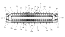
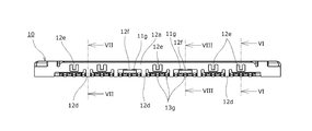
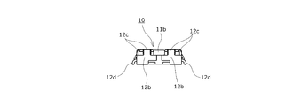
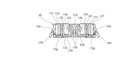
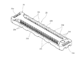
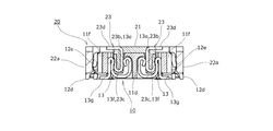
- FIG. 1 It is an appearance perspective explanatory view which expressed the 1st connector (receptacle connector) concerning one embodiment of the present invention from the upper part side. It is an appearance perspective explanatory view showing the state where the 1st connector (receptacle connector) concerning one embodiment of the present invention shown in Drawing 1 was turned upside down. It is plane explanatory drawing which represented the 1st connector (receptacle connector) concerning one Embodiment of this invention shown by FIG.1 and FIG.2. It is front explanatory drawing showing the 1st connector (receptacle connector) concerning one Embodiment of this invention shown by FIGS. 1-3. It is side explanatory drawing showing the 1st connector (receptacle connector) concerning one Embodiment of this invention shown by FIGS. 1-4. FIG.
- FIG. 10 is an exploded perspective view showing a first connector (a receptacle connector) according to the embodiment of the present invention shown in FIGS. 1 to 8;
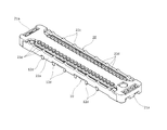
- FIG. 10 is an external perspective view showing a second connector (plug connector) according to an embodiment of the present invention fitted to the first connector (receptacle connector) shown in FIGS. 1 to 9 as viewed from above.
- FIG. 13 is a front view showing a second connector (plug connector) according to the embodiment of the present invention shown in FIGS. 10 to 12;
- FIG. 14 is a side view showing a second connector (plug connector) according to the embodiment of the present invention shown in FIGS. 10 to 13;
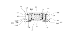
- FIG. 13 is an enlarged cross-sectional explanatory view taken along the line XV-XV in FIG. 12;
- FIG. 13 is an enlarged cross-sectional explanatory view taken along line XVI-XVI in FIG. 12;
- FIG. 17 is an external perspective view showing the second connector (plug connector) according to the embodiment of the present invention shown in FIGS. 10 to 16 in an exploded manner. It is an appearance perspective explanatory view showing the state where the 1st and 2nd connectors concerning one embodiment of the present invention were made to fit with the 2nd connector upwards from the upper part.
- FIG. 19 is an external perspective explanatory view showing a state in which the fitting state of the first and second connectors shown in FIG. 18 is vertically inverted;
- FIG. 20 is an explanatory plan view showing a fitting state of the first and second connectors shown in FIG. 18 and FIG.
- FIG. 19 It is front explanatory drawing showing the fitting state of the 1st and 2nd connectors shown by FIG.18 and FIG.19.
- FIG. 20 is an explanatory side view showing a fitted state of the first and second connectors shown in FIG. 18 and FIG. 19;
- FIG. 22 is an enlarged explanatory cross-sectional view of the semiconductor device taken along with the wiring board along the line XXIII-XXIII in FIG. 21.
- FIG. 22 is an enlarged explanatory cross-sectional view of the semiconductor device taken along with the wiring board along the line XXIV in FIG. 21.
- It is an appearance perspective explanatory view showing an example of structure of a wiring board in which a 1st connector (receptacle connector) is mounted.
- It is an appearance perspective explanatory view showing an example of structure of a wiring board in which a 2nd connector (plug connector) is mounted.
- the electrical connector apparatus for substrate connection according to the embodiment of the present invention shown in FIGS. 1 to 24 electrically connects wiring boards disposed in various electronic devices such as, for example, a smartphone or a tablet computer.
- the receptacle connector 10 as the first connector shown in FIGS. 1 to 9 is used to connect, and the plug connector 20 as the second connector shown in FIGS. 10 to 17. It is done. Then, the receptacle connector (first connector) 10 is mounted on the main surface of the first wiring board P1 shown, for example, in FIG.
- the plug connector (second connector) 20 is, for example,
- the first and second electrical connectors 10 and 20 mounted on the main surface of the second wiring board P2 shown in FIG. 26 by solder bonding or the like and in the mounted state are mutually wiring boards
- the first and second wiring boards P1 and P2 described above are electrically connected via the two electrical connectors 10 and 20 by performing the fitting operation after the main surfaces of the two are arranged so as to face each other. It will be.
- the fitting direction of the receptacle connector (first connector) 10 and the plug connector (second connector) 20 is referred to as “vertical direction”, and the receptacle connector 10 disposed at the lower position in the vertical direction 18 to 24 by, for example, pressing the plug connector 20 downward from the state in which the two electrical connectors 10 and 20 are aligned from the upper and lower facing states in which the plug connector 20 is disposed at the upper position. As shown in FIG. 1, the two electrical connectors 10, 20 are engaged with each other.
- the plug connector (second connector) 20 is pulled upward with an appropriate force from the above-mentioned fitted state, whereby the plug connector 20 is pulled upward from the lower receptacle connector (first connector) 10 It is made to be configured.
- the operation of fitting and removing the plug connector (second connector) 20 with respect to the receptacle connector (first connector) 10 is not limited to being performed by the hand of the operator, and a predetermined jig may be used. It can also be done automatically by using a machine.
- the plug connector (second connector) 20 disposed above the receptacle connector (first connector) 10 disposed below is provided.
- the second state is a state before the inversion, that is, the second one disposed in the lower side. A description will be given in a state where the plug connector 20 is mounted from above to the wiring substrate P2.
- the receptacle connector (first connector) 10 and the plug connector (second connector) 20 constituting such a substrate connecting electrical connector device each have a first housing 11 and a second housing 21 extending in a slender shape.
- the first housing 11 and the second housing 21 are formed, for example, by molding using a resin material such as insulating plastic, but along the longitudinal direction of the first housing 11 and the second housing 21.
- a large number of first contact members 13 and second contact members 23 formed of conductive members for signal connection are arranged at a predetermined pitch.
- the longitudinal direction of the first housing 11 and the second housing 21 which are the arrangement direction of the first contact member 13 and the second contact member 23 is hereinafter referred to as “connector longitudinal direction”, and the “connector longitudinal direction” and “the connector longitudinal direction”
- the short direction orthogonal to the up and down direction is referred to as the “connector width direction”.
- first housing 11 and the second housing 21 is, as particularly shown in FIGS. 9 and 17, at both end portions in the longitudinal direction (connector longitudinal direction) of the first housing 11 and the second housing 21. It has proximal end portions 11a, 11a and 21a, 21a.
- a central convex portion 11b is provided so as to integrally bridge the central portions in the connector width direction of the proximal end portions 11a and 11a in the connector longitudinal direction.
- a central recess 21b is provided so as to integrally bridge the central portions in the connector width direction of the base end portions 21a, 21a in the connector longitudinal direction.
- the base end portions 11a, 11a and 21a, 21a of the first housing 11 and the second housing 21 are disposed in an arrangement relationship opposing in the connector longitudinal direction via the central convex portion 11b and the central concave portion 21b.
- the first shield shell 12 and the second shield shell 22 are attached such that both ends in the connector width direction at the base end portions 11a and 11a and the base end portions 21a and 21a are bridged in the connector longitudinal direction.
- the first shield shell 12 and the second shield shell 22 are formed of a bent structure of a conductive member made of a thin plate-like metal member or the like, and shields against the first contact member 13 and the second contact member 23 described later.
- the outer portions of the first housing 11 and the second housing 21 are mounted in a substantially rectangular rectangular shape sandwiching from both sides in the connector longitudinal direction and the connector width direction.
- the first shield shell 12 attached to the receptacle connector (first connector) 10 at this time is fixed to the first housing 11 by press fitting from above, while the first shield shell 12 is fixed to the plug connector (second connector) 20.
- the mounted second shield shell 22 is fixed to the second housing 21 by press-fitting or insert molding from above.
- contact mounting grooves 11c having a concave shape are arranged in parallel along the longitudinal direction of the connector at a constant interval.
- contact attachment grooves (not shown) are also provided in parallel so as to be parallel to each other at a constant interval along the longitudinal direction of the connector.
- the first contact member 13 and the second contact member 23 are attached to the contact attachment grooves 11c and the like by press-fitting or insert molding, respectively. A plurality of these first contact members 13 and second contact members 23 are arranged at regular intervals along the longitudinal direction of the connector.
- the overall configurations of the receptacle connector (first connector) 10 and the plug connector (second connector) 20 are as outlined above, but the detailed configuration and arrangement relationship of each part will be described below.
- the first contact member 13 attached to the first housing 11 of the receptacle connector (first connector) 10 by press fitting, and the second contact 21 of the plug connector (second connector) 20 attached by insert molding
- the two contact members 23 are arranged to form, for each of the electrical connectors 10 and 20, two rows of electrode rows extending substantially in parallel along the longitudinal direction of the connector.
- the first contact members 13, 13 and the second contact members 23, 23 constituting the two electrode rows are arranged to face each other symmetrically in the connector width direction.
- the first contact members 13 and 13 and the second contact members 23 and 23 having the symmetrical arrangement relationship are the same without distinction.
- the central convex portion 11b of the first housing 11 to which the first contact member 13 of the receptacle connector (first connector) 10 is attached is first described above, as particularly shown in FIG.
- a partition plate 11d projecting upward from the bottom plate is provided so as to extend in the form of a strip along the longitudinal direction of the connector in a portion between the two electrode rows, ie, in the central portion in the connector width direction. It is done.
- the partition plate 11d constitutes a groove bottom portion in the connector width direction of the above-mentioned contact attachment groove 11c, and the partition plate 11d and the longitudinal direction provided on both sides in the connector width direction of the partition plate 11d.
- the pair of first contact members 13, 13 constituting the electrode rows on both sides face each other in a symmetrical manner in the connector width direction. It is arranged.
- Each of the first contact members 13 is formed of a metal strip plate member bent so as to extend in a curved shape outward from the central portion of the connector in the connector width direction,
- the contact mounting groove 11c is attached by press-fitting from below.
- the fitting concave portion 13 a bent to extend in a substantially U shape is formed to be recessed in a portion near the center of the connector near the partition plate 11 d described above.
- a part of the second contact member 23 of the plug connector (second connector) 20 which is the mating fitting body is inserted from above into the inner space of the fitting recess 13a.
- the fitting recess 13a of the first contact member 13 extending in a substantially U shape is an outwardly rising upper edge rising upward from both sides of the bottom portion 13b extending in the connector width direction. It has a portion 13c and an inner rising edge portion 13d.
- the outwardly rising upper side portion 13c disposed outward in the connector width direction is on the lower side with respect to the contact attachment groove 11c recessed in the above-described longitudinal side wall portion 11a. It is made to be in a fixed state by being press-fit from.
- the upper side portion 13d extends in the same manner as the cantilever.
- the inner rising upper side portion 13d is disposed to be close to the partition plate 11d closer to the center of the connector, and is opposed in the connector width direction to the outer rising upper side portion 13c which is fixed as described above. It can be elastically displaced in the direction of
- the upper end portion of the inner rising upper side portion 13d disposed on the center side of the connector is bent and formed so as to protrude in a curved shape toward the inner space of the fitting recess 13a described above.
- an inward contact portion 13e is formed in a convex shape at a portion that protrudes into the inward space of the fitting recess 13a.
- the outwardly rising upper side portion 13c disposed on the connector outer side is inserted into the inside of the contact attachment groove 11c provided in the longitudinal side wall portion 11a as described above, and the inward space of the fitting recess 13a
- the outer contact portion 13f is formed in a convex shape at a portion facing the lower end. As described above, when the part of the second contact member 23 of the plug connector (second connector) 20 is inserted into the inward space of the fitting recess 13a, the outer contact portion 13f is the second contact. An electrical connection is made in contact with a part of the member 23. This point will also be described in detail later.
- the first contact member 13 of the receptacle connector (first connector) 10 is provided with two inward contact portions 13e and outward contact portions 13f for each fitting recess 13a of each first contact member 13 Signal to the second contact member 23 of the plug connector (second connector) 20 via the inner contact portion 13e and the outer contact portion 13f provided for each first contact member 13. It is configured to be transmitted.
- the outwardly rising upper side portion 13c of the first contact member 13 is raised to the upper surface position of the receptacle connector (first connector) 10 from the above-described bottom side portion 13b and protrudes toward the connector outward side
- the first contact connection portion (signal connection portion) is bent in a reverse U shape so as to be turned backward downward and is bent toward the outer side of the connector at the lower surface position of the receptacle connector 10 again. ) 13g has been made.
- the first contact connecting portion 13g extends substantially horizontally outward in the connector width direction, and is shown in FIG. 25 when the receptacle connector 10 is mounted on the first wiring board P1. It is soldered to the signal transmission conductive path (signal pad) P1a on the first wiring board P1.
- the solder bonding of the first contact connection portion 13g is collectively performed to all the first contact connection portions 13g using a long solder material.
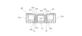
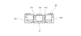
- the central recess 21b of the second housing 21 in the plug connector (second connector) 20 extends substantially parallel along the connector longitudinal direction (arrangement direction of the second contacts 23) It has a pair of longitudinal side wall parts 21d and 21d.
- a plurality of contact attachment grooves (not shown) in the form of concave grooves are arranged at regular intervals along the longitudinal direction of the connector in their respective longitudinal side wall portions 21d.
- the second contact member 23 is attached by insert molding so as to constitute two electrode rows.
- the second contact members 23 constituting the two electrode rows are arranged to face each other symmetrically in the connector width direction.
- the central recess 21b of the second housing 21 to which the second contact member 23 is attached is, as particularly shown in FIGS. 15 and 16, between the two electrode rows described above.
- the portions, that is, the portions between the longitudinal side walls 21d on both sides are formed to form a concave space extending in the longitudinal direction of the connector, and each longitudinal side wall 21d is surrounded from the outer periphery in the cross section.
- the second contact member 23 is attached.
- the pair of second contact members 23, 23 constituting the electrode rows on both sides are disposed to face each other in a symmetrical manner in the connector width direction.
- each of the second contact members 23 a portion projecting upward with a U-shaped cross section is formed on the fitting convex portion 23 a.
- Those fitting projections 23a are inserted from above into the fitting recesses 13a provided in the first contact member 13 of the receptacle connector (first connector) 10 which is the mating fitting body, and the first contact member 13 is inserted. Is elastically displaced to be received inside the fitting recess 13a.
- the above-described U-shaped fitting convex portion 23a of the second contact member 23 has an inner wall surface near the center of the connector extending substantially in parallel in the vertical direction and an outer wall surface near the outer surface of the connector.
- the inner contact portion 23b and the outer contact portion 23c are formed, for example, in a concave shape on the inner and outer wall surfaces of the connector.
- the plug connector (a first connector member) is provided with a plug connector (a first connector) in which the two electrical connectors 10 and 20 are fitted to each other. 2)
- the fitting projection 23a of the second contact member 23 provided in the connector 20 is inserted, the inner contact portion 23b and the outer contact portion 23c of the plug connector 20 are included in the receptacle connector 10 described above. Signal transmission is performed by electrically connecting the one side contact portion 13e and the outer side contact portion 13f in an elastic manner.
- the inner wall portion of the fitting convex portion 23 a of the second contact member 23 extends downward, and is embedded in the bottom surface portion of the second housing 21.
- the embedded portion of the second contact member 23 is bent at a substantially right angle outward in the connector width direction at the lower surface position of the plug connector 20, and the horizontally extending portion is a second contact connection portion (signal Connection part) 23d is made.
- These second contact connecting portions 23d are soldered to the signal transmission conductive path (signal pad) P2a on the second wiring board P2 as shown in FIG. 26 when the plug connector 20 is mounted. .
- the solder bonding of the second contact connection portions 23d is collectively performed to all the second contact connection portions 23d using a long solder material.
- the shield shell 12 provided as a shield wall portion in the receptacle connector (first connector) 10 is formed of a frame-like structure divided into two parts, as particularly shown in FIG. It is mounted on the first housing 11 in a state of being arranged to face each other symmetrically in the connector width direction.
- Each of the pair of first shield shells 12 is formed of a thin plate-like metal bending member having a substantially U-shape in a plan view, and the planar substantially U-shape in each of the shield shells 12 is formed.
- a long side wall plate 12a constituting a long side portion is arranged to extend along the connector longitudinal direction, and a short side wall constituting a short side portion having a substantially U-shape in plan view.
- the plate 12 b is arranged to extend along the connector width direction.
- the longitudinal side wall plates 12a, 12a constituting the pair of shield shells 12, 12 and the short side wall plates 12b, 12b are arranged substantially in parallel to each other, and such an opposing arrangement is provided.
- fixed locking pieces 12c for the first housing 11 are provided at four corners which are connection parts between the longitudinal side wall plates 12a and the short side wall plates 12b of the first shield shells 12.
- Each fixed locking piece 12c extends from the upper edge portion of the longitudinal side wall plate 12a and the short side wall plate 12b so as to project toward the center of the connector (inward), but from the short side wall plate 12b
- the fixed locking piece 12c which is extended is formed into a curved shape which is bent so as to extend downward in a reverse U shape from the projecting portion toward the center of the connector (inward).
- the fixed locking piece 12c extending from the short side wall plate 12b is press-fit from above onto the proximal end portion 11a of the first housing 11 described above, so that the entire shield shell 12 is made the first. It is fixed to the housing 11.
- the first shield shell 12 having a frame structure having a substantially rectangular flat surface is configured to surround the entire outer periphery of the first housing 11, the first shield shell 12 is attached to the first housing 11.
- the electromagnetic shielding for the contact member 13 is performed.
- the longitudinal side wall plate 12a of the first shield shell 12 is erected at a predetermined distance in the connector width direction from the first contact connecting portion (signal connecting portion) 13g of the first contact member 13 described above.
- the arrangement relationship is made, and the longitudinal side wall plate 12a of the shield shell 12 faces the outer end face of the first contact connecting portion 13g of the first contact member 13 while the connector longitudinal direction (arrangement direction of the first contact member 13) Extends to As a result, electromagnetic shielding of the entire first contact member 13 including the first contact connection portion 13g is appropriately performed through the space portion between the first contact connection portion 13g described above and the longitudinal side wall plate 12a of the shield shell 12 It is configured to perform well in the state of being impedance matched.
- the longitudinal side wall portion 11e of the first housing described above is, as particularly shown in FIG. 6 and FIG. It is arrange
- the gap 11f is disposed in a portion excluding both ends in the connector longitudinal direction on the outer end face of the longitudinal side wall portion 11e of the first housing, that is, in a range facing the first contact member 13 in the connector longitudinal direction.
- the outer end face of the longitudinal side wall portion 11e of the first housing is separated inward in the connector width direction from the longitudinal side wall plate 12a of the first shield shell 12 by providing the void portion 11f. .
- the connection state of the first contact member 13 and the like can be observed from above through the void portion 11 f. Further, by adjusting the size of the void portion 11 f, the impedance characteristic based on the void portion 11 f is adjusted to a suitable state.
- the object of the present invention is to provide a substrate connecting electrical connector device capable of suitably obtaining a shielding function and an impedance characteristic by a shielding shell.
- the lower end edge portion of the longitudinal side wall plate 12a of the first shield shell 12 is a plate-like projection piece projecting toward the main surface of the lower first wiring board P1.
- the first substrate connection portion (ground connection portion) 12 d is integrally formed.
- the plurality of first substrate connection portions 12d are provided in the longitudinal direction of the connector, and the first substrate connection portions 12d disposed in the longitudinal direction of the connectors are particularly shown in FIG. It is arrange
- the plate-like projection pieces constituting each of the first substrate connection portions (ground connection portions) 12d are formed from the lower end edge portion of the longitudinal side wall plate 12a constituting a part of the first shield shell 12 in the connector width direction
- the side surface of the connector when viewed in the longitudinal direction of the connector has a crank shape. That is, as particularly shown in FIG. 7 and FIG. 24, the first substrate connecting portion 12 d is directed outward from the outer end surface in the connector width direction of the first shield shell 12 described above in the connector width direction.
- the connection piece portion 12d2 protrudes from the step portion 12d1 toward the main surface of the lower first wiring board P1.
- connection piece 12d2 forming the lower end of the first substrate connection (ground connection) 12d is formed.
- the solder connection leads to an electrical connection.
- the solder bonding of the first substrate connection portion 12d can be performed collectively on all the first substrate connection portions 12d using a long solder material.
- connection piece portion 12d2 of the first substrate connection portion (ground connection portion) 12d described above is an inward end surface 12d3 inward in the connector width direction (plate thickness direction).
- the inner end face 12d3 of the connection piece 12d2 of the second shield shell 22 It is configured to be disposed within the range of the board width t in the connector width direction. Therefore, the longitudinal side wall plate 12a of the first shield shell 12 extends inward in the connector width direction across the connector width direction step portion 12d1 of the first substrate connection portion 12d described above with respect to the connection piece 12d2.
- the two electric connectors 10 and 20 are engaged with each other on the outer side of the first shield shell 12.
- the second shield shell 22 to be disposed is disposed more inward in the connector width direction than in the prior art, whereby the width dimension of the entire electrical connector device is reduced in the connector width direction.
- the first shield shell 12 is separated upward from the main surface of the first wiring substrate P1 by the height of the connection piece 12d2 of the first substrate connection portion (ground connection portion) 12d described above. There is. Therefore, in the lower portion of the first shield shell 12, a space for electrically connecting to the first wiring substrate P 1 is formed, and the space in the connector width direction with respect to the first shield shell 12 is formed. The first shield shell 12 is less likely to interfere with the signal transmission conductive path (signal pad) P1a to which the first contact member 13 disposed on one side is connected.
- the first shield shell 12 can be brought closer to the signal transmission conductive path (signal pad) P1a, and the ground conductive path (ground pad) P1b to which the first shield shell 12 is connected can be used as a first contact member.
- the signal transmission conductive path (signal pad) P1a 13 By bringing the signal transmission conductive path (signal pad) P1a 13 to be connected closer to the connector width direction, further miniaturization of the entire electrical connector device can be achieved.
- a plate spring piece 12e that protrudes in the connector width direction is provided on the longitudinal side wall plate 12a of the first shield shell 12 described above so as to be cut and raised.
- a plurality of leaf spring pieces 12e are provided at regular intervals in the connector longitudinal direction, and the tip end portion of the leaf spring piece 12e extends outward from the outer surface of the first shield shell 12 in the connector width direction. It is formed to project diagonally toward the head.
- the tip end portion of the plate spring piece 12 e described above is a second shield of the plug connector 20.
- the shell 22 is disposed in a resiliently contacting relationship from the inside.
- a plurality of (pair) engagement pieces 12 f fixed to a part of the first housing 11 are provided in a portion between both ends of the first shield shell 12 in the extending direction (connector longitudinal direction).
- a plurality (pairs) of locking portions 11g are provided at positions corresponding to the engagement pieces 12f of the first shield shell 12 described above in the middle portion of the longitudinal side wall plate 12a of the first housing 11 in the connector longitudinal direction. It is provided to project outward in the connector width direction.
- Locking holes penetrating in the vertical direction are formed in these locking portions 11g, and the first shield shell is formed relative to the locking holes provided in each of the locking portions 11g of the first housing 11.
- An engaging piece 12f provided on the upper side 12 is press-fit from above.
- the entire first shield shell 12 is maintained in a firmly fixed state to the first housing 11 via the engagement piece 12f, and there is a risk of the first shield shell 12 bending or deforming. Therefore, the size of the air gap 11 f can be kept constant, and a suitable shielding function (electromagnetic shielding) and impedance characteristics can be obtained.
- the shield shell 22 provided as a shield wall on the plug connector (second connector) 20 is also formed of a frame-like structure divided into two parts, It is mounted to the second housing 21 in a state where it is disposed to face each other symmetrically in the connector width direction.
- Each of the pair of second shield shells 22 is formed of a thin plate-like metal bending member having a substantially U-shape in a plan view, and the flat substantially U-shape in each of the shield shells 22 is formed.
- a longitudinal side wall plate 22a constituting a long side portion is arranged to extend along the connector longitudinal direction.
- fixed locking pieces 22b and 22b as short side wall plates bent substantially at right angles toward the other shield shell 22 are integrally connected to both end portions in the connector longitudinal direction in the above-mentioned long side wall plate 22a. It is set up.
- the fixed locking pieces (short side wall plates) 22b and 22b of the respective shield shells 22 extend in the connector width direction, and are proximal ends constituting an edge portion of the first housing 11 in the connector longitudinal direction.
- the whole of the shield shell 22 is fixed to the second housing 21 by being attached to the inside of the portions 21a, 21a by press-fitting or insert molding.
- the longitudinal side wall plates 22a, 22a constituting the pair of second shield shells 22, 22 described above are disposed in a state of being substantially opposed to each other in a mutually parallel manner, and are fixed and constituting a short side wall plate
- a frame structure in which the entire shape in a plan view has a substantially rectangular shape is configured.
- the fixed locking pieces (short side wall plates) 22 b provided at both ends of the longitudinal side wall plate 22 a of the second shield shell 22 (1)
- the shield shell 22 is housed within the entire length range of the connector in the connector longitudinal direction of the second housing 21 because it is inserted (embedded) inside the proximal end 21a of the housing 11
- the shell 22 does not protrude outward of the second housing 21, and the entire connector can be miniaturized in the longitudinal direction of the connector.
- the second substrate connection portion (ground connection portion) 22c of the second shield shell 22 is disposed within a range of the plate thickness of the plate-like member constituting the shield shell 22. Therefore, the overall size of the connector can be further reduced in the connector width direction without projecting outward of the shield shell 22.
- each of the receptacle connector (first connector) 10 and the plug connector (second connector) 20 a pair of first shield shells 12, 12 and a second shield shell having a substantially U-shape in plan view.
- 22 and 22 comrades are opposingly arranged by the connector width direction, and frame structure is comprised, those both electrical connectors 10 and 20 comrades are fitted as FIG. 18-FIG. 24 show.
- the second shield shell 22 provided in the plug connector 20 is disposed outward of the first shield shell 12 provided in the receptacle connector 10, and the second shield shell 22 of the first shield shell 12 is disposed in the connector width direction.
- the longitudinal sidewall plate 22a of the second shield shell 22 is disposed at an outward position in the connector width direction with respect to the longitudinal sidewall plate 12a.
- the inward end surfaces in the connector longitudinal direction of the fixed locking pieces 22b forming the short side wall plate face each other in the connector longitudinal direction and are in a mutually overlapping relationship.
- a plate-like projection piece projecting downward toward the surface of the second wiring board P2 A plurality of second substrate connection portions (ground connection portions) 22c are formed over a plurality of bodies.
- the plate-like projection pieces constituting each of the second substrate connection portions 22c are formed to have a surface flush with the longitudinal side wall plate 22a and the fixed locking piece (short side wall plate) 22b and to be continuous. It extends within the range of the plate thickness of the plate-like members constituting the longitudinal side wall plate 22a and the fixed locking piece (short side wall plate) 22b.
- the lower end portion of the second substrate connection portion (ground connection portion) 22c described above is with respect to the ground conductive path (ground pad) P2b provided on the main surface of the second wiring substrate P2 shown in FIG.
- the electrical connection is performed by the solder bonding, the solder bonding of the second substrate connecting portion 22c in that case is collectively performed to all the second substrate connecting portions 22c using a long solder material. Be done.
- the longitudinal sidewall plate 22a of the second shield shell 22 in the present embodiment is located at a predetermined distance in the connector width direction from the second contact connecting portion (signal connecting portion) 23d of the second contact member 23 described above.
- An arrangement relationship of standing on the surface of the second wiring substrate P2 is made. That is, while the longitudinal side wall plate 22a of the shield shell 22 faces the outer end surface of the second contact connecting portion 23d of the second contact member 23 in the connector longitudinal direction, the connector longitudinal direction (arrangement direction of the second contact members 23 And the electromagnetic shielding for the whole of the second contact member 23 including the second contact connection portion 23d is between the second contact connection portion 23d described above and the longitudinal side wall plate 22a of the shield shell 22. It is configured to be well performed in a state of being appropriately impedance-matched through the space portion of
- the first contact connection portion (signal connection portion) 13g and the second contact connection portion (signal connection) are obtained by the first shield shell 12 and the second shield shell 22 provided as the respective shield wall parts.
- the 1st shield shell 12 and the 2nd shield shell 22 are arranged doubly in the inside and outside, and the 1st shield shell 12 and the 2nd shield Since the gap formed between one of the shells 22 and one of the wiring boards P1 and P2 is partially covered by the other of the first shield shell 12 and the second shield shell 22, the electrical connector As a device, a very good electromagnetic shielding effect can be obtained. In particular, since the gaps between the first and second shield shells 12 and 22 and the first and second wiring boards P1 and P2 can be efficiently closed, a sufficient EMI countermeasure can be expected.
- the longitudinal side wall plate 22 a of the second shield shell 22 is disposed at a position above the first substrate connection portion (ground connection portion) 12 d provided on the surface 12. That is, the fitting position in the connector width direction of the longitudinal side wall plate 22 a of the second shield shell 22 overlaps the first substrate connecting portion 12 d of the first shield shell 12 in the connector width direction. As a result, at a position closer to the inner side in the connector width direction with respect to the ground conductive path (ground pad) P1b to which the first substrate connection portion 12d of the first shield shell 12 and the first substrate connection portion 12d are connected. A longitudinal sidewall plate 22a of the second shield shell 12 is disposed.
- the first shield shell 12 is disposed inward in the connector width direction with respect to the first substrate connection portion 12 d, when the two connectors 10 and 20 are fitted, the first shield shell 12 is The second shield shell 22 disposed at the outer side of the connector is disposed at the inner side of the connector than in the prior art. Therefore, even if the ground conductive path (ground pad) P1b is separated from the signal transmission conductive path (signal pad) P1a at the outward position in the connector width direction, as described above, the second shield shell As the longitudinal sidewall plates 22a of 12 are moved inward in the connector width direction, the whole of the electrical connector device is narrowed in the connector width direction, and miniaturization can be achieved.
- the first substrate connection portion (ground connection portion) 12 d provided in the first shield shell 12 is outward from the outer end surface in the connector width direction of the first shield shell 12 in the same direction.
- the connection piece 12d2 protrudes downward from the step portion 12d1 which protrudes toward the lower side, and the connection shield 12d2 protrudes toward the main surface of the first wiring substrate P1 by the amount of the connection shield 12d2 of the first shield shell 12 The whole is maintained in a state of being separated from the main surface of the first wiring substrate P1.
- the first shield shell 12 in the present embodiment includes the first contact connection portion (signal connection portion) 13g provided in the first contact member 13 and the signal transmission conductive path to which the first contact member 13 is connected ( It is in a state where interference with the signal pad P1a is difficult.
- the first shield shell 12 is provided with the space below the first shield shell 12 to avoid interference with the first contact connection (signal connection) 13g.
- [1] Bring the first shield shell 12 closer to the signal transmission conductive path (signal pad) P1a than in the case where it is likely to interfere with the first contact connection portion 13g in proximity to the main surface of the wiring substrate P1.
- the ground conductive path (ground pad) P1b to which the first shield shell 12 is connected in the connector width direction with respect to the signal transmission conductive path (signal pad) P1a to which the first contact member 13 is connected. By bringing them closer, it is possible to further miniaturize the electrical connector device.
- the second shield shell 22 provided in the plug connector (second connector) 20 in the present embodiment when the two electrical connectors 10 and 20 are fitted together, the longitudinal side wall plate 22 a of the second shield shell 22.
- the inner wall surface (inner end surface) of the receptacle connector (first connector) elastically contacts the tip end portion of the plate spring piece 12e provided on the first shield shell 12 of the receptacle connector 10 from the outer side.
- the first shield shell 12 and the second shield shell 22 are electrically connected to each other, and a part of the ground circuit is formed through the plate spring piece 12e, so the contact area of the plate spring piece 12e
- the electrical conductivity is improved by the amount, the ground resistance is reduced, and the shield characteristic is improved.
- the connection piece is provided via the step portion 12d1 which projects the first substrate connection portion (ground connection portion) 12d provided in the first shield shell 12 outward in the connector width direction.
- the side surface has a substantially crank shape including the portion 12d2
- the lower end edge portion of the first shield shell 12 is extended to a state in which the lower end edge portion of the first shield shell 12 approaches the surface of the wiring substrate without interposing such a step portion Directly from the lower end edge portion of the first shield shell 12, the first substrate connection portion (ground connection portion) is substantially protruded toward the outside in the connector width direction by suppressing the protrusion amount from the outer end surface of the longitudinal side wall plate 22a.
- the side surface is substantially L-shaped extended horizontally.
- contact members 12 and 22 in embodiment mentioned above are comprised in the electrode structure of 2 rows facing symmetrically, it is also possible to set it as the structure of a single row (1 row) naturally.
- the present invention can be widely applied to a wide variety of substrate connecting electrical connector devices used in various electronic and electrical devices.
- first connector 11 first housing 11a base end 11b central convex portion 11c contact mounting groove 11d partition plate 11e longitudinal side wall 11f gap 11g locking portion 12 first shield shell (shield wall) 12a Longitudinal side wall plate 12b Short side wall plate 12c Fixing locking piece 12d First board connection portion (ground connection portion) 12d1 Stepped part 12d2 Connection piece part 12d3 Inner end face 12e Leaf spring piece 12f Engagement piece 13 1st contact member 13a Fitting recess 13b Bottom side part 13c Outward rising upper side part 13d Inward rising upper side part 13e Inward contact part 13f Outside Contact part 13g first contact connection part (signal connection part) 20 plug connector (second connector) 21 second housing 21a base end 21b central recess 21d longitudinal side wall 22 second shield shell (shield wall) 22a Longitudinal side wall plate 22b Fixed locking piece (short side wall plate) 22c Second board connection (ground connection) 23 second contact member 23a fitting protrusion 23b inner contact portion 23
Landscapes
- Details Of Connecting Devices For Male And Female Coupling (AREA)
- Coupling Device And Connection With Printed Circuit (AREA)
Priority Applications (3)
| Application Number | Priority Date | Filing Date | Title |
|---|---|---|---|
| US16/626,190 US10897097B2 (en) | 2017-11-06 | 2018-08-29 | Electrical connector device |
| CN201880043893.4A CN110800169B (zh) | 2017-11-06 | 2018-08-29 | 电连接器装置 |
| KR1020197036618A KR102240783B1 (ko) | 2017-11-06 | 2018-08-29 | 전기 커넥터 장치 |
Applications Claiming Priority (2)
| Application Number | Priority Date | Filing Date | Title |
|---|---|---|---|
| JP2017214126A JP6573135B2 (ja) | 2017-11-06 | 2017-11-06 | 電気コネクタ装置 |
| JP2017-214126 | 2017-11-06 |
Publications (1)
| Publication Number | Publication Date |
|---|---|
| WO2019087551A1 true WO2019087551A1 (ja) | 2019-05-09 |
Family
ID=66331676
Family Applications (1)
| Application Number | Title | Priority Date | Filing Date |
|---|---|---|---|
| PCT/JP2018/031863 Ceased WO2019087551A1 (ja) | 2017-11-06 | 2018-08-29 | 電気コネクタ装置 |
Country Status (5)
| Country | Link |
|---|---|
| US (1) | US10897097B2 (https=) |
| JP (1) | JP6573135B2 (https=) |
| KR (1) | KR102240783B1 (https=) |
| CN (1) | CN110800169B (https=) |
| WO (1) | WO2019087551A1 (https=) |
Cited By (3)
| Publication number | Priority date | Publication date | Assignee | Title |
|---|---|---|---|---|
| KR20200135199A (ko) * | 2019-05-22 | 2020-12-02 | 엘에스엠트론 주식회사 | 리셉터클 커넥터 및 플러그 커넥터 |
| TWI742732B (zh) * | 2019-06-24 | 2021-10-11 | 日商村田製作所股份有限公司 | 電連接器及具備該電連接器之電連接器組 |
| TWI760178B (zh) * | 2020-05-13 | 2022-04-01 | 日商日本航空電子工業股份有限公司 | 連接器組裝體 |
Families Citing this family (25)
| Publication number | Priority date | Publication date | Assignee | Title |
|---|---|---|---|---|
| WO2020137719A1 (ja) * | 2018-12-27 | 2020-07-02 | 株式会社村田製作所 | 多極コネクタセット |
| CN113950777B (zh) | 2019-08-09 | 2023-05-02 | 株式会社村田制作所 | 连接器组以及电子电路装置 |
| JP7349635B2 (ja) | 2019-09-30 | 2023-09-25 | パナソニックIpマネジメント株式会社 | コネクタ並びにそれに用いるソケット及びヘッダ |
| JP7201580B2 (ja) | 2019-12-25 | 2023-01-10 | 京セラ株式会社 | コネクタ、コネクタモジュール、及び電子機器 |
| JP7418202B2 (ja) | 2019-12-25 | 2024-01-19 | 京セラ株式会社 | コネクタ及び電子機器 |
| JP7244412B2 (ja) | 2019-12-25 | 2023-03-22 | 京セラ株式会社 | コネクタ及び電子機器 |
| KR102494901B1 (ko) * | 2020-05-13 | 2023-02-06 | 니혼 고꾸 덴시 고교 가부시끼가이샤 | 커넥터 조립체 및 커넥터 |
| KR102525442B1 (ko) * | 2020-05-13 | 2023-04-26 | 니혼 고꾸 덴시 고교 가부시끼가이샤 | 커넥터 조립체 |
| US11489291B2 (en) * | 2020-05-13 | 2022-11-01 | Japan Aviation Electronics Industry, Limited | Board-to-board connector and connector assembly |
| JP1682140S (https=) | 2020-10-06 | 2021-08-30 | ||
| JP1682136S (https=) | 2020-10-06 | 2021-08-30 | ||
| JP1682139S (https=) | 2020-10-06 | 2021-08-30 | ||
| JP1682137S (https=) | 2020-10-06 | 2021-08-30 | ||
| JP1682141S (https=) | 2020-10-06 | 2021-08-30 | ||
| JP1682138S (https=) | 2020-10-06 | 2021-08-30 | ||
| JP1696084S (https=) * | 2020-10-26 | 2021-10-04 | ||
| JP7245943B2 (ja) * | 2021-04-02 | 2023-03-24 | モレックス エルエルシー | 基板対基板コネクタ用プラグコネクタおよびこれを含むコネクタ組立体 |
| JP1733229S (ja) * | 2022-04-12 | 2022-12-26 | コネクタ | |
| JP1733228S (ja) * | 2022-04-12 | 2022-12-26 | コネクタ | |
| JP1733153S (ja) * | 2022-04-12 | 2022-12-26 | コネクタ | |
| JP1733230S (ja) * | 2022-04-12 | 2022-12-26 | コネクタ | |
| JP1733227S (ja) * | 2022-04-12 | 2022-12-26 | コネクタ | |
| KR20240014741A (ko) | 2022-07-26 | 2024-02-02 | 한국단자공업 주식회사 | 보드 투 보드 타입 커넥터 |
| KR20240014740A (ko) | 2022-07-26 | 2024-02-02 | 한국단자공업 주식회사 | 보드 투 보드 타입 커넥터 |
| KR102487036B1 (ko) * | 2022-10-04 | 2023-01-10 | 주식회사 위드웨이브 | 고속 고주파 신호 전송 커넥터 |
Citations (3)
| Publication number | Priority date | Publication date | Assignee | Title |
|---|---|---|---|---|
| JP6117415B1 (ja) * | 2016-08-04 | 2017-04-19 | 京セラコネクタプロダクツ株式会社 | コネクタ |
| JP6145529B2 (ja) * | 2016-03-01 | 2017-06-14 | ヒロセ電機株式会社 | 回路基板用電気コネクタおよび電気コネクタ実装体 |
| JP6179564B2 (ja) * | 2015-07-29 | 2017-08-16 | 第一精工株式会社 | 基板接続用電気コネクタ |
Family Cites Families (25)
| Publication number | Priority date | Publication date | Assignee | Title |
|---|---|---|---|---|
| JPS5592017A (en) | 1978-12-29 | 1980-07-12 | Nec Corp | Digital filter |
| JPH0784882B2 (ja) * | 1991-02-15 | 1995-09-13 | 油谷重工株式会社 | 可変再生回路 |
| JPH06145529A (ja) * | 1992-11-10 | 1994-05-24 | Furukawa Electric Co Ltd:The | 防火用パテ組成物 |
| JPH06179564A (ja) * | 1992-12-14 | 1994-06-28 | Ricoh Co Ltd | シート処理装置 |
| TWM250431U (en) * | 2003-08-08 | 2004-11-11 | Hon Hai Prec Ind Co Ltd | Electrical connector |
| TWM251313U (en) * | 2003-08-13 | 2004-11-21 | Hon Hai Prec Ind Co Ltd | Electrical connector |
| CN2667690Y (zh) * | 2003-09-06 | 2004-12-29 | 富士康(昆山)电脑接插件有限公司 | 电连接器 |
| TWI249886B (en) * | 2004-06-18 | 2006-02-21 | Hon Hai Prec Ind Co Ltd | Electrical connector |
| JP3860823B2 (ja) * | 2004-08-19 | 2006-12-20 | 京セラエルコ株式会社 | コネクタ及びこのコネクタを備えた携帯端末 |
| CN2736999Y (zh) * | 2004-09-23 | 2005-10-26 | 富士康(昆山)电脑接插件有限公司 | 电连接器组合 |
| JP4333884B2 (ja) * | 2007-03-01 | 2009-09-16 | 日本航空電子工業株式会社 | コネクタ |
| JP4901944B2 (ja) * | 2009-12-03 | 2012-03-21 | ヒロセ電機株式会社 | 電気コネクタ |
| US20110250800A1 (en) * | 2010-04-12 | 2011-10-13 | Hon Hai Precision Industry Co., Ltd. | Board to board connector assembly having improved plug and receptacle contacts |
| JP5890117B2 (ja) * | 2011-07-07 | 2016-03-22 | 日本航空電子工業株式会社 | コネクタ |
| JP5971845B2 (ja) * | 2012-06-04 | 2016-08-17 | 日本航空電子工業株式会社 | コネクタ |
| JP5896959B2 (ja) | 2013-06-14 | 2016-03-30 | ヒロセ電機株式会社 | 回路基板用電気コネクタおよび電気コネクタ実装体 |
| KR101496720B1 (ko) * | 2013-11-08 | 2015-02-27 | (주)우주일렉트로닉스 | 실드 및 체결형 보드 커넥터 |
| JP6279989B2 (ja) * | 2014-06-25 | 2018-02-14 | モレックス エルエルシー | コネクタ |
| JP6399342B2 (ja) * | 2014-09-24 | 2018-10-03 | 第一精工株式会社 | コネクタ装置 |
| US10084265B2 (en) * | 2015-07-29 | 2018-09-25 | Dai-Ichi Seiko Co., Ltd. | Board-connecting electric connector device |
| JP6281539B2 (ja) * | 2015-07-29 | 2018-02-21 | 第一精工株式会社 | 基板接続用電気コネクタ装置 |
| US9893480B2 (en) * | 2015-09-04 | 2018-02-13 | Tyco Electronics Japan G.K. | Connector |
| TWM539713U (zh) | 2016-11-25 | 2017-04-11 | Tarng Yu Enterprise Co Ltd | 板對板連接器總成 |
| CN108232526B (zh) * | 2016-12-21 | 2020-04-24 | 富士康(昆山)电脑接插件有限公司 | 电连接器及其组合 |
| US10498058B1 (en) * | 2018-05-11 | 2019-12-03 | Molex, Llc | Connector and connector assembly |
-
2017
- 2017-11-06 JP JP2017214126A patent/JP6573135B2/ja active Active
-
2018
- 2018-08-29 US US16/626,190 patent/US10897097B2/en active Active
- 2018-08-29 WO PCT/JP2018/031863 patent/WO2019087551A1/ja not_active Ceased
- 2018-08-29 KR KR1020197036618A patent/KR102240783B1/ko active Active
- 2018-08-29 CN CN201880043893.4A patent/CN110800169B/zh active Active
Patent Citations (3)
| Publication number | Priority date | Publication date | Assignee | Title |
|---|---|---|---|---|
| JP6179564B2 (ja) * | 2015-07-29 | 2017-08-16 | 第一精工株式会社 | 基板接続用電気コネクタ |
| JP6145529B2 (ja) * | 2016-03-01 | 2017-06-14 | ヒロセ電機株式会社 | 回路基板用電気コネクタおよび電気コネクタ実装体 |
| JP6117415B1 (ja) * | 2016-08-04 | 2017-04-19 | 京セラコネクタプロダクツ株式会社 | コネクタ |
Cited By (4)
| Publication number | Priority date | Publication date | Assignee | Title |
|---|---|---|---|---|
| KR20200135199A (ko) * | 2019-05-22 | 2020-12-02 | 엘에스엠트론 주식회사 | 리셉터클 커넥터 및 플러그 커넥터 |
| KR102772011B1 (ko) * | 2019-05-22 | 2025-02-25 | 엘에스엠트론 주식회사 | 리셉터클 커넥터 및 플러그 커넥터 |
| TWI742732B (zh) * | 2019-06-24 | 2021-10-11 | 日商村田製作所股份有限公司 | 電連接器及具備該電連接器之電連接器組 |
| TWI760178B (zh) * | 2020-05-13 | 2022-04-01 | 日商日本航空電子工業股份有限公司 | 連接器組裝體 |
Also Published As
| Publication number | Publication date |
|---|---|
| KR20200005646A (ko) | 2020-01-15 |
| US20200220287A1 (en) | 2020-07-09 |
| CN110800169A (zh) | 2020-02-14 |
| CN110800169B (zh) | 2021-06-22 |
| US10897097B2 (en) | 2021-01-19 |
| JP6573135B2 (ja) | 2019-09-11 |
| KR102240783B1 (ko) | 2021-04-14 |
| JP2019087382A (ja) | 2019-06-06 |
Similar Documents
| Publication | Publication Date | Title |
|---|---|---|
| WO2019087551A1 (ja) | 電気コネクタ装置 | |
| JP7103454B2 (ja) | 基板接続用電気コネクタ装置 | |
| US12166317B2 (en) | Board-connecting electric connector device | |
| JP6256426B2 (ja) | 基板接続用電気コネクタ | |
| JP6179564B2 (ja) | 基板接続用電気コネクタ | |
| TW202029595A (zh) | 第一連接器、第二連接器以及連接器組件 | |
| TW202224286A (zh) | 連接器 | |
| US8894433B2 (en) | Electrical connector assembly with enhanced blind mating features | |
| JP6970928B2 (ja) | 電気コネクタ | |
| JP2011146210A (ja) | 電気コネクタ | |
| TW202044691A (zh) | 電連接器裝置 | |
| JP7692711B2 (ja) | コネクタ |
Legal Events
| Date | Code | Title | Description |
|---|---|---|---|
| 121 | Ep: the epo has been informed by wipo that ep was designated in this application |
Ref document number: 18872673 Country of ref document: EP Kind code of ref document: A1 |
|
| ENP | Entry into the national phase |
Ref document number: 20197036618 Country of ref document: KR Kind code of ref document: A |
|
| NENP | Non-entry into the national phase |
Ref country code: DE |
|
| 122 | Ep: pct application non-entry in european phase |
Ref document number: 18872673 Country of ref document: EP Kind code of ref document: A1 |