WO2019085259A1 - 波长转换元件及其制备方法 - Google Patents
波长转换元件及其制备方法 Download PDFInfo
- Publication number
- WO2019085259A1 WO2019085259A1 PCT/CN2018/071433 CN2018071433W WO2019085259A1 WO 2019085259 A1 WO2019085259 A1 WO 2019085259A1 CN 2018071433 W CN2018071433 W CN 2018071433W WO 2019085259 A1 WO2019085259 A1 WO 2019085259A1
- Authority
- WO
- WIPO (PCT)
- Prior art keywords
- wavelength conversion
- light blocking
- pits
- conversion element
- blocking material
- Prior art date
- Legal status (The legal status is an assumption and is not a legal conclusion. Google has not performed a legal analysis and makes no representation as to the accuracy of the status listed.)
- Ceased
Links
Images



Classifications
-
- G—PHYSICS
- G03—PHOTOGRAPHY; CINEMATOGRAPHY; ANALOGOUS TECHNIQUES USING WAVES OTHER THAN OPTICAL WAVES; ELECTROGRAPHY; HOLOGRAPHY
- G03B—APPARATUS OR ARRANGEMENTS FOR TAKING PHOTOGRAPHS OR FOR PROJECTING OR VIEWING THEM; APPARATUS OR ARRANGEMENTS EMPLOYING ANALOGOUS TECHNIQUES USING WAVES OTHER THAN OPTICAL WAVES; ACCESSORIES THEREFOR
- G03B21/00—Projectors or projection-type viewers; Accessories therefor
- G03B21/14—Details
- G03B21/20—Lamp housings
-
- H—ELECTRICITY
- H10—SEMICONDUCTOR DEVICES; ELECTRIC SOLID-STATE DEVICES NOT OTHERWISE PROVIDED FOR
- H10H—INORGANIC LIGHT-EMITTING SEMICONDUCTOR DEVICES HAVING POTENTIAL BARRIERS
- H10H20/00—Individual inorganic light-emitting semiconductor devices having potential barriers, e.g. light-emitting diodes [LED]
- H10H20/80—Constructional details
-
- H—ELECTRICITY
- H10—SEMICONDUCTOR DEVICES; ELECTRIC SOLID-STATE DEVICES NOT OTHERWISE PROVIDED FOR
- H10H—INORGANIC LIGHT-EMITTING SEMICONDUCTOR DEVICES HAVING POTENTIAL BARRIERS
- H10H20/00—Individual inorganic light-emitting semiconductor devices having potential barriers, e.g. light-emitting diodes [LED]
- H10H20/80—Constructional details
- H10H20/85—Packages
- H10H20/851—Wavelength conversion means
-
- H—ELECTRICITY
- H10—SEMICONDUCTOR DEVICES; ELECTRIC SOLID-STATE DEVICES NOT OTHERWISE PROVIDED FOR
- H10H—INORGANIC LIGHT-EMITTING SEMICONDUCTOR DEVICES HAVING POTENTIAL BARRIERS
- H10H20/00—Individual inorganic light-emitting semiconductor devices having potential barriers, e.g. light-emitting diodes [LED]
- H10H20/80—Constructional details
- H10H20/85—Packages
- H10H20/855—Optical field-shaping means, e.g. lenses
- H10H20/856—Reflecting means
-
- H—ELECTRICITY
- H10—SEMICONDUCTOR DEVICES; ELECTRIC SOLID-STATE DEVICES NOT OTHERWISE PROVIDED FOR
- H10H—INORGANIC LIGHT-EMITTING SEMICONDUCTOR DEVICES HAVING POTENTIAL BARRIERS
- H10H20/00—Individual inorganic light-emitting semiconductor devices having potential barriers, e.g. light-emitting diodes [LED]
- H10H20/80—Constructional details
- H10H20/85—Packages
- H10H20/858—Means for heat extraction or cooling
Definitions
- the invention relates to a wavelength conversion component and a preparation method thereof, and belongs to the field of chip manufacturing.
- a DMD or LCD is mainly used as a light modulator for modulating illumination light to obtain image light.
- DMD technology is mainly in the hands of American companies
- LCD technology is mainly in the hands of Japanese companies.
- display devices based on DMD or LCD technology have their drawbacks in terms of efficiency.
- FIG. 1 shows a schematic diagram of such a pixelated wavelength conversion element 10, wherein reference numeral 11 denotes a wavelength converting material, reference numeral 12 denotes a light blocking material, and reference numeral 13 denotes a substrate.
- 1 shows a plan view of the wavelength conversion element 10 at the upper portion, and a longitudinal sectional view of the wavelength conversion element 10 is shown at the lower portion.
- wavelength converting materials 11 are formed to be spaced apart from each other by the light blocking material 12, thereby forming an array of pixel dots to convert incident light into light of another wavelength distribution.
- the light blocking material 12 does not transmit ultraviolet or/and visible light to prevent optical crosstalk between different pixels.
- the display system using the structure can effectively improve the utilization of light, and is a development direction of the display system in the future.
- the light blocking material and the wavelength converting material are made of an inorganic material.
- the OSRAM patent applications WO2016087600, DE102013105533, CN105684171 and CN106030836 all use ceramic materials.
- a pit is etched in a luminescent ceramic green body for forming a wavelength converting material
- a ceramic as a light blocking material is filled in the pit
- the luminescent ceramic blank is filled and filled in a concave
- the ceramic in the pit is co-fired, thereby obtaining a fluorescent chip. Due to the dimensional shrinkage during ceramic sintering, these methods do not accurately control the size of individual pixels.
- the present invention proposes a highly reliable wavelength conversion element and a method of fabricating the same. According to the present invention, precise adjustment of the pixel dot size is easily achieved, and a high-temperature sintering process is not required. In addition, the wavelength converting material and the light blocking material are tightly combined and thus have good mechanical properties.
- the wavelength conversion element comprises: a light blocking material in which a plurality of dimples arranged in two dimensions are formed, the pits being inverted trapezoids in a longitudinal section
- the inner wall of the pit has a surface roughness of 0.1 ⁇ m to 15 ⁇ m; and a wavelength converting material disposed in each of the pits of the light blocking material, and an upper surface of the wavelength converting material It is flush with the upper surface of the light blocking material for receiving external excitation light from the upper surface of the light blocking material to generate a laser light.
- the wavelength converting element further includes a bottom layer having a heat conducting and light reflecting function, the bottom layer being disposed at a bottom of each of the pits of the light blocking material.
- the wavelength conversion element further includes a heat sink formed with a plurality of pillars having the same arrangement as the pits, and connected to the respective portions exposed from the lower surface of the light blocking material via the pillars The bottom layer.
- the wavelength conversion element includes: a light blocking material in which a plurality of dimples arranged in two dimensions are formed, the pits being inverted trapezoids in a longitudinal cross section,
- the inner wall of the pit has a surface roughness of 0.1 ⁇ m to 15 ⁇ m; and a wavelength converting material disposed in each of the pits of the light blocking material, and an upper surface of the wavelength converting material It is flush with the upper surface of the light blocking material for receiving external excitation light from the upper surface of the light blocking material to generate a laser light.
- the dimple penetrates the entire thickness of the light blocking material such that the wavelength converting material is exposed from a lower surface of the light blocking material.
- the wavelength conversion element further includes a heat sink formed with a plurality of pillars having the same arrangement as the pits, and at least a portion of the pillars being inserted from the lower surface of the light blocking material to the In the pit, the pillar is embedded in the wavelength converting material.
- a method for preparing a wavelength conversion element includes: providing a light blocking material; forming a plurality of pits arranged in two dimensions in the light blocking material by laser etching, wherein The pit is formed as an inverted trapezoid in a longitudinal section, and the inner wall of the pit has a surface roughness of 0.1 ⁇ m to 15 ⁇ m; the underlayer slurry is prepared by mixing nano silver powder, glass frit, and an organic vehicle; Filling the underlying slurry in each of the pits; drying and sintering the underlying slurry to form a bottom layer; preparing a wavelength converting material slurry by mixing the glass frit, the phosphor, and the organic carrier; Performing a coating process to fill the wavelength conversion material slurry over the underlayer in each of the pits; drying the wavelength conversion material slurry; and sintering the wavelength conversion material slurry Processing to form a wavelength converting material, wherein an upper surface of the
- the method further comprises: thinning and polishing the lower surface of the light blocking material such that the bottom layer is exposed from a lower surface of the light blocking material And connecting the heat sink to each of the bottom layers exposed from the lower surface of the light blocking material.
- a method for preparing a wavelength conversion element includes: providing a light blocking material; forming a plurality of pits arranged in two dimensions in the light blocking material by laser etching, wherein The pit penetrates the entire thickness of the light blocking material, the pit is formed as an inverted trapezoid in a longitudinal section, and the inner wall of the pit has a surface roughness of 0.1 ⁇ m to 15 ⁇ m;
- the heat sink is formed with a plurality of pillars, and the pillars are arranged in the same manner as the pits; the respective pillars of the heat sink are inserted through the lower bottom into the corresponding pits Having at least a portion of the struts in the pits; preparing a wavelength converting material slurry by mixing glass frit, phosphor, and an organic vehicle; performing a knife coating process to fill the wavelength converting material paste in each The pits are used to bury the pillars; the wavelength conversion material slurry is subject
- the underlayer is a glass material having a high reflectance and thermal conductivity, the heat dissipation capability and light extraction efficiency of the wavelength conversion element can be improved.
- the underlayer exposed from the lower surface of the pit is connected to the heat sink, heat can be transferred from the bottom layer to the heat sink quickly, and thus the heat dissipation capability of the wavelength conversion element can be further improved.
- the adhesion between the structure (for example, the wavelength conversion material and/or the underlayer) provided in the pit and the pit can be improved, thereby improving the wavelength conversion element.
- Mechanical properties for example, firmness.
- the heat transfer area of the wavelength converting element is increased, and the wavelength is further increased.
- the robustness of the wavelength conversion element is also improved.
- the wavelength conversion element of the present invention is obtained by, for example, forming a uniform-sized pit on the light-blocking material by laser etching, and sintering the glass material filled in the pit.
- the size difference caused by the dimensional shrinkage in the ceramic sintering process in the prior art is avoided, and thus precise control of the pixel dot size is achieved with respect to the prior art.
- the luminescent glass can well fill the pits, thereby suppressing or preventing the separation of the luminescent material from the pits.
- Figure 1 shows a schematic view of a wavelength conversion element according to the prior art.
- Fig. 2 is a schematic view showing an example of the structure of a wavelength conversion element according to the present invention.
- Figure 3 shows a photomicrograph of a wavelength conversion element in accordance with the present invention.
- Figure 4 shows a longitudinal cross-sectional photograph of the broken state of the wavelength conversion element according to the present invention.
- Figure 5 shows a flow chart of a method of preparing a wavelength conversion element in accordance with the present invention.
- Fig. 6 is a schematic view showing an example of the structure of a wavelength conversion element according to another configuration of the present invention.
- Figure 7 is a flow chart showing a method of fabricating a wavelength conversion element according to another configuration of the present invention.
- Fig. 8 is a view showing a structural example of a wavelength conversion element according to another configuration of the present invention.
- Figure 9 is a flow chart showing a method of fabricating a wavelength conversion element according to another configuration of the present invention.
- Fig. 10 is a schematic view showing an example of the structure of a wavelength conversion element according to another configuration of the present invention.
- Figure 11 is a flow chart showing a method of fabricating a wavelength conversion element according to another configuration of the present invention.
- Fig. 12 is a view showing the struts and pit sidewalls of the wavelength conversion element shown in Fig. 11 for adjusting the light propagation path.
- reference numeral 20 generally designates a wavelength conversion element
- reference numeral 21 denotes a light blocking material
- reference numeral 22 denotes a wavelength conversion material
- reference numeral 23 denotes a pit. 2 shows a plan view of the wavelength conversion element 20 at the upper portion, and a longitudinal sectional view of the wavelength conversion element 20 is shown at the lower portion.
- the wavelength conversion element 20 includes a wavelength converting material 22 and a light blocking material 21.
- the wavelength converting material 22 can receive the excitation light incident from above (the upper side of the longitudinal cross-sectional view in Fig. 2) of the wavelength conversion element 20 to generate a laser light.
- a blue laser may be selected as the excitation light, and a preferred blue laser may be a laser having a wavelength of 473 nm, for example, obtained from a semiconductor laser.
- a plurality of pits 23 arranged two-dimensionally are formed in the light blocking material 21, and a plurality of wavelength converting materials 22 are filled in the respective pits 23, respectively.
- the pits 23 are two-dimensionally arranged in a matrix mode.
- the wavelength converting material 22 is spaced apart from each other by the light blocking material 21, thereby forming an array of pixel dots.
- the invention is not limited thereto, and other known modes may be employed.
- the pit 23 extends from the upper surface of the light blocking material 21 toward the inside of the light blocking material 21, but does not penetrate the entire thickness of the light blocking material 21.
- the dimples 23 are formed in an inverted trapezoidal shape, that is, in the longitudinal cross-sectional view, the upper bottom size of the dimples 23 is larger than the lower bottom size.
- the pits 23 are formed in a square shape.
- the plane size of the pits is preferably from 0.1 ⁇ 0.1 mm 2 to 1 ⁇ 1 mm 2 .
- the size of the dimples 23 determines the size of the pixels.
- the upper and lower bottom dimensions and proportions, planar shapes, and dimensions of the inverted cross-section of the longitudinal section of the dimple 23 illustrated in FIG. 2 are merely exemplary and may be modified depending on the application.
- the planar shape of the dimples 23 may also be other regular or irregular shapes such as a circular or polygonal shape.
- the spatial shape of the dimples 23 approximates a cone or a pyramid.
- the inner wall surface of the dimple 23 is rough.
- the inner wall of the pit 23 may have a surface roughness of 0.1 ⁇ m to 15 ⁇ m, preferably 0.5 ⁇ m to 10 ⁇ m.
- the adhesion between the structure (for example, the wavelength converting material 22 in the present embodiment) provided in the pit 23 and the pit 23 can be improved, thereby improving the mechanical properties of the wavelength converting element, for example, Firmness.
- the wavelength converting material 22 comprises luminescent glass.
- the glass powder has better wetting property with the ceramic in the molten state, thereby improving the adhesion between the wavelength converting material and the light blocking material, and further improving the mechanical properties and thermal conductivity of the wavelength converting component.
- the luminescent glass used to form the wavelength converting material 22 includes a mixed glass material and a fluorescent material.
- the fluorescent material may be one of YAG:Ce, LuAG:Ce, LuYAG:Ce, (AE)SiON, (AE)SiAlON, (AE)AlSiN 3 , (AE) 2 Si 5 N 8 or the like Two or more, wherein AE is an alkaline earth metal.
- the particles of these fluorescent materials can be bonded together by using a glass material.
- the light blocking material 21 does not transmit visible light, that is, has a light absorbing function and/or a light reflecting function to prevent optical crosstalk between different pixels.
- the light blocking material 21 comprises an inorganic material so that it can still work stably at high temperatures.
- the light blocking material 21 preferably includes an inorganic non-metal material in consideration of compatibility with the wavelength converting material.
- the light blocking material 21 may be an Al 2 O 3 ceramic having a strong reflection to visible light, or a silicon wafer, AlN ceramic or the like which strongly absorbs visible light to prevent crosstalk between adjacent luminescent pixels.
- the light blocking material 21 is made of Al 2 O 3 ceramic.
- a light reflection layer (not shown) may be provided on the inner wall of the pit, and the light reflection layer includes, but is not limited to, a metal light reflection layer.
- a silver reflective layer is plated on the inner wall of the pit by a coating process, thereby facilitating improvement of the light extraction efficiency of the wavelength conversion element.
- the two-dimensionally arranged pits 23 are formed in the light blocking material 21 by laser etching. It can be seen from the performance of laser etching that the longitudinal cross-sectional shape of the pit 23 is an inverted trapezoid to facilitate the filling of the luminescent glass paste.
- the depth of the pit 23 can be achieved by controlling the etching time.
- the wavelength converting material 22 is obtained by a doctor blade method by filling a pit with a phosphor paste uniformly mixed with a glass frit, a phosphor, and an organic carrier, followed by drying and sintering. Since the phosphor paste shrinks severely during the drying process, the luminescent material cannot completely fill the pit array, and thus the squeegee process and the drying process can be alternately repeated 2 to 3 times to reduce the glazing glass caused by the drying shrinkage. Fill the pit with the problem.
- Figure 3 shows a photograph of a wavelength conversion element according to the present invention under a microscope.
- the size of each pixel is 0.2 mm, and the thickness of the light blocking material is also 0.2 mm.
- the luminescent glass fills the array of pits and there are no gaps between the luminescent glass and the light blocking material.
- the wavelength converting material 22 of the present invention uses luminescent glass.
- the luminescent glass is in a molten state during the sintering process, which is advantageous for the luminescent glass to fill the pits, and the luminescent glass is in close contact with the interface of the light-blocking material 21 using the Al 2 O 3 ceramic material, and has high mechanical properties. Therefore, according to the present invention, the light-emitting glass in the obtained wavelength conversion element is well bonded to the light-blocking material, and the mechanical properties and thermal conductivity of the device are greatly improved.
- FIG. 4 is a longitudinal cross-sectional photograph showing a broken state of a wavelength conversion element according to the present invention, wherein (a) of FIG. 4 shows a case where a luminescent glass is filled in a pit obtained by laser etching using 1 h, and (b) of Fig. 4 shows a case where the luminescent glass is filled in the pit obtained by laser etching using 30 min.
- the longer the laser etching time the deeper the pit depth.
- the luminescent glass adheres well to the Al 2 O 3 light-blocking material, and the phenomenon that the luminescent glass is pulled out after the smashing does not occur, which indicates that the wavelength conversion element of the present invention has good mechanical properties and reliability.
- Figure 5 shows a flow chart of a method of preparing the wavelength conversion element 20 in accordance with the present invention.
- an alumina ceramic material 21 is provided in the first step.
- two-dimensionally arranged pits 23 are formed on the alumina ceramic material 21 by laser etching.
- the planar shape of the dimples 23 may be a square.
- the plane size of the pit is 0.1 ⁇ 0.1 mm 2 to 1 ⁇ 1 mm 2 .
- the pit size determines the size of the pixel.
- the longitudinal cross-sectional shape of the obtained pit is an inverted trapezoid.
- the ratio of the upper and lower bases of the inverted trapezoidal longitudinal section can be adjusted by adjusting the laser power.
- the depth of the pit can be adjusted by controlling the etching time. Such a large upper and lower shaped pit facilitates filling of the luminescent glass material.
- the inner wall surface of the formed pit is rough.
- the process parameters of the laser etching are adjusted so that the surface roughness of the inner wall of the pit 23 may be from 0.1 ⁇ m to 15 ⁇ m, preferably from 0.5 ⁇ m to 10 ⁇ m.
- a light reflecting layer is further provided on the inner wall of the pit by a coating process.
- the light reflecting layer includes, but is not limited to, a metal light reflecting layer.
- the metallic light reflecting layer is a silver light reflecting layer.
- a slurry for forming the luminescent glass material 22 is prepared.
- the glass frit, the phosphor, and the organic vehicle are uniformly mixed in a desired ratio to obtain a phosphor paste-containing glass paste.
- the organic vehicle is prepared by mixing ethyl cellulose with terpineol, butyl carbitol, and butyl carbitol.
- the ethyl cellulose functions as a binder and a film-forming agent in an amount of from 3 to 10% by weight based on the entire organic vehicle.
- the content of ethyl cellulose in the organic vehicle is preferably 6% by weight.
- Terpineol, butyl carbitol, and butyl carbitol esters in the organic vehicle function as a solvent.
- the boiling points of these solvents are sequentially increased to volatilize according to a certain boiling range gradient, and to prevent concentrated concentration of the solvent from affecting the surface characteristics and uniformity of the film.
- the content of terpineol, butyl carbitol, and butyl carbitol ester in the entire organic vehicle is 70% by weight, 12% by weight, and 12% by weight, respectively.
- the phosphor glass slurry is filled with the pits 23 by a doctor blade method.
- the obtained structure is pre-baked at a temperature of, for example, 160 to 200 ° C, and sintered at a temperature of, for example, 600 to 1200 ° C.
- the pixelated wavelength conversion element 20 is obtained. Note that since the glass paste shrinks severely during the drying process, the luminescent glass material cannot completely fill the pits, and thus the squeegeeing and drying process can be repeated 2 to 3 times to reduce the luminescent glass material 22 due to the drying shrinkage. Fill the pit with the problem.
- the sintering temperature of the present invention is relatively low compared to the sintering process for the ceramic material, thereby avoiding the high-temperature sintering process.
- the upper surface thereof is subjected to a polishing treatment, thereby removing the luminescent glass material which may remain on the upper surface of the light-blocking material during the blade coating.
- the pit array is etched on the already sintered barrier material by laser etching, the laser etching method is simple, no mask is required, and the size control is more precise.
- the luminescent glass is in a molten state during the sintering process, which is advantageous for the luminescent glass to fill the pit array, and the luminescent glass and the Al 2 O 3 ceramic.
- the interface is tightly contacted and has high mechanical properties.
- the luminescent glass in the wavelength conversion element obtained according to the present invention is well bonded to the light-blocking material, and the mechanical properties, thermal conductivity and reliability of the device are greatly improved.
- the wavelength converting element can also have other structures.
- reference numeral 30 generally designates a wavelength converting element
- reference numeral 31 denotes a light blocking material
- reference numeral 32 denotes a wavelength converting material
- reference numeral 33 denotes a pit
- reference numeral 34 denotes a bottom layer.
- Fig. 6 shows a plan view of the wavelength conversion element 30 at the upper portion and a longitudinal sectional view of the wavelength conversion element 30 at the lower portion.
- the wavelength converting material 32 is used in each of the pits 33 which are two-dimensionally arranged in the light blocking material 31, in addition to the wavelength converting material 32.
- the lower portion is also provided with a bottom layer 34. That is, a two-layer structure including the wavelength converting material 32 and the underlayer 34 is provided in the pit 33. Except for this, the structure shown in FIG. 6 is completely the same as the structure shown in FIG. 2, and the description of the same portions is omitted below.
- the underlayer 34 is a glass material having a high reflectance and thermal conductivity, and is preferably sintered silver in which nano silver powder and glass frit are sintered.
- the performance of the wavelength conversion element can be further improved as compared with the wavelength conversion element 20.
- FIG. 7 shows a flow chart of a method of preparing the wavelength conversion element 30.
- alumina ceramic material 31 is provided in the first step.
- a two-dimensionally arranged pit 33 is formed on the alumina ceramic material 31 by laser etching.
- a light reflecting layer is further provided on the inner wall of the pit by a plating process.
- the light reflecting layer includes, but is not limited to, a metal light reflecting layer.
- the metallic light reflecting layer is a silver light reflecting layer.
- the nano silver powder, the glass powder, and the organic vehicle are as desired.
- the ratio is uniformly mixed to obtain a slurry for forming the underlayer 34.
- the slurry is dropped into the pits 32 of the light-blocking material by an instrument control step such as a precision dispenser.
- a sintered underlayer 34 is formed at the bottom of the pit by drying and sintering treatment.
- the glass frit, the phosphor, and the organic vehicle are uniformly mixed in a desired ratio to obtain a phosphor-containing glass paste
- the phosphor glass slurry is filled with the pits 33 by a doctor blade method.
- the obtained structure is pre-baked at a temperature of, for example, 160 to 200 ° C
- sintering is performed at a temperature of, for example, 600 to 1200 ° C.
- the performance of the wavelength conversion element can be further improved with respect to the wavelength conversion element 20.
- the wavelength converting element can also have other structures.
- reference numeral 40 generally designates a wavelength converting element
- reference numeral 41 denotes a light blocking material
- reference numeral 42 denotes a wavelength converting material
- reference numeral 43 denotes a pit
- reference numeral 44 denotes a bottom layer
- Reference numeral 45 denotes a heat sink.
- Fig. 8 shows a plan view of the wavelength conversion element 40 at the upper portion, and a longitudinal sectional view of the wavelength conversion element 40 is shown at the lower portion.
- the structure shown in Fig. 8 is an improvement to the structure shown in Fig. 6.
- the underlayer 44 is exposed from the surface on the underlayer side of the light blocking material 41, and the heat sink 45 is soldered to each of the underlayers 44.
- the heat sink 45 is welded to each of the bottom layers 44 via the pillars 451 on one side.
- the arrangement of the pillars 451 on the heat sink 45 is necessarily the same as that of the pits 43 in which the bottom layer 44 is formed. That is, the pillars 451 are formed at positions of the heat sink 45 corresponding to the respective pits 43.
- the pillars 451 may be metal materials, ceramic materials, or other materials having good heat conductivity, so that heat may be conducted from the bottom layer 44 to be quickly transferred to the heat sink 45.
- the heat generated by the wavelength converting material 42 can be transferred to the heat sink 45 via the bottom layer 44, thereby improving the heat dissipation capability of the wavelength converting element 40.
- the heat dissipation capability of the wavelength conversion element is further improved, and thus the thermal performance of the wavelength conversion element is improved.
- FIG. 9 shows a flow chart of a method of preparing the wavelength conversion element 40.
- a light reflecting layer is further provided on the inner wall of the pit by a plating process.
- the light reflecting layer includes, but is not limited to, a metal light reflecting layer.
- the metallic light reflecting layer is a silver light reflecting layer.
- the surface (i.e., the lower surface) of the underlayer side of the light blocking material 41 is thinned and polished until the underlayer 44 is exposed.
- the wavelength converting element can also have other structures.
- reference numeral 50 collectively denotes a wavelength converting element
- reference numeral 51 denotes a light blocking material
- reference numeral 52 denotes a wavelength converting material
- reference numeral 53 denotes a pit
- reference numeral 55 denotes a heat sink.
- Fig. 10 shows a plan view of the wavelength conversion element 50 at the upper portion, and a longitudinal sectional view of the wavelength conversion element 50 at the lower portion.
- the bottom layer is no longer formed in the pit 53, and at least a part of the pillar 551 of the heat sink 55 is inserted into the pit and embedded in the wavelength conversion.
- the pillars 551 may be a metal material, a ceramic material, or other materials having good heat conduction and/or light reflection effects.
- the wavelength conversion element 50 since the wavelength conversion material 52 is bonded to the inner wall of the pit 53 and the pillar 551, respectively, the reliability of the wavelength conversion element 50 can be further improved with respect to the structure shown in FIG.
- the size of the pillar 551 may correspond to the size of the lower base of the pit 53 having a smaller size.
- the heat dissipation capability of the wavelength conversion element 50 can be further improved with respect to the structure shown in FIG.
- the pillars embedded in the wavelength converting material 52 may be subjected to a roughening treatment, and other portions may be subjected to a polishing treatment.
- the roughening treatment portion can enhance the adhesion effect of the pillars 551 and the wavelength converting material 52, and the polishing treatment portion has a high reflection effect.
- the reflection function of the pillar 551 can match the reflection function of the sidewall of the pit 53 to adjust the propagation path of the light excited by the fluorescent material, so that most of the light is finally approximately vertical.
- the small angle of the bottom edge of the pit is emitted.
- the optical path of the emitted light in the wavelength conversion element 500 is short, so that the emitted light is from the upper end of the pit 53. It is more concentrated when it is emitted.
- the angle between the tapered or tapered busbar of the pit and the upper bottom surface is 45°, the light-emitting element has the highest light-emitting efficiency when it is matched with the pillar.
- the alumina ceramic material 51 is provided, and in the second step, as shown in (a) of FIG. 11, laser etching is performed on the alumina ceramic material 51.
- Two-dimensionally arranged pits 53 are formed.
- the pits 53 are formed to penetrate the entire alumina ceramic material 51.
- a light reflecting layer is further provided on the inner wall of the pit by a coating process.
- the light reflecting layer includes, but is not limited to, a metal light reflecting layer.
- the metallic light reflecting layer is a silver light reflecting layer.
- a heat sink 55 is provided.
- the heat sink 55 is formed with a pillar 551 on one side thereof.
- the pillars 551 are arranged on the heat sink 55 in exactly the same manner as the pits 43 in which the bottom layer 44 is formed. That is, the pillars 551 are formed at positions of the heat sink 55 corresponding to the respective pits 53.
- the size of the pillar 551 may correspond to the size of the lower base of the pit 53 having a smaller size.
- the pillars 551 may be a metal material, a ceramic material, or other materials having good heat conduction and/or light reflection effects.
- At least a portion of the pillars to be embedded in the wavelength converting material 52 are subjected to a roughening treatment, and other portions are subjected to a polishing treatment to improve the light-emitting efficiency of the wavelength conversion element.
- the respective pillars 551 of the heat sink 55 are inserted into the corresponding pits 53 from the lower surface of the alumina ceramic material 51, so that at least a portion of the pillars 551 are located in the concave In the pit 53.
- a slurry for forming the luminescent glass material 52 is prepared.
- the preparation method and the process of the slurry of the luminescent glass material 52 are the same as those of the foregoing preparation method, and are not described herein again.
- the phosphor glass paste is filled with the pits 53 by the doctor blade method to bury the pillars 551.
- the obtained structure is pre-baked at a temperature of, for example, 160 to 200 ° C
- sintering is performed at a temperature of, for example, 600 to 1200 ° C. Note that since the glass paste shrinks severely during the drying process, the luminescent glass material cannot completely fill the pits, and therefore, the squeegee and drying process can be repeated 2 to 3 times to reduce the luminescent glass material 52 due to the drying shrinkage. Fill the pit with the problem.
- the wavelength conversion element 50 produced by the present preparation method since the wavelength converting material 52 is bonded to the inner wall of the pit 53 and the pillar 551, respectively, and the size of the pillar 551 corresponds to the size of the lower base of the pit 53 having a small size. Thereby, the reliability and robustness of the wavelength conversion element 50 can be further improved with respect to the wavelength conversion element 40. Further, since the wavelength converting material 52 is directly in contact with the pillars 551 and the contact area is large, the heat radiating ability of the wavelength converting element 50 can be further improved with respect to the wavelength converting element 40.
- wavelength conversion element of the present invention is described in detail by different structures or different preparation methods, combinations or substitutions of various elements may be performed between these different structures or different preparation methods as needed to produce a new structure or preparation method. These new structures or methods of preparation do not depart from the spirit and scope of the invention.
Landscapes
- Physics & Mathematics (AREA)
- General Physics & Mathematics (AREA)
- Led Device Packages (AREA)
- Optical Modulation, Optical Deflection, Nonlinear Optics, Optical Demodulation, Optical Logic Elements (AREA)
Abstract
一种波长转换元件(20、30、40、50)及其制备方法。在波长转换元件(20、30、40、50)中,在光阻隔材料(21、31、41、51)中形成有二维排列的多个凹坑(23、33、43、53),且凹坑(23、33、43、53)在纵向截面中为倒梯形,凹坑(23、33、43、53)的内壁的表面粗糙度为0.1μm至15μm。散热器(45、55)从波长转换元件(40、50)的下表面连接到或插入到设置在凹坑(43、53)中的用于产生受激光的波长转换材料(42、52)和/或具有导热和光反射功能的底层(44)。这样容易实现波长转换元件(20、30、40、50)的像素点尺寸的精确调控,且提高了波长转换元件(20、30、40、50)的散热能力和出光效率。另外,波长转换材料(20、30、40、50)和光阻隔材料(21、31、41、51)结合紧密,且因而具有良好机械性能。
Description
本发明涉及波长转换元件及其制备方法,属于芯片制造领域。
在目前的显示领域中,为了进行显示,主要利用DMD或LCD作为用于对照明光进行调制的光调制器,以得到图像光。然而,DMD技术主要掌握在美国企业手中,而LCD技术主要掌握在日本企业手中。美国和日本等的这些企业形成技术垄断,因此新企业在进入显示领域时无法绕开该技术,从而不利于显示领域成本的降低。此外,以DMD或LCD为技术基础的显示设备,均存在其效率方面的缺陷。
针对这一问题,欧司朗公司在专利申请WO2016087600、DE102013105533、CN105684171和CN106030836中提出了适用于像素化发光装置的波长转换元件的结构及其制备方法。
图1示出了这种像素化波长转换元件10的示意图,其中,附图标记11表示波长转换材料,附图标记12表示光阻隔材料,且附图标记13表示基板。图1在上部示出了波长转换元件10的平面图,且在下部示出了波长转换元件10的纵向截面图。如图所示,在基板13上,波长转换材料11形成为被光阻隔材料12彼此间隔开,从而形成像素点阵列,以将入射光转换为另一波长分布的光。光阻隔材料12不透射紫外或/和可见光,以防止不同像素间的光串扰。使用该结构的显示系统可以有效的提高光的利用率,是未来显示系统的一个发展方向。
为得到具有较好的热学性能的波长转换元件,通常,光阻隔材料和波长转换材料均采用无机材料。例如,欧司朗专利申请WO2016087600、DE102013105533、CN105684171和CN106030836均使用陶瓷材料。然而,在这些专利中,通常,在用于形成波长转换材料的发光陶瓷素坯中刻蚀凹坑,在凹坑中填充作为光阻隔材料的陶瓷,并最后对发光陶瓷素坯和填充在凹坑中的陶瓷进行共烧,由此得到荧光芯片。由于陶瓷烧结过程 中尺寸收缩,所以这些方法无法精确调控各个像素点的尺寸。
发明内容
鉴于上述问题,本发明提出高可靠性的波长转换元件及其制备方法。根据本发明,容易实现像素点尺寸的精确调控,且不需要高温烧结工序。另外,波长转换材料和光阻隔材料结合紧密,因而具有良好机械性能。
根据本发明的产品的第一个方面,波长转换元件包括:光阻隔材料,在所述光阻隔材料中形成有二维排列的多个凹坑,所述凹坑在纵向截面中为倒梯形,所述凹坑的内壁的表面粗糙度为0.1μm至15μm;以及波长转换材料,所述波长转换材料设置在所述光阻隔材料的各个所述凹坑中,且所述波长转换材料的上表面与所述光阻隔材料的上表面齐平,以用于从所述光阻隔材料的上表面接收外部的激发光以产生受激光。所述波长转换元件还包括具有导热和光反射功能的底层,所述底层设置在所述光阻隔材料的各个所述凹坑的底部。
进一步地,所述凹坑贯穿所述光阻隔材料的整个厚度,使得各个所述底层从所述光阻隔材料的下表面露出。所述波长转换元件还包括散热器,所述散热器形成有与所述凹坑具有相同排列方式的多个支柱,且经由所述支柱连接到从所述光阻隔材料的下表面露出的各个所述底层。
根据本发明的产品的第二个方面,波长转换元件包括:光阻隔材料,在所述光阻隔材料中形成有二维排列的多个凹坑,所述凹坑在纵向截面中为倒梯形,所述凹坑的内壁的表面粗糙度为0.1μm至15μm;以及波长转换材料,所述波长转换材料设置在所述光阻隔材料的各个所述凹坑中,且所述波长转换材料的上表面与所述光阻隔材料的上表面齐平,以用于从所述光阻隔材料的上表面接收外部的激发光以产生受激光。所述凹坑贯穿所述光阻隔材料的整个厚度,使得所述波长转换材料从所述光阻隔材料的下表面露出。所述波长转换元件还包括散热器,所述散热器形成有与所述凹坑具有相同排列方式的多个支柱,且所述支柱的至少一部分从所述光阻隔材料的下表面插入到所述凹坑中,使得所述支柱嵌入在所述波长转换材料中。
根据本发明的制备方法的第一个方面,用于制备波长转换元件的方 法包括:提供光阻隔材料;通过激光刻蚀在所述光阻隔材料中形成二维排列的多个凹坑,其中,所述凹坑在纵向截面中形成为倒梯形,所述凹坑的内壁的表面粗糙度为0.1μm至15μm;通过混合纳米银粉、玻璃粉和有机载体来制备底层浆料;进行刮涂处理以将所述底层浆料填充在各个所述凹坑中;对所述底层浆料进行干燥处理和烧结处理,以形成底层;通过混合玻璃粉、荧光粉和有机载体来制备波长转换材料浆料;进行刮涂处理以将所述波长转换材料浆料填充在各个所述凹坑中的所述底层上方;对所述波长转换材料浆料进行干燥处理;并且对所述波长转换材料浆料进行烧结处理,以形成波长转换材料,其中,所述波长转换材料的上表面与所述光阻隔材料的上表面齐平。针对所述波长转换材料浆料的刮涂处理和干燥处理交替地重复两次以上。
进一步地,所述方法在形成所述波长转换材料之后的步骤之后还包括:对所述光阻隔材料的下表面进行减薄和抛光处理,使得所述底层从所述光阻隔材料的下表面露出;并且将散热器连接至从所述光阻隔材料的下表面露出的各个所述底层。
根据本发明的制备方法的第二个方面,用于制备波长转换元件的方法包括:提供光阻隔材料;通过激光刻蚀在所述光阻隔材料中形成二维排列的多个凹坑,其中,所述凹坑贯穿所述光阻隔材料的整个厚度,所述凹坑在纵向截面中形成为倒梯形,所述凹坑的内壁的表面粗糙度为0.1μm至15μm;提供散热器,其中,所述散热器形成有多个支柱,且所述支柱的排列方式与所述凹坑的排列方式相同;将所述散热器的各个所述支柱穿过所述下底插入到相应的所述凹坑中,使得所述支柱的至少一部分位于所述凹坑中;通过混合玻璃粉、荧光粉和有机载体来制备波长转换材料浆料;进行刮涂处理以将所述波长转换材料浆料填充在各个所述凹坑中以掩埋所述支柱;对所述波长转换材料浆料进行干燥处理;并且对所述波长转换材料浆料进行烧结处理,以形成波长转换材料。针对所述波长转换材料浆料的刮涂处理和干燥处理交替地重复两次以上。
根据本发明,由于底层是具有较高的反射率和导热系数的玻璃材料,所以可以提高波长转换元件的散热能力和出光效率。
根据本发明,由于从凹坑的下表面暴露的底层连接到散热器,所以 可以将从底层传导来热量迅速传递到散热器上,并因此可以进一步提高波长转换元件的散热能力。
根据本发明,由于凹坑的内壁表面的粗糙的,所以能够提高设置在凹坑中的结构(例如,波长转换材料和/或底层)与凹坑之间的附着力,从而提高了波长转换元件的机械性能,例如,牢固性。
根据本发明,由于散热器的支柱的至少一部分插入到凹坑中,使得支柱的至少一部分嵌入在波长转换材料中并与之直接接触,所以增加了波长转换元件的热传导面积,并进而提高了波长转换元件的散热能力。同时,还提高了波长转换元件的牢固性。
根据本发明,例如通过利用激光刻蚀在光阻隔材料上形成尺寸均一的凹坑,并对填充在凹坑中的玻璃材料进行烧结,由此获得本发明的波长转换元件。在此情况下,避免了现有技术中的由陶瓷烧结过程中的尺寸收缩引起的尺寸不一,因而相对于现有技术,实现了对像素点尺寸的精确控制。另外,鉴于玻璃材料的熔融流动特性,发光玻璃能够很好地填满凹坑,从而抑制或者防止了发光材料与凹坑的分离。
下面结合附图和具体实施方式,对本发明的技术方案进行详细说明。
图1示出根据现有技术的波长转换元件的示意图。
图2示出根据本发明的波长转换元件的结构示例的示意图。
图3示出根据本发明的波长转换元件的显微镜照片。
图4示出根据本发明的波长转换元件的摔碎状态的纵向截面照片。
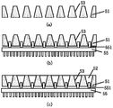
图5示出根据本发明的波长转换元件的制备方法的流程图。
图6示出根据本发明的另一结构的波长转换元件的结构示例的示意图。
图7示出根据本发明的另一结构的波长转换元件的制备方法的流程图。
图8示出根据本发明的另一结构的波长转换元件的结构示例的示意图。
图9示出根据本发明的另一结构的波长转换元件的制备方法的流程图。
图10示出根据本发明的另一结构的波长转换元件的结构示例的示意图。
图11示出根据本发明的另一结构的波长转换元件的制备方法的流程图。
图12示出图11所示的波长转换元件的支柱与凹坑侧壁调整光传播路线的示意图。
以下将结合附图对本发明各实施例的技术方案进行清楚、完整的描述,显然,所描述的实施例仅是本发明的一部分实施例,而不是全部的实施例。基于本发明中的实施例,本领域普通技术人员在没有做出创造性劳动的前提下所得到的所有其它实施例,都属于本发明所保护的范围。
注意,附图是示意性的,且不是基于实际比例绘制的。附图中图示的部件的相对尺度和比例在尺寸方面被放大或缩小,且任何尺度仅是示例性的且不具有限制性。附图中的相同的结构、元件或部件由相同的附图标记表示。
以下,将按顺序说明本发明的波长转换元件的结构及制备方法的具体示例。
<波长转换元件的结构示例>
下面,将结合图2来详细说明根据本发明的波长转换元件20的结构示例。
如图2所示,附图标记20整体地表示波长转换元件,附图标记21表示光阻隔材料,且附图标记22表示波长转换材料,且附图标记23表示凹坑。图2在上部示出波长转换元件20的平面图,且在下部示出波长转换元件20的纵向截面图。
如图2所示,波长转换元件20包括波长转换材料22和光阻隔材料21。波长转换材料22可接收从波长转换元件20的上方(图2中的纵向截 面图的上侧)入射的激发光,以产生受激光。在这里,可以选择蓝激光作为激发光,优选的蓝激光可以是波长为473nm,例如从半导体激光器获得的激光。
具体地,在光阻隔材料21中形成有二维排列的多个凹坑23,且多个波长转换材料22相应地填充在各个凹坑23中。在波长转换元件20中,凹坑23二维地排列成矩阵模式。因而,波长转换材料22被光阻隔材料21彼此间隔开,从而形成像素点阵列。然而,本发明不局限于此,且可以采用其它已知的模式。
凹坑23从光阻隔材料21的上表面朝光阻隔材料21的内部延伸,但未贯穿光阻隔材料21的整个厚度。在纵向截面图中,凹坑23形成为倒梯形,即,在纵向截面图中,凹坑23的上底尺寸大于下底尺寸。另一方面,在平面图中,凹坑23形成为正方形。在波长转换元件20中,凹坑的平面尺寸优选为0.1×0.1mm
2至1×1mm
2。由图2可见,凹坑23的尺寸确定了像素的尺寸。
应当理解,用于解释图2示出的凹坑23的纵向截面倒梯形的上下底尺寸及比例、平面形状及尺寸仅都是示例性的,且根据不同应用可以进行修改。例如,凹坑23的平面形状也可以是诸如圆形或多边形形状等其它规则形状或不规则形状。凹坑23的空间形状近似圆锥或棱锥。
另外,凹坑23的内壁表面的粗糙的。具体地,凹坑23的内壁的表面粗糙度可以为0.1μm至15μm,优选地为0.5μm至10μm。这种情况下,能够提高设置在凹坑23中的结构(例如,本实施例中的波长转换材料22)与凹坑23之间的附着力,从而提高了波长转换元件的机械性能,例如,牢固性。
优选地,波长转换材料22包括发光玻璃。玻璃粉在熔融状态下与陶瓷的润湿性能较好,从而提高了波长转换材料与光阻隔材料之间的粘附力,并进而提高了波长转换元件的机械性能及导热性能。具体地,用于形成波长转换材料22的发光玻璃包括混合的玻璃材料和荧光材料。作为光学转换材料,荧光材料可以是YAG:Ce、LuAG:Ce、LuYAG:Ce、(AE)SiON、(AE)SiAlON、(AE)AlSiN
3、(AE)
2Si
5N
8等结构之一或两种以上,其中AE为碱土金属。通过使用玻璃材料可将这些荧光材料的颗粒粘接在一起。
光阻隔材料21不透射可见光,即具有光吸收功能和/或光反射功能,以防止不同像素间的光串扰。优选地,光阻隔材料21包括无机材料,从而在高温下依然能够稳定工作。另外,考虑到与波长转换材料的相容性,光阻隔材料21优选包括无机非金属材料。光阻隔材料21可以是对可见光具有较强反射的Al
2O
3陶瓷,也可以是对可见光具有强烈吸收的硅片、AlN陶瓷等,以防止相邻发光像素之间的串扰。在波长转换元件20中,光阻隔材料21采用Al
2O
3陶瓷。
由于波长转换元件的凹坑纵截面呈倒梯形,所以优选地,可以在凹坑内壁设置有光反射层(未图示),光反射层包括但不限于金属光反射层。例如,通过镀膜工艺在凹坑内壁镀设一层银光反射层,由此有利于提高波长转换元件的出光效率。
在本发明中,通过激光刻蚀在光阻隔材料21中形成二维排列的凹坑23。由激光刻蚀的性能可知,凹坑23的纵向截面形状为倒梯形,以有利于发光玻璃浆料的填充。凹坑23的深度可通过控制刻蚀时间来实现。
波长转换材料22是采用刮涂法通过将均匀混合有玻璃粉、荧光粉和有机载体的荧光粉浆料填满凹坑并之后进行干燥、烧结过程获得的。由于荧光粉浆料在干燥过程中收缩严重,使得发光材料无法完全填满凹坑阵列,因而,可交替地重复2至3次刮涂过程和干燥过程,以减少由于干燥收缩引起的发光玻璃无法填满凹坑的问题。
图3示出了根据本发明的波长转换元件在显微镜下的照片。在图3所示的结构中,各个像素点的尺寸为0.2mm,且光阻隔材料的厚度也为0.2mm。从图3中可以看出,发光玻璃填满了凹坑阵列,且在发光玻璃和光阻隔材料之间不存在任何缝隙。
与现有技术例如欧司朗专利申请所使用的陶瓷发光材料不同,本发明的波长转换材料22使用发光玻璃。发光玻璃在烧结过程为熔融状态,该状态有利于发光玻璃填满凹坑,并且发光玻璃与采用Al
2O
3陶瓷材料的光阻隔材料21的界面接触紧密,具有较高的机械性能。因此,根据本发明,得到的波长转换元件中的发光玻璃与光阻隔材料粘结良好,大大地改善了器机械性能和导热性能。
图4示出了根据本发明的波长转换元件的摔碎状态的纵向截面照片,其中图4的(a)示出了在使用1h的激光刻蚀得到的凹坑中填充发光玻璃的情形,且图4的(b)示出了在使用30min的激光刻蚀得到的凹坑中填充发光玻璃的情形。从图4中可以看出,激光刻蚀时间越长,则凹坑深度越深。另外,发光玻璃与Al
2O
3光阻隔材料粘结良好,且摔碎之后未出现发光玻璃拔出等现象,这表明本发明的波长转换元件具有良好的机械性能和可靠性。
<波长转换元件的制备方法示例>
下面,将结合图5来详细说明制备根据本发明的波长转换元件20的方法。
图5示出根据本发明的波长转换元件20的制备方法的流程图。
首先,在第一步骤中,提供氧化铝陶瓷材料21。在第二步骤中,如图5的(a)所示,在氧化铝陶瓷材料21上,利用激光刻蚀形成二维排列的凹坑23。例如,凹坑23的平面形状可以是正方形。在波长转换元件20中,优选地,凹坑的平面尺寸为0.1×0.1mm
2至1×1mm
2。凹坑尺寸确定了像素的尺寸。
由于激光刻蚀的特性,得到的凹坑的纵向截面形状为倒梯形。可以通过调节激光功率来调节纵向截面倒梯形的上底和下底的比例。而且,可通过控制刻蚀时间来调节凹坑的深度。这种上大下小形状的凹坑有利于填充发光玻璃材料。
另外,根据激光刻蚀的特性,形成的凹坑的内壁表面是粗糙的。然而,为了在有利于后面形成在凹坑中的结构(例如,本实施例中的发光玻璃材料)牢固地结合在凹坑中的同时不使波长转换材料的性能劣化,根据本发明,适当地调节激光刻蚀的工艺参数,使得凹坑23的内壁的表面粗糙度可以为0.1μm至15μm,优选地为0.5μm至10μm。
可替代地,通过镀膜工艺进一步在凹坑的内壁上设置光反射层。光反射层包括但不限于金属光反射层。例如,金属光反射层为银光反射层。
接着,在第三步骤中,制备用于形成发光玻璃材料22的浆料。具体地,将玻璃粉、荧光粉和有机载体按照期望比例混合均匀,以得到含荧 光粉的玻璃浆料。有机载体采用乙基纤维素与松油醇、丁基卡比醇、丁基卡比醇酯混合而成。乙基纤维素起到粘接剂和成膜剂的作用,其含量占整个有机载体的3至10重量%。乙基纤维素含量越高,粘度越大,成膜性越好,但是在刮涂过程中流动性越差,越难填满整个凹坑。在此制备方法中,乙基纤维素在有机载体中的含量优选为6重量%。有机载体中的松油醇、丁基卡比醇和丁基卡比醇酯起到溶剂的作用。这些溶剂的沸点依次升高,从而按照一定的沸程梯度挥发,并防止溶剂集中挥发影响膜层表面特性和均匀性。在本制备方法中松油醇、丁基卡比醇和丁基卡比醇酯在整个有机载体中的含量分别为70重量%、12重量%、12重量%。
接着,在第四步骤中,如图5的(b)所示,采用刮涂法使荧光粉玻璃浆料填满凹坑23。然后,在第五步骤中,在例如160至200℃的温度下对获得的结构进行预烘干,并在例如600至1200℃的温度下进行烧结。由此,得到像素化波长转换元件20。注意,由于玻璃浆料在干燥过程中收缩严重,使得发光玻璃材料无法完全填满凹坑,因而,可重复2至3次刮涂和干燥过程,以减少由于干燥收缩引起的发光玻璃材料22无法填满凹坑的问题。
在本发明中,由于仅对玻璃浆料进行烧结,因此本发明的烧结温度与对陶瓷材料的烧结过程相比相对较低,从而避免了高温烧结过程。
另外,作为可能的额外步骤,在烧结得到波长转换元件之后,对其上表面进行抛光处理,以此除去在刮涂过程中可能残留在光阻隔材料的上表面上的发光玻璃材料。
此外,作为可能的额外步骤,还可以在抛光后的上表面进行图案化或镀覆各种光学膜(如增透膜,以提高像素化波长转换材料的出光效率)。
因此,如上所述,在欧司朗的专利申请的方法中,由于陶瓷烧结过程中尺寸收缩,所以这些方法无法精确调控各个像素点的尺寸。相对比地,在本发明中,通过激光刻蚀在已经烧结的阻隔材料上刻蚀凹坑阵列,激光刻蚀方法简单,不需要掩膜,且尺寸控制更精确。
另外,在本发明中,与欧司朗专利申请中所使用的陶瓷发光材料不同,发光玻璃在烧结过程为熔融状态,该状态有利于发光玻璃填满凹坑阵列,并且发光玻璃与Al
2O
3陶瓷的界面接触紧密,具有较高的机械性能。 根据本发明得到的波长转换元件中的发光玻璃与光阻隔材料粘结良好,大大地改善了器机械性能、导热性能和可靠性能。
<波长转换元件的另一结构示例>
在一些实施方式中,波长转换元件还可以具有其它的结构。
如图6所示,附图标记30整体地表示波长转换元件,附图标记31表示光阻隔材料,附图标记32表示波长转换材料,附图标记33表示凹坑,且附图标记34表示底层。图6在上部示出波长转换元件30的平面图,且在下部示出波长转换元件30的纵向截面图。
与图2所示的结构相比,在图6所示的结构中,在二维地排列在光阻隔材料31中的各凹坑33中,除了波长转换材料32之外,在波长转换材料32的下部还设置有底层34。也就是说,在凹坑33中设置有包括波长转换材料32和底层34的双层结构。除此之外,图6所示的结构与图2所示的结构完全相同,且在下面省略了对相同部分的说明。
底层34是具有较高的反射率和导热系数的玻璃材料,且优选为纳米银粉和玻璃粉烧结成的烧结银。
根据波长转换元件30,由于烧结银具有较高的导热率和反射率,因而相比于波长转换元件20,可进一步提高该波长转换元件的性能。
<波长转换元件的另一制备方法示例>
下面,将结合图7来详细说明制备波长转换元件30的方法。
图7示出波长转换元件30的制备方法的流程图。
首先,如同图5所示的制备方法,在第一步骤中,如图7的(a)所示,提供氧化铝陶瓷材料31,。接着,在第二步骤中,如图7的(a)所示,并利用激光刻蚀在氧化铝陶瓷材料31上形成二维排列的凹坑33。具体过程在此不再赘述。类似地,在图7的(a)的步骤中,可选择地,通过镀膜工艺进一步在凹坑的内壁上设置光反射层。光反射层包括但不限于金属光反射层。例如,金属光反射层为银光反射层。
接着,与图5所示的制备方法不同的是,在第三步骤中,在将用于形 成发光玻璃材料22的浆料填满凹坑33之前,将纳米银粉、玻璃粉、有机载体按照期望比例混合均匀,从而得到用于形成底层34的浆料。然后,如图7的(b)所示,在第四步骤中,通过诸如精密点胶机等仪器控制步长将浆料滴入光阻隔材料的凹坑32中。然后,在第五步骤中,通过干燥及烧结处理,在凹坑下底部形成有烧结的底层34。
接着,如同图5所示的制备方法,在第六步骤中,将玻璃粉、荧光粉和有机载体按照期望比例混合均匀,以得到含荧光粉的玻璃浆料,并在第七步骤中,如图7的(c)所示,采用刮涂法使荧光粉玻璃浆料填满凹坑33。然后,在第八步骤中,在例如160至200℃的温度下对获得的结构进行预烘干,并在第九步骤中,在例如600至1200℃的温度下进行烧结。由此,得到像素化波长转换元件30。具体过程在此不再赘述。
根据由图7所示的制备方法产生的波长转换元件30,由于烧结银具有较高的导热率和反射率,因而相对于波长转换元件20可进一步提高波长转换元件的性能。
<波长转换元件的另一结构示例>
在一些实施方式中,波长转换元件还可以具有其它的结构。
如图8所示,附图标记40整体地表示波长转换元件,附图标记41表示光阻隔材料,附图标记42表示波长转换材料,附图标记43表示凹坑,附图标记44表示底层,且附图标记45表示散热器。图8在上部示出波长转换元件40的平面图,且在下部示出波长转换元件40的纵向截面图。
图8所示的结构是对图6所示的结构的改进。具体地,在波长转换元件40中,底层44从光阻隔材料41的底层侧的表面处露出,且散热器45焊接至各底层44。例如,如图8所示,散热器45经由一侧的支柱451焊接至各底层44。为此,支柱451在散热器45上的排列方式必定与形成有底层44的凹坑43的排列方式相同。也就是说,支柱451形成在散热器45的与各凹坑43相对应的位置处。这里,支柱451可以是金属材料,也可以是陶瓷材料,还可以是其他具有良好导热的材料,这样可以将从底层44传导来热量迅速传递到散热器45上。
在图8所示的结构中,波长转换材料42产生的热量能够经由底层44传递到散热器45,由此提高了波长转换元件40的散热能力。
根据图8所示的结构,进一步提高了波长转换元件的散热能力,并从而提高了波长转换元件的热学性能。
<波长转换元件的另一制备方法示例>
下面,将结合图9来详细说明制备波长转换元件40的方法。
图9示出波长转换元件40的制备方法的流程图。
注意,图9的(a)至(c)所涉及的第一步骤至第九步骤与图7的(a)至(c)所示的第一步骤至第九步骤完全相同,在此不再赘述。类似地,在图9的(a)的步骤中,可选择地,通过镀膜工艺进一步在凹坑的内壁上设置光反射层。光反射层包括但不限于金属光反射层。例如,金属光反射层为银光反射层。
接着,在第十步骤中,如图9的(d)所示,对光阻隔材料41的底层侧的表面(即,下表面)进行减薄和抛光处理,直至露出底层44。
然后,在第十一步骤中,如图9的(e)所示,通过诸如精密点胶机等设备,在底层44的露出表面上滴加适量的焊料,并将焊接散热器焊接至底层44,由此得到波长转换元件40。
<波长转换元件的另一结构示例>
在一些实施方式中,波长转换元件还可以具有其它的结构。
如图10所示,附图标记50整体地表示波长转换元件,附图标记51表示光阻隔材料,附图标记52表示波长转换材料,附图标记53表示凹坑,且附图标记55表示散热器。图10在上部示出波长转换元件50的平面图,且在下部示出波长转换元件50的纵向截面图。
与图8所示的结构相比,在图10所示的结构中,在凹坑53中不再形成有底层,且散热器55的支柱551的至少一部分插入到凹坑中并嵌入在波长转换材料52中。这里,支柱551可以是金属材料,也可以是陶瓷材料,还可以是其他具有良好导热和/或反光效果的材料。
根据波长转换元件50,由于波长转换材料52分别与凹坑53的内壁和支柱551粘接,所以相对于图8所示的结构,波长转换元件50的可靠性可以进一步提高。
另外,支柱551的尺寸可以对应于凹坑53的具有较小尺寸的下底的尺寸。由此,相对于图8所示的结构,波长转换元件50的牢固性可以进一步提高。
再者,散热器55的支柱551的至少一部分插入到凹坑53中,使得支柱551的至少一部分嵌入在波长转换材料52中并与之直接接触,从而提高了热传导面积。因此,相对于图8所示的结构,波长转换元件50的散热能力可以进一步提高。
另外,优选地,可以将嵌入在波长转换材料52中的支柱的至少一部分进行粗化处理,而其它部分进行抛光处理。粗化处理部分可以提升支柱551与波长转换材料52的附着效果,且抛光处理部分具有较高的反射作用。
如图12所示,当采用上述结构时,支柱551的反射功能可配合凹坑53的侧壁的反射功能对荧光材料受激发出的光的传播路线进行调整,使得大部分光最终以近似垂直凹坑上底边的小角度出射。并且,由于波长转换元件50的尺寸较小,且各个荧光像素点通常为毫米级或微米级,所以出射光在波长转换元件500内的光程较短,使得出射光从凹坑53的上底边出射时较为集中。通过实验研究发现当凹坑的锥面或锥面母线与上底面夹角为45°时,与支柱配合,波长转换元件的出光效率最高。
<波长转换元件的另一制备方法示例>
下面,将结合图11来详细说明制备波长转换元件50的方法。
首先,类似于前述的制备方法,在第一步骤中,提供氧化铝陶瓷材料51,并在第二步骤中,如图11的(a)所示,利用激光刻蚀在氧化铝陶瓷材料51上形成二维排列的凹坑53。但与前述的制备方法不同的是,凹坑53形成为贯穿整个氧化铝陶瓷材料51。可选择地,通过镀膜工艺进一步在凹坑的内壁上设置光反射层。光反射层包括但不限于金属光反射层。例如,金属光反射层为银光反射层。
接着,在第三步骤中,提供散热器55。如上所述,散热器55在其一侧形成有支柱551。支柱551在散热器55上的排列方式与形成有底层44的凹坑43的排列方式完全相同。也就是说,支柱551形成在散热器55的与各凹坑53相对应的位置处。另外,支柱551的尺寸可以对应于凹坑53的具有较小尺寸的下底的尺寸。这里,支柱551可以是金属材料,也可以是陶瓷材料,还可以是其他具有良好导热和/或反光效果的材料。
优选地,对将要嵌入在波长转换材料52中的支柱的至少一部分进行粗化处理,而对其它部分进行抛光处理,以提高波长转换元件的出光效率。
在第四步骤中,如图11的(b)所示,将散热器55的各个支柱551从氧化铝陶瓷材料51的下表面插入到相应的凹坑53中,使得支柱551的至少一部分位于凹坑53中。
然后,在第五步骤中,制备用于形成发光玻璃材料52的浆料。发光玻璃材料52的浆料的制备方式和工艺和前述制备方法相同,在此不再赘述。
接着,在第六步骤中,类似于前述的制备方法,如图11的(c)所示,采用刮涂法使荧光粉玻璃浆料填满凹坑53,以掩埋支柱551。然后,在第七步骤中,在例如160至200℃的温度下对获得的结构进行预烘干,并在第八步骤中,在例如600至1200℃的温度下进行烧结。注意,由于玻璃浆料在干燥过程中收缩严重,使得发光玻璃材料无法完全填满凹坑,因而,可重复2至3次刮涂和干燥过程,以减少由于干燥收缩引起的发光玻璃材料52无法填满凹坑的问题。
由此,得到像素化波长转换元件50。
根据由本制备方法产生的波长转换元件50,由于波长转换材料52分别与凹坑53的内壁和支柱551粘接,且支柱551的尺寸对应于凹坑53的具有较小尺寸的下底的尺寸。由此,相对于波长转换元件40,波长转换元件50的可靠性和牢固性可以进一步提高。再者,波长转换材料52直接与支柱551接触,且接触面积较大,因此相对于波长转换元件40,波长转换元件50的散热能力可以进一步提高。
尽管通过不同的结构或不同的制备方法详细说明了本发明的波长转换元件,但根据需要可以在这些不同结构或不同制备方法之间进行各个要素的组合或替换,以产生新的结构或制备方法,且这些新的结构或制备方法并没有脱离本发明的精神和保护范围。
尽管在上面已经参照附图说明了根据本发明的波长转换元件及其制备方法,但是本发明不限于此,且本领域技术人员应理解,在不偏离本发明随附权利要求书限定的实质或范围的情况下,可以做出各种改变、组合、次组合以及变型。
Claims (24)
- 一种波长转换元件,包括:光阻隔材料,在所述光阻隔材料中形成有二维排列的多个凹坑,所述凹坑在纵向截面中为倒梯形,所述凹坑的内壁的表面粗糙度为0.1μm至15μm;以及波长转换材料,所述波长转换材料设置在所述光阻隔材料的各个所述凹坑中,且所述波长转换材料的上表面与所述光阻隔材料的上表面齐平,以用于从所述光阻隔材料的上表面接收外部的激发光以产生受激光,所述波长转换元件还包括具有导热和光反射功能的底层,所述底层设置在所述光阻隔材料的各个所述凹坑的底部。
- 根据权利要求1所述的波长转换元件,其中,所述凹坑贯穿所述光阻隔材料的整个厚度,使得各个所述底层从所述光阻隔材料的下表面露出,并且所述波长转换元件还包括散热器,所述散热器形成有与所述凹坑具有相同排列方式的多个支柱,且经由所述支柱连接到从所述光阻隔材料的下表面露出的各个所述底层。
- 一种波长转换元件,包括:光阻隔材料,在所述光阻隔材料中形成有二维排列的多个凹坑,所述凹坑在纵向截面中为倒梯形,所述凹坑的内壁的表面粗糙度为0.1μm至15μm;以及波长转换材料,所述波长转换材料设置在所述光阻隔材料的各个所述凹坑中,且所述波长转换材料的上表面与所述光阻隔材料的上表面齐平,以用于从所述光阻隔材料的上表面接收外部的激发光以产生受激光,所述凹坑贯穿所述光阻隔材料的整个厚度,使得所述波长转换材料从所述光阻隔材料的下表面露出,并且所述波长转换元件还包括散热器,所述散热器形成有与所述凹坑具有相同排列方式的多个支柱,且所述支柱的至少一部分从所述光阻隔材料的下表面插入到所述凹坑中,使得所述支柱嵌入在所述波长转换材料 中。
- 根据权利要求1至3中任一项所述的波长转换元件,其中,所述波长转换材料包括玻璃材料和荧光材料。
- 根据权利要求1至3中任一项所述的波长转换元件,其中,所述光阻隔材料为无机非金属材料。
- 根据权利要求5所述的波长转换元件,其中,所述无机非金属材料为Al 2O 3陶瓷、硅片或AlN陶瓷。
- 根据权利要求1或2所述的波长转换元件,其中,所述底层包括由纳米银粉和玻璃粉烧结成的烧结银。
- 根据权利要求3所述的波长转换元件,其中,所述支柱的尺寸对应于所述倒梯形的下底尺寸。
- 根据权利要求3所述的波长转换元件,其中,位于所述凹坑中的所述支柱的至少一部分受到表面粗化处理。
- 根据权利要求1至3中任一项所述的波长转换元件,其中,所述凹坑的内壁的表面粗糙度为0.5μm至10μm。
- 根据权利要求1至3中任一项所述的波长转换元件,其中,所述凹坑的内壁上设置有光反射层。
- 一种用于制备波长转换元件的方法,包括:提供光阻隔材料;通过激光刻蚀在所述光阻隔材料中形成二维排列的多个凹坑,其中,所述凹坑在纵向截面中形成为倒梯形,所述凹坑的内壁的表面粗糙度为0.1μm至15μm;通过混合纳米银粉、玻璃粉和有机载体来制备底层浆料;进行刮涂处理以将所述底层浆料填充在各个所述凹坑中;对所述底层浆料进行干燥处理和烧结处理,以形成底层;通过混合玻璃粉、荧光粉和有机载体来制备波长转换材料浆料;进行刮涂处理以将所述波长转换材料浆料填充在各个所述凹坑中的所述底层上方;对所述波长转换材料浆料进行干燥处理;并且对所述波长转换材料浆料进行烧结处理,以形成波长转换材料,其中,所述波长转换材料的上表面与所述光阻隔材料的上表面齐平,其中,针对所述波长转换材料浆料的刮涂处理和干燥处理交替地重复两次以上。
- 根据权利要求12所述的方法,其中,所述方法在形成所述波长转换材料之后的步骤之后还包括:对所述光阻隔材料的下表面进行减薄和抛光处理,使得所述底层从所述光阻隔材料的下表面露出;并且将散热器连接至从所述光阻隔材料的下表面露出的各个所述底层。
- 一种用于制备波长转换元件的方法,包括:提供光阻隔材料;通过激光刻蚀在所述光阻隔材料中形成二维排列的多个凹坑,其中,所述凹坑贯穿所述光阻隔材料的整个厚度,所述凹坑在纵向截面中形成为倒梯形,所述凹坑的内壁的表面粗糙度为0.1μm至15μm;提供散热器,其中,所述散热器形成有多个支柱,且所述支柱的排列方式与所述凹坑的排列方式相同;将所述散热器的各个所述支柱穿过所述下底插入到相应的所述凹坑中,使得所述支柱的至少一部分位于所述凹坑中;通过混合玻璃粉、荧光粉和有机载体来制备波长转换材料浆料;进行刮涂处理以将所述波长转换材料浆料填充在各个所述凹坑中以掩埋所述支柱;对所述波长转换材料浆料进行干燥处理;并且对所述波长转换材料浆料进行烧结处理,以形成波长转换材料,其中,所述波长转换材料的上表面与所述光阻隔材料的上表面齐平,其中,针对所述波长转换材料浆料的刮涂处理和干燥处理交替地重复两次以上。
- 根据权利要求12至14中任一项所述的方法,其中,所述光阻隔材料为无机非金属材料。
- 根据权利要求15所述的方法,其中,所述无机非金属材料为Al 2O 3陶瓷、硅片或AlN陶瓷。
- 根据权利要求12至14中任一项所述的方法,其中,所述有机载体由乙基纤维素、松油醇、丁基卡比醇和丁基卡比醇酯混合而成。
- 根据权利要求17所述的方法,其中,乙基纤维素在所述有机载体中的含量为3至10重量%。
- 根据权利要求18所述的方法,其中,乙基纤维素、松油醇、丁基卡比醇和丁基卡比醇在所述有机载体中的含量分别为6重量%、70重量%、12重量%和12重量%。
- 根据权利要求12至14中任一项所述的方法,其中,所述方法在对所述波长转换材料浆料进行所述烧结处理的步骤之后还包括:对所述光阻隔材料的露出所述波长转换材料的上表面进行图案化和/或光学膜镀覆。
- 根据权利要求14所述的方法,其中,所述支柱的尺寸对应于所述倒梯形的下底尺寸。
- 根据权利要求14所述的方法,其中,位于所述凹坑中的所述支柱的至少一部分受到表面粗化处理。
- 根据权利要求12至14中任一项所述的方法,其中,所述凹坑的内壁的表面粗糙度为0.5μm至10μm。
- 根据权利要求12至14中任一项所述的方法,其中,所述方法在形成所述凹坑的步骤之后还包括:通过镀膜工艺在所述凹坑的内壁上设置光反射层。
Applications Claiming Priority (2)
| Application Number | Priority Date | Filing Date | Title |
|---|---|---|---|
| CN201711061898.3A CN109755355B (zh) | 2017-11-02 | 2017-11-02 | 波长转换元件及其制备方法 |
| CN201711061898.3 | 2017-11-02 |
Publications (1)
| Publication Number | Publication Date |
|---|---|
| WO2019085259A1 true WO2019085259A1 (zh) | 2019-05-09 |
Family
ID=66332774
Family Applications (1)
| Application Number | Title | Priority Date | Filing Date |
|---|---|---|---|
| PCT/CN2018/071433 Ceased WO2019085259A1 (zh) | 2017-11-02 | 2018-01-04 | 波长转换元件及其制备方法 |
Country Status (2)
| Country | Link |
|---|---|
| CN (1) | CN109755355B (zh) |
| WO (1) | WO2019085259A1 (zh) |
Cited By (3)
| Publication number | Priority date | Publication date | Assignee | Title |
|---|---|---|---|---|
| CN111425820A (zh) * | 2020-04-24 | 2020-07-17 | 超视界激光科技(苏州)有限公司 | 一种波长转换单元及激光照明模组 |
| CN113024253A (zh) * | 2019-12-09 | 2021-06-25 | 上海航空电器有限公司 | 用于激光照明的高显色性包边复合结构波长转换陶瓷及其制备方法 |
| CN114664998A (zh) * | 2020-12-22 | 2022-06-24 | 北京航空航天大学合肥创新研究院 | 色转换基板及其制作方法、颜色转换显示器件 |
Families Citing this family (2)
| Publication number | Priority date | Publication date | Assignee | Title |
|---|---|---|---|---|
| CN112216774A (zh) * | 2019-07-11 | 2021-01-12 | 成都辰显光电有限公司 | 色彩转换组件、显示面板及制作方法 |
| CN112750862B (zh) * | 2019-10-31 | 2022-11-11 | 成都辰显光电有限公司 | 色彩转换结构、显示装置及色彩转换结构的制备方法 |
Citations (6)
| Publication number | Priority date | Publication date | Assignee | Title |
|---|---|---|---|---|
| CN105684171A (zh) * | 2013-10-29 | 2016-06-15 | 欧司朗光电半导体有限公司 | 波长转换元件、制造方法和具有波长转换元件的发光半导体部件 |
| CN105762239A (zh) * | 2016-04-12 | 2016-07-13 | 杨阳 | 光转换装置及其制备方法和应用 |
| CN106030836A (zh) * | 2014-03-10 | 2016-10-12 | 欧司朗光电半导体有限公司 | 波长转换元件、包括波长转换元件的发光半导体部件、用于制造波长转换元件的方法和用于制造包括波长转换元件的发光半导体部件的方法 |
| CN106449947A (zh) * | 2015-08-11 | 2017-02-22 | 台达电子工业股份有限公司 | 波长转换装置 |
| US20170110636A1 (en) * | 2012-03-14 | 2017-04-20 | Samsung Electronics Co., Ltd. | Light emitting element package and method of manufacturing the same |
| CN107272317A (zh) * | 2017-05-31 | 2017-10-20 | 深圳市光峰光电技术有限公司 | 荧光芯片及其波长转换装置的制备方法以及显示系统 |
Family Cites Families (5)
| Publication number | Priority date | Publication date | Assignee | Title |
|---|---|---|---|---|
| CN103222073B (zh) * | 2010-08-03 | 2017-03-29 | 财团法人工业技术研究院 | 发光二极管芯片、发光二极管封装结构、及用以形成上述的方法 |
| CN104205375B (zh) * | 2012-03-30 | 2019-01-15 | 亮锐控股有限公司 | 包括发光器件和波长转换材料的光学腔 |
| CN103792768B (zh) * | 2012-10-31 | 2015-09-09 | 深圳市绎立锐光科技开发有限公司 | 光源系统及相关投影系统 |
| CN104091860B (zh) * | 2014-07-01 | 2017-01-11 | 东莞市万丰纳米材料有限公司 | Led封装光源及其生产工艺 |
| CN106896632A (zh) * | 2015-12-03 | 2017-06-27 | 精工爱普生株式会社 | 荧光体、波长转换元件、光源装置和投影仪 |
-
2017
- 2017-11-02 CN CN201711061898.3A patent/CN109755355B/zh active Active
-
2018
- 2018-01-04 WO PCT/CN2018/071433 patent/WO2019085259A1/zh not_active Ceased
Patent Citations (6)
| Publication number | Priority date | Publication date | Assignee | Title |
|---|---|---|---|---|
| US20170110636A1 (en) * | 2012-03-14 | 2017-04-20 | Samsung Electronics Co., Ltd. | Light emitting element package and method of manufacturing the same |
| CN105684171A (zh) * | 2013-10-29 | 2016-06-15 | 欧司朗光电半导体有限公司 | 波长转换元件、制造方法和具有波长转换元件的发光半导体部件 |
| CN106030836A (zh) * | 2014-03-10 | 2016-10-12 | 欧司朗光电半导体有限公司 | 波长转换元件、包括波长转换元件的发光半导体部件、用于制造波长转换元件的方法和用于制造包括波长转换元件的发光半导体部件的方法 |
| CN106449947A (zh) * | 2015-08-11 | 2017-02-22 | 台达电子工业股份有限公司 | 波长转换装置 |
| CN105762239A (zh) * | 2016-04-12 | 2016-07-13 | 杨阳 | 光转换装置及其制备方法和应用 |
| CN107272317A (zh) * | 2017-05-31 | 2017-10-20 | 深圳市光峰光电技术有限公司 | 荧光芯片及其波长转换装置的制备方法以及显示系统 |
Cited By (4)
| Publication number | Priority date | Publication date | Assignee | Title |
|---|---|---|---|---|
| CN113024253A (zh) * | 2019-12-09 | 2021-06-25 | 上海航空电器有限公司 | 用于激光照明的高显色性包边复合结构波长转换陶瓷及其制备方法 |
| CN113024253B (zh) * | 2019-12-09 | 2023-09-12 | 上海航空电器有限公司 | 用于激光照明的高显色性包边复合结构波长转换陶瓷及其制备方法 |
| CN111425820A (zh) * | 2020-04-24 | 2020-07-17 | 超视界激光科技(苏州)有限公司 | 一种波长转换单元及激光照明模组 |
| CN114664998A (zh) * | 2020-12-22 | 2022-06-24 | 北京航空航天大学合肥创新研究院 | 色转换基板及其制作方法、颜色转换显示器件 |
Also Published As
| Publication number | Publication date |
|---|---|
| CN109755355A (zh) | 2019-05-14 |
| CN109755355B (zh) | 2021-12-07 |
Similar Documents
| Publication | Publication Date | Title |
|---|---|---|
| CN109755355B (zh) | 波长转换元件及其制备方法 | |
| US8552444B2 (en) | Semiconductor light-emitting device and manufacturing method of the same | |
| US9590146B2 (en) | Method for fabrication of a luminescent structure | |
| US9337398B2 (en) | Phosphor in inorganic binder for LED applications | |
| CN101569024B (zh) | 半导体发光器件及半导体发光装置的制造方法 | |
| JP5322801B2 (ja) | 半導体発光装置及びその製造方法 | |
| WO2016092956A1 (ja) | 発光装置用基板及び発光装置用基板の製造方法 | |
| TW201242108A (en) | Producing method of light emitting element transfer sheet, producing method of light emitting device, light emitting element transfer sheet, and light emitting device | |
| KR20070054725A (ko) | 현탁액으로부터 용매 증발을 통해 반도체 발광 소자를코팅하는 방법 | |
| CN103890983B (zh) | 光电子器件和用于制造光电子器件的方法 | |
| JP2011529267A (ja) | 窓層及び光指向構造を含む半導体発光装置 | |
| US11824148B2 (en) | Semiconductor light emitting devices and method of manufacturing the same | |
| JP2012517697A (ja) | 光素子用基板、これを有する光素子パッケージおよびその製造方法 | |
| JP2017054894A (ja) | 発光装置 | |
| TW201133954A (en) | Fabrication method of light emitting diode chip having phosphor coating layer | |
| CN105914275A (zh) | 倒装发光二极管及其制作方法 | |
| CN109681846A (zh) | 波长转换装置及其制备方法 | |
| CN106605013A (zh) | 用于制造横向结构化的磷光层的方法和具有这种磷光层的光电子半导体组件 | |
| JP5748575B2 (ja) | 発光装置 | |
| JP7174290B2 (ja) | 発光装置及び発光装置の製造方法 | |
| JP6521119B2 (ja) | 発光装置 | |
| JP6974702B2 (ja) | 半導体発光装置の製造方法 | |
| WO2019024365A1 (zh) | 荧光芯片及其制造方法和发光装置 | |
| CN113644169B (zh) | 一种红光led芯片及其制造方法 | |
| WO2013108738A1 (ja) | 発光装置 |
Legal Events
| Date | Code | Title | Description |
|---|---|---|---|
| 121 | Ep: the epo has been informed by wipo that ep was designated in this application |
Ref document number: 18872835 Country of ref document: EP Kind code of ref document: A1 |
|
| NENP | Non-entry into the national phase |
Ref country code: DE |
|
| 122 | Ep: pct application non-entry in european phase |
Ref document number: 18872835 Country of ref document: EP Kind code of ref document: A1 |