WO2019082847A1 - 表示装置及び表示装置の製造方法 - Google Patents
表示装置及び表示装置の製造方法Info
- Publication number
- WO2019082847A1 WO2019082847A1 PCT/JP2018/039202 JP2018039202W WO2019082847A1 WO 2019082847 A1 WO2019082847 A1 WO 2019082847A1 JP 2018039202 W JP2018039202 W JP 2018039202W WO 2019082847 A1 WO2019082847 A1 WO 2019082847A1
- Authority
- WO
- WIPO (PCT)
- Prior art keywords
- layer
- inorganic insulating
- resin layer
- insulating layer
- display device
- Prior art date
- Legal status (The legal status is an assumption and is not a legal conclusion. Google has not performed a legal analysis and makes no representation as to the accuracy of the status listed.)
- Ceased
Links
Images




Classifications
-
- H—ELECTRICITY
- H10—SEMICONDUCTOR DEVICES; ELECTRIC SOLID-STATE DEVICES NOT OTHERWISE PROVIDED FOR
- H10K—ORGANIC ELECTRIC SOLID-STATE DEVICES
- H10K77/00—Constructional details of devices covered by this subclass and not covered by groups H10K10/80, H10K30/80, H10K50/80 or H10K59/80
- H10K77/10—Substrates, e.g. flexible substrates
- H10K77/111—Flexible substrates
-
- G—PHYSICS
- G09—EDUCATION; CRYPTOGRAPHY; DISPLAY; ADVERTISING; SEALS
- G09F—DISPLAYING; ADVERTISING; SIGNS; LABELS OR NAME-PLATES; SEALS
- G09F9/00—Indicating arrangements for variable information in which the information is built-up on a support by selection or combination of individual elements
- G09F9/30—Indicating arrangements for variable information in which the information is built-up on a support by selection or combination of individual elements in which the desired character or characters are formed by combining individual elements
-
- H—ELECTRICITY
- H05—ELECTRIC TECHNIQUES NOT OTHERWISE PROVIDED FOR
- H05B—ELECTRIC HEATING; ELECTRIC LIGHT SOURCES NOT OTHERWISE PROVIDED FOR; CIRCUIT ARRANGEMENTS FOR ELECTRIC LIGHT SOURCES, IN GENERAL
- H05B33/00—Electroluminescent light sources
- H05B33/02—Details
- H05B33/06—Electrode terminals
-
- H—ELECTRICITY
- H05—ELECTRIC TECHNIQUES NOT OTHERWISE PROVIDED FOR
- H05B—ELECTRIC HEATING; ELECTRIC LIGHT SOURCES NOT OTHERWISE PROVIDED FOR; CIRCUIT ARRANGEMENTS FOR ELECTRIC LIGHT SOURCES, IN GENERAL
- H05B33/00—Electroluminescent light sources
- H05B33/10—Apparatus or processes specially adapted to the manufacture of electroluminescent light sources
-
- H—ELECTRICITY
- H05—ELECTRIC TECHNIQUES NOT OTHERWISE PROVIDED FOR
- H05B—ELECTRIC HEATING; ELECTRIC LIGHT SOURCES NOT OTHERWISE PROVIDED FOR; CIRCUIT ARRANGEMENTS FOR ELECTRIC LIGHT SOURCES, IN GENERAL
- H05B33/00—Electroluminescent light sources
- H05B33/12—Light sources with substantially two-dimensional [2D] radiating surfaces
-
- H—ELECTRICITY
- H05—ELECTRIC TECHNIQUES NOT OTHERWISE PROVIDED FOR
- H05B—ELECTRIC HEATING; ELECTRIC LIGHT SOURCES NOT OTHERWISE PROVIDED FOR; CIRCUIT ARRANGEMENTS FOR ELECTRIC LIGHT SOURCES, IN GENERAL
- H05B33/00—Electroluminescent light sources
- H05B33/12—Light sources with substantially two-dimensional [2D] radiating surfaces
- H05B33/22—Light sources with substantially two-dimensional [2D] radiating surfaces characterised by the chemical or physical composition or the arrangement of auxiliary dielectric or reflective layers
-
- H—ELECTRICITY
- H10—SEMICONDUCTOR DEVICES; ELECTRIC SOLID-STATE DEVICES NOT OTHERWISE PROVIDED FOR
- H10K—ORGANIC ELECTRIC SOLID-STATE DEVICES
- H10K50/00—Organic light-emitting devices
- H10K50/80—Constructional details
- H10K50/84—Passivation; Containers; Encapsulations
- H10K50/844—Encapsulations
-
- H—ELECTRICITY
- H10—SEMICONDUCTOR DEVICES; ELECTRIC SOLID-STATE DEVICES NOT OTHERWISE PROVIDED FOR
- H10K—ORGANIC ELECTRIC SOLID-STATE DEVICES
- H10K59/00—Integrated devices, or assemblies of multiple devices, comprising at least one organic light-emitting element covered by group H10K50/00
- H10K59/10—OLED displays
- H10K59/12—Active-matrix OLED [AMOLED] displays
- H10K59/122—Pixel-defining structures or layers, e.g. banks
-
- H—ELECTRICITY
- H10—SEMICONDUCTOR DEVICES; ELECTRIC SOLID-STATE DEVICES NOT OTHERWISE PROVIDED FOR
- H10K—ORGANIC ELECTRIC SOLID-STATE DEVICES
- H10K59/00—Integrated devices, or assemblies of multiple devices, comprising at least one organic light-emitting element covered by group H10K50/00
- H10K59/10—OLED displays
- H10K59/12—Active-matrix OLED [AMOLED] displays
- H10K59/126—Shielding, e.g. light-blocking means over the TFTs
-
- H—ELECTRICITY
- H10—SEMICONDUCTOR DEVICES; ELECTRIC SOLID-STATE DEVICES NOT OTHERWISE PROVIDED FOR
- H10K—ORGANIC ELECTRIC SOLID-STATE DEVICES
- H10K71/00—Manufacture or treatment specially adapted for the organic devices covered by this subclass
-
- H—ELECTRICITY
- H10—SEMICONDUCTOR DEVICES; ELECTRIC SOLID-STATE DEVICES NOT OTHERWISE PROVIDED FOR
- H10K—ORGANIC ELECTRIC SOLID-STATE DEVICES
- H10K71/00—Manufacture or treatment specially adapted for the organic devices covered by this subclass
- H10K71/40—Thermal treatment, e.g. annealing in the presence of a solvent vapour
-
- H—ELECTRICITY
- H10—SEMICONDUCTOR DEVICES; ELECTRIC SOLID-STATE DEVICES NOT OTHERWISE PROVIDED FOR
- H10K—ORGANIC ELECTRIC SOLID-STATE DEVICES
- H10K2102/00—Constructional details relating to the organic devices covered by this subclass
- H10K2102/301—Details of OLEDs
- H10K2102/311—Flexible OLED
-
- H—ELECTRICITY
- H10—SEMICONDUCTOR DEVICES; ELECTRIC SOLID-STATE DEVICES NOT OTHERWISE PROVIDED FOR
- H10K—ORGANIC ELECTRIC SOLID-STATE DEVICES
- H10K2102/00—Constructional details relating to the organic devices covered by this subclass
- H10K2102/301—Details of OLEDs
- H10K2102/351—Thickness
-
- H—ELECTRICITY
- H10—SEMICONDUCTOR DEVICES; ELECTRIC SOLID-STATE DEVICES NOT OTHERWISE PROVIDED FOR
- H10K—ORGANIC ELECTRIC SOLID-STATE DEVICES
- H10K59/00—Integrated devices, or assemblies of multiple devices, comprising at least one organic light-emitting element covered by group H10K50/00
- H10K59/10—OLED displays
- H10K59/12—Active-matrix OLED [AMOLED] displays
- H10K59/1201—Manufacture or treatment
-
- H—ELECTRICITY
- H10—SEMICONDUCTOR DEVICES; ELECTRIC SOLID-STATE DEVICES NOT OTHERWISE PROVIDED FOR
- H10K—ORGANIC ELECTRIC SOLID-STATE DEVICES
- H10K59/00—Integrated devices, or assemblies of multiple devices, comprising at least one organic light-emitting element covered by group H10K50/00
- H10K59/10—OLED displays
- H10K59/12—Active-matrix OLED [AMOLED] displays
- H10K59/131—Interconnections, e.g. wiring lines or terminals
-
- H—ELECTRICITY
- H10—SEMICONDUCTOR DEVICES; ELECTRIC SOLID-STATE DEVICES NOT OTHERWISE PROVIDED FOR
- H10K—ORGANIC ELECTRIC SOLID-STATE DEVICES
- H10K59/00—Integrated devices, or assemblies of multiple devices, comprising at least one organic light-emitting element covered by group H10K50/00
- H10K59/80—Constructional details
- H10K59/87—Passivation; Containers; Encapsulations
- H10K59/873—Encapsulations
-
- H—ELECTRICITY
- H10—SEMICONDUCTOR DEVICES; ELECTRIC SOLID-STATE DEVICES NOT OTHERWISE PROVIDED FOR
- H10K—ORGANIC ELECTRIC SOLID-STATE DEVICES
- H10K71/00—Manufacture or treatment specially adapted for the organic devices covered by this subclass
- H10K71/80—Manufacture or treatment specially adapted for the organic devices covered by this subclass using temporary substrates
-
- Y—GENERAL TAGGING OF NEW TECHNOLOGICAL DEVELOPMENTS; GENERAL TAGGING OF CROSS-SECTIONAL TECHNOLOGIES SPANNING OVER SEVERAL SECTIONS OF THE IPC; TECHNICAL SUBJECTS COVERED BY FORMER USPC CROSS-REFERENCE ART COLLECTIONS [XRACs] AND DIGESTS
- Y02—TECHNOLOGIES OR APPLICATIONS FOR MITIGATION OR ADAPTATION AGAINST CLIMATE CHANGE
- Y02E—REDUCTION OF GREENHOUSE GAS [GHG] EMISSIONS, RELATED TO ENERGY GENERATION, TRANSMISSION OR DISTRIBUTION
- Y02E10/00—Energy generation through renewable energy sources
- Y02E10/50—Photovoltaic [PV] energy
- Y02E10/549—Organic PV cells
-
- Y—GENERAL TAGGING OF NEW TECHNOLOGICAL DEVELOPMENTS; GENERAL TAGGING OF CROSS-SECTIONAL TECHNOLOGIES SPANNING OVER SEVERAL SECTIONS OF THE IPC; TECHNICAL SUBJECTS COVERED BY FORMER USPC CROSS-REFERENCE ART COLLECTIONS [XRACs] AND DIGESTS
- Y02—TECHNOLOGIES OR APPLICATIONS FOR MITIGATION OR ADAPTATION AGAINST CLIMATE CHANGE
- Y02P—CLIMATE CHANGE MITIGATION TECHNOLOGIES IN THE PRODUCTION OR PROCESSING OF GOODS
- Y02P70/00—Climate change mitigation technologies in the production process for final industrial or consumer products
- Y02P70/50—Manufacturing or production processes characterised by the final manufactured product
Definitions
- the present invention relates to a display device and a method of manufacturing the display device.
- One embodiment of the present invention relates to a flexible display device formed using a flexible substrate, and a method of manufacturing the flexible display device.
- Examples of the display device include a liquid crystal display device and an organic electroluminescence (EL) display device. These display devices each have a liquid crystal element or an organic light emitting element (hereinafter, light emitting element) as a display element in each of a plurality of pixels formed on a substrate.
- a liquid crystal element or a light emitting element a layer containing a compound exhibiting liquid crystallinity (hereinafter referred to as a liquid crystal layer) or a layer containing an organic compound exhibiting electroluminescence (hereinafter referred to as an electroluminescent layer or an EL layer) is interposed between a pair of electrodes. It is driven by applying a voltage or passing a current between a pair of electrodes.
- a flexible substrate as the substrate.
- This provides a display device having a partially or entirely curved shape, and a display device which can be freely deformed by the user.
- the substrate is bent so that an area around the display area (hereinafter, also referred to as “peripheral area” or “frame area”) is positioned in the back side direction of the display area.
- peripheral area also referred to as “peripheral area” or “frame area”
- display device which achieves a narrow frame (see Patent Document 1).
- An object of one of the embodiments according to the present invention is to provide a highly reliable display device.
- one object of one embodiment of the present invention is to provide a display device which can maintain high reliability even when a flexible substrate is bent or bent.
- One embodiment of a display device of the present invention is a display device having a display area in which a plurality of pixels are provided in a matrix on a flexible substrate, and the substrate is a first resin layer, (1) A first inorganic insulating layer provided on the resin layer and a second resin layer provided on the first inorganic insulating layer, and the film thickness of the second resin layer is the film of the first resin layer It is characterized by being larger than thickness.
- a first resin layer, a first inorganic insulating layer provided on the first resin layer, and a first inorganic insulating layer are provided on a supporting substrate.
- Forming a substrate having a second resin layer, and a thin film transistor, a third resin layer covering the thin film transistor, or a third inorganic insulating layer, a third resin layer, or a third inorganic insulating layer on the substrate A pixel electrode which is provided on the pixel electrode and electrically connected to the thin film transistor, a bank which covers an end portion of the pixel electrode, and which exposes a part of the upper surface of the pixel electrode, and a part of the upper surface of the exposed pixel electrode
- Forming a functional layer having a covering organic layer and an opposing electrode covering the organic layer and the bank, forming a sealing layer including the fourth inorganic insulating layer covering the opposing electrode, and supporting the substrate Peeling the substrate, and the second resin layer is Characterized in that it
- each structure When one film is processed to form a plurality of structures, each structure may have different functions and roles, and each structure may have a different base on which it is formed. However, these plurality of structures are derived from the film formed as the same layer in the same step, and have the same material. Therefore, these multiple films are defined as being present in the same layer.
- one structure is exposed from another structure means a region in which a part of one structure is not covered by another structure. However, this also includes the case where a portion not covered by this other structure is covered by another structure.
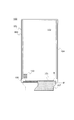
- the display device 100 includes a substrate 101, and on one surface thereof, various conductive layers patterned in a desired shape, a semiconductor layer, and an insulating layer.
- the plurality of pixels 103 are formed by the conductive layer, the semiconductor layer, and the insulating layer.
- a driver circuit (a gate driver circuit 104 and a source driver circuit 105) for driving the plurality of pixels 103 is formed on the substrate 101 simultaneously with the plurality of pixels 103 using the above conductive layer, semiconductor layer, and insulating layer.
- the IC may be mounted on one surface of the substrate 101.
- the plurality of pixels 103 are arranged, for example, in a matrix, and a collection of these forms a display area 102.
- the gate drive circuit 104 and the source drive circuit 105 are disposed in the peripheral area outside the display area 102. From the display area 102, the gate drive circuit 104, and the source drive circuit 105, various wirings (not shown) formed of a patterned conductive layer extend to one side of the substrate 101, and the respective wirings are at the edge of the substrate 101. It is electrically connected to the terminal 106 disposed nearby. These terminals 106 are connected to a flexible printed circuit (FPC) 107.
- FPC flexible printed circuit
- the driver circuit may be mounted not on the substrate 101 but on the FPC 107.
- a video signal and various control signals are supplied from an external controller (not shown) of the display device through the FPC 107, and the video signal is processed by the source drive circuit 105 and input to the plurality of pixels 103.
- Various control signals are input to the gate drive circuit 104 and the source drive circuit 105.
- Power for driving the gate driving circuit 104, the source driving circuit 105, and the plurality of pixels 103 is supplied to the display device 100 in addition to the video signal and various control signals.
- Each of the plurality of pixels 103 has a light emitting element described later. Part of the power supplied to the display device 100 is supplied to the light emitting element of each of the plurality of pixels 103 to cause the light emitting element to emit light.
- a bendable area 200 is provided over the entire display area 102, and an electronic device having high designability with the display surface having a curved surface shape, an electronic apparatus capable of storing the display area in a roll, etc. It becomes possible to apply to Further, as shown in FIGS. 3 and 4, the substrate 101 is bent in the direction of the arrow 301 in the bending area 300 provided between the display area 102 and the FPC 107, and the source drive circuit 105 and the FPC 107 are displayed in the display area 102. On the back side of the Thereby, narrowing of the display device 100 can be realized.
- FIG. 4 is shown in FIG. 4, and the substrate 101 is bent as shown by the arrow 301.
- the source drive circuit 105 and the FPC 107 are disposed so as to overlap on the back surface side of the display area 102, and the frame is narrowed as indicated by a width 302. Further, a spacer 303 for holding the cross-sectional shape of the substrate 101 may be provided inside the bent portion.
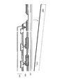
- FIG. 5 shows a cross-sectional configuration of the display device 100 according to an embodiment of the present invention.
- the substrate 101 is flexible and has a stacked structure including the first resin layer 501, the first inorganic insulating layer 502, the second inorganic insulating layer 503, and the second resin layer 504.
- the functional layer 505 including the gate driving circuit and the plurality of pixels formed using the conductive layer, the semiconductor layer, and the insulating layer is formed over the substrate 101 and sealed over the functional layer 505.
- Layer 506 is formed.
- the first resin layer 501 and the second resin layer 504 are configured as layers containing a material selected from, for example, acrylic, polyimide, polyethylene terephthalate, polyethylene naphthalate and the like.
- the first inorganic insulating layer 502 has a function as a barrier film to prevent moisture and other contaminants from entering the functional layer 505 through the first resin layer 501 and the second resin layer 504 as one of its functions.
- the second inorganic insulating layer 503 has, as one of its functions, a function to improve adhesion at the interface between the first inorganic insulating layer 502 and the second resin layer 504, and is amorphous silicon that has good adhesion to both materials. It is configured as a layer that contains.
- the resin layer and the inorganic insulating layer have different stresses remaining in the film due to the difference between the respective materials and the forming process thereof. As a result, the adhesion at the interface between the two deteriorates. Since the deterioration in adhesion is particularly remarkable when the resin layer is formed on the surface on which the inorganic insulating layer is formed, in the example of FIG.
- the second inorganic insulating layer 503 and the first inorganic insulating layer 502 Although provided between the second resin layer 504, it may be provided between the first resin layer 501 and the first inorganic insulating layer 502 for the same purpose, or may be omitted.
- the film thickness of the substrate 101 is such a thickness as to be compatible with flexibility such that it can be bent or bent as shown in FIGS. 2 to 4 and strength that does not cause breakage by bending. And preferably includes the above-described laminated structure, for example, 100 ⁇ m or less, and preferably 50 ⁇ m or less. More preferably, it can be about 10 ⁇ m to 30 ⁇ m.
- the film thickness of the first resin layer 501 is thinner than the film thickness of the second resin layer 504.
- the film thickness of the first resin layer 501 is preferably 70% or less, preferably about 40% to 60%, of the film thickness of the second resin layer 504.
- the film thickness of the first resin layer 501 is about 50% of the film thickness of the second resin layer 504.
- the material forming the first resin layer 501 is formed on one surface of a supporting substrate or the like by a coating method or the like and then fired. Subsequently, the first inorganic insulating layer 502 and the second inorganic insulating layer 503 are formed respectively by vapor deposition such as the CVD method, and further, the material constituting the second resin layer 504 is formed by the coating method or the like. The process of baking is implemented. Here, at the time of firing of the second resin layer 504, the first resin layer 501 is also heated at the same time, so that the gas component is also released from the first resin layer 501.
- the desorbed gas component stays near the interface between the first resin layer 501 and the first inorganic insulating layer 502. . Thereby, peeling of the interface between the first resin layer 501 and the first inorganic insulating layer 502 may occur.
- the first resin layer 501 and the second resin layer 504 are each fired at about 450 ° C. to 500 ° C., but the maximum value of the firing temperature of the second resin layer 504 is the firing temperature of the first resin layer 501. Set so as not to exceed the maximum value.
- the first resin layer 501 is also simultaneously heated when the second resin layer 504 is fired, but the first resin layer 501 is not heated unless it reaches the maximum firing temperature when the first resin layer 501 is fired in advance. There is little desorption of gas components from the resin layer 501.
- the first resin layer 501 does not have its heating history, so that desorption of new gas components occurs. That is, by setting the maximum value of the baking temperature of the second resin layer 504 not to exceed the maximum value of the baking temperature of the first resin layer 501, the first resin layer 501 at the time of baking the second resin layer 504. It is possible to suppress gas component desorption from
- Polyimide is applied and formed on a supporting substrate, and then fired at a maximum temperature of 500 ° C. to obtain a 7 ⁇ m thick polyimide layer as the first resin layer 501.
- a silicon oxide film is formed to a thickness of 600 nm by the CVD method as the first inorganic insulating layer 502, and an amorphous silicon film is formed to a thickness of 10 nm by the CVD method as the second inorganic insulating layer 503.
- polyimide is applied and formed, and then firing is performed at a maximum temperature of 480 ° C. to obtain a 13 ⁇ m thick polyimide layer as the second resin layer 504.
- the flexible substrate 101 is formed. According to the above-described process, a favorable laminated structure can be obtained without causing peeling of the first inorganic insulating layer 502 caused by the gas desorbed from the first resin layer 501 when the second resin layer 504 is fired.
- the first resin layer 501 and the second resin layer 504 are both formed of a 10 ⁇ m thick polyimide layer as shown in FIG. 6B under the above conditions as a comparative example, the first resin layer 501 and the first resin layer A peeling 601 was generated between the first inorganic insulating layer 502 and the first inorganic insulating layer 502.
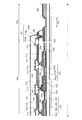
- FIG. 7 schematically shows a B-B 'cross-sectional structure of the display device 100 in FIG. Mainly, an N-channel thin film transistor (hereinafter referred to as a "TFT" that constitutes a pixel. Also, when the TFT is an N-channel type, it is called “NchTFT”, and when it is a P-channel type, it is called “PchTFT” And a bent area for bending a frame area including the display area including the terminal area, the terminal area, and the terminal area.
- NchTFT N-channel thin film transistor
- the silicon oxide film 701 a as the undercoat layer 701 is formed on the substrate 101 having a laminated structure including the first resin layer 501, the first inorganic insulating layer 502, the second inorganic insulating layer 503, and the second resin layer 504.
- a three-layer stacked structure of a silicon nitride film 701b and a silicon oxide film 701c is provided.
- the lowermost silicon oxide film 701a is for improving adhesion with the substrate 101
- the middle silicon nitride film 701b is used as a block film of moisture and impurities from the outside
- the uppermost silicon oxide film 701c is a silicon nitride film 701b.
- it is not limited to this structure.
- the light shielding layer (Light Shield layer: LS layer) 702 may be formed in accordance with a portion where a TFT is to be formed later.
- the LS layer 702 suppresses the change in TFT characteristics due to the infiltration of light from the back surface of the channel of the TFT or the like, and the LS layer 702 is formed of a conductive layer to apply a predetermined potential, thereby giving the TFT a back gate effect. It can be given.
- the LS layer 702 is formed in an island shape in accordance with the portion where the driving transistor (DRT) is to be formed.
- a silicon nitride film 701 b and a silicon oxide film 701 c are stacked to form an LS layer 702 in the undercoat layer 701.
- the embodiment of the present invention is not limited to this, and the LS layer 702 may be formed on the substrate 101 first, and then the undercoat layer 701 may be formed.
- the TFT 703 is formed on the undercoat layer 701. Although a polysilicon TFT is taken as an example of the TFT 703 and only the Nch TFT is shown here, a Pch TFT may be formed simultaneously.
- the Nch TFT has a structure in which a low concentration impurity region is provided between the channel region and the source / drain region (high concentration impurity region).
- a silicon oxide film is used as the gate insulating film 704, and the gate electrode 705 is a MoW film (first wiring layer).
- the first wiring layer forms a storage capacitance line in addition to the gate electrode 705 of the TFT 703, and is also used to form a storage capacitance (Cs) 707 with the polysilicon 706.
- a silicon nitride film or a silicon oxide film to be an interlayer insulating film 708 is stacked on the TFT 703, and then patterning is performed to form a contact hole reaching the polysilicon 706 or the like.
- the interlayer insulating film 708 in a portion corresponding to the bent region 750 is removed.
- the undercoat layer 701 is exposed by the removal of the interlayer insulating film 708, it is also patterned and removed.
- the second resin layer 504 that constitutes the substrate 101 is exposed. At this time, although not shown in particular, the surface of the second resin layer 504 may be partially corroded through etching of the undercoat layer 701 to cause film reduction.
- a conductive layer (second wiring layer) 709 to be a source / drain electrode and a lead wiring is formed.
- a three-layer laminated structure of Ti, Al, and Ti was adopted.
- a part of the capacitance (Cs) 707 is formed.
- the lead wiring extends to the end of the peripheral edge of the substrate, and forms a terminal 106 for connecting a flexible printed circuit or a drive IC later.
- the terminal 106 may be formed in the same layer as the first wiring layer forming the gate electrode 705.
- planarization film 710 is formed to cover the TFT 703 and the lead wiring.
- organic materials such as photosensitive acrylic and polyimide are often used.
- the surface flatness is superior to that of an inorganic insulating material formed by CVD or the like.
- the planarization film 710 is removed in the pixel contact portion and a part of the peripheral region 770.
- a portion where the conductive layer 709 is exposed by removal of the planarizing film is once covered with a transparent conductive film 711.
- the transparent conductive film 711 for example, ITO (Indium tin oxide) is used.
- the transparent conductive film 711 is once covered with a silicon nitride film 712, and the pixel contact portion is reopened to form a conductive layer 713 to be a pixel electrode.
- the pixel electrode is formed as a reflective electrode, and has a three-layer laminated structure of IZO, Ag, and IZO.
- a storage capacitance (Cad) 714 is formed by the transparent conductive film 711, the silicon nitride film 712, and the conductive layer 713.
- the transparent conductive film 711 is also formed on the surface of the terminal 106.
- One purpose of the transparent conductive film on the terminal 106 is to provide it as a barrier film so that the wiring exposed portion is not damaged in the subsequent steps.
- the transparent conductive film 711 is partially exposed to the etching environment at the time of patterning of the pixel electrode (conductive layer 713), the transparent conductive film 711 is transparent conductive by the annealing process performed from the formation of the transparent conductive film 711 to the formation of the conductive layer 713.
- the film 711 has sufficient resistance to the etching of the conductive layer 713.
- an insulating layer called a bank (rib) 715 which serves as a partition in the pixel region is formed.
- a bank (rib) 715 an organic material such as photosensitive acrylic or polyimide is used as in the case of the flattening film 710.
- the bank 715 is preferably opened so as to expose the pixel electrode surface as a light emitting area, and the open end thereof preferably has a gentle tapered shape. If the opening end has a sharp shape, coverage failure of the organic layer to be formed later will occur.
- the planarizing film 710 and the bank 715 have portions that are in contact with each other through the openings 716 provided in the silicon nitride film 712 between them.
- This is an opening for extracting moisture and gas desorbed from the planarizing film 710 through the bank 715 through heat treatment or the like after formation of the bank.
- the moisture and gas desorbed here are the same phenomena as those desorbed from the first resin layer 501 and the second resin layer 504 at the time of formation of the substrate 101 described above, and the bank from the planarization film 710 through the opening 716 By pulling out to 715, peeling of the interface between the planarization film 710 and the silicon nitride film 712 can be suppressed.
- an organic layer 717 for forming an organic EL layer is stacked.
- a hole transport layer, a light emitting layer, and an electron transport layer are stacked in order from the pixel electrode side.
- These layers may be formed by vapor deposition, or may be formed by coating on a solvent dispersion. Further, as shown in FIG. 7, it may be selectively formed for each pixel, or may be formed solidly on the entire surface covering the display area. In the case of solid formation, white light can be obtained at all pixels, and a desired color wavelength portion can be extracted by a color filter (not shown).
- a counter electrode 718 is formed.
- the counter electrode 718 needs to be light transmissive.
- the top emission structure is a structure in which light is emitted from the counter electrode 718 disposed on the substrate 101 with the organic layer 717 interposed therebetween.
- an MgAg film is formed as the counter electrode 718 as a thin film to which the light emitted from the organic EL layer can be transmitted.
- the pixel electrode side becomes an anode and the counter electrode side becomes a cathode.
- the counter electrode 718 is formed over the display region 760 and the cathode contact portion 780 provided in the vicinity of the display region, is connected to the lower conductive layer 709 at the cathode contact portion 780, and is finally drawn out to the terminal 106.
- a sealing layer 719 is formed.
- the sealing layer 719 has one of the functions to prevent the intrusion of moisture from the outside as one of the functions of the previously formed organic layer, and the sealing layer is required to have high gas barrier properties.
- a structure in which a silicon nitride film 719a, an organic resin 719b, and a silicon nitride film 719c are stacked is shown as a stacked structure including a silicon nitride film as the sealing layer 719.
- an amorphous silicon layer may be provided between the silicon nitride film 719a and the organic resin 719b for the purpose of improving the adhesion as described in the lamination step of the substrate 101.
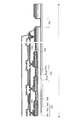
- the display device 100 is manufactured by the above steps. If necessary, as shown in FIG. 8, a cover glass 800 may be provided on the sealing layer 719. A touch sensor or the like may be formed on the cover glass 800. In this case, in order to fill the space between the display device 100 and the cover glass 800, a filler 810 using a resin or the like may be interposed.
- the inorganic insulating layer or the like Since the inorganic insulating layer or the like has poor toughness particularly when the substrate 101 is bent, the inorganic insulating layer is removed in the bent region 750 because cracks are easily generated.
- a resin coat 820 or the like may be provided on the conductive layer 709 so as to cover the bent region 750.
- the gas component from the first resin layer can be obtained. Minimize detachment. Further, the maximum value of the temperature at the heat treatment of the second resin layer 504 is set so as not to exceed the maximum value of the temperature at the heat treatment of the first resin layer 501. In this manner, desorption of gas components from the first resin layer 501 can be suppressed at the time of firing of the second resin layer 504. Thus, peeling can be suppressed at the interface between the first resin layer 501 and the first inorganic insulating layer 502.
- a first inorganic insulating layer 502 is provided between the first resin layer 501 and the second resin layer 504.
- a second inorganic insulating layer 503 is provided between the first resin layer 501 and the first inorganic insulating layer 502 or between the first inorganic insulating layer 502 and the second resin layer 504.
- the inorganic insulating layer in the bending region 750, a region for removing the inorganic insulating layer (undercoat layer 701, gate insulating film 704, interlayer insulating film 708) provided above the substrate 101 is provided, and The first inorganic insulating layer 502 and the second inorganic insulating layer 503 provided between the resin layer 501 and the second resin layer 504 extend to the bent region 750.
- the inorganic insulating layer can be configured not to extend.
- the conductive layer 709 is provided in contact with the first resin layer 501.
- the first resin layer 501 has a smaller thickness than the second resin layer 504, so the bending region 750 after removing the second resin layer 504 has a mechanical strength. Is lower. Therefore, providing a resin coat 820 as shown in FIG. 8 is very effective.
- the substrate 101 can be favorably bent by forming the inorganic insulating layer in the bent region 750 so as not to extend.
- mechanical strength in the bending region 750 can be improved by providing the resin coat 820 after bending the substrate 101 in the bending region 750.
- a display device which can maintain high reliability even when the flexible substrate 101 is bent or bent can be provided.
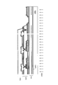
- Embodiment 3 When the substrate 101 is a flexible material, it is difficult to maintain the flatness of the substrate 101 through the steps described with reference to FIGS. 7 to 9. Therefore, when forming such a display device, as shown in FIG. 10A, the first resin layer 501, the first inorganic insulating layer 502, and the second inorganic insulating layer are formed on a supporting substrate 1001 made of glass or quartz. A substrate 101 including the third resin layer 503 and the second resin layer 504 is formed. Subsequently, a functional layer 505 including a plurality of pixels formed using a conductive layer, a semiconductor layer, and an insulating layer, and a gate driving circuit is formed.
- a sealing layer 506 including a silicon nitride film 719a, an organic resin 719b, and a silicon nitride film 719c is formed.
- the planarity over the substrate 101 is maintained by the supporting substrate 1001, so that the manufacturing process including high-precision photolithography can be completed successfully.
- the first embodiment can be referred to for the details of the method for forming the sealing layer 506 from the substrate 101.
- laser irradiation processing 1002 and the like are performed from the side of the support substrate 1001 where the substrate 101 is not formed.
- the laser irradiation processing 1002 a portion 1003 of the first resin layer 501 of the substrate 101 in contact with the support substrate 1001 is altered, and the adhesion is lowered. This decrease in adhesion is caused by the first resin layer 501 partially causing ablation or shrinking due to heat.
- the display device 100 peeled off from the support substrate 1001 can take the form shown in FIGS. 2 to 4 due to the flexibility of the substrate 101 at this point.
- the semiconductor layer, the insulating layer, and the conductive layer can be processed with high accuracy.
Landscapes
- Engineering & Computer Science (AREA)
- Manufacturing & Machinery (AREA)
- Microelectronics & Electronic Packaging (AREA)
- Physics & Mathematics (AREA)
- General Physics & Mathematics (AREA)
- Theoretical Computer Science (AREA)
- Optics & Photonics (AREA)
- Electroluminescent Light Sources (AREA)
- Devices For Indicating Variable Information By Combining Individual Elements (AREA)
Priority Applications (1)
| Application Number | Priority Date | Filing Date | Title |
|---|---|---|---|
| US16/846,478 US11258022B2 (en) | 2017-10-23 | 2020-04-13 | Manufacturing method of display device |
Applications Claiming Priority (2)
| Application Number | Priority Date | Filing Date | Title |
|---|---|---|---|
| JP2017-204545 | 2017-10-23 | ||
| JP2017204545A JP7064846B2 (ja) | 2017-10-23 | 2017-10-23 | 表示装置及び表示装置の製造方法 |
Related Child Applications (1)
| Application Number | Title | Priority Date | Filing Date |
|---|---|---|---|
| US16/846,478 Continuation US11258022B2 (en) | 2017-10-23 | 2020-04-13 | Manufacturing method of display device |
Publications (1)
| Publication Number | Publication Date |
|---|---|
| WO2019082847A1 true WO2019082847A1 (ja) | 2019-05-02 |
Family
ID=66246557
Family Applications (1)
| Application Number | Title | Priority Date | Filing Date |
|---|---|---|---|
| PCT/JP2018/039202 Ceased WO2019082847A1 (ja) | 2017-10-23 | 2018-10-22 | 表示装置及び表示装置の製造方法 |
Country Status (3)
| Country | Link |
|---|---|
| US (1) | US11258022B2 (https=) |
| JP (1) | JP7064846B2 (https=) |
| WO (1) | WO2019082847A1 (https=) |
Cited By (1)
| Publication number | Priority date | Publication date | Assignee | Title |
|---|---|---|---|---|
| JP2021105704A (ja) * | 2019-12-26 | 2021-07-26 | Tianma Japan株式会社 | 表示装置 |
Families Citing this family (12)
| Publication number | Priority date | Publication date | Assignee | Title |
|---|---|---|---|---|
| CN109755256B (zh) | 2017-11-01 | 2022-01-11 | 京东方科技集团股份有限公司 | 柔性显示面板及制备方法、柔性显示装置 |
| KR102536257B1 (ko) * | 2018-01-25 | 2023-05-24 | 삼성디스플레이 주식회사 | 표시 장치 |
| WO2019176113A1 (ja) * | 2018-03-16 | 2019-09-19 | シャープ株式会社 | 表示デバイス、表示デバイスの製造方法、表示デバイスの製造装置 |
| US11508921B2 (en) * | 2018-03-20 | 2022-11-22 | Sharp Kabushiki Kaisha | Display device and method for manufacturing same where a resin layer containing air bubbles |
| US11380222B2 (en) * | 2018-03-27 | 2022-07-05 | Sharp Kabushiki Kaisha | Display device |
| KR102754154B1 (ko) * | 2019-08-05 | 2025-01-10 | 엘지디스플레이 주식회사 | 표시 장치 |
| JP7680372B2 (ja) * | 2019-12-20 | 2025-05-20 | 京東方科技集團股▲ふん▼有限公司 | フレキシブル表示パネル及びその製造方法、並びにフレキシブル表示装置 |
| KR102752245B1 (ko) * | 2019-12-31 | 2025-01-10 | 엘지디스플레이 주식회사 | 전계발광 표시장치 및 그의 제조방법 |
| CN115428059B (zh) * | 2020-04-20 | 2025-08-05 | 夏普株式会社 | 显示装置和显示装置的制造方法 |
| US12484399B2 (en) | 2020-04-21 | 2025-11-25 | Sharp Kabushiki Kaisha | Display device and method for manufacturing display device |
| CN116745836A (zh) * | 2021-01-14 | 2023-09-12 | 株式会社半导体能源研究所 | 显示装置及电子设备 |
| US12278220B2 (en) | 2021-06-25 | 2025-04-15 | Boe Technology Group Co., Ltd. | Driving substrate, light-emitting apparatus and manufacturing method thereof, and splicing display apparatus each having driving substrate in bending area |
Citations (5)
| Publication number | Priority date | Publication date | Assignee | Title |
|---|---|---|---|---|
| JP2014232300A (ja) * | 2013-05-28 | 2014-12-11 | エルジー ディスプレイ カンパニー リミテッド | フレキシブル表示装置及びその製造方法 |
| US20160141551A1 (en) * | 2014-11-17 | 2016-05-19 | Samsung Display Co., Ltd. | Organic light-emitting diode (oled) display, electronic device including the same, and method of manufacturing the oled display |
| US20160174304A1 (en) * | 2014-12-10 | 2016-06-16 | Lg Display Co., Ltd. | Flexible display device with multiple types of micro-coating layers |
| JP2017111435A (ja) * | 2015-12-15 | 2017-06-22 | エルジー ディスプレイ カンパニー リミテッド | フレキシブル表示装置 |
| US20170288007A1 (en) * | 2016-03-31 | 2017-10-05 | Samsung Display Co., Ltd. | Display device and manufacturing method thereof that may minimize an occurrence of a defect in the display device |
Family Cites Families (6)
| Publication number | Priority date | Publication date | Assignee | Title |
|---|---|---|---|---|
| JP5720222B2 (ja) | 2010-12-13 | 2015-05-20 | ソニー株式会社 | 表示装置及び電子機器 |
| CN105552247B (zh) * | 2015-12-08 | 2018-10-26 | 上海天马微电子有限公司 | 复合基板、柔性显示装置及其制备方法 |
| KR102405120B1 (ko) * | 2016-09-29 | 2022-06-08 | 삼성디스플레이 주식회사 | 표시 장치 및 표시 장치의 제조방법 |
| KR102631989B1 (ko) * | 2016-10-31 | 2024-01-31 | 엘지디스플레이 주식회사 | 유기발광 표시장치 및 그 제조방법 |
| WO2019026280A1 (ja) * | 2017-08-04 | 2019-02-07 | シャープ株式会社 | 樹脂基板および表示デバイス |
| JP2019124811A (ja) * | 2018-01-16 | 2019-07-25 | 株式会社ジャパンディスプレイ | 表示装置及び表示装置の製造方法 |
-
2017
- 2017-10-23 JP JP2017204545A patent/JP7064846B2/ja active Active
-
2018
- 2018-10-22 WO PCT/JP2018/039202 patent/WO2019082847A1/ja not_active Ceased
-
2020
- 2020-04-13 US US16/846,478 patent/US11258022B2/en active Active
Patent Citations (5)
| Publication number | Priority date | Publication date | Assignee | Title |
|---|---|---|---|---|
| JP2014232300A (ja) * | 2013-05-28 | 2014-12-11 | エルジー ディスプレイ カンパニー リミテッド | フレキシブル表示装置及びその製造方法 |
| US20160141551A1 (en) * | 2014-11-17 | 2016-05-19 | Samsung Display Co., Ltd. | Organic light-emitting diode (oled) display, electronic device including the same, and method of manufacturing the oled display |
| US20160174304A1 (en) * | 2014-12-10 | 2016-06-16 | Lg Display Co., Ltd. | Flexible display device with multiple types of micro-coating layers |
| JP2017111435A (ja) * | 2015-12-15 | 2017-06-22 | エルジー ディスプレイ カンパニー リミテッド | フレキシブル表示装置 |
| US20170288007A1 (en) * | 2016-03-31 | 2017-10-05 | Samsung Display Co., Ltd. | Display device and manufacturing method thereof that may minimize an occurrence of a defect in the display device |
Cited By (2)
| Publication number | Priority date | Publication date | Assignee | Title |
|---|---|---|---|---|
| JP2021105704A (ja) * | 2019-12-26 | 2021-07-26 | Tianma Japan株式会社 | 表示装置 |
| JP7499089B2 (ja) | 2019-12-26 | 2024-06-13 | Tianma Japan株式会社 | 表示装置 |
Also Published As
| Publication number | Publication date |
|---|---|
| US11258022B2 (en) | 2022-02-22 |
| JP7064846B2 (ja) | 2022-05-11 |
| JP2019078847A (ja) | 2019-05-23 |
| US20200243782A1 (en) | 2020-07-30 |
Similar Documents
| Publication | Publication Date | Title |
|---|---|---|
| WO2019082847A1 (ja) | 表示装置及び表示装置の製造方法 | |
| US10809553B2 (en) | Flexible substrate | |
| TWI570493B (zh) | 顯示裝置和製造其之方法 | |
| CN103389605B (zh) | 显示装置 | |
| JP5253686B2 (ja) | アクティブマトリクス基板、表示装置、およびアクティブマトリクス基板の製造方法 | |
| WO2019012769A1 (ja) | 表示装置、および表示装置の製造方法 | |
| WO2019012768A1 (ja) | 表示装置 | |
| CN114256328A (zh) | 薄膜晶体管基板和显示装置 | |
| WO2012144165A1 (ja) | 薄膜トランジスタ、表示パネル及び薄膜トランジスタの製造方法 | |
| CN110021631A (zh) | 显示装置及其制造方法 | |
| JP6726973B2 (ja) | 表示装置 | |
| WO2011142064A1 (ja) | アクティブマトリクス基板及び表示パネル | |
| US12108624B2 (en) | Display device including bending region including laminated first and second resin layers | |
| CN111656427B (zh) | 显示装置 | |
| JP2019095507A (ja) | 表示装置 | |
| CN106067471A (zh) | 显示装置及其制造方法 | |
| WO2015087466A1 (ja) | 薄膜トランジスタ基板及び薄膜トランジスタ基板の製造方法 | |
| WO2019049461A1 (ja) | 表示装置、および表示装置の製造方法 | |
| WO2017195699A1 (ja) | アクティブマトリクス基板、その製造方法および表示装置 | |
| CN110832626B (zh) | 可挠性显示装置 | |
| JP5964967B2 (ja) | 半導体装置およびその製造方法 | |
| KR20150121410A (ko) | 반도체 박막 트랜지스터, 반도체 박막 트랜지스터 제조방법, 어레이 기판 및 표시장치 |
Legal Events
| Date | Code | Title | Description |
|---|---|---|---|
| 121 | Ep: the epo has been informed by wipo that ep was designated in this application |
Ref document number: 18871177 Country of ref document: EP Kind code of ref document: A1 |
|
| NENP | Non-entry into the national phase |
Ref country code: DE |
|
| 122 | Ep: pct application non-entry in european phase |
Ref document number: 18871177 Country of ref document: EP Kind code of ref document: A1 |