WO2019078271A1 - 電気部品用ソケット - Google Patents
電気部品用ソケット Download PDFInfo
- Publication number
- WO2019078271A1 WO2019078271A1 PCT/JP2018/038707 JP2018038707W WO2019078271A1 WO 2019078271 A1 WO2019078271 A1 WO 2019078271A1 JP 2018038707 W JP2018038707 W JP 2018038707W WO 2019078271 A1 WO2019078271 A1 WO 2019078271A1
- Authority
- WO
- WIPO (PCT)
- Prior art keywords
- contact
- sheet member
- socket
- insertion portion
- contactor
- Prior art date
- Legal status (The legal status is an assumption and is not a legal conclusion. Google has not performed a legal analysis and makes no representation as to the accuracy of the status listed.)
- Ceased
Links
Images
























Classifications
-
- G—PHYSICS
- G01—MEASURING; TESTING
- G01R—MEASURING ELECTRIC VARIABLES; MEASURING MAGNETIC VARIABLES
- G01R1/00—Details of instruments or arrangements of the types included in groups G01R5/00 - G01R13/00 and G01R31/00
- G01R1/02—General constructional details
- G01R1/04—Housings; Supporting members; Arrangements of terminals
- G01R1/0408—Test fixtures or contact fields; Connectors or connecting adaptors; Test clips; Test sockets
- G01R1/0433—Sockets for IC's or transistors
- G01R1/0441—Details
- G01R1/0466—Details concerning contact pieces or mechanical details, e.g. hinges or cams; Shielding
-
- G—PHYSICS
- G01—MEASURING; TESTING
- G01R—MEASURING ELECTRIC VARIABLES; MEASURING MAGNETIC VARIABLES
- G01R1/00—Details of instruments or arrangements of the types included in groups G01R5/00 - G01R13/00 and G01R31/00
- G01R1/02—General constructional details
- G01R1/04—Housings; Supporting members; Arrangements of terminals
- G01R1/0408—Test fixtures or contact fields; Connectors or connecting adaptors; Test clips; Test sockets
- G01R1/0433—Sockets for IC's or transistors
- G01R1/0483—Sockets for unleaded IC's having matrix type contact fields, e.g. BGA or PGA devices; Sockets for unpackaged, naked chips
-
- G—PHYSICS
- G01—MEASURING; TESTING
- G01R—MEASURING ELECTRIC VARIABLES; MEASURING MAGNETIC VARIABLES
- G01R31/00—Arrangements for testing electric properties; Arrangements for locating electric faults; Arrangements for electrical testing characterised by what is being tested not provided for elsewhere
- G01R31/26—Testing of individual semiconductor devices
-
- G—PHYSICS
- G01—MEASURING; TESTING
- G01R—MEASURING ELECTRIC VARIABLES; MEASURING MAGNETIC VARIABLES
- G01R31/00—Arrangements for testing electric properties; Arrangements for locating electric faults; Arrangements for electrical testing characterised by what is being tested not provided for elsewhere
- G01R31/28—Testing of electronic circuits, e.g. by signal tracer
- G01R31/2851—Testing of integrated circuits [IC]
- G01R31/2886—Features relating to contacting the IC under test, e.g. probe heads; chucks
-
- H—ELECTRICITY
- H01—ELECTRIC ELEMENTS
- H01R—ELECTRICALLY-CONDUCTIVE CONNECTIONS; STRUCTURAL ASSOCIATIONS OF A PLURALITY OF MUTUALLY-INSULATED ELECTRICAL CONNECTING ELEMENTS; COUPLING DEVICES; CURRENT COLLECTORS
- H01R33/00—Coupling devices specially adapted for supporting apparatus and having one part acting as a holder providing support and electrical connection via a counterpart which is structurally associated with the apparatus, e.g. lamp holders; Separate parts thereof
- H01R33/74—Devices having four or more poles, e.g. holders for compact fluorescent lamps
- H01R33/76—Holders with sockets, clips, or analogous contacts adapted for axially-sliding engagement with parallely-arranged pins, blades, or analogous contacts on counterpart, e.g. electronic tube socket
Definitions
- the present invention relates to an electrical component socket electrically connected to an electrical component such as a semiconductor device (hereinafter referred to as "IC package").
- IC package electrical component such as a semiconductor device
- an IC socket in which a contact pin is disposed is known as a socket for electrical components of this type.
- the IC socket is disposed on the wiring board and is adapted to receive the IC package to be inspected.
- the terminals of the IC package and the electrodes of the wiring board are electrically connected through the contact pins. Are connected to perform a test such as a continuity test.
- the contact pin of such an IC socket is known to be provided with a coil spring between two contacts, and is biased in a direction in which the two contacts are separated by the biasing force of this coil spring. (See, for example, Patent Document 1). Then, by pressing the two contacts in a direction approaching each other against the biasing force of the coil spring with the terminals of the IC package and the electrodes of the wiring board, the terminals of the IC package and the electrodes of the wiring board are It is comprised so that it may be electrically connected with predetermined
- this invention makes it a subject to provide the socket for electrical components which can simplify a structure and can aim at cost reduction.
- an electrical component socket is disposed between the first electrical component and the opposing second electrical component, and electrically connects the first electrical component and the second electrical component.
- a socket for an electrical component comprising: a sheet member made of an insulator having an elastic force; and a first contact disposed on a first surface side of the sheet member on the first electrical component side and contacting the first electrical component And a first contactor having a first insertion portion inserted into the sheet member continuously from the first contact portion, and a second contact side of the sheet member on the second electric component side
- a second contact portion having a second contact portion contacting the second electric component and a second contact portion having a second insertion portion continuously inserted into the sheet member from the second contact portion, the first insertion portion And the second insertion portion are disposed in contact with each other, and the first The sheet member is deformed by the contact portion and the second contact portion being pressed in the direction approaching each other, and the slide is performed in a state where the first insertion portion and the second insertion portion are electrically
- the first contactor has the first contact portion abutting on the first surface, and the sheet member is pressed by the first electric component when the first contact portion is pressed by the first electric component.
- the first contactor may be characterized in that it is configured to be elastically deformed by being pressed by the contact portion.
- the first insertion portion is formed in a substantially rod shape
- the second insertion portion is formed in a substantially cylindrical shape
- the first insertion portion is inserted into the second insertion portion.
- the socket may be characterized in that it is a socket for an electric component configured to slide in a contact state.
- the first insertion portion and the second insertion portion are formed in a substantially rod shape, and are configured to slide in a state in which the side surfaces of the first insertion portion and the second insertion portion are in contact with each other. It may be characterized by being a socket for electrical components.
- the sheet member has two members of a first sheet member and a second sheet member, and the first contactor and the second contact with the first sheet member and the second sheet member. It may be a socket for electrical parts in which a child is disposed.
- the sheet member penetrates between the first surface on the first electric component side and the second surface on the second electric component side, and the first insertion portion and the second insertion portion are inserted.
- a projecting portion protruding in a direction intersecting with the through hole is provided in at least one of the first insertion portion and the second inserting portion, and intersects with the through hole. The projection may be in pressure contact with the other contact by an elastic force of the sheet member acting in a direction.
- the second contact may have a second contact portion that contacts a step provided in the through hole.
- a cross-sectional shape in which the second insertion portion intersects the through hole is formed in an arc piece shape, and the first insertion portion is formed in a substantially rod shape, and the inner side of the second insertion portion May be inserted into the
- the second contact includes a pair of the second insertion portions extending along the through hole, facing each other, and a second connection portion connecting the second insertion portions.
- the first insertion portion of the first contact may be inserted and held between the second insertion portions.
- the edge of the sheet member may be fixed to a fixing plate harder than the sheet member.
- the sheet member is formed in a band shape having a thickness capable of accommodating the first insertion portion and the second insertion portion, and both sides of the sheet member are fixed to the fixing plate. It may be a feature.
- the strip-like sheet member in which a plurality of the first contacts and the second contacts are disposed is formed substantially in a substantially frame shape over substantially the whole, and the fixing plate is disposed outside the sheet member. It may be characterized by having a part and an inner part arranged inside the sheet member.
- the outer side portion and the inner side portion of the fixing plate may be connected to each other by a connecting portion or may be separated separately.
- the sheet member may have an inner opening, and the fixing plate may be disposed at least in the inner opening.
- the socket for electrical parts of the present invention since the first contactor and the second contactor are inserted so as to be in contact with each other from the mutually facing surfaces of the sheet member made of the elastic insulator, The sheet member is deformed by pressing the first contactor and the second contactor with the electric component and the second electric component, and the elastic force is used to make a predetermined contact between the first electric component and the second electric component. It can be connected electrically with pressure. As a result, it is not necessary to separately provide a biasing member such as a coil spring, which is conventionally required, and the number of parts can be reduced to reduce the cost of the socket for electrical parts.
- a biasing member such as a coil spring
- the first contact part has a first contact portion which abuts on the first surface, and the first contact part is pressed by the first electric component, whereby the sheet member is If the first contact portion is configured to be elastically deformed by being pressed by the contact portion, the first contact portion can be brought into contact with the first electric component by a reaction force of the sheet member, and the biasing means is separately
- the structure can be simplified without the need for providing.
- the first insertion portion of the first contact is configured to slide while being inserted into and in contact with the inside of the second insertion portion of the second contact. Therefore, the first contact portion of the first contactor and the second contact portion of the second contactor can be disposed substantially coaxially, and as a result, the first electric component and the second electric component face each other without shifting. Can be placed at approximately the same position.
- the first insertion portion of the first contact and the second insertion portion of the second contact are both formed substantially in a bar shape, and the side surfaces are in contact with each other Since it is configured to slide, the first contact and the second contact can be made into a simpler shape, and as a result, the manufacturing cost of the socket for electrical parts can be further reduced.
- the sheet member has two members of the first sheet member and the second sheet member, and the first contact member and the first sheet member are attached to the first sheet member and the second sheet member. Since the two contacts are disposed, the elastic force can be changed between the first sheet member and the second sheet member, and as a result, when the contact pressure to the first electric component and the second electric component is obtained, the freedom is obtained. You can raise the degree.
- the sheet member has the through hole in which the first insertion portion and the second insertion portion are inserted, and the protrusion provided on at least one of the contacts is the elastic force of the sheet member At the other contact. Therefore, the first contactor and the second contactor can be reliably brought into contact in the through hole. As a result, it is not necessary to individually provide a structure for bringing the first contact and the second contact into contact with each other, the connection structure between the first electric component and the second electric component can be simplified, and the cost can be reduced. Can be
- the second contact has the second contact portion to be in contact with the step provided in the through hole, the second contact is The second contact can be stably held in pressure contact with the second electric component.
- the cross-sectional shape intersecting the through hole is formed in an arc piece shape
- the first insertion portion is formed in a substantially rod shape, and a second insertion in an arc piece shape
- the first insertion portion of the first contactor can be reliably disposed inside the second insertion portion of the second contactor in the through hole if it is inserted inside the portion, and the first contactor and the second contactor Can be reliably brought into contact with each other.
- the second contacts have a pair of second insertion parts extending along the through hole facing each other, and the first insertion part of the first contact is the second insertion
- the first insertion portion of the first contact is brought into strong contact with the second insertion portion of the second contact in the through hole if it is inserted and held between the parts, the first contact and the second It is possible to reliably connect the contacts.
- the edge of the sheet member is fixed to the fixing plate harder than the sheet member, the edge of the sheet member having elastic force can be firmly supported non-displaceably. Therefore, distortion and deformation of the sheet member can be suppressed by the fixing plate, and the positional accuracy of the portion where the first contactor and the second contactor are inserted and arranged in the sheet member can be secured. For example, even if shrinkage occurs due to hardening or solidification when the sheet member is formed, it is possible to ensure the positional accuracy of the edge of the sheet member fixed to the fixing plate. As a result, the first contactor and the second contactor can be arranged on the sheet member with high accuracy.
- the sheet member is formed in a band shape having a thickness capable of accommodating the first insertion portion and the second insertion portion, and both sides of the sheet member are fixed to the fixing plate Therefore, it can be firmly supported non-displaceably on both sides, and when the sheet member shrinks, tension acts evenly from both sides. As a result, it is possible to prevent the sheet member from being distorted to one side, and it is possible to improve the positional accuracy of the arrangement portion of the first contactor and the second contactor in the sheet member.
- a band-like sheet member in which a plurality of first and second contacts are disposed substantially all over is formed in a substantially frame shape, and a fixing plate is disposed outside the sheet member And an inner portion disposed inside. Therefore, the outer edge and the inner edge of the fixing plate can firmly support the inner edge and the outer edge of the substantially frame-like sheet member in a non-displaceable manner, and when the sheet member shrinks The tension acts from both sides in a balanced manner.
- the substantially frame-shaped sheet member can be prevented from contracting and distorting to one side of the outer side and the inner side, and the positional accuracy of the arrangement portion of the first contactor and the second contactor in the substantially frame-shaped sheet member It can improve.
- the socket for electrical parts of the present invention for example, if the outer side and the inner side of the fixing plate are connected to each other by the connecting portion, the relative position between the outer side and the inner side can be reliably maintained by the connecting portion. . Therefore, both sides of the inner edge and the outer edge of the substantially frame-shaped sheet member can be reliably fixed at predetermined positions, and the positional accuracy of the arrangement positions of the first contactor and the second contactor in the substantially frame-shaped sheet member It can improve more.
- the tension of the resin sheet disposed between the outer side and the inner side can be evenly distributed over the entire frame. Therefore, it is possible to equalize the tension acting on the plurality of first contacts and the second contacts in the sheet member and to easily secure the positional accuracy.
- the socket for electrical parts of the present invention for example, since the sheet member has the inner opening and the fixing plate is disposed in the inner opening, a large amount of elastic material constituting the sheet member is provided inside the sheet member. It does not exist, and tension does not act due to shrinkage or the like when forming the elastic material.
- the fixing plate can firmly support the inner edge portion in an undisplaceable manner. Therefore, the sheet member can be reliably prevented from contracting and distorting inward, and the positional accuracy of the arrangement portion of the first contactor and the second contactor in the sheet member can be secured.
- FIG. 1 is a perspective view showing an IC socket according to Embodiment 1 of the present invention.
- FIG. 2 is a plan view showing an IC socket according to the first embodiment.
- FIG. 6 is a front view showing the IC socket according to the first embodiment.
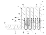
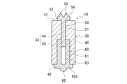
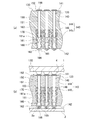
- FIG. 4 is an enlarged cross-sectional view of a portion A of FIG. 3 in the IC socket according to the first embodiment.
- FIG. 7 is an enlarged cross-sectional view showing a state before pressing of the IC socket according to the first embodiment. It is an expanded sectional view showing the state after pressing of IC socket concerning the embodiment 1.
- FIG. 6 is a perspective view showing a first contactor of the IC socket according to the first embodiment.
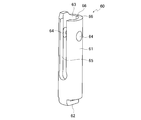
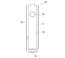
- FIG. 10 is a perspective view showing a second contactor of the IC socket according to the first embodiment.
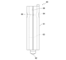
- FIG. 6 is a right side view showing a second contactor of the IC socket according to the first embodiment.
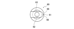
- FIG. 7 is a left side view showing a second contactor of the IC socket according to the first embodiment.
- FIG. 12 is a cross-sectional view of the second contact of the IC socket according to the first embodiment taken along the line BB in FIG. 11; It is a bottom view which shows the 2nd contactor of IC socket concerning the embodiment 1.
- FIG. FIG. 18 is an enlarged cross-sectional view showing a first modified example of the IC socket according to the first embodiment.
- FIG. 21 is an enlarged cross sectional view showing a second modified example of the IC socket in the first embodiment.
- FIG. 21 is a right side view showing a modified example of the second contactor of the IC socket according to the first embodiment. It is a bottom view which shows the modification of the 2nd contact of the IC socket concerning the embodiment 1.
- FIG. 21 is a development view of a modification of the second contactor of the IC socket according to the first embodiment. It is a figure in the middle of bending of the modification of the 2nd contact child of IC socket concerning the embodiment 1.
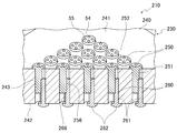
- FIG. FIG. 6 is an enlarged cross-sectional perspective view showing an IC socket according to Embodiment 2 of the present invention.
- FIG. 14 is an enlarged cross-sectional perspective view showing a state in which a part of the first contactor and a part of the second contactor are removed from the sheet member of the IC socket according to the second embodiment.
- FIG. 14 is an enlarged cross-sectional view schematically showing a state before pressing of the IC socket according to the second embodiment.
- FIG. 13 is an enlarged cross-sectional view schematically showing a state after pressing of the IC socket according to the second embodiment.
- FIG. 13 is an enlarged cross-sectional view schematically showing a modification of the IC socket according to the second embodiment. It is a perspective view which shows the IC socket which concerns on Embodiment 3 of this invention.
- FIG. 14 is a front view showing an IC socket according to the third embodiment.
- FIG. 21 is a perspective view showing a second contactor of the IC socket according to the third embodiment.
- FIG. 21 is a front view showing a second contactor of the IC socket according to the third embodiment.
- FIG. 21 is a right side view showing a second contactor of the IC socket according to the third embodiment.
- FIG. 21 is a bottom view showing a second contactor of the IC socket according to the third embodiment.
- FIG. 18 is a development view of a second contactor of the IC socket according to the third embodiment.
- FIG. 7 is an enlarged cross-sectional schematic view showing another example of the IC socket of the present invention.
- FIG. 10 is an enlarged cross-sectional schematic view showing still another example of the IC socket of the present invention. They are the (a) expansion plane schematic diagram and the (b) expansion cross-section schematic diagram which show the further another example of the IC socket of this invention.
- FIG. 37 is an enlarged cross-sectional view schematically showing the state of contact with a solder ball in the IC socket of FIG. 36.
- FIG. 36 (a) shows a state in which the solder ball is uniformly in contact with the first contact; It is a figure of the state which contacted uniformly.
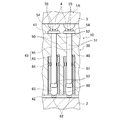
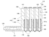
- FIG. 14 is an enlarged cross-sectional view of a portion A of FIG. 3 in the IC socket according to the fourth embodiment.
- (A) is a perspective view showing the first contactor in the IC socket according to the fourth embodiment
- (b) is a perspective view when the second contactor in the IC socket is viewed from the inside
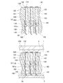
- (c) is the same IC socket It is the perspective view which looked at the 2nd contact child in from the outside. It is the elements on larger scale in IC socket concerning the embodiment 4, (a) shows the state before use, and (b) shows the state in use. It is a partial expanded sectional view in IC socket concerning Embodiment 5 of invention, (a) shows the state before use, (b) shows the state in use.
- (A) is a perspective view which shows the 1st contact in the IC socket concerning Embodiment 6 of the invention
- (b) is a perspective view of the 2nd contact in the same IC socket. It is the elements on larger scale in IC socket concerning Embodiment 6 of the invention, (a) shows the state before use, and (b) shows the state in use.
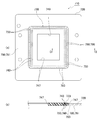
- the IC socket which concerns on Embodiment 7 of invention is shown, (a) is a top view, (b) is sectional drawing, (c) is a partial expanded sectional view.
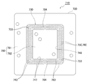
- the IC socket which concerns on the modification of Embodiment 7 of invention is shown, (a) is a top view, (b) is sectional drawing.
- the IC socket which concerns on the other modification of Embodiment 7 of invention is shown, (a) is a top view, (b) is DD sectional drawing of (a).
- the IC socket which concerns on Embodiment 8 of this invention is shown, (a) is a top view, (b) is sectional drawing.
- the IC socket which concerns on Embodiment 9 of this invention is shown, (a) is a top view, (b) is sectional drawing.
- the IC socket 10 as the “electric component socket” of this embodiment is disposed on the wiring board 2 as the “second electric component” as shown in FIGS.
- IC package 1 as a component is accommodated, and it is configured to contact solder ball 4 as a "terminal" of IC package 1 and an electrode (not shown) of wiring substrate 2 to electrically connect the two. There is. Then, this IC socket 10 is used, for example, as a test device of a continuity test such as a burn-in test on the IC package 1 or the like.
- a plurality of spherical solder balls 4 are provided in a matrix in a predetermined range of a substantially square of the lower surface of the substantially square package body 3 (see FIGS. 5 and 6). ).
- the IC socket 10 is disposed on the frame-shaped plate-like frame member 20 disposed on the wiring substrate 2 and at the central portion of the frame member 20 and connected to the frame member 20. And the socket body 30.
- the socket body 30 is configured to be connected to the frame member 20 by four connection portions 31 extending laterally from the lower surface side, as shown in FIGS. 2 to 4. Further, the socket body 30 is configured to accommodate the IC package 1, and a sheet member 40 constituting the whole of the socket body 30 and a plurality of substantially disposed on the sheet member 40 from the upper surface 41 side.
- the first contactor 50 is inserted into the corresponding second contactor 60 in the sheet member 40 to be in contact with and slide in the corresponding contactor.
- the solder balls 4 and the wiring of the IC package 1 are made
- the electrodes of the substrate 2 are configured to be electrically connected via the first contact 50 and the second contact 60.
- the sheet member 40 has a substantially square shape in a plan view, and is made of an insulator having an elastic force. Moreover, in this embodiment, the sheet member 40 is made of, for example, a resin such as silicone rubber or fluororubber as an insulator having elasticity and having durability against a burn-in test heated to 150 ° C. doing.
- a resin such as silicone rubber or fluororubber as an insulator having elasticity and having durability against a burn-in test heated to 150 ° C. doing.
- the sheet member 40 is provided with a through hole 43 penetrating from the upper surface 41 to the lower surface 42.
- a first through hole 44 of such a diameter that the first contact 50 described later can be inserted just enough to slide.
- a second through hole 45 having a diameter (larger than the first through hole 44) to which a second contact 60 described later can be inserted is provided. That is, the through hole 43 has a first through hole 44 provided from the upper surface 41 and a second through hole 45 provided below the first through hole 44 and communicating with the lower surface 42 and having a diameter larger than the first through hole 44. It has a tiered configuration.
- the first contactor 50 is a substantially cylindrical metal member, and is provided at a substantially cylindrical first insertion portion 51 and one end thereof to have a diameter larger than that of the first insertion portion 51.
- the formed first plate-like contact portion 52 (in this case, a substantially disk-like shape).
- a wide portion 53 in which the first insertion portion 51 bulges outward is provided at the other end opposite to the first contact portion 52 of the first insertion portion 51.
- a projection 55 having a predetermined shape is formed on the upper surface 54 of the first contact portion 52.
- the plurality of substantially conical projections 55 are arranged to be spaced apart from each other by a plane shape of the upper surface 54. The projection 55 is in contact with the solder ball 4 of the IC socket 2.
- the second contactor 60 is a substantially cylindrical metal member, and the plate-like member is bent and bent so that the end portions 66 come into contact with each other. And a member formed in a substantially cylindrical shape.
- the cylindrical portion 61 of the second contact 60 is formed in such a size and shape that the hollow portion 63 formed therein can slide in contact with the first insertion portion 51 of the first contact 50. There is.
- a second contact portion 62 for contacting an electrode of the wiring board 2 is provided at an end of the second contactor 60 on the lower surface 42 side of the sheet member 40.
- the second contact portion 62 in this embodiment is formed by bending an end portion of the cylindrical portion 61, and is configured to have a predetermined elastic force.
- a protrusion 64 which protrudes to the inside of the hollow portion 63 is provided so that the diameter of the hollow portion 63 at the position becomes slightly smaller by this protrusion 64. It is formed. Specifically, the diameter of the hollow portion at the position is formed to be narrower than the widened portion 53 of the first insertion portion 51 of the first contactor 50 by the projection 64, and the first insertion portion 51 is formed.
- the first contactor 50 and the second contactor 60 can be easily made by inserting into the hollow portion 63 and pushing the widening portion 53 strongly against the projection 64 so as to be positioned below the projection 64. It is something that can be prevented from coming off.
- a slit 65 is formed on the side surface of the cylindrical portion 61 according to this embodiment from the top to the lower surface side, and the diameter of the hollow portion 63 can be finely changed by the slit 65.
- the hollow portion 63 is expanded by the presence of the slit 65 and the projection 64 is expanded, so that the widening portion 53 can get over the projection 64 and then return to the original diameter. As a result, it becomes difficult for the first contactor 50 and the second contactor 60 to come off easily.
- the first insertion portion 51 of the first contactor 50 is inserted into each first through hole 44 formed in the upper surface 41 of the sheet member 40, and each second penetration formed in the opposite lower surface 42 of the sheet member 40
- the cylindrical portion 61 of the second contact 60 is inserted into the hole 45, and the first insertion portion 51 is slidably inserted into the hollow portion 63 of the cylindrical portion 61, and the widened portion 53 passes over the projection 64 A state in which the first contactor 50 and the second contactor 60 are engaged and the first contact portion 52 is exposed from the upper surface 41 of the sheet member 40 (here, the lower surface of the large diameter first contact portion 52 is the sheet member 40 And the upper end of the cylindrical portion 61 abuts against the step between the first through hole 44 and the second through hole 45, and the second contact portion 62 is exposed from the lower surface 42 of the sheet member 40.
- the second contact portion 62 is the lower surface 42 of the sheet member 40 By the projecting state), and it can accommodate state IC package 1 is disposed on the
- the IC socket 10 is disposed such that the second contact portion 62 of the second contact 60 comes in contact with the terminal of the wiring board 2.
- the IC package 1 is accommodated on the upper surface 41 of the sheet member 40 of the IC socket 10 so that the solder ball 4 of the IC package 1 contacts the first contact portion 52 of the first contact 50.
- the first contact portion 52 is pressed downward by the solder ball 4 of the IC package 1 from the state of FIG.
- the sheet member 40 having an elastic force is pressed on the lower surface, and as shown in FIG. 6, the sheet member 40 is compressed and deformed into a state of having a repulsive force which tends to return to the original state.
- the second contact Press 60 downward.
- a predetermined contact pressure between the first contact portion 52 and the solder ball 4 of the IC package 1 is secured by the upward repulsive force of the sheet member 40, and the second contactor 60 by the end of the first through hole 44.
- the predetermined contact pressure between the second contact portion 62 and the electrode of the wiring board 2 is secured by pressing the cylindrical portion 61 downward.
- the first contactor 50 and the second contactor 60 are connected by the first insertion portion 51 and the hollow portion 63 contacting and sliding. Thereafter, a continuity test such as a burn-in test is performed. The description of the removal of the IC package 1 and the wiring board 2 from the IC socket 10 after the test will be omitted.
- the first contact portion 52 may be bonded with a bonding agent S (the entire first insertion portion 51 is not bonded) from a position where the first contact portion 52 is in contact with a predetermined amount of lower portion. If comprised in this way, the sheet
- the second contact portion 62 of the second contactor 60 may have a large diameter portion 62a in a bowl shape. With this configuration, the second contact portion 62 also presses the lower surface 42 of the sheet member 40 in the same manner as the first contact portion 52 presses the upper surface 41 of the sheet member 40. The sheet member 40 can be pressed by pressing from the side, and the sheet member 40 can be compressed and deformed more easily.
- the shape of the second contactor 60 may be a shape different from the above-described shape, as in the case of the second contactor 160 shown in FIG. 16 to FIG.
- the second contact 160 is configured to form each half of the cylindrical portion 161 about the second contact portion 162 in the developed view. Then, as shown in FIG. 20, while bending each half of the cylindrical portion 161, the second contact portion 162 is bent so as to protrude substantially at the center, so that the shape as shown in FIGS.
- the second contact 160 is formed. Also in this shape, the same function and effect as those of the second contactor 60 described above can be obtained.
- the first contactor 50 and the second contactor 60 are provided from the mutually facing surfaces 41 and 42 of the sheet member 40 made of an insulator having elastic force.
- the sheet member 40 is deformed by pressing the first contactor 50 and the second contactor 60 between the IC package 1 and the wiring substrate 2 because they are inserted to be in contact with each other, and the elastic force is used to make an IC.
- the package 1 and the wiring substrate 2 can be electrically connected with a predetermined contact pressure. As a result, it becomes unnecessary to separately provide a biasing member such as a coil spring, which is conventionally required, and the number of parts can be reduced to reduce the cost of the IC socket 10.
- the first contactor 50 has the plate-like first contact portion 52, and the first contact portion 52 contacts the first surface 41. Since the sheet member 40 is deformed by the first contact portion 52 by being pressed by the IC package 1, the sheet member 40 can be reliably pressed and deformed to exert an elastic force.
- the first insertion portion 51 of the first contact 50 slides in a state of being inserted into and in contact with the inside of the cylindrical portion 61 of the second contact 60
- the first contact portion 52 of the first contactor 50 and the second contact portion 62 of the second contactor 60 can be arranged substantially coaxially, and as a result, the IC package 1 and the wiring substrate The two can be disposed at substantially the same positions facing each other without shifting.
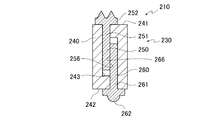
- Second Embodiment of the Invention 21 to 24 show a second embodiment of the present invention.
- the embodiment of the present invention is the same as that of the first embodiment described above except for the matters described below, and therefore, the explanation will be omitted except for the matters different from the first embodiment described above.
- both the first contact 250 and the second contact 260 are both formed of substantially rod-like members, and the first contact 250 is formed at the one end of the substantially rod-shaped first insertion portion 251 and the first contact 251.
- the first contact portion 252 has a diameter larger than that of the first insertion portion 251
- the second contactor 260 is formed at the one end of the substantially rod-like second insertion portion 261 having a diameter smaller than the first insertion portion 251.
- the second contact portion 262 has a diameter larger than that of the second insertion portion 261.
- the widening portion 53 formed at the other end of the first insertion portion 51 of the first contactor 50 of the first embodiment described above corresponds to the first contactor 250 and the second contactor 260 of this embodiment. Has not been formed.
- the through hole 243 of the sheet member 240 has a shape in which the large hole portion 244 and the small hole portion 245 are connected side by side and in communication.
- the first insertion portion 251 of the first contactor 250 is inserted into the large hole portion 244 of the through hole 243 from the upper surface 241 side, and the second insertion portion 261 of the second contactor 260 is inserted into the small hole portion 245 of the through hole 243
- the side surfaces 256 and 266 are in contact with each other and slide.
- the first contact portion 252 of the first contact 250 in the state as shown in FIG. 23 is pressed by the solder ball 4 of the IC package 1 from the upper surface 241 side, and the second contact of the second contact 260
- the sheet member 240 is pressed, and accordingly, the first insertion portion 251 and the second insertion portion 261 are in contact. It slides in the state and is compressed and deformed.
- the 1st insertion part 251 of the 1st contactor 250 and the 2nd contactor 260 2nd insertion part 261 of this embodiment were formed in the substantially cylindrical shape, it does not restrict to this, For example, It may be formed in other shapes, such as a prismatic shape such as a prismatic prism and a triangular prism, and a semi-cylindrical shape. It is preferable that the shape is such that the area is increased, such as the contact sliding position of the first contactor 250 and the second contactor 260 being in a planar shape, in particular, because the electrical connection can be performed better.
- the sheet T1 (having a predetermined hardness and thickness) on the lower surface of the first contact portion 252 of the first contact 250 (on the upper surface 241 of the sheet member 240).
- An insulating sheet having rigidity higher than that of the sheet member 240 is preferable), and a sheet having a predetermined hardness and thickness on the upper surface (below the lower surface 242 of the sheet member 240) of the second contact portion 262 of the second contactor 260 T2 (insulation sheet having higher rigidity than the sheet member 240 is preferable) may be provided.
- the load of the pressing force of the sheet member 240 by the first contact portion 252 and the load of the pressing force of the sheet member 240 by the second contact portion 262 can be dispersed, so that the sheet member 240 as a whole is uniform. Can be loaded.
- the first contactor 250 and the second contactor 260 are provided from the facing surfaces 241 and 242 of the sheet member 240 made of an insulator having elastic force.
- the sheet member 240 is deformed by pressing the first contactor 250 and the second contactor 260 between the IC package 1 and the wiring substrate 2 because they are inserted to be in contact with each other, and the elastic force is used to make an IC.
- the package 1 and the wiring substrate 2 can be electrically connected with a predetermined contact pressure. As a result, it becomes unnecessary to separately provide a biasing member such as a coil spring, which is conventionally required, and the number of parts can be reduced to reduce the cost of the IC socket 210.
- the first contactor 250 has the plate-like first contact portion 252, and the first contact portion 252 contacts the first surface 241. Since the sheet member 240 is deformed by the first contact portion 252 by being pressed by the IC package 1, the sheet member 240 can be reliably pressed and deformed to exert an elastic force.
- the first insertion portion 251 of the first contact 250 and the second insertion portion 261 of the second contact 260 are both formed in a substantially rod shape, and the side surfaces of each other
- the first contact 250 and the second contact 260 can be made simpler because they are configured to slide in a state in which the two contacts 256 and 266 are in contact with each other.
- the IC socket 210 can be manufactured. The cost can be further reduced.
- Third Embodiment of the Invention 26 to 33 show a third embodiment of the present invention.
- the embodiment of the present invention is the same as that of the first embodiment described above except for the matters described below, and therefore, the explanation will be omitted except for the matters different from the first embodiment described above.
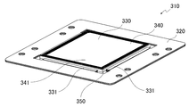
- the IC socket 310 is, as shown in FIGS. 26 to 28, a frame-shaped plate-like frame member 320 disposed on the wiring substrate 2 and a central portion of the frame member 320 disposed and connected to the frame member 320. And a socket body 330.
- the socket body 330 has four connecting portions 331 extending laterally from the lower surface side of a first sheet member 340a to be described later and the upper surface side of a second sheet member 340b. Configured to be connected to Also, the socket body 330 is configured to accommodate the IC package 1, and a sheet member 340 constituting the whole of the socket body 330, and a plurality of substantially disposed on the sheet member 340 from the upper surface 341 side.
- the first contactor 350 is inserted into the corresponding second contactor 360 in the sheet member 340 to be in contact with and slide on the corresponding second contactor 360.
- the solder balls 4 of the IC package 1 and the wiring The electrodes of the substrate 2 are electrically connected via the first contact 350 and the second contact 360.
- the sheet member 340 has a substantially square shape in plan view, and two sheet members of the first sheet member 340a and the second sheet member 340b having an elastic force overlap each other. Is configured.
- the first sheet member 340a is provided with a first through hole 344 having a diameter which can be inserted so that a first contact 350 described later just slides so as to penetrate downward from the upper surface 341 .
- the second sheet member 340 b has a diameter (larger than the first through hole 344) that can be inserted so that a second contact 360 described later just slides so as to penetrate upward from the lower surface 342.
- Two through holes 345 are provided.
- the first through hole 344 provided from the upper surface 341 and the lower side thereof are in communication with the lower surface 342 and larger in diameter than the first through hole 344 It has a two-stage configuration having a second through hole 345.
- the first sheet member 340a and the second sheet member 340b may be configured to be made of different materials. For example, if the first sheet member 340a is harder than the second sheet member 340b, the sheet member 340 has a greater repulsive force when it is compressed and deformed. The contact pressure to the wiring board 2 can be increased.
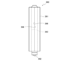
- the second contactor 360 is a substantially cylindrical metal member, and the plate-like member is bent and bent so that the end portions 366 and 366 are in contact with each other. It is a member which is made to have a substantially cylindrical shape.
- the cylindrical portion 361 of the second contact 360 is formed in such a size and shape as to allow the hollow portion 363 formed therein to slide in contact with the first contact portion 352 of the first contact 350. There is.
- a second contact portion 362 for contacting an electrode of the wiring substrate 2 is provided at an end of the second contactor 360 on the lower surface 342 side of the sheet member 340.
- the second contact portion 362 in this embodiment is formed by bending an end portion of the cylindrical portion 361, and is configured to have a predetermined elastic force.
- the first insertion portion 351 of the first contact 350 is inserted into each first through hole 344 formed in the upper surface 341 of the sheet member 340, and each second penetration formed in the opposed lower surface 342 of the sheet member 340.
- the cylindrical portion 361 of the second contact 360 is inserted into the hole 345, and the first insertion portion 351 is slidably inserted into the hollow portion 363 of the cylindrical portion 361, so that the first contact 350 and the second contact And the first contact portion 352 is exposed from the upper surface 341 of the sheet member 340 (here, the lower surface of the large diameter first contact portion 352 is in contact with the upper surface 341 of the sheet member 340).
- the entire side surface of the cylindrical portion 361 of the second contact 360 and the second sheet member 340 b are bonded with an adhesive to form a first contact.
- the first sheet member 340a is adhered with an adhesive to a predetermined amount downward from the position where the lower surface of the first contact portion 352 of the child 350 and the first contact portion 352 of the first insertion portion 351 contact (the first insertion portion 351 The whole may not be adhered). With such a configuration, the sheet member 340, the first contact 350, and the second contact 360 can be held in a stable state.
- the first contactor 350 and the second contactor 360 are provided from the mutually facing surfaces 341 and 342 of the sheet member 340 made of an insulator having elastic force.
- the sheet member 340 is deformed by pressing the first contactor 350 and the second contactor 360 between the IC package 1 and the wiring substrate 2 because they are inserted so as to be in contact with each other.
- the package 1 and the wiring substrate 2 can be electrically connected with a predetermined contact pressure. As a result, it becomes unnecessary to separately provide a biasing member such as a coil spring, which is conventionally required, and the number of parts can be reduced to reduce the cost of the IC socket 310.
- the first contact 350 has the plate-like first contact portion 352, and the first contact portion 352 contacts the first surface 341. Since the sheet member 340 is deformed by the first contact portion 352 by being pressed by the IC package 1, the sheet member 340 can be reliably pressed and deformed to exert an elastic force.
- the sheet member 340 is constituted by two members of the first sheet member 340a and the second sheet member 340b, and the second sheet member 340b of the first sheet member 340a. Since the end of the second sheet member 340b is pressed at the end on the side facing the first sheet member 340a, the first sheet member is deformed when the sheet member 340 is deformed. As a result, the IC package 1 and the wiring substrate 2 can be electrically connected with a more reliable contact pressure by the elastic force of the first sheet member 340a. .
- the “electric component socket” of the present invention is not limited to the structure as in each of the first to third embodiments described above, and may be applied to other structures such as devices other than IC sockets. .
- the “electric component socket” of the present invention is not limited to the configuration of each of the first to third embodiments described above, and may be another configuration.
- the IC socket 410 has a configuration in which the conductive filler 460 as the second contactor is solidified with the resin 446 in the through hole 443 provided in the sheet member 440.
- the first insertion portion 451 of the first contactor 450 is inserted from the upper surface 441 side in the inside of the 446, and the first contact portion 452 of the first contactor 450 is exposed, and the first insertion portion 451 and the conductive filler
- the first contact portion 452 and the second contact portion 462 electrically connected to the first contact portion 452 and the second contact portion 462 exposed to the conductive filler 460 on the lower surface 442 side are electrically connected to the first electric component 1 and the second electric component 2. It may be a
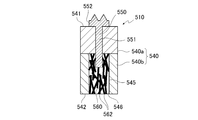
- the IC socket 510 has a configuration in which the conductive filler 560 as the second contactor is solidified with the resin 546 in the first sheet member 540 a having the first through hole 544 and the second through hole 545. And the first insertion portion 551 of the first contactor 550 is inserted from the upper surface 541 side of the sheet member 540, and the first contactor 550 of the first contactor 550. The first contact portion 552 is exposed, and the first insertion portion 551 and the conductive filler 560 in the second sheet member 540b are electrically connected, and the first contact portion 552 and the conductive filler 560 are on the lower surface 542 side. It may be made to contact the 1st electric component 1 and the 2nd electric component 2 by the 2nd contact part 562 exposed to.
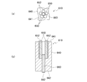
- the IC socket 610 has a rod-like second contact 660 inserted from the lower surface 642 side of the sheet member 640 and a plurality of the IC sockets 610 inserted from the upper surface 641 side of the sheet member 640.
- first contactor 650 It has a rod-like first contactor 650, and these contact and slide in the sheet member 640, and from the upper surface 641 side of the sheet member 640, the tips of the plurality of first contactors 650
- the first contact portion 652 is exposed and contacts the terminal 4 of the first electric component 1 at multiple points
- the second contact portion 662 at the tip of the second contact 660 is exposed from the lower surface 642 side of the sheet member 640
- the first contact portion 652 and the second contact portion 662 may be brought into contact with the first electrical component 1 and the second electrical component 2 by contacting the electrode of the electrical component 2 .
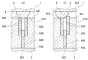
- Such a configuration of the IC socket 610 allows the plurality of first contacts 650 to move independently. Therefore, as shown in FIG. 37 (a), when the terminals 4 of the first electric component 1 contact the plurality of first contacts 650 of the IC socket 610 equally, the plurality of first contacts 650 can be obtained. Moves up and down in a uniform state to contact the terminal 4 at multiple points. On the other hand, as shown in FIG. 37 (b), when the terminals 4 of the first electrical component 1 are in an uneven and shifted state with respect to the plurality of first contacts 650 of the IC socket 610.
- Some of the first contacts 650 are pushed in more greatly, and the pressing of the other first contacts 650 is moved up and down in a non-uniform state where it is small, and in such a state the multipoint contact to the terminal 4 Do. As a result, even if the terminal 4 of the first electrical component 1 is displaced, multipoint contact can be made by the plurality of first contactors 650, and electrical connection can be maintained.
- the shape of the projection of the first contact portion of the first contact is not limited to the above-described shape, and may be any suitable shape such as a so-called crown shape or a cone shape as a whole. Also good.
- Fourth Embodiment of the Invention 38 to 40 show a fourth embodiment of the present invention.
- the IC socket 110 as the “electric component socket” of this embodiment is disposed on the wiring board 2 as the “second electric component” as in the first embodiment of the invention, and the “first electricity” is formed on the top surface.
- the IC package 1 as the component is accommodated, and the solder ball 4 as the “terminal” of the IC package 1 is electrically connected to the electrode 2 a of the wiring substrate 2.
- the IC socket 110 is used, for example, as a testing device of a continuity test such as a burn-in test on the IC package 1.
- a plurality of spherical solder balls 4 are provided in a matrix in a predetermined range of a substantially square of the lower surface of the substantially square package body 3.
- the IC socket 110 has a frame member 120 disposed on the wiring substrate 2 and a socket main body 130 disposed at a central portion of the frame member 120 and connected to the frame member 120.
- the socket body 130 is configured to be connected to the frame member 120 by four connection portions 131 extending laterally from the lower surface side. Also, the socket body 130 is configured to accommodate the IC package 1, and a sheet member 140 that constitutes the whole of the socket body 130, and a large number of contact pins 133 arranged in a matrix on the sheet member 140. And have.
- Each contact pin 133 is inserted into the sheet member 140 from the plurality of substantially rod-shaped first contactors 150 inserted into the through hole 143 from the upper surface 141 side, and inserted into the sheet member 140 from the lower surface 142 into the through hole 143 And a substantially half-pipe-shaped second contactor 160.
- the first contactor 150 is slidable in contact with the second contactor 160 disposed laterally on the inside of the through hole 143 of the sheet member 140, and the solder ball of the IC package 1 is 4 and the electrodes of the wiring board 2 are configured to be electrically connected via the first contact 150 and the second contact 160.
- the sheet member 140 has a substantially square shape in plan view.
- the sheet member 140 is made of an elastic body having elasticity and is made of an insulator having durability against a burn-in test heated to 150 ° C., for example, a resin such as silicone rubber or fluorine rubber.
- the sheet member 140 is provided with a through hole 143 penetrating between the upper surface 141 and the lower surface 142.
- a first through hole 144 having a diameter to which the first contact 150 can be slidably inserted is provided.
- the second contactor 160 can be inserted up to the middle, and a second through hole 145 larger in diameter than the first through hole 144 is provided.
- the first through hole 144 on the upper surface 141 side and the second through hole 145 on the lower surface 142 have coaxial steps in the inner wall with a step 146 and have a two-stage configuration.
- the first contact 150 is a substantially cylindrical metal member, and is provided at a substantially cylindrical first insertion portion 151 and one end of the first insertion portion 151.
- the first contact portion 152 is formed larger than the first through hole 144 and has a substantially disc shape, and can be in contact with the upper surface 141 around the through hole 143.
- a plurality of substantially conical projections 155 are provided on the upper surface 54 of the first contact portion 152 at an interval from each other via the planar shape of the upper surface 54.
- the plurality of projections 155 are in contact with the solder balls 4 of the IC package 1.
- the opposing portion of the first contact portion 152 with the sheet member 140 elastically deforms by pressing the sheet member 140 by the first contact portion 152 when a force in a direction along the through hole 143 acts on the first contact 150. It is configured to
- the end of the first insertion portion 151 opposite to the first contact portion 152 extends along the through hole 143, and is provided with a rod-like first insertion portion 151 disposed to the side of the second contact 160. It is done.
- the first insertion portion 151 is slidable in the direction along the through hole 143 in contact with the inner wall of the through hole 143.
- the second contact 160 is a metal member formed in a substantially half pipe shape as shown in FIGS. 39 (b) and (c), and is inserted into the through hole 143 to be a side of the first contact 150 And a second contact portion 162 provided at one end thereof and in contact with the wiring board 2.
- the second insertion portion 161 has a second insertion portion main body 161 a having a cross-sectional shape in the direction intersecting with the through hole 143 having an arc piece shape and extending smoothly and continuously along the through hole 143; And a projecting portion 170 which is made to project in a direction intersecting with the through hole 143.
- the shape of the projecting portion 170 can be set appropriately, but in the present embodiment, the second contact portion 162 side is continuous from the second insertion portion main body 161 a at the upper end side at the middle position in the longitudinal direction of the second insertion portion main body 161 a. It is formed in the shape which protruded inside the arc-like 2nd insertion part main body 161a.
- a second contact portion 163 is provided which abuts the step 146 of the through hole 143 in the direction along the through hole 143.
- the second contact portion 163 is configured to be in contact with and supported by the step 146 when a force in a direction along the through hole 143 acts on the second contact 160.
- the second contact portion 162 for contacting the electrode 2a of the wiring board 2 is narrower than the second insertion portion 161 and the second insertion portion It is formed in the shape bent from 161.
- each of the plurality of through holes 143 provided in a matrix shape is formed to penetrate between the upper surface 141 and the lower surface 142 of the sheet member 140.
- the first contactor 150 and the second contactor 160 are used by being inserted and arranged.
- each second contact 160 inserts the arc-shaped second insertion portion 161 into each through hole 143 from the lower surface 142 side of the sheet member 140, and the second contact portion 163 is a step in the through hole 143.
- the second contact portion 162 is disposed in a state where the second contact portion 162 protrudes from the lower surface 142 side while being in contact with the surface 146.
- each first contactor 150 inserts the rod-shaped first insertion portion 151 into the through hole 143 from the upper surface 141 side of the sheet member 140, and further to the inside of the arc-shaped second insertion portion main body 161a.
- the first insertion portion 151 and the second insertion portion 161 are adjacent to each other in the direction intersecting with the through hole 143, and the first contact portion 152 is brought into contact with the upper surface 141 of the sheet member 140.
- the rod-shaped first insertion portion 151 of the first contact portion 152 When the first insertion portion 151 of the first contact 150 is inserted inside the arc-shaped second insertion portion main body 161 a of the second contact 160, the rod-shaped first insertion portion 151 of the first contact portion 152 The first insertion portion 151 of the first contactor 150 and the projection portion 170 of the second contactor 160 are adjacent to the protrusion 170 provided in the second insertion portion 161 in a direction crossing the through hole 143. It is arranged in contact.
- the first insertion portion 151 of the first contactor 150 and the second insertion portion main body 161a of the second contactor 160 respectively abut the inner wall of the through hole 143, and the inner wall of the through hole 143 in the radial direction It arranges in the state where it pressed.
- the elastic force of the sheet member 140 is applied to the first insertion portion 151 and the second insertion portion 161 in the direction intersecting with the through hole 143, and the first insertion portion 151 of the first contactor 150 and the second insertion portion 161
- the elastic force of the sheet member 140 makes pressure contact with the protrusion 170 of the contact 160.
- the IC socket 110 is disposed on the wiring board 2 and the lower surface 142 of the sheet member 140 is disposed at a predetermined position on the wiring board 2.
- the second contact portion 162 of the second contact 160 is brought into contact with and fixed to the electrode 2 a of the wiring board 2. In this state, it is used as a test apparatus such as a burn-in test.
- the IC package 1 is disposed on the upper side of the socket 1 and placed on a predetermined position of the upper surface 141 of the socket body 130. Further, by pressing the IC package 1 downward, the solder balls 4 of the IC package 1 are brought into pressure contact with the first contact portion 152 of the first contact 150.
- the first insertion portion 151 of the first contact 150 and the second introduction portion 61 of the second contact 160 are in the through holes 143. Since it is inserted and pressed in a direction crossing the through hole 143 by the elastic force of the sheet member 140, the projection of the first insertion portion 151 is caused even if the first contactor 150 is pushed down by the solder ball 4 The portion 170 and the second insertion portion 161 are maintained in a pressure-contacted state. Even when the first contactor 150 is lowered to the lowermost position as shown in FIG. 40 (b), the elastic force of the sheet member 140 causes the protruding portion 170 of the first insertion portion 151 to be in pressure contact with the second insertion portion 161. There is.
- the first contact portion 152 presses the position corresponding to each first contact portion 152 on the upper surface 141 of the sheet member 140 and elastically deforms, whereby the elastic force of the sheet member 140 is generated. A reaction force is obtained, and the first contact portion 152 and the solder ball 4 can be brought into pressure contact with a sufficient contact pressure.
- each electrode 2a of the wiring board 2 and each solder ball 4 of the IC package 1 are reliably connected via the second contactor 160 and the first contactor 150, and are energized and used as a test apparatus. Can.
- the sheet member 140 made of an insulator having elastic force has the through hole 143 and the first contactor 150 contacting the IC package 1 and the wiring substrate 2
- the second contact 160 to be in contact is inserted into the through hole 143, and the protrusion 170 provided on the first contact 150 is in pressure contact with the second contact 160 by the elastic force of the sheet member 140. Therefore, the first contactor 150 and the second contactor 160 can be reliably brought into contact in the through hole 143.
- the first contact portion 150 has the first contact portion 152 in contact with the upper surface 141, and the first contact portion 152 is pressed by the IC package 1 so that the sheet member 140 is the first.
- the first contact portion 152 can be brought into contact with the IC package 1 with sufficient contact pressure by the reaction force of the sheet member 140 because the contact portion 152 is pressed and elastically deformed. There is no need to provide it separately, and the structure can be simplified.
- the second contact 160 since the second contact 160 has the second contact portion 163 that contacts the step 146 provided in the through hole 143, the reaction force at the step 146 of the sheet member 140 is obtained.
- the second contact portion can be stably brought into pressure contact with the electrode 2 a of the wiring substrate 2.
- a second contact portion 160 extends along the through hole 143 and has a second insertion portion 161 having an arc piece shape in cross section intersecting the through hole 143.
- Has a rod-shaped first insertion portion 151 which extends along the through hole 143 and is inserted inside the arc-shaped second insertion portion 161, the first contact 150 is formed in the through hole 143.
- the 1st insertion part 151 can be arrange
- FIGS. 41 (a) and 41 (b) are partially enlarged cross-sectional views of the IC socket according to the fifth embodiment of the present invention.
- the IC socket 110 of the fifth embodiment is the same as the fourth embodiment except that the structure of the contact pin 133 is different.
- the first insertion portion 151 of the first contact 150 is provided with the projecting portion 170, and the second insertion portion 161 of the second contact 160 is provided.
- the protrusion 170 is not provided.
- the protruding portion 170 of the first insertion portion 151 is formed in a fine lump on the tip end side of the rod-shaped first insertion portion 151 so as to protrude in the direction intersecting the through hole 143.
- the entire second insertion portion 161 of the second contact 160 follows the through hole 143 in a cross-sectional shape of a circular arc piece in a direction intersecting the through hole 143 like the second insertion portion main body 161 a of the first embodiment. It is provided smoothly and continuously in the direction.
- the socket main body 130 is configured in a state in which the first contact 150 and the second contact 160 are inserted into the through hole 143 of the sheet member 140, and the first insertion of the first contact 150 is performed.
- the projecting portion 170 of the portion 151 and the second insertion portion 161 of the second contact 160 are in pressure contact with each other by the elastic force of the sheet member 140 from the wall portion of the through hole 143.
- the sheet member 140 of the socket body 130 is disposed at a predetermined position of the wiring substrate 2 and the IC chip 10 is placed on the upper side of the socket body 130. Place and press.
- the contact 52 of the first contact 150 and the second contact is in pressure contact with the electrode 2 a of the wiring substrate 2 and the solder ball 4 of the IC package 1.
- Sixth Embodiment of the Invention 42 and 43 are partially enlarged cross-sectional views of the IC socket 110 according to the sixth embodiment of the present invention.
- This IC socket 110 has the same configuration as that of the fourth embodiment of the invention except that the configuration of the second contactor 160 is different.
- the first contacts 150 are the same as those of the fourth embodiment of the invention as shown in FIG. 42 (a), and the second contacts 160 are mutually as shown in FIG. 42 (b).
- a pair of second insertion portions 161 extending along the through holes 143 so as to face each other, and a second connecting portion 165 connecting the second insertion portions 161 at one end of each of the second insertion portions 161 There is.
- the pair of second insertion portions 161 are configured in the same manner as the second insertion portions 161 of the second contactor 160 in the fourth embodiment, and the cross-sectional shape in the direction intersecting with the through hole 143 is substantially arc-shaped It is formed.
- the cross-sectional shape of the second connection portion 165 in the direction along the through hole 143 is formed by being folded in a substantially U-shape, and is continuous with the second insertion portion 161 at both ends.
- the folded back portion of the second connection portion 165 is a portion which is disposed so as to protrude from the lower surface 142 of the sheet member 140, and the contact convex portion 166 with the electrode 2a of the wiring substrate 2 is provided so as to protrude downward.
- the pair of second insertion portions 161 of the second contact 160 is inserted into the through hole 143 in a state of being folded back by the second connection portion 165.
- the tip end of the second insertion portion 161 is brought into contact with the step 146 of the through hole 143.
- the rod-shaped first insertion portion 151 of the first contact 150 is inserted into the through hole 143 from the upper surface 141 side of the sheet member 140, and the first contact portion 152 is brought into contact with the upper surface 141.
- the first insertion portion 151 is held between the second insertion portions 161.
- the socket body 130 is formed.
- FIG. 43 (b) it is used as a test apparatus as in the fourth embodiment of the invention. That is, the sheet member 140 of the socket body 130 is disposed at a predetermined position of the wiring substrate 2 and the IC chip 10 is pressed from the upper side of the socket body 130.
- the contact 52 of the first contact 150 and the second contact of the second contact 160 And 162 are in pressure contact with the electrodes 2 a of the wiring substrate 2 and the solder balls 4 of the IC package 1.
- the second contacts 160 have a pair of second insertion parts 161 extending along the through holes 143 so as to face each other, and the first insertion parts 151 of the first contacts 150 are Since the second insertion portion 161 is inserted and held between the second insertion portions 161, the first insertion portion 151 of the first contact 150 is more strongly contacted to the second insertion portion 161 of the second contact 160 in the through hole 143. be able to. Therefore, more reliable connection between the first contactor 150 and the second contactor 160 can be realized.
- the protrusion 170 is provided on either the first contact 150 or the second contact 160, but the first insertion portion 151 of the first contact 150 and the second of the second contact 160 are provided. It is also possible to provide a projection 170 that protrudes in the direction intersecting with the through hole 143 in both the insertion portion 161.
- the second insertion portion 161 of the second contact 160 is provided with a notch to form the protrusion 170, and in the fifth embodiment, the first insertion portion of the first contact 150 is formed.
- the protrusions 170 are formed in a fine lump at 151, but the shape and position of the protrusions 170 are determined by the elastic force of the sheet member 140 in the through hole 143 between the first contact 150 and the second contact 160. It is not limited at all as long as it is a shape and a position where the space can be in contact, and can be set as appropriate.
- the shapes of the first insertion portion 151 and the first contact portion 152 of the first contact 150 and the shapes of the second insertion portion 161 and the second contact portion 162 of the second contact 160 are the same as in the fourth to third embodiments.
- the shape is not limited at all, and can be formed into various shapes.
- the protrusion 170 is provided in the second insertion portion 161 of the second contact 160 so that the first contact 150 is in pressure contact.
- 170 may be provided to be in pressure contact with the second insertion portion 161 of the second contact 160, and the projection 170 may be provided at different positions in the longitudinal direction of the first contact 150 and the second contact 160, respectively.
- the first contact 150 and the second contact 160 may be brought into pressure contact with the positions corresponding to the protrusions 170, respectively.
- the entire sheet member 140 from the upper surface 141 to the lower surface 142 is integrally formed of an elastic body, but the sheet member 140 can be configured by overlapping a plurality of sheet materials. It is.
- each of the first through holes 144 is a sheet material in which a large number of first through holes 144 are provided at a predetermined position and a sheet material in which a large number of second through holes 145 are provided in a predetermined position.
- the sheet member 140 may be configured by laminating so that the through holes 143 are configured by axially adjacent communication between the second through holes 145 and the second through holes 145.
- the socket body 130 can be configured even if the elasticity of the other layers is low.
- FIG. 44 shows an IC socket according to Embodiment 7 of the present invention, in which (a) is a plan view, (b) a sectional view, and (c) a partially enlarged sectional view.
- the IC socket 710 as the “electric component socket” of this embodiment is disposed on the wiring board as the “second electric component”, and the “first An IC package as an electrical component is accommodated, and a large number of contact pins 733 are provided to electrically connect solder balls as "terminals" of the IC package to the electrodes of the wiring substrate.
- the IC socket 710 is used, for example, as a testing device of continuity test such as burn-in test for an IC package.
- the IC socket 710 has a frame member 720 disposed on the wiring substrate, and a socket main body 730 disposed at a central portion of the frame member 720 and fixed to the frame member 720.
- the IC socket 710 includes a sheet member 740 on which a large number of contact pins 733 are disposed, and a fixing plate 780 for fixing and supporting the edge 747 of the sheet member 740, and the fixing plate 780 is outside.
- a portion 781 and an inner portion 782 are provided. Therefore, the frame member 720 is constituted by the outer side 781 of the fixing plate 780, and the socket main body 730 is constituted by the sheet member 740 and the inner side 782 of the fixing plate 780.
- Each contact pin 733 includes a first contact 750 and a second contact 760, which are arranged in a large number on the sheet member 740 and disposed at a predetermined position.
- the first insertion portion 751 of the first contact 750 The second insertion portion 761 of the second contactor 760 is pressed against each other by the elastic force of the sheet member 740.
- the sheet member 740 is made of an insulator having elastic force, and is integrally formed with the fixing plate 780.
- the sheet member 740 is made of, for example, a resin such as silicone rubber or fluorine rubber as an insulator having durability against a burn-in test heated to 150 ° C.
- the sheet member 740 is disposed to correspond to the portion of the socket body 730 where the multiple contact pins 733 are disposed, and is formed in a substantially strip shape in a plan view.
- the sheet member 740 having a substantially band shape is formed in a substantially frame shape in a plan view by being continuous with the bent shape.
- the sheet member 740 is formed thicker than the fixing plate 780, and has a thickness capable of stably supporting the first contact 750 and the second contact 760 of each contact pin 733. Specifically, the sheet member 740 has a thickness that can accommodate the first insertion portion 751 and the second insertion portion 761 of the contact pin 733.
- Through holes 743 for disposing the contact pins 733 are provided at predetermined positions in the sheet member 740 at positions where the large number of contact pins 733 are disposed.
- the belt-like sheet members 740 are arranged in an array.
- the first contactor 750 and the second contactor 760 similar to the first to sixth embodiments are disposed in each through hole 743, but detailed illustration is omitted.
- the fixing plate 780 is formed in a plate shape that is harder than the sheet member 740 and thinner than the sheet member 740.
- an outer portion 781 disposed outside the substantially frame-like sheet member 740 and an inner portion 782 disposed inside the sheet member 740 are separately separated from each other. It is provided.
- the shape in plan view of the fixing plate 780 corresponds to the shape of the IC socket 710, the outer side 781 has a shape corresponding to the semiconductor substrate, and the inner side 782 has a shape corresponding to the IC package.
- the sheet member 740 is fixed to the fixing plate 780 at the edge 747, and is fixed to the fixing plate 780 on both sides of the strip-like sheet member 740, preferably over the entire length, particularly preferably around the entire circumference.
- the outer edge 747 of the substantially frame-like sheet member 740 is fixed to the outer side 781 of the fixing plate 780, and the inner edge 747 of the sheet 740 is on the inner side 782 of the fixing plate 780. It is fixed, and the outer side 781 and the inner side 782 of the fixing plate 780 are connected by the sheet member 740.
- the fixing method of the sheet member 740 to the fixing plate 780 is not particularly limited, but a large number of fixing holes 783 penetrating in the thickness direction are provided in a portion of the fixing plate 780 corresponding to the edge 747 of the sheet member 740 At the time of molding of the member 740, resin materials may be molded integrally into the respective fixing holes 783.
- the sheet member 740 since the edge 747 of the sheet member 740 is fixed to the fixing plate 780 harder than the sheet member 740, the sheet member 740 having an elastic force. Edge 747 can be firmly supported non-displaceably.
- the fixing plate 780 Therefore, distortion and deformation of the sheet member 740 can be suppressed by the fixing plate 780, and the positional accuracy of the portion where the first contactor 750 and the second contactor 760 are inserted and arranged in the sheet member 740 can be secured.
- the positional accuracy of the edge 747 of the sheet member 740 is secured by preventing distortion or deformation of the sheet member 740 fixed to the fixing plate 780. It is possible. As a result, it is possible to secure the positional accuracy of the large number of through holes 743 provided in the sheet member 740 and arrange the first contactor 750 and the second contactor 760 with high accuracy.
- the sheet member 740 is formed in a band shape having a thickness capable of accommodating the first insertion portion and the second insertion portion, and both sides of the sheet member 740 are fixed to the fixing plate 780. Since it is fixed, both sides of the strip-like sheet member 740 can be firmly supported non-displaceably, and when the sheet member 740 shrinks, tension acts evenly from both sides.
- the sheet member 740 can be prevented from being distorted to one side, and the positional accuracy of the first contactor 750 and the second contactor 760 stably disposed on the sheet member 740 can be improved.
- the belt-like sheet member 740 in which the plurality of first and second contacts 750 and 760 are disposed substantially all over is formed in a substantially frame shape, and the fixing plate 780 is a sheet. It has an outer portion 781 disposed outside the member 740 and an inner portion 782 disposed inside.
- the outer edge 781 and the inner edge 782 of the fixing plate 780 can firmly support the inner edge 747 and the outer edge 747 of the substantially frame-like sheet member 740 in a non-displaceable manner.
- tension acts in a balanced manner from both the inside and outside.
- the substantially frame shaped sheet member 740 can be prevented from contracting and distorting to one side of the outer side and the inner side, and the arrangement site of the first contact 750 and the second contact 760 in the substantially frame shaped sheet member 740 Position accuracy can be improved.
- the outer side portion 781 and the inner side portion 782 of the fixing plate 780 are separated from each other, and therefore, they are disposed between the outer side portion 781 and the inner side portion 782
- the tension of the sheet member 740 can be evenly distributed over the substantially frame shape. Therefore, the tension acting on the plurality of first contacts 750 and the second contacts 760 in the sheet member 740 can be equalized to facilitate securing the position accuracy.
- the sheet member 740 since the sheet member 740 has the inner opening 749 and the fixing plate 780 is disposed in the inner opening 749, the sheet member 740 is disposed on the inner side of the sheet member 740. There is not a large amount of the elastic material to be configured, and tension due to contraction or the like when forming the elastic material does not act. Moreover, even if the sheet member 740 is provided with the inner opening 749, the fixing plate 780 can firmly support the inner edge 747 in a non-displaceable manner. Therefore, the sheet member 740 can be reliably prevented from contracting and distorting inward, and the positional accuracy of the arrangement portion of the first contactor 750 and the second contactor 760 in the sheet member 740 can be secured.
- the seventh embodiment an example in which one inner portion 782 of the fixing plate 780 is arranged has been described.
- plural inner portions 782 are arranged apart from each other.
- the sheet member 740 may be disposed between the plurality of inner portions 782, and the first contact 750 and the second contact 760 may be disposed between the plurality of inner portions 782.
- the sheet member 740 may have an inner opening 749 penetrating vertically.
- the outer peripheral edge 747 of the sheet member 740 on which the large number of contact pins 733 are disposed is fixed to the fixing plate 780, so the outer peripheral side of the sheet member 740 having elastic force. Can be supported undisplaceably.
- Embodiment of the Invention 47 shows an IC socket 710 according to Embodiment 8 of the present invention, in which (a) is a plan view and (b) is a cross-sectional view.
- the shape in plan view of the fixing plate 780 is different, and accordingly, the shape in plan of the sheet member 740 fixed to the fixing plate 780 is different from the IC socket of the seventh embodiment. There is.
- an outer side portion 781 and an inner side portion 782 are connected by a connecting portion 784.
- the outer side portion 781 is formed in a substantially square frame shape and the inner side portion 782 is formed in a substantially square plate shape, and both are integrally connected by a pair of connecting portions 784 at symmetrical positions.
- the sheet member 740 is formed in the fixing plate 780 so as to correspond to an opening formed substantially in a U shape in a plan view, and a plurality of contact pins are disposed in each of the substantially U-shaped sheet members 740 ing.
- the other configuration is the same as that of the seventh embodiment.
- the connecting portion 784 since the outer side 781 and the inner side 782 of the fixing plate 780 are connected by the connecting portion 784, the relative position between the outer side 781 and the inner side 782 is made by the connecting portion 784. It will be kept surely. Therefore, both sides of the inner edge 747 and the outer edge 747 of the substantially frame-like sheet member 740 can be securely fixed at predetermined positions, and the first contact 750 and the second contact 760 in the substantially frame-like sheet 740 It is possible to further improve the position accuracy of the placement site.
- FIG. 48 shows an IC socket 810 according to Embodiment 9 of the present invention, in which (a) is a plan view and (b) is a cross-sectional view.
- a thick and wide sheet member 840 is provided in a substantially frame shape around the outer periphery in plan view, and an inner opening 849 is provided inside the sheet member 840.
- the inner portion 882 of the fixing plate 880 is disposed in the inner opening 849, and the entire periphery of the edge of the inner opening 849 of the sheet member 840 is fixed to the outer periphery of the inner portion 882 of the fixing plate 880.
- a large number of through holes 843 are provided in the vicinity of the inner opening 849 along the inner opening 849, and contact pins 733 are disposed in the respective through holes 843.
- the frame member 820 of the IC socket 810 is constituted by the whole of the outer peripheral side from the portion where the contact pin 733 is disposed, and the portion where the contact pin 733 of the sheet member 840 is disposed
- the socket body 830 of the IC socket 810 is configured by the inner portion 882 of the fixing plate 880 of FIG.
- the inner opening 849 of the sheet member 840 in the vicinity of the portion where the multiple contact pins 733 are disposed is fixed to the fixing plate 880 harder than the sheet member 840.
- the edge portion 847 on the inner peripheral side of the resilient sheet member 840 can be firmly supported non-displaceably.
- the shape of the sheet member 740 is not particularly limited.
- a plurality of strip-like sheet members 740 and 840 extending upward may be arranged.
- it may have a curved shape or a polygonal shape.
Landscapes
- Engineering & Computer Science (AREA)
- Physics & Mathematics (AREA)
- General Physics & Mathematics (AREA)
- Computer Hardware Design (AREA)
- Microelectronics & Electronic Packaging (AREA)
- General Engineering & Computer Science (AREA)
- Connecting Device With Holders (AREA)
Abstract
Description
[発明の実施の形態1]
図1~図13には、この発明の実施の形態1を示す。
図21~図24には、この発明の実施の形態2を示す。なお、この発明の実施の形態は、以下に説明する事項以外については前記した実施の形態1と同様であるので、前記した実施の形態1と異なる事項以外は説明を省略する。
図26~図33には、この発明の実施の形態3を示す。なお、この発明の実施の形態は、以下に説明する事項以外については前記した実施の形態1と同様であるので、前記した実施の形態1と異なる事項以外は説明を省略する。
図38~図40には、この発明の実施の形態4を示す。
図41(a)(b)は、本発明の実施の形態5に係るICソケットの部分拡大断面図である。実施の形態5のICソケット110では、コンタクトピン133の構造が異なる他は実施の形態4と同様である。
図42及び図43は、発明の実施の形態6に係るICソケット110の部分拡大断面図である。
図44は本発明の実施の形態7に係るICソケットを示し、(a)は平面図、(b)は断面図、(c)は部分拡大断面図である。
図47は本発明の実施の形態8に係るICソケット710を示し、(a)は平面図、(b)は断面図である。
図48は、本発明の実施の形態9に係るICソケット810を示し、(a)は平面図、(b)は断面図である。
2 配線基板(第2電気部品)
4 半田ボール(端子)
10,110,210,310,410,510,610,710,810 ICソケット(電気部品用ソケット)
30,130,230,330,730,830 ソケット本体
40,140,240,340,440,540,640,740,840 シート部材
41,141,241,341,441,541,641 上面(第1面)
42,142,242,342,442,542,642 下面(第2面)
50,150,250,350,450,550,650,750 第1接触子
51,151,251,351,451,551,651,751 第1挿入部
52,152,252,352,452,552,652,752 第1接触部
60,160,260,360,460,560,660,760 第2接触子
61,161,261,361,461,561,661,761 第2挿入部
62,162,262,362,462,562,662,762 第2接触部
140,740,840 シート部材
143,743,843 貫通孔
170 突出部
340a,540a 第1シート部材
340b,540b 第2シート部材
780,880 固定プレート
781 外側部
782、882 内側部
Claims (14)
- 第1電気部品と対向する第2電気部品との間に配置され、前記第1電気部品と前記第2電気部品とを電気的に接続する電気部品用ソケットであって、
弾性力を有する絶縁体からなるシート部材と、
前記シート部材の前記第1電気部品側の第1面側に配置されて前記第1電気部品に接触する第1接触部及び前記第1接触部から連続して前記シート部材内に挿入された第1挿入部を有する第1接触子と、
前記シート部材の前記第2電気部品側の第2面側に前記第2電気部品に接触する第2接触部及び前記第2接触部から連続して前記シート部材内に挿入される第2挿入部を有する第2接触子と、を備え、
前記第1挿入部と前記第2挿入部とが接触した状態で配置され、前記第1接触部と前記第2接触部とが互いに近づく方向に押圧されることで、前記シート部材が変形されて、前記第1挿入部と前記第2挿入部とが電気的に接続された状態で摺動するように構成されていることを特徴とする電気部品用ソケット。 - 前記第1接触子は、前記第1面に当接する前記第1接触部を有し、前記第1接触部が前記第1電気部品により押圧されることで前記シート部材が前記第1接触部に押圧されて弾性変形するように構成されていることを特徴とする請求項1に記載の電気部品用ソケット。
- 前記第1挿入部は略棒状に形成されており、
前記第2挿入部は略筒状に形成されており、
前記第1挿入部が前記第2挿入部の内部に挿入されて接触した状態で摺動するように構成されていることを特徴とする請求項1または2に記載の電気部品用ソケット。 - 前記第1挿入部及び前記第2挿入部は略棒状に形成されており、
前記第1挿入部と前記第2挿入部の側面同士が接触した状態で摺動するように構成されていることを特徴とする請求項1または2に記載の電気部品用ソケット。 - 前記シート部材は、第1シート部材と第2シート部材の2つの部材を有しており、
前記第1シート部材と前記第2シート部材に前記第1接触子と前記第2接触子が配設されていることを特徴とする請求項1乃至4の何れか一つに記載の電気部品用ソケット。 - 前記シート部材は、前記第1電気部品側の第1面と前記第2電気部品側の第2面との間を貫通し、前記第1挿入部及び前記第2挿入部が挿入された貫通孔を有し、
前記第1挿入部及び前記第2挿入部の少なくとも一方には、前記貫通孔に対して交差する方向に突出する突出部が設けられ、前記貫通孔に対して交差する方向に作用する前記シート部材の弾性力により、前記突出部が他方の前記接触子に圧接されていることを特徴とする請求項1乃至5の何れか一つに記載の電気部品用ソケット。 - 前記第2接触子は、前記貫通孔内に設けられた段差に当接する第2当接部を有していることを特徴とする請求項6に記載の電気部品用ソケット。
- 前記第2挿入部は、前記貫通孔と交差する断面形状が円弧片状に形成され、
前記第1挿入部は、略棒状に形成されて、円弧片状の前記第2挿入部の内側に挿入されていることを特徴とする請求項6または7に記載の電気部品用ソケット。 - 前記第2接触子は、互いに対向して前記貫通孔に沿って延びる一対の前記第2挿入部と、前記第2挿入部同士を連結する第2連結部と、を有し、前記第1接触子の前記第1挿入部が前記第2挿入部間に挿入されて挟持されていることを特徴とする請求項6乃至8の何れか一つに記載の電気部品用ソケット。
- 前記シート部材の縁部が、前記シート部材より硬質の固定プレートに固定されていることを特徴とする請求項1乃至9の何れか一つに記載の電気部品用ソケット。
- 前記シート部材は、前記第1挿入部及び前記第2挿入部を収容可能な厚みを有して帯状に形成され、前記シート部材の両側が前記固定プレートに固定されていることを特徴とする請求項10に記載の電気部品用ソケット。
- 略全体にわたり複数の前記第1接触子及び第2接触子が配置された帯状の前記シート部材が略枠状に形成され、前記固定プレートが前記シート部材の外側に配置される外側部と前記シート部材の内側に配置される内側部とを有することを特徴とする請求項10または11に記載の電気部品用ソケット。
- 前記固定プレートの前記外側部と前記内側部とは、互いに連結部により連結しているか、または別体に分離していることを特徴とする請求項12に記載の電気部品用ソケット。
- 前記シート部材が内側開口を有し、少なくとも前記内側開口の前記縁部に前記固定プレートが配置されていることを特徴とする請求項10に記載の電気部品用ソケット。
Priority Applications (2)
| Application Number | Priority Date | Filing Date | Title |
|---|---|---|---|
| CN201880067830.2A CN111247702A (zh) | 2017-10-19 | 2018-10-17 | 电气零件用插座 |
| KR1020207008912A KR20200072473A (ko) | 2017-10-19 | 2018-10-17 | 전기 부품용 소켓 |
Applications Claiming Priority (4)
| Application Number | Priority Date | Filing Date | Title |
|---|---|---|---|
| JP2017-202597 | 2017-10-19 | ||
| JP2017202597 | 2017-10-19 | ||
| JP2018122964 | 2018-06-28 | ||
| JP2018-122964 | 2018-06-28 |
Publications (1)
| Publication Number | Publication Date |
|---|---|
| WO2019078271A1 true WO2019078271A1 (ja) | 2019-04-25 |
Family
ID=66173644
Family Applications (1)
| Application Number | Title | Priority Date | Filing Date |
|---|---|---|---|
| PCT/JP2018/038707 Ceased WO2019078271A1 (ja) | 2017-10-19 | 2018-10-17 | 電気部品用ソケット |
Country Status (4)
| Country | Link |
|---|---|
| KR (1) | KR20200072473A (ja) |
| CN (1) | CN111247702A (ja) |
| TW (1) | TW201923356A (ja) |
| WO (1) | WO2019078271A1 (ja) |
Citations (5)
| Publication number | Priority date | Publication date | Assignee | Title |
|---|---|---|---|---|
| JP2810861B2 (ja) * | 1994-05-09 | 1998-10-15 | ジョンズテック インターナショナル コーポレイション | 電気デバイスの接触装置及び方法 |
| JP2009293943A (ja) * | 2008-06-02 | 2009-12-17 | Advantest Corp | プローブ、電子部品試験装置及びプローブの製造方法 |
| JP5156973B1 (ja) * | 2012-08-24 | 2013-03-06 | 株式会社クローバーテクノロジー | 異方導電性部材 |
| JP2014235779A (ja) * | 2013-05-30 | 2014-12-15 | 株式会社クローバーテクノロジー | 異方導電性部材 |
| JP2016213010A (ja) * | 2015-05-01 | 2016-12-15 | 株式会社エンプラス | 電気部品用ソケット |
Family Cites Families (1)
| Publication number | Priority date | Publication date | Assignee | Title |
|---|---|---|---|---|
| JP2011158329A (ja) | 2010-01-29 | 2011-08-18 | Citizen Tohoku Kk | コンタクトプローブ及びこれを用いた電子回路試験装置 |
-
2018
- 2018-10-17 CN CN201880067830.2A patent/CN111247702A/zh active Pending
- 2018-10-17 WO PCT/JP2018/038707 patent/WO2019078271A1/ja not_active Ceased
- 2018-10-17 KR KR1020207008912A patent/KR20200072473A/ko not_active Withdrawn
- 2018-10-19 TW TW107136947A patent/TW201923356A/zh unknown
Patent Citations (5)
| Publication number | Priority date | Publication date | Assignee | Title |
|---|---|---|---|---|
| JP2810861B2 (ja) * | 1994-05-09 | 1998-10-15 | ジョンズテック インターナショナル コーポレイション | 電気デバイスの接触装置及び方法 |
| JP2009293943A (ja) * | 2008-06-02 | 2009-12-17 | Advantest Corp | プローブ、電子部品試験装置及びプローブの製造方法 |
| JP5156973B1 (ja) * | 2012-08-24 | 2013-03-06 | 株式会社クローバーテクノロジー | 異方導電性部材 |
| JP2014235779A (ja) * | 2013-05-30 | 2014-12-15 | 株式会社クローバーテクノロジー | 異方導電性部材 |
| JP2016213010A (ja) * | 2015-05-01 | 2016-12-15 | 株式会社エンプラス | 電気部品用ソケット |
Also Published As
| Publication number | Publication date |
|---|---|
| CN111247702A (zh) | 2020-06-05 |
| KR20200072473A (ko) | 2020-06-22 |
| TW201923356A (zh) | 2019-06-16 |
Similar Documents
| Publication | Publication Date | Title |
|---|---|---|
| US7946855B2 (en) | Contact and electrical connecting apparatus | |
| JP6892277B2 (ja) | プローブ及び電気的接続装置 | |
| KR101439342B1 (ko) | 포고핀용 탐침부재 | |
| US8721372B2 (en) | Contact and electrical connecting apparatus | |
| KR101715750B1 (ko) | 반도체 디바이스를 검사하기 위한 프로브 및 그를 사용하는 테스트 소켓 | |
| KR101236312B1 (ko) | 반도체 검사용 프로브 | |
| KR101455174B1 (ko) | 포고 핀 및 그 제조방법 | |
| KR101985445B1 (ko) | 검사용 도전 시트 | |
| JP6211861B2 (ja) | コンタクトピン及び電気部品用ソケット | |
| KR101882171B1 (ko) | 평판 접이식 연결 핀 | |
| KR102121754B1 (ko) | 상하 2개의 영역으로 구분되는 단일 코일 스프링을 포함하는 테스트 소켓 | |
| KR101757617B1 (ko) | 반도체 테스트용 양방향 도전성 패턴 모듈 및 이를 이용한 반도체 테스트 소켓, 반도체 테스트용 양방향 도전성 패턴 모듈의 제조 방법 | |
| KR101532390B1 (ko) | 절연성 시트, 절연성 시트의 제조방법 및 전기적 검사장치 | |
| KR101865375B1 (ko) | 트위스트 타입 pion 핀 및 그 조립 방법 | |
| WO2019078271A1 (ja) | 電気部品用ソケット | |
| KR20170119469A (ko) | 전기 단자 테스트용 메쉬형 컨택 핀 | |
| KR102836396B1 (ko) | 검사용 커넥터 | |
| KR102331204B1 (ko) | 전기 시험용 전기 전도 장치 | |
| CN111293448B (zh) | 压接结构的一体型弹簧针 | |
| JP7113067B2 (ja) | コンタクトプローブおよびそれを備えた検査ソケット | |
| KR102078549B1 (ko) | 동축에서 직렬로 탑재되는 듀얼 코일 스프링을 포함하는 테스트 소켓용 테스트 핀 | |
| KR101921932B1 (ko) | 활-타입 범프, 및 이를 포함하는 인터포저 | |
| JPH08288036A (ja) | Bgaパッケージ用ソケットおよびその組み立て方法 | |
| JP5647868B2 (ja) | 電気接触子及び電気部品用ソケット | |
| JP2019215998A (ja) | 接触部材及び電気部品用ソケット |
Legal Events
| Date | Code | Title | Description |
|---|---|---|---|
| 121 | Ep: the epo has been informed by wipo that ep was designated in this application |
Ref document number: 18868164 Country of ref document: EP Kind code of ref document: A1 |
|
| ENP | Entry into the national phase |
Ref document number: 20207008912 Country of ref document: KR Kind code of ref document: A |
|
| NENP | Non-entry into the national phase |
Ref country code: DE |
|
| 122 | Ep: pct application non-entry in european phase |
Ref document number: 18868164 Country of ref document: EP Kind code of ref document: A1 |
|
| NENP | Non-entry into the national phase |
Ref country code: JP |