WO2019077901A1 - ダイオード、トランジスタ、およびこれらを有する表示装置 - Google Patents
ダイオード、トランジスタ、およびこれらを有する表示装置 Download PDFInfo
- Publication number
- WO2019077901A1 WO2019077901A1 PCT/JP2018/033031 JP2018033031W WO2019077901A1 WO 2019077901 A1 WO2019077901 A1 WO 2019077901A1 JP 2018033031 W JP2018033031 W JP 2018033031W WO 2019077901 A1 WO2019077901 A1 WO 2019077901A1
- Authority
- WO
- WIPO (PCT)
- Prior art keywords
- layer
- region
- semiconductor layer
- oxide semiconductor
- insulating layer
- Prior art date
- Legal status (The legal status is an assumption and is not a legal conclusion. Google has not performed a legal analysis and makes no representation as to the accuracy of the status listed.)
- Ceased
Links
Images










Classifications
-
- H—ELECTRICITY
- H10—SEMICONDUCTOR DEVICES; ELECTRIC SOLID-STATE DEVICES NOT OTHERWISE PROVIDED FOR
- H10D—INORGANIC ELECTRIC SEMICONDUCTOR DEVICES
- H10D89/00—Aspects of integrated devices not covered by groups H10D84/00 - H10D88/00
- H10D89/60—Integrated devices comprising arrangements for electrical or thermal protection, e.g. protection circuits against electrostatic discharge [ESD]
- H10D89/601—Integrated devices comprising arrangements for electrical or thermal protection, e.g. protection circuits against electrostatic discharge [ESD] for devices having insulated gate electrodes, e.g. for IGFETs or IGBTs
- H10D89/611—Integrated devices comprising arrangements for electrical or thermal protection, e.g. protection circuits against electrostatic discharge [ESD] for devices having insulated gate electrodes, e.g. for IGFETs or IGBTs using diodes as protective elements
-
- G—PHYSICS
- G09—EDUCATION; CRYPTOGRAPHY; DISPLAY; ADVERTISING; SEALS
- G09G—ARRANGEMENTS OR CIRCUITS FOR CONTROL OF INDICATING DEVICES USING STATIC MEANS TO PRESENT VARIABLE INFORMATION
- G09G3/00—Control arrangements or circuits, of interest only in connection with visual indicators other than cathode-ray tubes
- G09G3/20—Control arrangements or circuits, of interest only in connection with visual indicators other than cathode-ray tubes for presentation of an assembly of a number of characters, e.g. a page, by composing the assembly by combination of individual elements arranged in a matrix no fixed position being assigned to or needed to be assigned to the individual characters or partial characters
-
- H—ELECTRICITY
- H10—SEMICONDUCTOR DEVICES; ELECTRIC SOLID-STATE DEVICES NOT OTHERWISE PROVIDED FOR
- H10D—INORGANIC ELECTRIC SEMICONDUCTOR DEVICES
- H10D12/00—Bipolar devices controlled by the field effect, e.g. insulated-gate bipolar transistors [IGBT]
- H10D12/211—Gated diodes
-
- H—ELECTRICITY
- H10—SEMICONDUCTOR DEVICES; ELECTRIC SOLID-STATE DEVICES NOT OTHERWISE PROVIDED FOR
- H10D—INORGANIC ELECTRIC SEMICONDUCTOR DEVICES
- H10D64/00—Electrodes of devices having potential barriers
- H10D64/111—Field plates
-
- H—ELECTRICITY
- H10—SEMICONDUCTOR DEVICES; ELECTRIC SOLID-STATE DEVICES NOT OTHERWISE PROVIDED FOR
- H10D—INORGANIC ELECTRIC SEMICONDUCTOR DEVICES
- H10D64/00—Electrodes of devices having potential barriers
- H10D64/20—Electrodes characterised by their shapes, relative sizes or dispositions
- H10D64/27—Electrodes not carrying the current to be rectified, amplified, oscillated or switched, e.g. gates
- H10D64/311—Gate electrodes for field-effect devices
- H10D64/411—Gate electrodes for field-effect devices for FETs
- H10D64/511—Gate electrodes for field-effect devices for FETs for IGFETs
- H10D64/517—Gate electrodes for field-effect devices for FETs for IGFETs characterised by the conducting layers
- H10D64/518—Gate electrodes for field-effect devices for FETs for IGFETs characterised by the conducting layers characterised by their lengths or sectional shapes
-
- H—ELECTRICITY
- H10—SEMICONDUCTOR DEVICES; ELECTRIC SOLID-STATE DEVICES NOT OTHERWISE PROVIDED FOR
- H10D—INORGANIC ELECTRIC SEMICONDUCTOR DEVICES
- H10D64/00—Electrodes of devices having potential barriers
- H10D64/60—Electrodes characterised by their materials
- H10D64/62—Electrodes ohmically coupled to a semiconductor
-
- H—ELECTRICITY
- H10—SEMICONDUCTOR DEVICES; ELECTRIC SOLID-STATE DEVICES NOT OTHERWISE PROVIDED FOR
- H10D—INORGANIC ELECTRIC SEMICONDUCTOR DEVICES
- H10D8/00—Diodes
-
- H—ELECTRICITY
- H10—SEMICONDUCTOR DEVICES; ELECTRIC SOLID-STATE DEVICES NOT OTHERWISE PROVIDED FOR
- H10D—INORGANIC ELECTRIC SEMICONDUCTOR DEVICES
- H10D8/00—Diodes
- H10D8/60—Schottky-barrier diodes
-
- H—ELECTRICITY
- H10—SEMICONDUCTOR DEVICES; ELECTRIC SOLID-STATE DEVICES NOT OTHERWISE PROVIDED FOR
- H10D—INORGANIC ELECTRIC SEMICONDUCTOR DEVICES
- H10D99/00—Subject matter not provided for in other groups of this subclass
-
- H—ELECTRICITY
- H10—SEMICONDUCTOR DEVICES; ELECTRIC SOLID-STATE DEVICES NOT OTHERWISE PROVIDED FOR
- H10W—GENERIC PACKAGES, INTERCONNECTIONS, CONNECTORS OR OTHER CONSTRUCTIONAL DETAILS OF DEVICES COVERED BY CLASS H10
- H10W20/00—Interconnections in chips, wafers or substrates
- H10W20/40—Interconnections external to wafers or substrates, e.g. back-end-of-line [BEOL] metallisations or vias connecting to gate electrodes
-
- G—PHYSICS
- G09—EDUCATION; CRYPTOGRAPHY; DISPLAY; ADVERTISING; SEALS
- G09G—ARRANGEMENTS OR CIRCUITS FOR CONTROL OF INDICATING DEVICES USING STATIC MEANS TO PRESENT VARIABLE INFORMATION
- G09G2300/00—Aspects of the constitution of display devices
- G09G2300/08—Active matrix structure, i.e. with use of active elements, inclusive of non-linear two terminal elements, in the pixels together with light emitting or modulating elements
- G09G2300/088—Active matrix structure, i.e. with use of active elements, inclusive of non-linear two terminal elements, in the pixels together with light emitting or modulating elements using a non-linear two-terminal element
- G09G2300/0885—Pixel comprising a non-linear two-terminal element alone in series with each display pixel element
-
- G—PHYSICS
- G09—EDUCATION; CRYPTOGRAPHY; DISPLAY; ADVERTISING; SEALS
- G09G—ARRANGEMENTS OR CIRCUITS FOR CONTROL OF INDICATING DEVICES USING STATIC MEANS TO PRESENT VARIABLE INFORMATION
- G09G2330/00—Aspects of power supply; Aspects of display protection and defect management
- G09G2330/04—Display protection
-
- G—PHYSICS
- G09—EDUCATION; CRYPTOGRAPHY; DISPLAY; ADVERTISING; SEALS
- G09G—ARRANGEMENTS OR CIRCUITS FOR CONTROL OF INDICATING DEVICES USING STATIC MEANS TO PRESENT VARIABLE INFORMATION
- G09G2330/00—Aspects of power supply; Aspects of display protection and defect management
- G09G2330/08—Fault-tolerant or redundant circuits, or circuits in which repair of defects is prepared
-
- H—ELECTRICITY
- H10—SEMICONDUCTOR DEVICES; ELECTRIC SOLID-STATE DEVICES NOT OTHERWISE PROVIDED FOR
- H10D—INORGANIC ELECTRIC SEMICONDUCTOR DEVICES
- H10D62/00—Semiconductor bodies, or regions thereof, of devices having potential barriers
- H10D62/10—Shapes, relative sizes or dispositions of the regions of the semiconductor bodies; Shapes of the semiconductor bodies
- H10D62/124—Shapes, relative sizes or dispositions of the regions of semiconductor bodies or of junctions between the regions
- H10D62/125—Shapes of junctions between the regions
-
- H—ELECTRICITY
- H10—SEMICONDUCTOR DEVICES; ELECTRIC SOLID-STATE DEVICES NOT OTHERWISE PROVIDED FOR
- H10D—INORGANIC ELECTRIC SEMICONDUCTOR DEVICES
- H10D62/00—Semiconductor bodies, or regions thereof, of devices having potential barriers
- H10D62/10—Shapes, relative sizes or dispositions of the regions of the semiconductor bodies; Shapes of the semiconductor bodies
- H10D62/124—Shapes, relative sizes or dispositions of the regions of semiconductor bodies or of junctions between the regions
- H10D62/126—Top-view geometrical layouts of the regions or the junctions
-
- H—ELECTRICITY
- H10—SEMICONDUCTOR DEVICES; ELECTRIC SOLID-STATE DEVICES NOT OTHERWISE PROVIDED FOR
- H10D—INORGANIC ELECTRIC SEMICONDUCTOR DEVICES
- H10D62/00—Semiconductor bodies, or regions thereof, of devices having potential barriers
- H10D62/80—Semiconductor bodies, or regions thereof, of devices having potential barriers characterised by the materials
Definitions
- the present invention relates to a diode, a transistor, and a display device including the same.
- semiconductor devices such as transistors and diodes have been used as fine switching elements used in driver circuits of display devices and personal computers.
- the transistor is used in a pixel circuit which displays an image, a driver circuit which drives the pixel circuit, and the like.
- Diodes are used in protection circuits that protect circuits from static electricity or the like, charge pump circuits that boost the voltage supplied from a power supply, and the like.
- the transistor diode connection transistor
- the transistor diode connection transistor with which the drain terminal and the gate terminal were connected as a diode is used.
- the diode-connected transistor is manufactured by connecting a gate terminal and a source terminal or a gate terminal and a drain terminal of a general transistor. That is, in order to manufacture a diode, the same number of processes as in the case of manufacturing a transistor is required.
- an embodiment according to the present invention aims to provide a diode having a simple structure and a simple manufacturing method, a transistor, and a display device including these.
- a diode includes a semiconductor layer having a first region and a second region having a resistance lower than that of the first region, a first opening that exposes the semiconductor layer in the first region, and A first insulating layer having a second opening that exposes the semiconductor layer in a second region, and covering the semiconductor layer other than the first opening and the second opening; and the semiconductor in the first opening A first conductive layer connected to the layer and overlapping the semiconductor layer in the first region through the first insulating layer in plan view, and a second conductive layer connected to the semiconductor layer in the second opening portion And.
- a transistor includes a semiconductor layer having a first region and a second region having a resistance lower than that of the first region, a first opening that exposes the semiconductor layer in the first region, and A first insulating layer having a second opening that exposes the semiconductor layer in a second region, and covering the semiconductor layer other than the first opening and the second opening; and the semiconductor in the first opening A first conductive layer connected to the layer and overlapping the semiconductor layer in the first region through the first insulating layer in plan view, and a second conductive layer connected to the semiconductor layer in the second opening portion And a third conductive layer under the semiconductor layer facing the semiconductor layer, and a third insulating layer between the semiconductor layer and the third conductive layer.
- FIG. 7 is a cross-sectional view showing a step of forming a first insulating layer in the method of manufacturing a transistor according to one embodiment of the present invention.
- FIG. 7 is a cross-sectional view showing the step of lowering the resistance of the semiconductor layer in the second region in the method of manufacturing a transistor according to one embodiment of the present invention.
- FIG. 12 is a cross-sectional view showing the step of forming an opening in the interlayer insulating layer in the method of manufacturing a transistor according to one embodiment of the present invention. It is a sectional view showing an outline of a transistor concerning one embodiment of the present invention. It is a sectional view showing an outline of a transistor concerning one embodiment of the present invention. It is a sectional view showing an outline of a transistor concerning one embodiment of the present invention. It is a sectional view showing an outline of a transistor concerning one embodiment of the present invention. It is a sectional view showing an outline of a transistor concerning one embodiment of the present invention.
- FIG. 25 is a circuit diagram of a transistor shown in FIG. 24.
- FIG. 25 is a circuit diagram of an OFF state of the transistor shown in FIG. 24.
- FIG. 1 is a cross-sectional view showing an overview of a logic circuit according to an embodiment of the present invention.
- the direction from the substrate to the diode or the direction from the substrate to the transistor is referred to as up or up.
- the direction from the diode to the substrate or from the transistor to the substrate is referred to as downward or downward.
- the vertical relationship between the substrate and the diode or the vertical relationship between the substrate and the transistor may be reversed.
- the expression "the second member on the first member” only explains the vertical relationship between the first member and the second member as described above, and the first member and the second member And other members may be disposed between them.
- ⁇ includes A, B or C
- ⁇ includes any of A, B and C
- ⁇ includes one selected from the group consisting of A, B and C.
- the expression “” does not exclude the case where ⁇ includes a plurality of combinations of A to C unless otherwise specified. Furthermore, these expressions do not exclude the case where ⁇ contains other elements.
- the outline of the diode 10 according to the first embodiment of the present invention will be described with reference to FIGS. 1 to 7.
- a configuration in which an oxide semiconductor layer is used as an active layer of a diode-connected transistor is exemplified, but a general semiconductor layer is used as an active layer other than the oxide semiconductor layer It is also good.
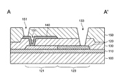
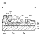
- FIG. 1 is a plan view showing an outline of a diode according to an embodiment of the present invention.
- FIG. 2A is a cross-sectional view showing an outline of a diode according to an embodiment of the present invention.
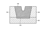
- FIG. 2B is a partially enlarged view of a cross-sectional view showing an outline of a diode according to an embodiment of the present invention.
- the cross-sectional view of FIG. 2A is a cross-sectional view taken along line AA ′ of FIG.
- the enlarged view of FIG. 2B is an enlarged view of the dotted line area of FIG. 2A.
- FIGS. 1 is a plan view showing an outline of a diode according to an embodiment of the present invention.
- FIG. 2A is a cross-sectional view showing an outline of a diode according to an embodiment of the present invention.
- FIG. 2B is a partially enlarged view of a cross-sectional view showing an outline of a diode according to an embodiment of the present
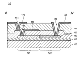
- the diode 10 includes a substrate 100, an underlayer 110, an oxide semiconductor layer 120, an insulating layer 130 (first insulating layer), a conductive layer 140 (first conductive layer), and an insulating layer 150. (Second insulating layer), conductive layer 160 (second conductive layer), and conductive layer 170 are provided.
- the oxide semiconductor layer 120 is provided over the substrate 100.
- the base layer 110 is provided between the substrate 100 and the oxide semiconductor layer 120.
- the oxide semiconductor layer 120 is divided into a first region 121 and a second region 123.
- the oxide semiconductor layer 120 in the second region 123 has lower resistance than the oxide semiconductor layer 120 in the first region 121.
- the insulating layer 130 is provided over the oxide semiconductor layer 120.
- the insulating layer 130 is provided with an opening 131 (first exposed portion) and an opening 133 (second exposed portion).
- the opening 131 exposes the oxide semiconductor layer 120 in the first region 121.
- the opening 133 exposes the oxide semiconductor layer 120 in the second region 123.
- the insulating layer 130 covers the oxide semiconductor layer 120 other than the openings 131 and 133.
- the conductive layer 140 is provided on the insulating layer 130 and inside the opening 131.
- the conductive layer 140 is connected to the oxide semiconductor layer 120 in the first region 121 through the opening 131.
- a low resistance oxide semiconductor layer 125 having a resistance lower than that of the oxide semiconductor layer 120 in the first region 121 is present between the oxide semiconductor layer 120 and the conductive layer 140 in the first region 121. ing.
- the low resistance oxide semiconductor layer 125 reduces the contact resistance between the conductive layer 140 and the oxide semiconductor layer 120.
- the low-resistance oxide semiconductor layer 125 is provided in the region where the oxide semiconductor layer 120 is exposed by the opening 131. In other words, the low resistance oxide semiconductor layer 125 is surrounded by the oxide semiconductor layer 120 whose resistance is higher than that of the low resistance oxide semiconductor layer 125 in plan view.
- the low-resistance oxide semiconductor layer 125 is formed in the vicinity of the surface of the oxide semiconductor layer 120, and may not be observed by analysis such as cross-sectional observation. However, in order to obtain an ohmic contact between the oxide semiconductor layer 120 and the conductive layer 140 in the first region 121 functioning as a channel, the low resistance oxide semiconductor layer 125 is required between them. Therefore, even if the low-resistance oxide semiconductor layer 125 is not observed between the oxide semiconductor layer 120 and the conductive layer 140 in cross-sectional observation, the low-resistance oxide semiconductor layer 125 exists between them. There is a high probability of being
- the first region 121 corresponds to a region overlapping with the conductive layer 140 in the pattern of the oxide semiconductor layer 120 in plan view.
- the second region 123 corresponds to a region where the pattern of the oxide semiconductor layer 120 is exposed from the conductive layer 140 in plan view. That is, the second region 123 corresponds to a region which does not overlap with the conductive layer 140 in the pattern of the oxide semiconductor layer 120.
- the boundary between the first region 121 and the second region 123 is along a part of the pattern end of the conductive layer 140 in plan view.
- the conductive layer 140 overlaps the oxide semiconductor layer 120 in the first region 121 with the insulating layer 130 interposed therebetween.
- the boundary between the first region 121 and the second region 123 coincides with a part of the pattern end of the conductive layer 140 in plan view, but the present invention is not limited to this configuration.
- the boundary between the first region 121 and the second region 123 may be offset from a part of the pattern end of the conductive layer 140.
- the boundary between the first region 121 and the second region 123 may overlap with the conductive layer 140 in plan view.
- the insulating layer 150 is provided on the insulating layer 130 and the conductive layer 140.
- the insulating layer 150 is provided with an opening 151 and an opening 133.
- the opening 151 exposes part of the conductive layer 140.
- the opening 133 exposes the oxide semiconductor layer 120 in the second region 123 as described above.
- an opening provided in both of the insulating layers 130 and 150 is referred to as an opening 133.
- the conductive layer 160 is provided on the insulating layer 150 and in the opening 133. That is, the conductive layer 160 is provided in a layer different from the conductive layer 140.
- the conductive layer 160 is connected to the oxide semiconductor layer 120 in the second region 123 through the opening 133. Referring to FIG. 1, the oxide semiconductor layer 120 in the second region 123 overlaps with the conductive layer 160 in plan view.
- the conductive layer 170 is provided on the insulating layer 150 and inside the opening 151. That is, the conductive layer 170 is provided in the same layer as the conductive layer 160.
- the conductive layer 170 is connected to the conductive layer 140 through the opening 151.
- the diode 10 is a diode-connected transistor.
- the oxide semiconductor layer 120 in the first region 121 corresponds to an active layer.
- the conductive layer 140 provided on the top surface of the insulating layer 130 corresponds to a gate electrode.
- the insulating layer 130 between the oxide semiconductor layer 120 and the conductive layer 140 corresponds to a gate insulating layer.
- the conductive layer 140 in contact with the oxide semiconductor layer 120 in the opening 131 corresponds to a source electrode.
- the conductive layer 160 corresponds to a drain electrode. That is, the diode 10 is a transistor in which the source electrode and the gate electrode are connected. In the diode 10, the source electrode and the drain electrode may be switched.
- the oxide semiconductor layer 120 is an n-type semiconductor is described.
- the gate electrode and the source electrode are supplied with a potential higher than that of the drain electrode, so that this transistor is turned on. Therefore, current flows from conductive layer 140 to conductive layer 160.
- the potential of the conductive layer 140 is lower than the potential of the conductive layer 160, a potential lower than that of the drain electrode is supplied to the gate electrode and the source electrode, so that this transistor is turned off. That is, the diode 10 has a rectifying function.
- the leakage current in the OFF state of the transistor in which the oxide semiconductor layer 120 is used as the active layer is much smaller than the leakage current in the OFF state of a transistor in which a general semiconductor layer such as silicon is used as the active layer. . Therefore, almost no current flows even if a reverse bias is applied to the diode 10. As a result, the excellent rectifying action of the diode 10 is obtained.
- the substrate 100 a substrate having transparency to visible light is used.
- a rigid substrate having no flexibility and a flexible substrate having flexibility are used.
- a glass substrate, a quartz substrate, and a sapphire substrate may be used as a rigid substrate.
- a polyimide substrate, an acrylic substrate, a siloxane substrate, and a fluorine resin substrate may be used as a substrate 100.
- a substrate which does not have translucency may be used as the substrate 100.
- a semiconductor substrate such as a silicon substrate, a silicon carbide substrate, or a compound semiconductor substrate, or a conductive substrate such as a stainless steel substrate may be used.
- the base layer 110 a material whose adhesion between the substrate 100 and the oxide semiconductor layer 120 is improved, and a material which prevents impurities from reaching the oxide semiconductor layer 120 from the substrate 100 are used.
- a structure in which these are stacked may be used as the base layer 110.
- the base layer 110 is omitted. It is also good.
- a TEOS layer or an organic insulating material may be used in addition to the above-described inorganic insulating material.
- SiO x N y and AlO x N y are silicon compounds and aluminum compounds containing nitrogen (N) in a smaller amount than oxygen (O).
- SiN x O y and AlN x O y are silicon compounds and aluminum compounds that contain less oxygen than nitrogen.
- the base layer 110 exemplified above may be formed by physical vapor deposition (PVD) or may be formed by chemical vapor deposition (CVD).
- PVD physical vapor deposition
- CVD chemical vapor deposition
- a sputtering method a vacuum evaporation method, an electron beam evaporation method, a molecular beam epitaxy method and the like are used.
- CVD method a thermal CVD method, a plasma CVD method, a catalytic CVD method (Cat (Catalytic) -CVD method or a hot wire CVD method) or the like is used.
- the TEOS layer refers to a CVD layer using TEOS (Tetra Ethyl Ortho Silicate) as a raw material.
- the organic insulating material polyimide resin, acrylic resin, epoxy resin, silicone resin, fluorine resin, siloxane resin or the like is used.
- the underlayer 110 may be a single layer or may be a stack of the above materials.
- the base layer 110 may be a stack of an inorganic insulating material and an organic insulating material.
- the oxide semiconductor layer 120 a metal oxide having semiconductor characteristics is used.
- an oxide semiconductor containing indium (In), gallium (Ga), zinc (Zn), and oxygen (O) may be used.
- the oxide semiconductor containing In, Ga, Zn, and O used in one embodiment of the present invention is not limited to the above composition ratio, and an oxide semiconductor having a composition ratio different from the above may be used.
- an oxide semiconductor with a high ratio of In to the above ratio may be used as the oxide semiconductor layer 120 in order to improve mobility.
- an oxide semiconductor in which the ratio of Ga to the above ratio is large may be used as the oxide semiconductor layer 120 so that the band gap is increased.
- oxide semiconductor containing In, Ga, Zn, and O may be added to the above oxide semiconductor.
- a metal element such as Al or Sn may be added to the above oxide semiconductor.
- zinc oxide (ZnO), nickel oxide (NiO), tin oxide (SnO 2 ), titanium oxide (TiO 2 ), vanadium oxide (VO 2 ), indium oxide (In 2 O 3 ), Strontium titanate (SrTiO 3 ) or the like may be used as the oxide semiconductor layer 120.
- the oxide semiconductor layer 120 may be amorphous or crystalline.
- the oxide semiconductor layer 120 may be a mixed phase of amorphous and crystal.
- the oxide semiconductor layer 120 is formed by PVD.
- silicon (Si), gallium (Ga), gallium arsenide (GaAs), gallium nitride (GaN), silicon carbide (SiC) can be used as the semiconductor layer. May be used.
- an inorganic insulating material such as SiO x , SiO x N y , SiN x , SiN x O y , AlO x , AlO x N y , AlN x , or AlN x O y is used.
- the insulating layers 130 and 150 are formed in the same manner as the base layer 110.
- the insulating layers 130 and 150 may be a single layer or may be a stack of the above materials.
- the insulating layers 130 and 150 may be the same material as the base layer 110 or may be different materials.
- the insulating layer 130 and the insulating layer 150 may be the same material as each other or different materials.
- the insulating layer 130 in contact with the oxide semiconductor layer 120 preferably contains a large amount of excess oxygen.
- the insulating layer 130 is an oxide insulating layer in which the proportion of oxygen is higher than the proportion of oxygen in the stoichiometric ratio of the material used for the insulating layer 130, and it is preferable to release oxygen by heat treatment.
- the oxygen in the insulating layer 130 has dangling bonds, and the bond is broken at an energy lower than the bonding energy in the stoichiometry of the material used for the insulating layer 130. Since oxygen in the insulating layer 130 has dangling bonds, the oxide semiconductor layer 120 in the second region 123 contains many defects.
- a common metal material or conductive semiconductor material is used as the conductive layers 140, 160, 170.
- the conductive layers 140, 160, and 170 aluminum (Al), titanium (Ti), chromium (Cr), cobalt (Co), nickel (Ni), zinc (Zn), molybdenum (Mo), indium (In) Tin (Sn), hafnium (Hf), tantalum (Ta), tungsten (W), platinum (Pt), bismuth (Bi) or the like is used. Alloys of the above materials may be used as the conductive layers 140, 160, and 170, and nitrides of the above materials may be used.
- the above conductive layer is formed by PVD.
- conductive oxide such as ITO (indium tin oxide), IGO (indium gallium oxide), IZO (indium zinc oxide), GZO (zinc oxide with gallium added as a dopant), etc.
- An object semiconductor may be used.
- the conductive layers 140, 160, and 170 may be single layers or may be stacked layers of the above materials. Note that a material used as the conductive layer 140 and in contact with the oxide semiconductor layer 120 in the first region 121 reduces oxygen in the oxide semiconductor layer 120 to reduce the resistance of the surface of the oxide semiconductor layer 120. It is possible to use a material whose oxide is not insulating.
- the diode 10 which concerns on 1st Embodiment of this invention, the diode 10 can be comprised with the diode connection transistor of simpler structure.
- the above diode 10 is a liquid crystal display (LCD), a self light emitting display using a self light emitting element (Organic Light-Emitting Diode: OLED) such as an organic EL element or a quantum dot in a display portion, or In a reflective display device such as electronic paper, it is used for each pixel and drive circuit of each display device.
- OLED Organic Light-Emitting Diode
- the above-described diode 10 is not limited to one used in a display device, and may be used in, for example, an integrated circuit (IC) such as a microprocessor (Micro-Processing Unit: MPU).
- IC integrated circuit
- MPU Micro-Processing Unit
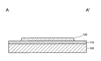
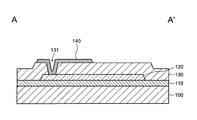
- FIGS. 3 to 7 are cross-sectional views showing a method of manufacturing a diode according to an embodiment of the present invention.
- the base layer 110 is formed over the substrate 100, and the oxide semiconductor layer 120 is formed over the base layer 110.
- a pattern of the oxide semiconductor layer 120 shown in FIG. 3 is formed on the oxide semiconductor layer 120 formed over the entire surface of the substrate 100 by photolithography and etching. The formation of the pattern shown below is carried out by photolithography and etching unless otherwise stated. However, for each of photolithography and etching, conditions suitable for the respective steps are adopted.
- the oxide semiconductor layer 120 can be formed by a sputtering method.
- the etching of the oxide semiconductor layer 120 may be dry etching or wet etching.
- an etchant containing oxalic acid can be used.
- the insulating layer 130 is formed over the oxide semiconductor layer 120.
- the opening 131 is formed in the insulating layer 130 to expose part of the oxide semiconductor layer 120 in the first region 121 described later.
- the conductive layer 140 is formed on the insulating layer 130 and in the opening 131.
- oxygen in the vicinity of the surface of the oxide semiconductor layer 120 is reduced by the formed conductive layer 140.
- the low-resistance oxide semiconductor layer 125 is formed in the vicinity of the surface of the oxide semiconductor layer 120 exposed by the opening 131.
- the conductive layer 140 formed on the bottom of the opening 131 is oxidized by the oxygen transferred from the oxide semiconductor layer 120. Therefore, as a material of the conductive layer 140, a material which does not lose conductivity even when oxidized is preferably used.
- a region overlapping with the oxide semiconductor layer 120 and the conductive layer 140 in a plan view is a first region 121 described later.
- an impurity is introduced into the oxide semiconductor layer 120 from above the oxide semiconductor layer 120 (the side on which the conductive layer 140 is formed with respect to the oxide semiconductor layer 120).
- the introduction of the impurity is performed by ion doping or ion implantation.
- the impurity is blocked by the conductive layer 140 in a region where the oxide semiconductor layer 120 and the conductive layer 140 overlap in plan view; therefore, the oxide semiconductor layer 120 is not reached.
- the impurity is not blocked by the conductive layer 140 and reaches the oxide semiconductor layer 120.
- a region where an impurity is not introduced into the oxide semiconductor layer 120 is a first region 121.
- a region where an impurity is introduced to the oxide semiconductor layer 120 is a second region 123.
- the first region 121 is a region where the oxide semiconductor layer 120 and the conductive layer 140 overlap in plan view.
- the second region 123 is a region where the oxide semiconductor layer 120 is exposed from the conductive layer 140 in plan view.
- FIG. 6 the configuration in which the boundary between the first region 121 and the second region 123 coincides with a part of the pattern end of the conductive layer 140 is illustrated.
- the impurity implanted toward the oxide semiconductor layer 120 is also implanted to the inside of the pattern of the conductive layer 140 rather than the pattern edge of the conductive layer 140. Therefore, the boundary between the first region 121 and the second region 123 may overlap with the conductive layer 140 in plan view.
- the resistance of the oxide semiconductor layer 120 in the second region 123 is lower than the resistance of the oxide semiconductor layer 120 in the first region 121.
- materials used in a general semiconductor manufacturing process such as boron (B), phosphorus (P), and argon (Ar) are used.
- the insulating layer 150 is formed on the insulating layer 130 and the conductive layer 140.
- the opening 151 is formed in the insulating layer 150 to expose part of the conductive layer 140.
- the opening 133 is formed in the insulating layers 130 and 150, and a part of the oxide semiconductor layer 120 in the second region 123 is exposed.
- the process of opening the insulating layers 130 and 150 collectively is illustrated, but the present invention is not limited to this process.
- an opening may be formed in the insulating layer 150 to expose a part of the insulating layer 130, and the insulating layer 130 may be opened by a method different from the opening of the insulating layer 150.
- the diode 10 according to the first embodiment can be formed by the manufacturing method described above.
- the oxide semiconductor layer 120 is doped with the conductive layer 140 corresponding to the gate electrode and the source electrode of the diode-connected transistor as a mask.
- the position of the boundary between the first area 121 and the second area 123 can be determined with high accuracy.
- the conductive layer 140 is formed over the oxide semiconductor layer 120 exposed in the opening 131, the surface of the oxide semiconductor layer 120 is reduced in resistance by the conductive layer 140. Therefore, in the region where the oxide semiconductor layer 120 and the conductive layer 140 are in contact with each other, it is not necessary to provide a low resistance region in the oxide semiconductor layer 120 in advance. That is, the diode 10 can be manufactured by a simpler manufacturing method.
- FIG. 8 is a cross-sectional view showing an outline of a diode according to an embodiment of the present invention.
- the diode 10A shown in FIG. 8 is similar to the diode 10 shown in FIG. 2A.
- the diode 10A is different from the diode 10 in that the thickness of the insulating layer 130A in the second region 123A is smaller than the thickness of the insulating layer 130A in the first region 121A.
- the thickness of the insulating layer 130A exposed from the conductive layer 140A in plan view is smaller than the thickness of the insulating layer 130A overlapping the conductive layer 140A.
- the thickness of the insulating layer 130A in the second region 123A may be 10 nm or more.
- the insulating layer 130A of the diode 10A shown in FIG. 8 can be obtained by over-etching the insulating layer 130 using the conductive layer 140 as a mask in the process of FIG.
- the impurity can be introduced with small energy in the step of impurity introduction shown in FIG.
- the film thickness of the insulating layer 130 in the second region 123 is large, it is necessary to accelerate the impurity with high energy in order to introduce the impurity.
- part of the high-energy accelerated impurity may pass through the conductive layer 140 and the insulating layer 130 below the conductive layer 140 to reach the oxide semiconductor layer 120 in the first region 121.
- a leak current flows when a reverse bias voltage is supplied to the diode 10.
- the diode 10A according to the second embodiment of the present invention the same effect as the diode 10 according to the first embodiment can be obtained. Furthermore, in the case of the diode 10A illustrated in FIG. 8, an impurity can be introduced into the oxide semiconductor layer 120A in the second region 123A with low energy. Therefore, the introduction of an unintended impurity into the oxide semiconductor layer 120A in the first region 121A can be suppressed.
- FIG. 9 is a cross-sectional view showing an outline of a diode according to an embodiment of the present invention.
- the diode 10B shown in FIG. 9 is similar to the diode 10 shown in FIG. 2A. However, the diode 10B is different from the diode 10 in that the insulating layer 130B in the second region 123B is removed, and the insulating layer 150B is in contact with the oxide semiconductor layer 120B in the second region 123B. In other words, the oxide semiconductor layer 120B in the second region 123B is exposed from the insulating layer 130B.
- the physical properties of the insulating layer 150B are different from the physical properties of the insulating layer 130B.
- the insulating layer 130B an oxide insulating layer in which the ratio of containing oxygen is higher than the ratio of oxygen in the stoichiometric ratio of the material used for the insulating layer 130B can be used.
- SiO x or SiO x N y which has a higher proportion of oxygen than the proportion of oxygen in the stoichiometric ratio of the following materials, can be used.
- the insulating layer 150B an oxide insulating layer in which the ratio of containing oxygen is smaller than the ratio of oxygen in the stoichiometric ratio of the material used for the insulating layer 150B can be used.
- a material which releases hydrogen or ammonia by heat treatment can be used as the insulating layer 150B.
- SiN x and SiN x O y can be used as the insulating layer 150B.
- the step of introducing an impurity into the oxide semiconductor layer 120B in contact with the insulating layer 150B is provided because the insulating layer 150B releases oxygen more easily than the insulating layer 130B and hydrogen and ammonia are easily released. Accordingly, the resistance of the oxide semiconductor layer 120B in the second region 123B can be reduced.
- FIGS. 10 to 12 are cross-sectional views showing a method of manufacturing a diode according to an embodiment of the present invention.
- the description will be omitted.
- the insulating layer 130B is etched using the conductive layer 140B as a mask to expose the oxide semiconductor layer 120B.
- the present invention is not limited to this manufacturing method.
- the pattern of the oxide semiconductor layer 120B may be formed after the pattern of the conductive layer 140B.
- the oxide semiconductor layer 120B can function as an etching stopper in etching for exposing the oxide semiconductor layer 120B.
- the insulating layer 150B is formed on the insulating layer 130B and the conductive layer 140B, and on the oxide semiconductor layer 120B exposed from the insulating layer 130B and the conductive layer 140B.
- the oxide semiconductor layer 120B in the second region 123B is exposed from the insulating layer 130B. Therefore, when forming the insulating layer 150B, the oxide semiconductor layer 120B in the second region 123B is exposed to the film formation environment of the insulating layer 150B.
- oxygen in the vicinity of the surface of the oxide semiconductor layer 120B is reduced, and oxygen vacancies are generated in the oxide semiconductor layer 120B. As a result, the resistance of the oxide semiconductor layer 120B in the second region 123B is reduced.
- the film formation of the insulating layer 150B may be performed under film formation conditions using a large amount of silane. That is, regarding the ratio of silane to gas other than silane, the ratio of silane used for film formation of the insulating layer 150B is higher than the ratio of silane used for film formation of other insulating layers (eg, the underlayer 110B and the insulating layer 130B). It may be high. By forming the insulating layer 150B under the condition that the ratio of silane is high, the insulating layer 150B with high concentration of hydrogen in the film can be formed.
- the layer structure of the insulating layer 150B is not particularly limited, but may be, for example, a laminated structure in which SiN x is formed on SiO x .
- Heat treatment may be performed after the insulating layer 150B is formed.
- hydrogen contained in the insulating layer 150B is diffused into the oxide semiconductor layer 120B.
- oxygen vacancy is generated in the oxide semiconductor layer 120B in the second region 123B.
- the resistance of the oxide semiconductor layer 120B in the second region 123B is reduced.
- an opening 151B is formed in the insulating layer 150B to expose a part of the conductive layer 140B.
- the opening 153B is formed in the insulating layer 150B, and part of the oxide semiconductor layer 120 in the second region 123 is exposed.
- the thicknesses of the insulating layers of the openings 151B and 153B are substantially the same, processing control of the openings 151B and 153B is easy.
- conductive layers are formed on the insulating layer 150B, inside the opening 153B, and inside the opening 151B and processed to form the conductive layers 160B and 170B shown in FIG.
- the diode 10B according to the first embodiment can be formed by the manufacturing method described above.
- the same effect as the diode 10 according to the first embodiment can be obtained. Furthermore, in the case of the diode 10B illustrated in FIG. 9, the insulating layer 150B is formed to be in contact with the oxide semiconductor layer 120B in the second region 123B, thereby reducing the resistance of the oxide semiconductor layer 120B in the second region 123B. Can be That is, since there is no need to introduce impurities, the manufacturing process can be shortened.
- FIG. 13 is a plan view showing an outline of a diode according to an embodiment of the present invention.
- the diode 10C shown in FIG. 13 is similar to the diode 10 shown in FIG. However, the diode 10C is different from the diode 10 in that the pattern end of the oxide semiconductor layer 120C surrounds the pattern end of the conductive layer 140C in plan view. In other words, the first area 121C is surrounded by the second area 123C.
- the oxide semiconductor layer 120C in the first region 121C functions as a channel of the diode 10C. However, in the configuration in FIG. 13, the pattern end of the oxide semiconductor layer 120 ⁇ / b> C does not function as a channel.
- the configuration of the transistor 20D according to the present embodiment is a configuration in which a gate insulating layer and a gate electrode are added to the configuration of the diode 10 according to the first embodiment.
- the same portions as the above embodiment or portions having similar functions are denoted by the same numerals or numerals appended with an alphabet after the same numerals, and the repeated description thereof is omitted. Do.
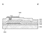
- FIG. 14 is a plan view showing an outline of a transistor according to an embodiment of the present invention.
- FIG. 15 is a cross-sectional view showing an outline of a transistor according to an embodiment of the present invention.
- the transistor 20D shown in FIGS. 14 and 15 is similar to the diode 10 shown in FIGS. 1 and 2A. However, the transistor 20D is different from the diode 10 in that the gate electrode 200D (third conductive layer) is provided at a position corresponding to the oxide semiconductor layer 120D in the first region 121D.
- a gate insulating layer 210D (third insulating layer) is provided between the oxide semiconductor layer 120D and the gate electrode 200D.
- the gate electrode 200D overlaps with the oxide semiconductor layer 120D of the first region 121D and the oxide semiconductor layer 120D of at least a part of the second region 123D.
- the boundary between the first region 121D and the second region 123D is on the inner side of the pattern of the gate electrode 200D than the pattern end of the gate electrode 200D.
- the gate electrode 200D is not limited to the above-described structure, and may be provided in a region that continuously connects at least the opening 131D and the second region 123D.
- the gate electrode 200D may overlap with the oxide semiconductor layer 120D in both the first region 121D and the second region 123D. That is, the pattern end of the oxide semiconductor layer 120D including the first region 121D and the second region 123D may be surrounded by the pattern end of the gate electrode 200D.
- the transistor 20D when the voltage (ON voltage) for generating carriers in the oxide semiconductor layer 120D in the first region 121D is supplied to the gate electrode 200D, the transistor 20D proceeds in the forward direction from the conductive layer 140D to the conductive layer 160D, In addition, current flows in two directions in the opposite direction from the conductive layer 160D to the conductive layer 140D.
- a reverse bias is supplied so that current flows in the reverse direction
- carriers generated by the gate electrode 200D are present in the oxide semiconductor layer 120D of the first region 121D.
- the oxide semiconductor layer 120D in the first region 121D includes the carriers generated by the conductive layer 140 in addition to the carriers generated by the gate electrode 200D.
- the current flowing in the forward direction is larger than the current flowing in the reverse direction. In other words, even when the same voltage is supplied to the gate electrode 200D, the amount of current flowing to the transistor 20D varies depending on the direction of the current.
- the gate electrode 200D in the oxide semiconductor layer 120D in the first region 121D current flows in the forward direction but does not flow in the reverse direction. That is, when the OFF voltage is supplied to the gate electrode 200D, the transistor 20D functions as a diode. In other words, the gate electrode 200D switches the function of the transistor 20D to a transistor or a diode.
- the gate electrode 200D and the gate insulating layer 210D are provided under the diode 10 of the first embodiment is illustrated in the present embodiment, the gate electrode and the gate insulation of the diodes of the second to fourth embodiments are illustrated. A layer may be provided.
- the transistor 20D according to the fifth embodiment can provide a transistor having a high ON current in one direction. Further, in the transistor 20D, the function of the transistor and the function of the diode are switched by the voltage supplied to the gate electrode 200D.
- FIG. 16 to FIG. 21 are cross-sectional views showing a method of manufacturing a transistor according to an embodiment of the present invention.
- a base layer 110D is formed on a substrate 100D, and a pattern of a gate electrode 200D is formed on the base layer 110D.
- the gate insulating layer 210D is formed over the gate electrode 200D and the base layer 110D, and the oxide semiconductor layer 120D is formed over the gate insulating layer 210D.
- the insulating layer 130D is formed over the oxide semiconductor layer 120D.
- An opening 131D is formed in the insulating layer 130D to expose part of the oxide semiconductor layer 120D in a first region 121D described later.
- the conductive layer 140D is formed on the insulating layer 130D and in the opening 131D. As described above, when the conductive layer 140D is formed on the oxide semiconductor layer 120D exposed by the opening 131D, oxygen in the vicinity of the surface of the oxide semiconductor layer 120D is reduced by the formed conductive layer 140D. . As a result, a low-resistance oxide semiconductor layer whose resistance is lower than that of the oxide semiconductor layer 120D is formed between the oxide semiconductor layer 120D and the conductive layer 140D. As shown in FIG. 19, the pattern end of the conductive layer 140D is located more inside the pattern of the gate electrode 200D than the pattern end of the gate electrode 200D.
- an impurity is introduced into the oxide semiconductor layer 120D from above the oxide semiconductor layer 120D (the side on which the conductive layer 140D is formed with respect to the oxide semiconductor layer 120D).
- the introduction of the impurity is performed by ion doping or ion implantation.
- the impurity is blocked by the conductive layer 140D and does not reach the oxide semiconductor layer 120D in a region where the oxide semiconductor layer 120D and the conductive layer 140D overlap in plan view.
- the impurity is not blocked by the conductive layer 140D and reaches the oxide semiconductor layer 120D.
- the pattern end of the conductive layer 140D is located more inside the pattern of the gate electrode 200D than the pattern end of the gate electrode 200D. Therefore, in plan view, the oxide semiconductor layer 120D in the first region 121D overlaps with the gate electrode 200D. That is, in the transistor 20D, the region where carriers are generated by the voltage supplied to the gate electrode 200D continuously connects the opening 131D and the oxide semiconductor layer 120D in the second region 123D.
- the insulating layer 150D is formed on the insulating layer 130D.
- An opening 151D is formed in the insulating layer 150D to expose part of the conductive layer 140D.
- the opening 133D is formed in the insulating layers 130D and 150D, and a part of the oxide semiconductor layer 120D in the second region 123D is exposed.
- the process of opening the insulating layers 130D and 150D collectively is illustrated, but the present invention is not limited to this process.
- an opening may be formed in the insulating layer 150D to expose a part of the insulating layer 130D, and the insulating layer 130D may be opened by a method different from the opening of the insulating layer 150D.
- the transistor 20D according to the fifth embodiment can be formed by the manufacturing method described above.
- the transistor 20D is manufactured by a simpler manufacturing method, as in the method of manufacturing the diode 10 according to the first embodiment. Can.
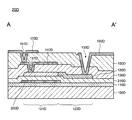
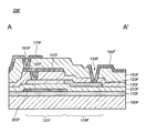
- FIG. 22 is a cross-sectional view showing an outline of a transistor according to an embodiment of the present invention.
- the transistor 20F shown in FIG. 22 is similar to the transistor 20D shown in FIG. However, the transistor 20F is different from the transistor 20D in that the thickness of the insulating layer 130F in the second region 123F is smaller than the thickness of the insulating layer 130F in the first region 121F.
- the thickness of the insulating layer 130F exposed from the conductive layer 140F in plan view is smaller than the thickness of the insulating layer 130F overlapping with the conductive layer 140F.
- the thickness of the insulating layer 130F in the second region 123F may be 10 nm or more.
- the transistor 20F shown in FIG. 22 can be formed by the same method as the diode 10A shown in FIG.
- the transistor 20F according to the sixth embodiment of the present invention can obtain the same effect as the transistor 20D according to the fifth embodiment. Furthermore, in the case of the transistor 20F, an impurity can be introduced to the oxide semiconductor layer 120F in the second region 123F with low energy as in the diode 10A. Accordingly, the introduction of an unintended impurity into the oxide semiconductor layer 120F in the first region 121F can be suppressed.
- FIG. 23 is a cross-sectional view showing an outline of a transistor according to an embodiment of the present invention.
- the transistor 20G shown in FIG. 23 is similar to the transistor 20D shown in FIG. However, the transistor 20G is different from the transistor 20D in that the insulating layer 130G in the second region 123G is removed, and the insulating layer 150G is in contact with the oxide semiconductor layer 120G in the second region 123G. In other words, the oxide semiconductor layer 120G in the second region 123G is exposed from the insulating layer 130G.
- the physical properties of the insulating layer 150G are different from the physical properties of the insulating layer 130G.
- an oxide insulating layer in which the ratio of containing oxygen is higher than the ratio of oxygen in the stoichiometric ratio of the material used for the insulating layer 130G can be used.
- SiO x or SiO x N y which has a higher proportion of oxygen than the proportion of oxygen in the stoichiometry of the materials below, can be used.
- the insulating layer 150G an oxide insulating layer in which the ratio of containing oxygen is smaller than the ratio of oxygen in the stoichiometric ratio of the material used for the insulating layer 150G can be used.
- a material which releases hydrogen or ammonia by heat treatment can be used as the insulating layer 150G.
- SiN x or SiN x O y can be used as the insulating layer 150G.
- the step of introducing an impurity into the oxide semiconductor layer 120G in contact with the insulating layer 150G is provided because the insulating layer 150G releases oxygen more easily than the insulating layer 130G and hydrogen and ammonia are easily released. Accordingly, the resistance of the oxide semiconductor layer 120G in the second region 123G can be reduced.
- the transistor 20G shown in FIG. 23 can be formed by the same method as the diode 10B shown in FIG. According to the transistor 20G of the seventh embodiment of the present invention, the same effect as that of the transistor 20D of the fifth embodiment can be obtained. Furthermore, in the case of the transistor 20G, the resistance of the oxide semiconductor layer 120G in the second region 123G can be reduced by forming the insulating layer 150G in contact with the oxide semiconductor layer 120G in the second region 123G. it can. That is, since there is no need to introduce impurities, the manufacturing process can be shortened.
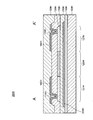
- FIG. 24 is a cross-sectional view showing an outline of a transistor according to an embodiment of the present invention.
- the transistor 20H shown in FIG. 24 is a transistor in which the transistors 20D shown in FIG. 15 are connected to face each other.
- the oxide semiconductor layer 120H is divided in the order of a first region 121H, a second region 123H, and a third region 127H.
- the oxide semiconductor layer 120H in the third region 127H has a higher resistance than the oxide semiconductor layer 120H in the second region 123H, similarly to the oxide semiconductor layer 120H in the first region 121H. That is, the resistance of the oxide semiconductor layer 120H in the third region 127H is substantially the same as the resistance of the oxide semiconductor layer 120H in the first region 121H.
- the second region 123H of the oxide semiconductor layer 120H is provided between the first region 121H and the third region 127H.
- the gate electrode 200H is provided to correspond to the oxide semiconductor layer 120H in the first region 121H, the second region 123H, and the third region 127H.
- the conductive layer 142H is provided corresponding to the first region 121H. That is, in a plan view, the first region 121H is a region overlapping with the conductive layer 142H.
- the conductive layer 144H is provided corresponding to the third region 127H. That is, in plan view, the third region 127H is a region overlapping with the conductive layer 144H.
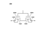
- FIG. 25 is a circuit diagram of the transistor shown in FIG.
- the transistor 20H is a transistor in which two diode-connected transistors are connected in series so as to face each other.
- the two transistors When an ON voltage is supplied to the gate electrode 200H, the two transistors are in the ON state, and function as normal transistors that can flow current in both directions of the conductive layers 142H and 144H.
- an OFF voltage is supplied to the gate electrode 200H, the two transistors are in the OFF state, and both function as diodes.
- the transistor 20H functions as a circuit in which diodes facing in opposite directions are connected in series.
- the transistor 20H can switch between the function of the transistor and the function of the diode by the voltage supplied to the gate electrode 200H.
- the circuit shown in FIG. 26 can be used, for example, as a protective circuit which protects the circuit from static electricity or the like.
- the transistor 20H according to the eighth embodiment can provide a transistor whose function can be switched by the voltage supplied to the gate electrode 200H.
- the above transistors 20D, 20F, 20G, and 20H are used for each pixel and drive circuit of each display device in a self light emitting display device using LCD, OLED, or a reflection type display device such as electronic paper.
- the above-described transistor is not limited to one used in a display device, and may be used, for example, in an IC such as an MPU.
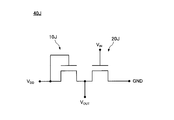
- the ninth embodiment The outline of the logic circuit 40J according to the ninth embodiment of the present invention will be described with reference to FIG.
- the same parts or parts having the same functions as those in the above embodiments are given the same numerals or numerals appended with an alphabet after the same numerals, and repeated descriptions thereof Is omitted.
- a logic circuit 40J shown in FIG. 27 is an inverter circuit using a diode 10J and a transistor 20J.
- the source electrode of the diode 10J is connected to the power supply voltage V DD .
- the source electrode of the transistor 20J is connected to GND.
- the input signal V IN is supplied to the gate electrode of the transistor 20J.
- An output signal V.sub.OUT is output from the diode 10J and the drain electrode of the transistor 20J.
- the diodes of the first to fourth embodiments can be used as the diode 10J.
- a general transistor is used as the transistor 20J, but the transistors of the fifth to eighth embodiments can also be used.
- the above logic circuit 40J is used for each pixel and drive circuit of each display device in a self light emitting display device using LCD, OLED, or a reflection type display device such as electronic paper.
- the above-described logic circuit is not limited to one used in a display device, and may be used, for example, in an IC such as an MPU.
Landscapes
- Engineering & Computer Science (AREA)
- Physics & Mathematics (AREA)
- Computer Hardware Design (AREA)
- General Physics & Mathematics (AREA)
- Theoretical Computer Science (AREA)
- Thin Film Transistor (AREA)
Abstract
簡易的な構造および製造方法のダイオードが提供される。ダイオードは、第1領域および前記第1領域よりも低抵抗の第2領域を有する半導体層と、前記第1領域の前記半導体層に達する第1開口部、および前記第2領域の前記半導体層に達する第2開口部が設けられ、前記第1開口部および前記第2開口部以外の前記半導体層を覆う第1絶縁層と、前記第1開口部において前記半導体層に接続され、平面視において前記第1絶縁層を介して前記第1領域の前記半導体層と重畳する第1導電層と、前記第2開口部において前記半導体層に接続された第2導電層と、を有する。
Description
本発明は、ダイオード、トランジスタ、およびこれらを有する表示装置に関する。
近年、表示装置やパーソナルコンピュータなどの駆動回路に用いられる微細なスイッチング素子として、トランジスタ、ダイオードなどの半導体装置が用いられている。トランジスタは、映像を表示する画素回路、および画素回路を駆動する駆動回路などに用いられている。ダイオードは、静電気等から回路を保護する保護回路、および電源から供給された電圧を昇圧するチャージポンプ回路などに用いられている。トランジスタおよびダイオードを効率よく製造するために、例えば特許文献1に示すように、ダイオードとしてドレイン端子とゲート端子とが接続されたトランジスタ(ダイオード接続トランジスタ)が用いられている。
ダイオード接続トランジスタは、一般的なトランジスタのゲート端子とソース端子、またはゲート端子とドレイン端子とを接続することで製造される。つまり、ダイオードを製造するためには、トランジスタを製造する場合と同じ数の工程が必要である。
本発明に係る一実施形態は、上記実情に鑑み、簡易的な構造および簡易的な製造方法のダイオード、トランジスタ、およびこれらを有する表示装置を提供することを目的とする。
本発明の一実施形態によるダイオードは、第1領域および前記第1領域よりも低抵抗の第2領域を有する半導体層と、前記第1領域の前記半導体層を露出する第1開口部、および前記第2領域の前記半導体層を露出する第2開口部を有し、前記第1開口部および前記第2開口部以外の前記半導体層を覆う第1絶縁層と、前記第1開口部において前記半導体層に接続され、平面視において前記第1絶縁層を介して前記第1領域の前記半導体層と重畳する第1導電層と、前記第2開口部において前記半導体層に接続された第2導電層と、を有する。
本発明の一実施形態によるトランジスタは、第1領域および前記第1領域よりも低抵抗の第2領域を有する半導体層と、前記第1領域の前記半導体層を露出する第1開口部、および前記第2領域の前記半導体層を露出する第2開口部を有し、前記第1開口部および前記第2開口部以外の前記半導体層を覆う第1絶縁層と、前記第1開口部において前記半導体層に接続され、平面視において前記第1絶縁層を介して前記第1領域の前記半導体層と重畳する第1導電層と、前記第2開口部において前記半導体層に接続された第2導電層と、前記半導体層に対向する、前記半導体層の下の第3導電層と、前記半導体層と前記第3導電層との間の第3絶縁層と、を有する。
以下に、本発明の各実施の形態について、図面を参照しつつ説明する。なお、開示はあくまで一例にすぎない。当業者が、発明の主旨を保ったまま適宜変更することで、容易に想到し得る構成は、当然に本発明の範囲に含有される。図面は説明をより明確にするため、実際の態様に比べ、各部の幅、厚さ、形状等が模式的に表される場合がある。ただし、これはあくまで一例であって、本発明の解釈を限定するものではない。本明細書と各図において、既出の図に関して前述したものと同様の要素には、同一の符号の後にアルファベットを付して、詳細な説明を適宜省略することがある。
本発明の各実施の形態において、基板からダイオードに向かう方向または基板からトランジスタに向かう方向を上または上方という。逆に、ダイオードから基板に向かう方向またはトランジスタから基板に向かう方向を下または下方という。このように、説明の便宜上、上方または下方という語句を用いて説明する。しかし、例えば、基板とダイオードとの上下関係または基板とトランジスタとの上下関係が図示と逆になるように配置されてもよい。以下の説明で、例えば第1部材の上の第2部材という表現は、上記のように第1部材と第2部材との上下関係を説明しているに過ぎず、第1部材と第2部材との間に他の部材が配置されていてもよい。
本明細書において「αはA、BまたはCを含む」、「αはA,BおよびCのいずれかを含む」、「αはA,BおよびCからなる群から選択される一つを含む」、といった表現は、特に明示が無い限り、αがA~Cの複数の組み合わせを含む場合を排除しない。さらに、これらの表現は、αが他の要素を含む場合も排除しない。
〈第1実施形態〉
図1~図7を用いて、本発明の第1実施形態に係るダイオード10の概要について説明する。第1実施形態のダイオード10では、ダイオード接続されたトランジスタの活性層として酸化物半導体層が用いられた構成を例示するが、活性層として酸化物半導体層以外に一般的な半導体層が用いられてもよい。
図1~図7を用いて、本発明の第1実施形態に係るダイオード10の概要について説明する。第1実施形態のダイオード10では、ダイオード接続されたトランジスタの活性層として酸化物半導体層が用いられた構成を例示するが、活性層として酸化物半導体層以外に一般的な半導体層が用いられてもよい。
[ダイオード10の構造]
図1は、本発明の一実施形態に係るダイオードの概要を示す平面図である。図2Aは、本発明の一実施形態に係るダイオードの概要を示す断面図である。図2Bは、本発明の一実施形態に係るダイオードの概要を示す断面図の部分拡大図である。図2Aの断面図は、図1のA-A’線の断面図である。図2Bの拡大図は、図2Aの点線領域を拡大した図である。図1および図2Aに示すように、ダイオード10は、基板100、下地層110、酸化物半導体層120、絶縁層130(第1絶縁層)、導電層140(第1導電層)、絶縁層150(第2絶縁層)、導電層160(第2導電層)、および導電層170を有する。
図1は、本発明の一実施形態に係るダイオードの概要を示す平面図である。図2Aは、本発明の一実施形態に係るダイオードの概要を示す断面図である。図2Bは、本発明の一実施形態に係るダイオードの概要を示す断面図の部分拡大図である。図2Aの断面図は、図1のA-A’線の断面図である。図2Bの拡大図は、図2Aの点線領域を拡大した図である。図1および図2Aに示すように、ダイオード10は、基板100、下地層110、酸化物半導体層120、絶縁層130(第1絶縁層)、導電層140(第1導電層)、絶縁層150(第2絶縁層)、導電層160(第2導電層)、および導電層170を有する。
まず、図2Aを用いて、ダイオード10の断面構造について説明する。酸化物半導体層120は基板100の上に設けられている。下地層110は基板100と酸化物半導体層120との間に設けられている。酸化物半導体層120は第1領域121および第2領域123に区分される。第2領域123の酸化物半導体層120は第1領域121の酸化物半導体層120よりも低抵抗である。絶縁層130は酸化物半導体層120の上に設けられている。絶縁層130には開口部131(第1露出部)および開口部133(第2露出部)が設けられている。開口部131は第1領域121の酸化物半導体層120を露出する。開口部133は第2領域123の酸化物半導体層120を露出する。絶縁層130は開口部131、133以外の酸化物半導体層120を覆っている。
導電層140は絶縁層130の上、および開口部131の内部に設けられている。導電層140は、開口部131を介して第1領域121の酸化物半導体層120に接続されている。図2Bを参照すると、第1領域121の酸化物半導体層120と導電層140との間に、第1領域121の酸化物半導体層120よりも抵抗が低い低抵抗酸化物半導体層125が存在している。低抵抗酸化物半導体層125によって、導電層140と酸化物半導体層120との間のコンタクト抵抗が低くなる。低抵抗酸化物半導体層125は開口部131によって酸化物半導体層120が露出された領域に設けられている。換言すると、平面視において、低抵抗酸化物半導体層125は低抵抗酸化物半導体層125よりも抵抗が高い酸化物半導体層120に囲まれている。
低抵抗酸化物半導体層125は、酸化物半導体層120の表面付近に形成されており、断面観察などの分析によって観察されない場合がある。しかし、チャネルとして機能する第1領域121の酸化物半導体層120と導電層140との間のオーミック接触を得るためには、これらの間に低抵抗酸化物半導体層125が必要である。したがって、仮に断面観察で酸化物半導体層120と導電層140との間に低抵抗酸化物半導体層125が観察されない場合であっても、これらの間に低抵抗酸化物半導体層125が存在している蓋然性が高い。
図1を参照すると、第1領域121は、平面視において、酸化物半導体層120のパターンのうち、導電層140と重畳する領域に相当する。第2領域123は、平面視において、酸化物半導体層120のパターンが導電層140から露出された領域に相当する。つまり、第2領域123は、酸化物半導体層120のパターンのうち、導電層140と重畳しない領域に相当する。上記の構成を換言すると、第1領域121と第2領域123との境界は、平面視において、導電層140のパターン端の一部に沿っている。
図1および図2Aを参照すると、平面視において、導電層140は絶縁層130を介して第1領域121の酸化物半導体層120と重畳する。図1および図2Aでは、平面視において、第1領域121と第2領域123との境界が導電層140のパターン端の一部と一致しているが、この構成に限定されない。例えば、平面視において、第1領域121と第2領域123との境界が導電層140のパターン端の一部からずれていてもよい。例えば、平面視において、第1領域121と第2領域123との境界が導電層140と重畳していてもよい。
絶縁層150は絶縁層130および導電層140の上に設けられている。絶縁層150には開口部151および開口部133が設けられている。開口部151は導電層140の一部を露出する。開口部133は上記のように第2領域123の酸化物半導体層120を露出する。本実施形態では、絶縁層130、150の両方に設けられた開口部を開口部133という。
導電層160は絶縁層150の上、および開口部133の内部に設けられている。つまり、導電層160は導電層140とは異なる層に設けられている。導電層160は、開口部133を介して第2領域123の酸化物半導体層120に接続されている。図1を参照すると、第2領域123の酸化物半導体層120は、平面視において、導電層160と重畳する。導電層170は絶縁層150の上、および開口部151の内部に設けられている。つまり、導電層170は導電層160とは同じ層に設けられている。導電層170は、開口部151を介して導電層140に接続されている。
ダイオード10はダイオード接続されたトランジスタである。ダイオード10において、第1領域121の酸化物半導体層120は活性層に相当する。絶縁層130の上面に設けられた導電層140はゲート電極に相当する。酸化物半導体層120と導電層140との間の絶縁層130はゲート絶縁層に相当する。開口部131において酸化物半導体層120と接する導電層140はソース電極に相当する。導電層160はドレイン電極に相当する。つまり、ダイオード10はソース電極とゲート電極とが接続されたトランジスタである。なお、ダイオード10において、ソース電極とドレイン電極とが切り替わる場合がある。
酸化物半導体層120がn型半導体の場合について説明する。導電層140の電位が導電層160の電位よりも高い場合、ゲート電極およびソース電極にドレイン電極よりも高い電位が供給されるので、このトランジスタはON状態になる。したがって、導電層140から導電層160に向かって電流が流れる。一方、導電層140の電位が導電層160の電位よりも低い場合、ゲート電極およびソース電極にドレイン電極よりも低い電位が供給されるので、このトランジスタはOFF状態になる。つまり、ダイオード10は整流作用を持つ。活性層として酸化物半導体層120が用いられたトランジスタのOFF状態におけるリーク電流は、活性層として例えばシリコンなどの一般的な半導体層が用いられたトランジスタのOFF状態におけるリーク電流に比べて非常に小さい。したがって、ダイオード10に逆バイアスが印加されても電流はほとんど流れない。その結果、ダイオード10の優れた整流作用が得られる。
[ダイオード10を構成する各部材の材質]
基板100として、可視光に対して透光性を有する基板が用いられる。基板100として、可撓性を有しない剛性基板および可撓性を有する可撓性基板が用いられる。剛性基板として、ガラス基板、石英基板、およびサファイア基板が用いられてもよい。可撓性基板として、ポリイミド基板、アクリル基板、シロキサン基板、およびフッ素樹脂基板が用いられてもよい。基板100として透光性を有しない基板が用いられてもよい。基板100として、シリコン基板、炭化シリコン基板、化合物半導体基板などの半導体基板、またはステンレス基板などの導電性基板が用いられてもよい。
基板100として、可視光に対して透光性を有する基板が用いられる。基板100として、可撓性を有しない剛性基板および可撓性を有する可撓性基板が用いられる。剛性基板として、ガラス基板、石英基板、およびサファイア基板が用いられてもよい。可撓性基板として、ポリイミド基板、アクリル基板、シロキサン基板、およびフッ素樹脂基板が用いられてもよい。基板100として透光性を有しない基板が用いられてもよい。基板100として、シリコン基板、炭化シリコン基板、化合物半導体基板などの半導体基板、またはステンレス基板などの導電性基板が用いられてもよい。
下地層110として、基板100と酸化物半導体層120との密着性が向上する材料、および不純物が基板100から酸化物半導体層120に到達することを抑制する材料が用いられる。例えば、下地層110として、酸化シリコン(SiOx)、酸化窒化シリコン(SiOxNy)、窒化酸化シリコン(SiNxOy)、窒化シリコン(SiNx)、酸化アルミニウム(AlOx)、酸化窒化アルミニウム(AlOxNy)、窒化酸化アルミニウム(AlNxOy)、窒化アルミニウム(AlNx)などが用いられる(x、yは任意の正の数値)。下地層110として、これらが積層された構造が用いられてもよい。基板100と酸化物半導体層120との十分な密着性が確保される場合、または不純物が基板100から酸化物半導体層120に到達することによる影響がほとんどない場合は、下地層110が省略されてもよい。下地層110として、上記の無機絶縁材料の他にTEOS層や有機絶縁材料が用いられてもよい。
SiOxNyおよびAlOxNyは、酸素(O)よりも少ない量の窒素(N)を含有するシリコン化合物およびアルミニウム化合物である。SiNxOyおよびAlNxOyは、窒素よりも少ない量の酸素を含有するシリコン化合物およびアルミニウム化合物である。
上記に例示した下地層110は、物理蒸着法(Physical Vapor Deposition:PVD法)で形成されてもよく、化学蒸着法(Chemical Vapor Deposition:CVD法)で形成されてもよい。PVD法として、スパッタリング法、真空蒸着法、電子ビーム蒸着法、および分子線エピタキシー法などが用いられる。CVD法として、熱CVD法、プラズマCVD法、触媒CVD法(Cat(Catalytic)-CVD法又はホットワイヤCVD法)などが用いられる。TEOS層は、TEOS(Tetra Ethyl Ortho Silicate)を原料としたCVD層を指す。
有機絶縁材料として、ポリイミド樹脂、アクリル樹脂、エポキシ樹脂、シリコーン樹脂、フッ素樹脂、シロキサン樹脂などが用いられる。下地層110は、単層であってもよく、上記の材料の積層であってもよい。例えば、下地層110は無機絶縁材料および有機絶縁材料の積層であってもよい。
酸化物半導体層120として、半導体の特性を有する酸化金属が用いられる。例えば、酸化物半導体層120として、インジウム(In)、ガリウム(Ga)、亜鉛(Zn)、および酸素(O)を含む酸化物半導体が用いられてもよい。特に、酸化物半導体層120として、In:Ga:Zn:O=1:1:1:4の組成比を有する酸化物半導体が用いられてもよい。ただし、本発明の一実施形態において用いられるIn、Ga、Zn、およびOを含む酸化物半導体は、上記の組成比に限定されず、上記とは異なる組成比の酸化物半導体が用いられてもよい。例えば、移動度を向上させるために、上記の比率に対してInの比率が大きい酸化物半導体が酸化物半導体層120として用いられてもよい。光照射による影響を小さくするため、バンドギャップが大きくなるように、上記の比率に対してGaの比率が大きい酸化物半導体が酸化物半導体層120として用いられてもよい。
In、Ga、Zn、およびOを含む酸化物半導体に他の元素が添加されていてもよい。例えばAl、Snなどの金属元素が上記の酸化物半導体に添加されていてもよい。上記の酸化物半導体以外にも酸化亜鉛(ZnO)、酸化ニッケル(NiO)、酸化スズ(SnO2)、酸化チタン(TiO2)、酸化バナジウム(VO2)、酸化インジウム(In2O3)、チタン酸ストロンチウム(SrTiO3)などが酸化物半導体層120として用いられてもよい。酸化物半導体層120はアモルファスであってもよく、結晶性であってもよい。酸化物半導体層120はアモルファスと結晶の混相であってもよい。酸化物半導体層120はPVD法によって形成される。
酸化物半導体層120の代わりに一般的な半導体層が用いられる場合、半導体層として、シリコン(Si)、ガリウム(Ga)、ヒ化ガリウム(GaAs)、窒化ガリウム(GaN)、炭化シリコン(SiC)が用いられてもよい。
絶縁層130、150として、SiOx、SiOxNy、SiNx、SiNxOy、AlOx、AlOxNy、AlNx、AlNxOyなどの無機絶縁材料が用いられる。絶縁層130、150は下地層110と同様の方法で形成される。絶縁層130、150は単層であってもよく、上記の材料の積層であってもよい。絶縁層130、150は、下地層110と同じ材料であってもよく、異なる材料であってもよい。絶縁層130と絶縁層150とは互いに同じ材料であってもよく、異なる材料であってもよい。
絶縁層130として酸化物が用いられる場合、酸化物半導体層120と接する絶縁層130は過剰な酸素を多量に含むことが好ましい。換言すると、絶縁層130は、絶縁層130に用いられる材料の化学量論比における酸素の割合よりも酸素を含有する割合が高い酸化物絶縁層であり、熱処理によって酸素を放出することが好ましい。絶縁層130中の酸素は、未結合手を有しており、当該絶縁層130に用いられる材料の化学量論比における結合エネルギーよりも低いエネルギーで結合が切れる。絶縁層130中の酸素は未結合手を有するため、第2領域123の酸化物半導体層120は欠陥を多く含んでいる。
導電層140、160、170として、一般的な金属材料または導電性半導体材料が用いられる。例えば、導電層140、160、170として、アルミニウム(Al)、チタン(Ti)、クロム(Cr)、コバルト(Co)、ニッケル(Ni)、亜鉛(Zn)、モリブデン(Mo)、インジウム(In)、スズ(Sn)、ハフニウム(Hf)、タンタル(Ta)、タングステン(W)、白金(Pt)、ビスマス(Bi)などが用いられる。導電層140、160、170として、上記の材料の合金が用いられてもよく、上記の材料の窒化物が用いられてもよい。上記の導電層はPVD法によって形成される。
導電層140、160、170として、ITO(酸化インジウム・スズ)、IGO(酸化インジウム・ガリウム)、IZO(酸化インジウム・亜鉛)、GZO(ガリウムがドーパントとして添加された酸化亜鉛)等の導電性酸化物半導体が用いられてもよい。導電層140、160、170は単層であってもよく、上記の材料の積層であってもよい。なお、導電層140として用いられ、第1領域121の酸化物半導体層120と接触する材料は、酸化物半導体層120の中の酸素を還元して酸化物半導体層120の表面を低抵抗化する材料であって、その酸化物が絶縁性ではない材料を用いることができる。
以上のように、本発明の第1実施形態に係るダイオード10によると、より簡易的な構造のダイオード接続トランジスタでダイオード10を構成することができる。
上記のダイオード10は、液晶表示装置(Liquid Crystal Display Device:LCD)、表示部に有機EL素子または量子ドット等の自発光素子(Organic Light-Emitting Diode:OLED)を利用した自発光表示装置、もしくは電子ペーパー等の反射型表示装置において、各々の表示装置の各画素や駆動回路に用いられる。ただし、上記のダイオード10は、表示装置に用いられるものに限定されず、例えば、マイクロプロセッサ(Micro-Processing Unit:MPU)などの集積回路(Integrated Circuit:IC)に用いられてもよい。
[ダイオード10の製造方法]
図3~図7を用いて、本発明の第1実施形態に係るダイオード10の製造方法について、断面図を参照しながら説明する。図3~図7は、いずれも本発明の一実施形態に係るダイオードの製造方法を示す断面図である。
図3~図7を用いて、本発明の第1実施形態に係るダイオード10の製造方法について、断面図を参照しながら説明する。図3~図7は、いずれも本発明の一実施形態に係るダイオードの製造方法を示す断面図である。
図3に示すように、基板100の上に下地層110を成膜し、下地層110の上に酸化物半導体層120を形成する。基板100の全面に形成された酸化物半導体層120に対して、フォトリソグラフィおよびエッチングによって図3に示す酸化物半導体層120のパターンを形成する。以下に示すパターンの形成は、特段の記載がない限り、フォトリソグラフィおよびエッチングによって行われる。ただし、フォトリソグラフィおよびエッチングの各々は、それぞれの工程に適した条件が採用される。
酸化物半導体層120はスパッタリング法を用いて成膜することができる。酸化物半導体層120のエッチングはドライエッチングで行ってもよく、ウェットエッチングで行ってもよい。ウェットエッチングで酸化物半導体層120のパターンを形成する場合、シュウ酸を含むエッチャントを用いることができる。
図4に示すように、酸化物半導体層120の上に絶縁層130を形成する。絶縁層130に開口部131を形成し、後に説明する第1領域121の酸化物半導体層120の一部を露出させる。
図5に示すように、絶縁層130の上、および開口部131の内部に導電層140を形成する。開口部131によって露出された酸化物半導体層120に導電層140が成膜されると、酸化物半導体層120の表面付近の酸素は成膜された導電層140によって還元される。その結果、図2Bに示すように、開口部131によって露出された酸化物半導体層120の表面付近に低抵抗酸化物半導体層125が形成される。このとき、開口部131の底に成膜された導電層140は酸化物半導体層120から移動した酸素によって酸化される。したがって、導電層140の材料として、酸化されても導電性が失われない材料が用いられることが好ましい。平面視において酸化物半導体層120と導電層140と重畳する領域が、後述する第1領域121になる。
図6に示すように、酸化物半導体層120の上方(酸化物半導体層120に対して導電層140が形成された側)から不純物を酸化物半導体層120に導入する。不純物の導入は、イオンドーピングまたはイオンインプランテーションによって行われる。不純物を上方から導入する場合、平面視において酸化物半導体層120と導電層140とが重畳する領域では、不純物が導電層140によってブロックされるため、酸化物半導体層120に到達しない。一方、平面視において酸化物半導体層120と導電層140とが重畳しない領域では、不純物は導電層140にブロックされず、酸化物半導体層120に到達する。
酸化物半導体層120に不純物が導入されない領域が第1領域121である。酸化物半導体層120に不純物が導入される領域が第2領域123である。換言すると、第1領域121は、平面視において酸化物半導体層120と導電層140とが重畳する領域である。第2領域123は、平面視において酸化物半導体層120が導電層140から露出された領域である。上記のように、上方から導入された不純物がブロックされた領域が第1領域121になるので、結果的に、平面視における第1領域121と第2領域123との境界は、導電層140のパターン端の一部に沿っている。
図6では、第1領域121と第2領域123との境界が導電層140のパターン端の一部と一致する構成を例示した。しかし、不純物を導入する際に、酸化物半導体層120に向けて打ち込まれた不純物は、導電層140のパターン端よりも導電層140のパターンの内側にも打ち込まれる。したがって、平面視において、第1領域121と第2領域123との境界が導電層140と重畳する場合がある。
酸化物半導体層120に導入された不純物は、キャリアとして機能するため、第2領域123の酸化物半導体層120の抵抗は第1領域121の酸化物半導体層120の抵抗よりも低い。酸化物半導体層120に導入される不純物として、ボロン(B)、リン(P)、およびアルゴン(Ar)など一般的な半導体製造工程で用いられる材料が用いられる。
図7に示すように、絶縁層130および導電層140の上に絶縁層150を形成する。絶縁層150に開口部151を形成し、導電層140の一部を露出させる。同様に、絶縁層130、150に開口部133を形成し、第2領域123の酸化物半導体層120の一部を露出させる。なお、本実施形態では、絶縁層130、150を一括で開口するプロセスを例示したが、このプロセスに限定されない。まず、絶縁層150に開口部を形成して絶縁層130の一部を露出させ、絶縁層150の開口とは異なる方法で絶縁層130を開口してもよい。そして、絶縁層150の上、開口部133の内部、および開口部151の内部に導電層を形成し、パターン形成することで図1および図2Aに示す導電層160、170を形成する。上記に示す製造方法によって、第1実施形態に係るダイオード10を形成することができる。
以上のように、本発明の第1実施形態に係るダイオード10の製造方法によると、ダイオード接続されたトランジスタのゲート電極およびソース電極に相当する導電層140をマスクとして酸化物半導体層120に不純物を導入することで、第1領域121と第2領域123の境界の位置を高い精度で決定することができる。さらに、第1領域121および第2領域123を形成するためのマスクを別途用いる必要がない。開口部131において露出された酸化物半導体層120の上に導電層140を形成する際に、導電層140によって酸化物半導体層120の表面が低抵抗化される。したがって、酸化物半導体層120と導電層140とが接触する領域において、予め酸化物半導体層120に低抵抗領域を設ける必要がない。つまり、より簡易的な製造方法でダイオード10を製造することができる。
〈第2実施形態〉
図8を用いて、本発明の第2実施形態に係るダイオード10Aの概要について説明する。なお、以下の実施形態で参照する図面において、上記の実施形態と同一部分または同様な機能を有する部分には同一の数字または同一の数字の後にアルファベットを追加した符号を付し、その繰り返しの説明は省略する。
図8を用いて、本発明の第2実施形態に係るダイオード10Aの概要について説明する。なお、以下の実施形態で参照する図面において、上記の実施形態と同一部分または同様な機能を有する部分には同一の数字または同一の数字の後にアルファベットを追加した符号を付し、その繰り返しの説明は省略する。
[ダイオード10Aの構造]
図8は、本発明の一実施形態に係るダイオードの概要を示す断面図である。図8に示すダイオード10Aは図2Aに示すダイオード10に類似している。しかし、ダイオード10Aは、第2領域123Aの絶縁層130Aの厚さが第1領域121Aの絶縁層130Aの厚さに比べて小さい点において、ダイオード10と相違する。換言すると、平面視において導電層140Aから露出された絶縁層130Aの厚さは、導電層140Aと重畳する絶縁層130Aの厚さに比べて小さい。第2領域123Aの絶縁層130Aの厚さは、10nm以上であればよい。
図8は、本発明の一実施形態に係るダイオードの概要を示す断面図である。図8に示すダイオード10Aは図2Aに示すダイオード10に類似している。しかし、ダイオード10Aは、第2領域123Aの絶縁層130Aの厚さが第1領域121Aの絶縁層130Aの厚さに比べて小さい点において、ダイオード10と相違する。換言すると、平面視において導電層140Aから露出された絶縁層130Aの厚さは、導電層140Aと重畳する絶縁層130Aの厚さに比べて小さい。第2領域123Aの絶縁層130Aの厚さは、10nm以上であればよい。
[ダイオード10Aの製造方法]
図8に示すダイオード10Aの絶縁層130Aは、図5の工程において、導電層140をマスクとして絶縁層130をオーバーエッチングすることで得ることができる。図8の絶縁層130Aは、第2領域123Aの膜厚が小さくなっているため、図6に示す不純物導入の工程において、小さいエネルギーで不純物を導入することができる。
図8に示すダイオード10Aの絶縁層130Aは、図5の工程において、導電層140をマスクとして絶縁層130をオーバーエッチングすることで得ることができる。図8の絶縁層130Aは、第2領域123Aの膜厚が小さくなっているため、図6に示す不純物導入の工程において、小さいエネルギーで不純物を導入することができる。
例えば、図6において、第2領域123の絶縁層130の膜厚が大きい場合、不純物導入のために不純物を高エネルギーで加速する必要がある。この場合、高エネルギーで加速された不純物の一部が、導電層140および導電層140の下の絶縁層130を通過して、第1領域121の酸化物半導体層120に到達することがある。第1領域121の酸化物半導体層120に不純物が導入されると、ダイオード10に逆バイアスの電圧が供給されたときに、リーク電流が流れてしまう。
以上のように、本発明の第2実施形態に係るダイオード10Aによると、第1実施形態に係るダイオード10と同様の効果を得ることができる。さらに、図8に示すダイオード10Aの場合、低エネルギーで第2領域123Aの酸化物半導体層120Aに不純物を導入することができる。したがって、第1領域121Aの酸化物半導体層120Aに意図しない不純物が導入されることを抑制することができる。
〈第3実施形態〉
図9を用いて、本発明の第3実施形態に係るダイオード10Bの概要について説明する。なお、以下の実施形態で参照する図面において、上記の実施形態と同一部分または同様な機能を有する部分には同一の数字または同一の数字の後にアルファベットを追加した符号を付し、その繰り返しの説明は省略する。
図9を用いて、本発明の第3実施形態に係るダイオード10Bの概要について説明する。なお、以下の実施形態で参照する図面において、上記の実施形態と同一部分または同様な機能を有する部分には同一の数字または同一の数字の後にアルファベットを追加した符号を付し、その繰り返しの説明は省略する。
[ダイオード10Bの構造]
図9は、本発明の一実施形態に係るダイオードの概要を示す断面図である。図9に示すダイオード10Bは図2Aに示すダイオード10に類似している。しかし、ダイオード10Bは、第2領域123Bの絶縁層130Bが除去され、絶縁層150Bが第2領域123Bの酸化物半導体層120Bに接している点において、ダイオード10と相違する。換言すると、第2領域123Bの酸化物半導体層120Bは絶縁層130Bから露出されている。
図9は、本発明の一実施形態に係るダイオードの概要を示す断面図である。図9に示すダイオード10Bは図2Aに示すダイオード10に類似している。しかし、ダイオード10Bは、第2領域123Bの絶縁層130Bが除去され、絶縁層150Bが第2領域123Bの酸化物半導体層120Bに接している点において、ダイオード10と相違する。換言すると、第2領域123Bの酸化物半導体層120Bは絶縁層130Bから露出されている。
図9において、絶縁層150Bの物性は絶縁層130Bの物性と異なる。例えば、絶縁層130Bとして、絶縁層130Bに用いられる材料の化学量論比における酸素の割合よりも酸素を含有する割合が大きい酸化物絶縁層を用いることができる。具体的には、絶縁層130Bとして、以下の材料の化学量論比における酸素の割合よりも酸素を含有する割合が大きいSiOx、SiOxNyを用いることができる。一方、絶縁層150Bとして、絶縁層150Bに用いられる材料の化学量論比における酸素の割合よりも酸素を含有する割合が小さい酸化物絶縁層を用いることができる。または、絶縁層150Bとして、熱処理によって水素やアンモニアを放出する材料を用いることができる。具体的には、絶縁層150BとしてSiNx、SiNxOyを用いることができる。上記のように、絶縁層150Bが絶縁層130Bに比べて酸素を放出しにくく、水素やアンモニアを放出しやすいことで、絶縁層150Bに接した酸化物半導体層120Bに不純物を導入する工程を設けることなく、第2領域123Bの酸化物半導体層120Bを低抵抗化することができる。
[ダイオード10Bの製造方法]
図10~図12を用いて、ダイオード10Bの製造方法について説明する。図10~図12は、本発明の一実施形態に係るダイオードの製造方法を示す断面図である。ダイオード10Bの製造方法において、図3~図5の製造方法はダイオード10の製造方法と同じなので説明を省略する。図10に示すように、図5に示した状態から、導電層140Bをマスクとして絶縁層130Bをエッチングし、酸化物半導体層120Bを露出する。なお、本実施形態では、酸化物半導体層120Bのパターンを形成した後に導電層140Bのパターンを形成する製造方法を例示したが、この製造方法に限定されない。例えば、導電層140Bのパターンを形成した後に酸化物半導体層120Bのパターンを形成してもよい。酸化物半導体層120Bのパターンを導電層140Bのパターンの後に形成することで、酸化物半導体層120Bを露出させるエッチングの際に、酸化物半導体層120Bをエッチングストッパとして機能させることができる。
図10~図12を用いて、ダイオード10Bの製造方法について説明する。図10~図12は、本発明の一実施形態に係るダイオードの製造方法を示す断面図である。ダイオード10Bの製造方法において、図3~図5の製造方法はダイオード10の製造方法と同じなので説明を省略する。図10に示すように、図5に示した状態から、導電層140Bをマスクとして絶縁層130Bをエッチングし、酸化物半導体層120Bを露出する。なお、本実施形態では、酸化物半導体層120Bのパターンを形成した後に導電層140Bのパターンを形成する製造方法を例示したが、この製造方法に限定されない。例えば、導電層140Bのパターンを形成した後に酸化物半導体層120Bのパターンを形成してもよい。酸化物半導体層120Bのパターンを導電層140Bのパターンの後に形成することで、酸化物半導体層120Bを露出させるエッチングの際に、酸化物半導体層120Bをエッチングストッパとして機能させることができる。
図11に示すように、絶縁層130Bおよび導電層140Bの上、ならびに絶縁層130Bおよび導電層140Bから露出された酸化物半導体層120Bの上に絶縁層150Bを形成する。図10に示すように、第2領域123Bの酸化物半導体層120Bは絶縁層130Bから露出されている。したがって、絶縁層150Bを成膜する際に、第2領域123Bの酸化物半導体層120Bは絶縁層150Bの成膜環境に曝される。酸化物半導体層120Bの一部が成膜中のプラズマ雰囲気に曝されることで、酸化物半導体層120Bの表面付近の酸素が還元され、酸化物半導体層120Bに酸素欠損が生成される。その結果、第2領域123Bの酸化物半導体層120Bが低抵抗化する。
絶縁層150Bの成膜は、シランを多く用いた成膜条件で行われてもよい。つまり、シラン以外のガスに対するシランの比率について、絶縁層150Bの成膜に用いるシランの比率は、他の絶縁層(例えば、下地層110Bおよび絶縁層130B)の成膜に用いるシランの比率よりも高くてもよい。シランの比率が高い条件で絶縁層150Bを成膜することで、膜中の水素濃度が高い絶縁層150Bを形成することができる。絶縁層150Bの層構造は特に限定されないが、例えば、SiOx上にSiNxが形成された積層構造であってもよい。
絶縁層150Bを成膜した後に、熱処理を行ってもよい。熱処理を行うことで、絶縁層150Bに含まれていた水素が酸化物半導体層120Bに拡散する。当該水素は、第2領域123Bの酸化物半導体層120Bに到達すると、第2領域123Bの酸化物半導体層120Bに酸素欠損を生成する。その結果、第2領域123Bの酸化物半導体層120Bが低抵抗化する。
図12に示すように、絶縁層150Bに開口部151Bを形成し、導電層140Bの一部を露出させる。同様に、絶縁層150Bに開口部153Bを形成し、第2領域123の酸化物半導体層120の一部を露出させる。本実施形態では、開口部151B、153Bの各々の絶縁層の厚さがほぼ同じなので、開口部151B、153Bの加工制御が容易である。そして、絶縁層150Bの上、開口部153Bの内部、および開口部151Bの内部に導電層を形成し、加工することで、図9に示す導電層160B、170Bを形成する。上記に示す製造方法によって、第1実施形態に係るダイオード10Bを形成することができる。
以上のように、本発明の第3実施形態に係るダイオード10Bによると、第1実施形態に係るダイオード10と同様の効果を得ることができる。さらに、図9に示すダイオード10Bの場合、第2領域123Bの酸化物半導体層120Bに対して接触するように絶縁層150Bを形成することで、第2領域123Bの酸化物半導体層120Bを低抵抗化することができる。つまり、不純物を導入する必要がないため、製造工程を短縮化することができる。
〈第4実施形態〉
図13を用いて、本発明の第4実施形態に係るダイオード10Cの概要について説明する。なお、以下の実施形態で参照する図面において、上記の実施形態と同一部分または同様な機能を有する部分には同一の数字または同一の数字の後にアルファベットを追加した符号を付し、その繰り返しの説明は省略する。
図13を用いて、本発明の第4実施形態に係るダイオード10Cの概要について説明する。なお、以下の実施形態で参照する図面において、上記の実施形態と同一部分または同様な機能を有する部分には同一の数字または同一の数字の後にアルファベットを追加した符号を付し、その繰り返しの説明は省略する。
[ダイオード10Cの構造]
図13は、本発明の一実施形態に係るダイオードの概要を示す平面図である。図13に示すダイオード10Cは、図1に示すダイオード10に類似している。しかし、ダイオード10Cは、平面視において、酸化物半導体層120Cのパターン端部が導電層140Cのパターン端部を囲んでいる点においてダイオード10と相違する。換言すると、第1領域121Cは第2領域123Cによって囲まれている。第1領域121Cの酸化物半導体層120Cはダイオード10Cのチャネルとして機能する。ただし、図13の構成では、酸化物半導体層120Cのパターン端部はチャネルとして機能しない。
図13は、本発明の一実施形態に係るダイオードの概要を示す平面図である。図13に示すダイオード10Cは、図1に示すダイオード10に類似している。しかし、ダイオード10Cは、平面視において、酸化物半導体層120Cのパターン端部が導電層140Cのパターン端部を囲んでいる点においてダイオード10と相違する。換言すると、第1領域121Cは第2領域123Cによって囲まれている。第1領域121Cの酸化物半導体層120Cはダイオード10Cのチャネルとして機能する。ただし、図13の構成では、酸化物半導体層120Cのパターン端部はチャネルとして機能しない。
酸化物半導体層120Cのパターン端部では、パターニング工程の影響によって酸素欠損が多く形成されることがある。この酸素欠損はダイオード10Cに逆バイアスが印加されたときのリーク電流の原因になる可能性がある。したがって、酸化物半導体層120Cのパターン端部がチャネルとして機能しなければ、酸化物半導体層120Cのパターン端部に形成された酸素欠損に起因するリーク電流を抑制することができる。
〈第5実施形態〉
図14~図21を用いて、本発明の第5実施形態に係るトランジスタ20Dの概要について説明する。本実施形態に係るトランジスタ20Dの構成は、第1実施形態に係るダイオード10の構成に対してゲート絶縁層およびゲート電極が追加された構成である。以下の実施形態で参照する図面において、上記の実施形態と同一部分または同様な機能を有する部分には同一の数字または同一の数字の後にアルファベットを追加した符号を付し、その繰り返しの説明は省略する。
図14~図21を用いて、本発明の第5実施形態に係るトランジスタ20Dの概要について説明する。本実施形態に係るトランジスタ20Dの構成は、第1実施形態に係るダイオード10の構成に対してゲート絶縁層およびゲート電極が追加された構成である。以下の実施形態で参照する図面において、上記の実施形態と同一部分または同様な機能を有する部分には同一の数字または同一の数字の後にアルファベットを追加した符号を付し、その繰り返しの説明は省略する。
[トランジスタ20Dの構造]
図14は、本発明の一実施形態に係るトランジスタの概要を示す平面図である。図15は、本発明の一実施形態に係るトランジスタの概要を示す断面図である。図14および図15に示すトランジスタ20Dは、図1および図2Aに示すダイオード10に類似している。しかし、トランジスタ20Dは、第1領域121Dの酸化物半導体層120Dに対応する位置にゲート電極200D(第3導電層)が設けられている点において、ダイオード10と相違する。酸化物半導体層120Dとゲート電極200Dとの間にはゲート絶縁層210D(第3絶縁層)が設けられている。
図14は、本発明の一実施形態に係るトランジスタの概要を示す平面図である。図15は、本発明の一実施形態に係るトランジスタの概要を示す断面図である。図14および図15に示すトランジスタ20Dは、図1および図2Aに示すダイオード10に類似している。しかし、トランジスタ20Dは、第1領域121Dの酸化物半導体層120Dに対応する位置にゲート電極200D(第3導電層)が設けられている点において、ダイオード10と相違する。酸化物半導体層120Dとゲート電極200Dとの間にはゲート絶縁層210D(第3絶縁層)が設けられている。
図14に示すように、平面視において、ゲート電極200Dは第1領域121Dの酸化物半導体層120Dおよび第2領域123Dの少なくとも一部の酸化物半導体層120Dと重畳する。換言すると、第1領域121Dと第2領域123Dとの境界はゲート電極200Dのパターン端よりもゲート電極200Dのパターンの内側にある。なお、ゲート電極200Dは、上記の構成に限定されず、少なくとも開口部131Dと第2領域123Dとを連続して結ぶ領域に設けられていればよい。ゲート電極200Dは第1領域121Dおよび第2領域123Dの両方の領域の酸化物半導体層120Dと重畳してもよい。つまり、第1領域121Dおよび第2領域123Dを含む酸化物半導体層120Dのパターン端がゲート電極200Dのパターン端によって囲まれていてもよい。
トランジスタ20Dにおいて、第1領域121Dの酸化物半導体層120Dにキャリアを生成する電圧(ON電圧)がゲート電極200Dに供給された場合、トランジスタ20Dは、導電層140Dから導電層160Dに向かう順方向、および導電層160Dから導電層140Dに向かう逆方向の双方向に電流が流れる状態になる。逆方向に電流が流れるように逆バイアスが供給された場合、第1領域121Dの酸化物半導体層120Dには、ゲート電極200Dによって生成されたキャリアが存在する。一方、順方向に電流が流れるように順バイアスが供給された場合、第1領域121Dの酸化物半導体層120Dには、ゲート電極200Dによって生成されたキャリアに加え、導電層140によって生成されたキャリアが存在する。つまり、順方向に流れる電流は逆方向に流れる電流よりも多い。換言すると、トランジスタ20Dは、ゲート電極200Dに同じ電圧が供給された場合でも、電流の向きによって流れる電流量が異なる。
一方、第1領域121Dの酸化物半導体層120Dにキャリアを生成しない電圧(OFF電圧)がゲート電極200Dに供給された場合、順方向には電流が流れるが、逆方向には電流は流れない。つまり、ゲート電極200DにOFF電圧が供給されると、トランジスタ20Dはダイオードとして機能する。換言すると、ゲート電極200Dはトランジスタ20Dの機能をトランジスタまたはダイオードに切り替える。本実施形態では、第1実施形態のダイオード10の下にゲート電極200Dおよびゲート絶縁層210Dが設けられた構成を例示したが、第2~第4実施形態のダイオードに対してゲート電極およびゲート絶縁層を設けてもよい。
以上のように、第5実施形態に係るトランジスタ20Dによると、一方向においてON電流が高いトランジスタを提供することができる。さらに、トランジスタ20Dは、ゲート電極200Dに供給される電圧によって、トランジスタの機能とダイオードの機能とが切り換えられる。
[トランジスタ20Dの製造方法]
図16~図21を用いて、本発明の第5実施形態に係るトランジスタ20Dの製造方法について、断面図を参照しながら説明する。図16~図21は、いずれも本発明の一実施形態に係るトランジスタの製造方法を示す断面図である。
図16~図21を用いて、本発明の第5実施形態に係るトランジスタ20Dの製造方法について、断面図を参照しながら説明する。図16~図21は、いずれも本発明の一実施形態に係るトランジスタの製造方法を示す断面図である。
図16に示すように、基板100Dの上に下地層110Dを成膜し、下地層110Dの上にゲート電極200Dのパターンを形成する。
図17に示すように、ゲート電極200Dおよび下地層110Dの上にゲート絶縁層210Dを形成し、ゲート絶縁層210Dの上に酸化物半導体層120Dを形成する。
図18に示すように、酸化物半導体層120Dの上に絶縁層130Dを形成する。絶縁層130Dに開口部131Dを形成し、後に説明する第1領域121Dの酸化物半導体層120Dの一部を露出させる。
図19に示すように、絶縁層130Dの上、および開口部131Dの内部に導電層140Dを形成する。上記のように、開口部131Dによって露出された酸化物半導体層120Dに導電層140Dが成膜されると、酸化物半導体層120Dの表面付近の酸素は成膜された導電層140Dによって還元される。その結果、酸化物半導体層120Dと導電層140Dとの間に酸化物半導体層120Dよりも抵抗が低い低抵抗酸化物半導体層が形成される。図19に示すように、導電層140Dのパターン端部はゲート電極200Dのパターン端部よりもゲート電極200Dのパターンの内側に位置する。
図20に示すように、酸化物半導体層120Dの上方(酸化物半導体層120Dに対して導電層140Dが形成された側)から不純物を酸化物半導体層120Dに導入する。不純物の導入は、イオンドーピングまたはイオンインプランテーションによって行われる。不純物を上方から導入する場合、平面視において酸化物半導体層120Dと導電層140Dとが重畳する領域では、不純物が導電層140Dによってブロックされて酸化物半導体層120Dに到達しない。一方、平面視において酸化物半導体層120Dと導電層140Dとが重畳しない領域では、不純物は導電層140Dにブロックされず、酸化物半導体層120Dに到達する。
上記のように、導電層140Dのパターン端部はゲート電極200Dのパターン端部よりもゲート電極200Dのパターンの内側に位置している。したがって、平面視において、第1領域121Dの酸化物半導体層120Dはゲート電極200Dと重畳する。つまり、トランジスタ20Dにおいて、ゲート電極200Dに供給された電圧によってキャリアが生成する領域が、開口部131Dと第2領域123Dの酸化物半導体層120Dとを連続して接続する。
図21に示すように、絶縁層130Dの上に絶縁層150Dを形成する。絶縁層150Dに開口部151Dを形成し、導電層140Dの一部を露出させる。同様に、絶縁層130D、150Dに開口部133Dを形成し、第2領域123Dの酸化物半導体層120Dの一部を露出させる。なお、本実施形態では、絶縁層130D、150Dを一括で開口するプロセスを例示したが、このプロセスに限定されない。まず、絶縁層150Dに開口部を形成して絶縁層130Dの一部を露出させ、絶縁層150Dの開口とは異なる方法で絶縁層130Dを開口してもよい。そして、絶縁層150Dの上、開口部133Dの内部、および開口部151Dの内部に導電層を形成し、パターン形成することで図14および図15に示す導電層160D、170Dを形成する。上記に示す製造方法によって、第5実施形態に係るトランジスタ20Dを形成することができる。
以上のように、本発明の第5実施形態に係るトランジスタ20Dの製造方法によると、第1実施形態に係るダイオード10の製造方法と同様に、より簡易的な製造方法でトランジスタ20Dを製造することができる。
〈第6実施形態〉
図22を用いて、本発明の第6実施形態に係るトランジスタ20Fの概要について説明する。なお、以下の実施形態で参照する図面において、上記の実施形態と同一部分または同様な機能を有する部分には同一の数字または同一の数字の後にアルファベットを追加した符号を付し、その繰り返しの説明は省略する。
図22を用いて、本発明の第6実施形態に係るトランジスタ20Fの概要について説明する。なお、以下の実施形態で参照する図面において、上記の実施形態と同一部分または同様な機能を有する部分には同一の数字または同一の数字の後にアルファベットを追加した符号を付し、その繰り返しの説明は省略する。
[トランジスタ20Fの構造]
図22は、本発明の一実施形態に係るトランジスタの概要を示す断面図である。図22に示すトランジスタ20Fは図15に示すトランジスタ20Dに類似している。しかし、トランジスタ20Fは、第2領域123Fの絶縁層130Fの厚さが第1領域121Fの絶縁層130Fの厚さに比べて小さい点において、トランジスタ20Dと相違する。換言すると、平面視において導電層140Fから露出された絶縁層130Fの厚さは、導電層140Fと重畳する絶縁層130Fの厚さに比べて小さい。第2領域123Fの絶縁層130Fの厚さは、10nm以上であればよい。
図22は、本発明の一実施形態に係るトランジスタの概要を示す断面図である。図22に示すトランジスタ20Fは図15に示すトランジスタ20Dに類似している。しかし、トランジスタ20Fは、第2領域123Fの絶縁層130Fの厚さが第1領域121Fの絶縁層130Fの厚さに比べて小さい点において、トランジスタ20Dと相違する。換言すると、平面視において導電層140Fから露出された絶縁層130Fの厚さは、導電層140Fと重畳する絶縁層130Fの厚さに比べて小さい。第2領域123Fの絶縁層130Fの厚さは、10nm以上であればよい。
図22に示すトランジスタ20Fは、図8に示すダイオード10Aと同様の方法で形成することができる。本発明の第6実施形態に係るトランジスタ20Fは、第5実施形態に係るトランジスタ20Dと同様の効果を得ることができる。さらに、トランジスタ20Fの場合、ダイオード10Aと同様に低エネルギーで第2領域123Fの酸化物半導体層120Fに不純物を導入することができる。したがって、第1領域121Fの酸化物半導体層120Fに意図しない不純物が導入されることを抑制することができる。
〈第7実施形態〉
図23を用いて、本発明の第7実施形態に係るトランジスタ20Gの概要について説明する。なお、以下の実施形態で参照する図面において、上記の実施形態と同一部分または同様な機能を有する部分には同一の数字または同一の数字の後にアルファベットを追加した符号を付し、その繰り返しの説明は省略する。
図23を用いて、本発明の第7実施形態に係るトランジスタ20Gの概要について説明する。なお、以下の実施形態で参照する図面において、上記の実施形態と同一部分または同様な機能を有する部分には同一の数字または同一の数字の後にアルファベットを追加した符号を付し、その繰り返しの説明は省略する。
[トランジスタ20Gの構造]
図23は、本発明の一実施形態に係るトランジスタの概要を示す断面図である。図23に示すトランジスタ20Gは図15に示すトランジスタ20Dに類似している。しかし、トランジスタ20Gは、第2領域123Gの絶縁層130Gが除去され、絶縁層150Gが第2領域123Gの酸化物半導体層120Gに接している点において、トランジスタ20Dと相違する。換言すると、第2領域123Gの酸化物半導体層120Gは絶縁層130Gから露出されている。
図23は、本発明の一実施形態に係るトランジスタの概要を示す断面図である。図23に示すトランジスタ20Gは図15に示すトランジスタ20Dに類似している。しかし、トランジスタ20Gは、第2領域123Gの絶縁層130Gが除去され、絶縁層150Gが第2領域123Gの酸化物半導体層120Gに接している点において、トランジスタ20Dと相違する。換言すると、第2領域123Gの酸化物半導体層120Gは絶縁層130Gから露出されている。
図23において、絶縁層150Gの物性は絶縁層130Gの物性と異なる。例えば、絶縁層130Gとして、絶縁層130Gに用いられる材料の化学量論比における酸素の割合よりも酸素を含有する割合が大きい酸化物絶縁層を用いることができる。例えば、絶縁層130Gとして、以下の材料の化学量論比における酸素の割合よりも酸素を含有する割合が大きいSiOx、SiOxNyを用いることができる。一方、絶縁層150Gとして、絶縁層150Gに用いられる材料の化学量論比における酸素の割合よりも酸素を含有する割合が小さい酸化物絶縁層を用いることができる。または、絶縁層150Gとして、熱処理によって水素やアンモニアを放出する材料を用いることができる。例えば、絶縁層150GとしてSiNx、SiNxOyを用いることができる。上記のように、絶縁層150Gが絶縁層130Gに比べて酸素を放出しにくく、水素やアンモニアを放出しやすいことで、絶縁層150Gに接した酸化物半導体層120Gに不純物を導入する工程を設けることなく、第2領域123Gの酸化物半導体層120Gを低抵抗化することができる。
図23に示すトランジスタ20Gは、図9に示すダイオード10Bと同様の方法で形成することができる。本発明の第7実施形態に係るトランジスタ20Gによると、第5実施形態に係るトランジスタ20Dと同様の効果を得ることができる。さらに、トランジスタ20Gの場合、第2領域123Gの酸化物半導体層120Gに対して接触するように絶縁層150Gを形成することで、第2領域123Gの酸化物半導体層120Gを低抵抗化することができる。つまり、不純物を導入する必要がないため、製造工程を短縮化することができる。
〈第8実施形態〉
図24を用いて、本発明の第8実施形態に係るトランジスタ20Hの概要について説明する。なお、以下の実施形態で参照する図面において、上記の実施形態と同一部分または同様な機能を有する部分には同一の数字または同一の数字の後にアルファベットを追加した符号を付し、その繰り返しの説明は省略する。
図24を用いて、本発明の第8実施形態に係るトランジスタ20Hの概要について説明する。なお、以下の実施形態で参照する図面において、上記の実施形態と同一部分または同様な機能を有する部分には同一の数字または同一の数字の後にアルファベットを追加した符号を付し、その繰り返しの説明は省略する。
[トランジスタ20Hの構造]
図24は、本発明の一実施形態に係るトランジスタの概要を示す断面図である。図24に示すトランジスタ20Hは図15に示すトランジスタ20Dが互いに向かい合うように接続されたトランジスタである。
図24は、本発明の一実施形態に係るトランジスタの概要を示す断面図である。図24に示すトランジスタ20Hは図15に示すトランジスタ20Dが互いに向かい合うように接続されたトランジスタである。
図24に示すように、酸化物半導体層120Hは第1領域121H、第2領域123H、第3領域127Hの順で区分されている。第3領域127Hの酸化物半導体層120Hは、第1領域121Hの酸化物半導体層120Hと同様に、第2領域123Hの酸化物半導体層120Hより高抵抗である。つまり、第3領域127Hの酸化物半導体層120Hの抵抗は第1領域121Hの酸化物半導体層120Hの抵抗とほぼ同じである。酸化物半導体層120Hの第2領域123Hは第1領域121Hと第3領域127Hとの間に設けられている。ゲート電極200Hは、第1領域121H、第2領域123H、および第3領域127Hの酸化物半導体層120Hに対応して設けられている。導電層142Hは第1領域121Hに対応して設けられている。つまり、平面視において、第1領域121Hは導電層142Hと重畳する領域である。導電層144Hは第3領域127Hに対応して設けられている。つまり、平面視において、第3領域127Hは導電層144Hと重畳する領域である。
図25は、図24に示したトランジスタの回路図である。図25に示すように、トランジスタ20Hはダイオード接続された2つのトランジスタが互いに向かい合うように直列接続されたトランジスタである。ゲート電極200HにON電圧が供給されると、2つのトランジスタは互いにON状態になり、導電層142H、144Hの双方向に電流を流せる通常のトランジスタとして機能する。一方、ゲート電極200HにOFF電圧が供給されると、2つのトランジスタは互いにOFF状態になり、両者はダイオードとして機能する。トランジスタ20Hのゲート電極200HにOFF電圧が供給されると、図26に示すように、トランジスタ20Hは、互いに反対方向を向いたダイオードが直列に接続された回路として機能する。つまり、トランジスタ20Hは、ゲート電極200Hに供給する電圧によってトランジスタの機能とダイオードの機能とを切り替え可能である。図26に示す回路は、例えば静電気等から回路を保護する保護回路として用いることができる。
以上のように、第8実施形態に係るトランジスタ20Hによると、ゲート電極200Hに供給する電圧によって機能の切り替えが可能なトランジスタを提供することができる。
上記のトランジスタ20D、20F、20G、20Hは、LCD、OLEDを利用した自発光表示装置、もしくは電子ペーパー等の反射型表示装置において、各々の表示装置の各画素や駆動回路に用いられる。ただし、上記のトランジスタは、表示装置に用いられるものに限定されず、例えば、MPUなどのICに用いられてもよい。
〈第9実施形態〉
図27を用いて、本発明の第9実施形態に係る論理回路40Jの概要について説明する。なお、以下の実施形態で参照する図面において、上記の実施形態と同一部分または同様な機能を有する部分には同一の数字または同一の数字の後にアルファベットを追加した符号を付し、その繰り返しの説明は省略する。
図27を用いて、本発明の第9実施形態に係る論理回路40Jの概要について説明する。なお、以下の実施形態で参照する図面において、上記の実施形態と同一部分または同様な機能を有する部分には同一の数字または同一の数字の後にアルファベットを追加した符号を付し、その繰り返しの説明は省略する。
図27に示す論理回路40Jはダイオード10Jおよびトランジスタ20Jを用いたインバータ回路である。ダイオード10Jのソース電極は電源電圧VDDに接続されている。トランジスタ20Jのソース電極はGNDに接続されている。トランジスタ20Jのゲート電極に入力信号VINが供給される。ダイオード10Jおよびトランジスタ20Jのドレイン電極から出力信号VOUTが出力される。ダイオード10Jとして第1~第4実施形態のダイオードを用いることができる。トランジスタ20Jとして一般的なトランジスタが用いられるが、第5~第8実施形態のトランジスタを用いることもできる。
上記の論理回路40Jは、LCD、OLEDを利用した自発光表示装置、もしくは電子ペーパー等の反射型表示装置において、各々の表示装置の各画素や駆動回路に用いられる。ただし、上記の論理回路は、表示装置に用いられるものに限定されず、例えば、MPUなどのICに用いられてもよい。
なお、本発明は上記の実施形態に限られたものではなく、趣旨を逸脱しない範囲で適宜変更することが可能である。
10:ダイオード、 20D:トランジスタ、 22E:液晶素子、 24E:保持容量、 40J:論理回路、 100:基板、 110:下地層、 120:酸化物半導体層、 121:第1領域、 123:第2領域、 125:低抵抗酸化物半導体層、 127H:第3領域、 130:絶縁層、 131:開口部、 133:開口部、 140:導電層、 142H:導電層、 144H:導電層、 150:絶縁層、 151:開口部、 153B:開口部、 160:導電層、 170:導電層、 200D:ゲート電極、 210D:ゲート絶縁層、
Claims (19)
- 第1領域および前記第1領域よりも低抵抗の第2領域を有する半導体層と、
前記第1領域の前記半導体層を露出する第1開口部、および前記第2領域の前記半導体層を露出する第2開口部を有し、前記第1開口部および前記第2開口部以外の前記半導体層を覆う第1絶縁層と、
前記第1開口部において前記半導体層に接続され、平面視において前記第1絶縁層を介して前記第1領域の前記半導体層と重畳する第1導電層と、
前記第2開口部において前記半導体層に接続された第2導電層と、
を有するダイオード。 - 前記第1領域と前記第2領域との境界は、平面視において前記第1導電層のパターン端の一部に沿っている、請求項1に記載のダイオード。
- 前記第2導電層は、前記第1導電層とは異なる層に設けられている、請求項2に記載のダイオード。
- 前記半導体層は、酸化物半導体層である、請求項3に記載のダイオード。
- 前記第1絶縁層および前記第1導電層の上の第2絶縁層をさらに有し、
前記第1絶縁層および前記第2絶縁層は、前記第2開口部を有し、
前記第2導電層は、前記第2絶縁層の上に設けられている、請求項4に記載のダイオード。 - 平面視において、前記半導体層のパターン端部は、前記第1導電層のパターン端部を囲む、請求項5に記載のダイオード。
- 前記第2絶縁層は、前記第2開口部の前記半導体層に接する、請求項5に記載のダイオード。
- 前記第2領域に対応する領域の前記第1絶縁層の厚さは、前記第1領域に対応する領域の前記第1絶縁層の厚さより小さい、請求項1に記載のダイオード。
- 第1領域および前記第1領域よりも低抵抗の第2領域を有する半導体層と、
前記第1領域の前記半導体層を露出する第1開口部、および前記第2領域の前記半導体層を露出する第2開口部を有し、前記第1開口部および前記第2開口部以外の前記半導体層を覆う第1絶縁層と、
前記第1開口部において前記半導体層に接続され、平面視において前記第1絶縁層を介して前記第1領域の前記半導体層と重畳する第1導電層と、
前記第2開口部において前記半導体層に接続された第2導電層と、
前記半導体層に対向する、前記半導体層の下の第3導電層と、
前記半導体層と前記第3導電層との間の第3絶縁層と、
を有するトランジスタ。 - 前記第1領域と前記第2領域との境界は、平面視において前記第1導電層のパターンの一部に沿っている、請求項9に記載のトランジスタ。
- 前記第2導電層は、前記第1導電層とは異なる層に設けられている、請求項10に記載のトランジスタ。
- 前記半導体層は、酸化物半導体層である、請求項11に記載のトランジスタ。
- 前記第1絶縁層および前記第1導電層の上の第2絶縁層をさらに有し、
前記第1絶縁層および前記第2絶縁層は、前記第2開口部を有し、
前記第2導電層は、前記第2絶縁層の上に設けられている、請求項12に記載のトランジスタ。 - 平面視において、前記半導体層のパターン端部は、前記第1導電層のパターン端部を囲む、請求項13に記載のトランジスタ。
- 平面視において、前記第3導電層は、前記第1開口部から前記第2領域まで連続して前記半導体層と重畳する、請求項13に記載のトランジスタ。
- 前記第2絶縁層は、前記第2開口部の前記半導体層に接する、請求項13に記載のトランジスタ。
- 前記第2領域に対応する領域の前記第1絶縁層の厚さは、前記第1領域に対応する領域の前記第1絶縁層の厚さより小さい、請求項9に記載のトランジスタ。
- 請求項1乃至8のいずれか一に記載の前記ダイオードを有する表示装置。
- 請求項9乃至17のいずれか一に記載の前記トランジスタを有する表示装置。
Priority Applications (3)
| Application Number | Priority Date | Filing Date | Title |
|---|---|---|---|
| US16/845,289 US11437363B2 (en) | 2017-10-20 | 2020-04-10 | Diode, transistor and display device |
| US17/881,106 US11887980B2 (en) | 2017-10-20 | 2022-08-04 | Diode |
| US18/536,767 US12230626B2 (en) | 2017-10-20 | 2023-12-12 | Transistor |
Applications Claiming Priority (2)
| Application Number | Priority Date | Filing Date | Title |
|---|---|---|---|
| JP2017203812A JP7064309B2 (ja) | 2017-10-20 | 2017-10-20 | ダイオード、トランジスタ、およびこれらを有する表示装置 |
| JP2017-203812 | 2017-10-20 |
Related Child Applications (1)
| Application Number | Title | Priority Date | Filing Date |
|---|---|---|---|
| US16/845,289 Continuation US11437363B2 (en) | 2017-10-20 | 2020-04-10 | Diode, transistor and display device |
Publications (1)
| Publication Number | Publication Date |
|---|---|
| WO2019077901A1 true WO2019077901A1 (ja) | 2019-04-25 |
Family
ID=66173337
Family Applications (1)
| Application Number | Title | Priority Date | Filing Date |
|---|---|---|---|
| PCT/JP2018/033031 Ceased WO2019077901A1 (ja) | 2017-10-20 | 2018-09-06 | ダイオード、トランジスタ、およびこれらを有する表示装置 |
Country Status (3)
| Country | Link |
|---|---|
| US (3) | US11437363B2 (ja) |
| JP (2) | JP7064309B2 (ja) |
| WO (1) | WO2019077901A1 (ja) |
Cited By (1)
| Publication number | Priority date | Publication date | Assignee | Title |
|---|---|---|---|---|
| US12206370B2 (en) | 2019-06-28 | 2025-01-21 | Semiconductor Energy Laboratory Co., Ltd. | Semiconductor device including high frequency amplifier circuit, electronic component, and electronic device |
Families Citing this family (1)
| Publication number | Priority date | Publication date | Assignee | Title |
|---|---|---|---|---|
| JP7064309B2 (ja) * | 2017-10-20 | 2022-05-10 | 株式会社ジャパンディスプレイ | ダイオード、トランジスタ、およびこれらを有する表示装置 |
Citations (6)
| Publication number | Priority date | Publication date | Assignee | Title |
|---|---|---|---|---|
| JP2007220814A (ja) * | 2006-02-15 | 2007-08-30 | Sanyo Electric Co Ltd | 半導体装置 |
| JP2009099887A (ja) * | 2007-10-19 | 2009-05-07 | Hitachi Displays Ltd | 表示装置 |
| WO2010147032A1 (ja) * | 2009-06-18 | 2010-12-23 | シャープ株式会社 | 半導体装置 |
| JP2011205081A (ja) * | 2010-03-05 | 2011-10-13 | Semiconductor Energy Lab Co Ltd | 半導体装置、及び半導体装置の作製方法 |
| WO2011142061A1 (ja) * | 2010-05-14 | 2011-11-17 | シャープ株式会社 | 薄膜トランジスタ基板及びそれを備えた液晶表示装置 |
| US9123587B2 (en) * | 2012-11-16 | 2015-09-01 | Innolux Corporation | Thin-film transistor substrate and display |
Family Cites Families (4)
| Publication number | Priority date | Publication date | Assignee | Title |
|---|---|---|---|---|
| WO2011108374A1 (en) | 2010-03-05 | 2011-09-09 | Semiconductor Energy Laboratory Co., Ltd. | Semiconductor device and method for manufacturing semiconductor device |
| US9728529B2 (en) * | 2014-04-14 | 2017-08-08 | Infineon Technologies Dresden Gmbh | Semiconductor device with electrostatic discharge protection structure |
| JP6878173B2 (ja) * | 2017-06-26 | 2021-05-26 | 株式会社ジャパンディスプレイ | 半導体装置 |
| JP7064309B2 (ja) * | 2017-10-20 | 2022-05-10 | 株式会社ジャパンディスプレイ | ダイオード、トランジスタ、およびこれらを有する表示装置 |
-
2017
- 2017-10-20 JP JP2017203812A patent/JP7064309B2/ja active Active
-
2018
- 2018-09-06 WO PCT/JP2018/033031 patent/WO2019077901A1/ja not_active Ceased
-
2020
- 2020-04-10 US US16/845,289 patent/US11437363B2/en active Active
-
2022
- 2022-04-22 JP JP2022070955A patent/JP7360499B2/ja active Active
- 2022-08-04 US US17/881,106 patent/US11887980B2/en active Active
-
2023
- 2023-12-12 US US18/536,767 patent/US12230626B2/en active Active
Patent Citations (6)
| Publication number | Priority date | Publication date | Assignee | Title |
|---|---|---|---|---|
| JP2007220814A (ja) * | 2006-02-15 | 2007-08-30 | Sanyo Electric Co Ltd | 半導体装置 |
| JP2009099887A (ja) * | 2007-10-19 | 2009-05-07 | Hitachi Displays Ltd | 表示装置 |
| WO2010147032A1 (ja) * | 2009-06-18 | 2010-12-23 | シャープ株式会社 | 半導体装置 |
| JP2011205081A (ja) * | 2010-03-05 | 2011-10-13 | Semiconductor Energy Lab Co Ltd | 半導体装置、及び半導体装置の作製方法 |
| WO2011142061A1 (ja) * | 2010-05-14 | 2011-11-17 | シャープ株式会社 | 薄膜トランジスタ基板及びそれを備えた液晶表示装置 |
| US9123587B2 (en) * | 2012-11-16 | 2015-09-01 | Innolux Corporation | Thin-film transistor substrate and display |
Cited By (1)
| Publication number | Priority date | Publication date | Assignee | Title |
|---|---|---|---|---|
| US12206370B2 (en) | 2019-06-28 | 2025-01-21 | Semiconductor Energy Laboratory Co., Ltd. | Semiconductor device including high frequency amplifier circuit, electronic component, and electronic device |
Also Published As
| Publication number | Publication date |
|---|---|
| US20200243506A1 (en) | 2020-07-30 |
| US20240128259A1 (en) | 2024-04-18 |
| US12230626B2 (en) | 2025-02-18 |
| JP7360499B2 (ja) | 2023-10-12 |
| US20220375924A1 (en) | 2022-11-24 |
| JP2019079860A (ja) | 2019-05-23 |
| JP7064309B2 (ja) | 2022-05-10 |
| JP2022090058A (ja) | 2022-06-16 |
| US11887980B2 (en) | 2024-01-30 |
| US11437363B2 (en) | 2022-09-06 |
Similar Documents
| Publication | Publication Date | Title |
|---|---|---|
| US7943985B2 (en) | Oxide semiconductor thin film transistors and fabrication methods thereof | |
| JP5704790B2 (ja) | 薄膜トランジスタ、および、表示装置 | |
| CN101997025B (zh) | 有机发光二极管显示器及其制造方法 | |
| JP5264197B2 (ja) | 薄膜トランジスタ | |
| US9825060B2 (en) | Semiconductor device | |
| US20110095288A1 (en) | Thin film transistor and display device | |
| CN107527954B (zh) | 半导体装置 | |
| US20210366945A1 (en) | Semiconductor device and method of manufacturing semiconductor device | |
| JP2017017208A (ja) | 半導体装置 | |
| JP6736430B2 (ja) | 半導体装置 | |
| CN106409841B (zh) | 一种电路结构及制作方法和显示器面板 | |
| US9559214B2 (en) | Semiconductor device | |
| US12230626B2 (en) | Transistor | |
| US10396187B2 (en) | Semiconductor device | |
| CN114175271A (zh) | 薄膜晶体管、半导体基板和x射线平板探测器 | |
| JP2018110184A (ja) | 半導体装置およびその製造方法 | |
| JP6987188B2 (ja) | 半導体装置 | |
| JP2019091851A (ja) | 半導体装置およびこれを有する表示装置 |
Legal Events
| Date | Code | Title | Description |
|---|---|---|---|
| 121 | Ep: the epo has been informed by wipo that ep was designated in this application |
Ref document number: 18868802 Country of ref document: EP Kind code of ref document: A1 |
|
| NENP | Non-entry into the national phase |
Ref country code: DE |
|
| 122 | Ep: pct application non-entry in european phase |
Ref document number: 18868802 Country of ref document: EP Kind code of ref document: A1 |