WO2019071735A1 - 一种应用于显示面板的温度补偿电路、方法及显示面板 - Google Patents
一种应用于显示面板的温度补偿电路、方法及显示面板 Download PDFInfo
- Publication number
- WO2019071735A1 WO2019071735A1 PCT/CN2017/112475 CN2017112475W WO2019071735A1 WO 2019071735 A1 WO2019071735 A1 WO 2019071735A1 CN 2017112475 W CN2017112475 W CN 2017112475W WO 2019071735 A1 WO2019071735 A1 WO 2019071735A1
- Authority
- WO
- WIPO (PCT)
- Prior art keywords
- electrically connected
- current
- circuit
- voltage difference
- signal line
- Prior art date
- Legal status (The legal status is an assumption and is not a legal conclusion. Google has not performed a legal analysis and makes no representation as to the accuracy of the status listed.)
- Ceased
Links
Images
Classifications
-
- G—PHYSICS
- G09—EDUCATION; CRYPTOGRAPHY; DISPLAY; ADVERTISING; SEALS
- G09G—ARRANGEMENTS OR CIRCUITS FOR CONTROL OF INDICATING DEVICES USING STATIC MEANS TO PRESENT VARIABLE INFORMATION
- G09G3/00—Control arrangements or circuits, of interest only in connection with visual indicators other than cathode-ray tubes
- G09G3/20—Control arrangements or circuits, of interest only in connection with visual indicators other than cathode-ray tubes for presentation of an assembly of a number of characters, e.g. a page, by composing the assembly by combination of individual elements arranged in a matrix no fixed position being assigned to or needed to be assigned to the individual characters or partial characters
- G09G3/22—Control arrangements or circuits, of interest only in connection with visual indicators other than cathode-ray tubes for presentation of an assembly of a number of characters, e.g. a page, by composing the assembly by combination of individual elements arranged in a matrix no fixed position being assigned to or needed to be assigned to the individual characters or partial characters using controlled light sources
- G09G3/30—Control arrangements or circuits, of interest only in connection with visual indicators other than cathode-ray tubes for presentation of an assembly of a number of characters, e.g. a page, by composing the assembly by combination of individual elements arranged in a matrix no fixed position being assigned to or needed to be assigned to the individual characters or partial characters using controlled light sources using electroluminescent panels
- G09G3/32—Control arrangements or circuits, of interest only in connection with visual indicators other than cathode-ray tubes for presentation of an assembly of a number of characters, e.g. a page, by composing the assembly by combination of individual elements arranged in a matrix no fixed position being assigned to or needed to be assigned to the individual characters or partial characters using controlled light sources using electroluminescent panels semiconductive, e.g. using light-emitting diodes [LED]
- G09G3/3208—Control arrangements or circuits, of interest only in connection with visual indicators other than cathode-ray tubes for presentation of an assembly of a number of characters, e.g. a page, by composing the assembly by combination of individual elements arranged in a matrix no fixed position being assigned to or needed to be assigned to the individual characters or partial characters using controlled light sources using electroluminescent panels semiconductive, e.g. using light-emitting diodes [LED] organic, e.g. using organic light-emitting diodes [OLED]
- G09G3/3225—Control arrangements or circuits, of interest only in connection with visual indicators other than cathode-ray tubes for presentation of an assembly of a number of characters, e.g. a page, by composing the assembly by combination of individual elements arranged in a matrix no fixed position being assigned to or needed to be assigned to the individual characters or partial characters using controlled light sources using electroluminescent panels semiconductive, e.g. using light-emitting diodes [LED] organic, e.g. using organic light-emitting diodes [OLED] using an active matrix
Definitions
- the present invention relates to the field of organic light emitting diode display, and in particular to a temperature compensation circuit, method and display panel applied to a display panel.
- the Organic Light Emitting Diode (OLED) panel has the advantages of fast response time, light weight, no viewing angle limitation, and high contrast ratio with respect to the liquid crystal display panel, and thus has become one of the main research focuses of the display panel in recent years.
- the panel According to the driving mode of the organic light emitting diode, the panel can be roughly classified into a passive organic light emitting diode (PMOLED) panel and an active organic light emitting diode (AMOLED) panel.
- PMOLED passive organic light emitting diode
- AMOLED active organic light emitting diode
- the AMOLED panel is suitable for high resolution and large size display panels.
- the pixel brightness of the AMOLED panel is proportional to the on current of the organic light emitting diode, and the magnitude of the on current is determined by the switching transistor.
- the threshold voltage of the switch tube gradually decreases, and the driving current of the switch tube for driving the organic light emitting diode increases, thereby increasing the conduction current flowing through the organic light emitting diode.
- the AMOLED panel contains a large amount of organic materials, and in the case of high temperature and high current, the AMOLED panel is easily deteriorated, thereby shortening the service life of the AMOLED panel.
- the prior art method is: setting a temperature sensor on the AMOLED panel, detecting the working temperature of the AMOLED panel during operation by the temperature sensor, and feeding back the temperature value to the control circuit, and the control circuit reduces the switching tube uniformly
- the driving current is used to reduce the conduction current flowing through the organic light emitting diode, thereby achieving the purpose of achieving temperature compensation for the AMOLED panel and extending the service life of the AMOLED panel.
- the technical problem to be solved by the present invention is to provide a temperature compensation circuit, method and display panel applied to a display panel, which can realize temperature compensation of the display panel without an additional temperature sensor, thereby achieving the purpose of extending the service life of the display panel. .
- a technical solution adopted by the present invention is to provide a temperature compensation circuit applied to a display panel, comprising: an electrically coupled control circuit and a detection circuit; wherein the control circuit is used for electrical coupling Connected to the driving circuit of the display panel, the detecting circuit is used for electrically coupling the pixel circuit of the display panel to obtain the current threshold voltage of the switching tube in the pixel circuit, and the control circuit further obtains the current voltage difference between the current threshold voltage and the initial threshold voltage.
- the circuit After obtaining the current voltage difference between the current threshold voltage and the initial threshold voltage, the circuit further determines whether the current voltage difference is less than zero, and if the current voltage difference is less than zero, the correlation between the preset voltage difference and the compensation gain The current compensation gain matching the current voltage difference is obtained in the data; wherein, the preset The correlation data between the pressure difference value and the compensation gain is obtained by experimentally obtaining the relationship between the threshold voltage and the temperature of the switching tube in the pixel circuit, the relationship between the mobility and the temperature, and establishing the correlation data of the temperature, the voltage difference and the compensation gain, wherein the compensation is performed.
- the gain is obtained by a combination of threshold voltage, mobility, and temperature.
- a display panel including: a control circuit, a driving circuit, a detecting circuit, and a pixel circuit; wherein the control circuit, the driving circuit, and the pixel circuit are sequentially powered sexually coupled, the detection circuit is electrically coupled to the control circuit and the pixel circuit, respectively, for obtaining the current threshold voltage of the switch tube in the pixel circuit, and the control circuit obtains the current voltage difference between the current threshold voltage and the initial threshold voltage, A current compensation gain matching the current voltage difference is obtained in the associated data of the voltage difference and the compensation gain, and the current compensation gain is used to drive the pixel circuit to compensate the influence of the temperature change on the pixel circuit.
- another technical solution adopted by the present invention is to provide a temperature compensation method applied to a display panel, comprising: obtaining a current threshold voltage of a switch tube in a pixel circuit of a display panel; obtaining a current threshold voltage and a current voltage difference of the initial threshold voltage; obtaining a current compensation gain matching the current voltage difference in the associated data of the preset voltage difference and the compensation gain; driving the pixel circuit with the current compensation gain control driving circuit to compensate for the temperature change pair The effect of the pixel circuit.
- the invention has the beneficial effects that the temperature compensation circuit, the method and the display panel applied to the display panel of the present invention further obtain the current voltage difference between the current threshold voltage and the initial threshold voltage by obtaining the current threshold voltage of the switch tube in the pixel circuit.
- the current compensation gain matching the current voltage difference is obtained in the associated data of the preset voltage difference and the compensation gain, and the driving circuit is driven by the current compensation gain control driving circuit.
- the present invention can realize temperature compensation of the display panel without an additional temperature sensor, thereby extending the service life of the display panel.
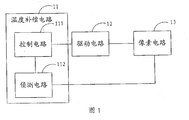
- FIG. 1 is a schematic structural view of a display panel according to an embodiment of the present invention.
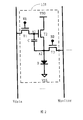
- FIG. 2 is a circuit schematic diagram of a pixel driving circuit in the display panel shown in FIG. 1;
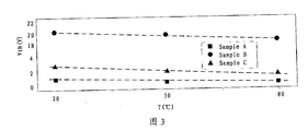
- FIG. 3 is a graph showing a relationship between a threshold voltage of a switching transistor and a temperature in a pixel circuit
- FIG. 5 is a flow chart of a temperature compensation method applied to a display panel according to an embodiment of the present invention.
- the display panel includes a temperature compensation circuit 11, a driving circuit 12, and a pixel circuit 13, wherein the temperature compensation circuit 11 includes a control circuit 111 and a detection circuit 112.
- the control circuit 111, the driving circuit 12, and the pixel circuit 13 are electrically coupled in sequence, and the detecting circuit 112
- the control circuit 111 and the pixel circuit 13 are electrically coupled to each other.
- FIG. 2 is a circuit schematic diagram of a pixel driving circuit in the display panel shown in FIG. 1.
- the pixel circuit 13 includes a plurality of sub-pixel driving circuits 131 arranged in an array, and each of the sub-pixel driving circuits 131 includes a first switching transistor T1, a second switching transistor T2, a third switching transistor T3, and a storage capacitor C. And an organic light emitting diode D.
- the gate of the first switch T1 is electrically connected to the first control signal line WR, the source is electrically connected to the data signal line Vdata, the drain is electrically connected to the first node A1, and the gate of the second switch T2 is electrically connected.
- the first node A1 is connected, the source is electrically connected to the second node A2, and the drain is electrically connected to the positive voltage VDD;
- the gate of the third switch T3 is electrically connected to the second control signal line RD, and the source is electrically connected.
- the first control signal line WR, the data signal line Vdata, and the second control signal line RD are electrically connected to the driving circuit 12, and the detecting signal line Monitor is electrically connected to the detecting circuit 112.
- the control circuit 111, the detection circuit 112, and the drive circuit 12 are circuit modules in an existing timing controller (Timer Control, TCON).
- TCON Timer Control
- the timing controller is mainly composed of a timing generator, a display memory and a management circuit, and a control circuit, and uses an existing timing controller to implement temperature compensation without adding additional hardware costs.
- the detecting circuit 112 is configured to obtain the current threshold voltage Vth of the switching transistor in the pixel circuit 13. Specifically, the detecting circuit 112 acquires the current threshold voltage Vth of the driving switch tube, that is, the second switching tube T2, in each of the sub-pixel driving circuits 131 in the pixel circuit 13 in real time through the detecting signal line Monitor.
- the first switching transistor T1 and the third switching transistor T3 are simultaneously turned on, the data voltage signal applied to the data signal line Vdata and the reference voltage signal applied to the detection signal line Monitor are respectively written into the storage capacitor C.
- the second switching transistor T2 is turned on.
- the reference voltage signal is disconnected, and the current is charged to the parasitic capacitance of the detection signal line Monitor through the third switch tube T3.
- the detection circuit 112 Reading the voltage on the detection signal line Monitor is the current threshold voltage Vth of the driving switch.
- the control circuit 111 is configured to obtain a current voltage difference ⁇ Vth between the current threshold voltage Vth and the initial threshold voltage Vth0, and obtain a current compensation gain G matching the current voltage difference ⁇ Vth in the associated data of the preset voltage difference ⁇ Vth and the compensation gain G.
- the pixel circuit 13 is driven by the current compensation gain G control drive circuit 12 to compensate for the influence of the temperature change on the pixel circuit 13.
- the associated data of the preset voltage difference and the compensation gain is obtained by experimentally obtaining the relationship between the threshold voltage and the temperature of the switching transistor in the pixel circuit 13, the mobility and the temperature, and establishing the temperature, voltage difference and compensation.
- the associated data of the gain, wherein the compensation gain is obtained by a combination of threshold voltage, mobility, and temperature.
- FIG. 3 is a graph showing the relationship between the threshold voltage and the temperature of the switching transistor in the pixel circuit.
- the horizontal axis T represents temperature
- the vertical axis Vth represents a threshold voltage
- the switch tubes are a switch tube Sample A, a switch tube Sample B, and a switch tube Sample C.
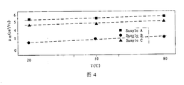
- FIG. 4 is a graph showing the relationship between the mobility of the switching transistor and the temperature in the pixel circuit.
- the horizontal axis T represents temperature
- the vertical axis ⁇ FE represents mobility
- the switch tubes are the switch tube Sample A, the switch tube Sample B, and the switch tube Sample C.
- the variation of the threshold voltage of the switching tube at different operating temperatures that is, the voltage difference, can be estimated.
- the control circuit 111 further determines whether the current voltage difference ⁇ Vth is less than zero, if and only if the current voltage difference ⁇ Vth is less than zero, A compensation gain G matching the current voltage difference ⁇ Vth is obtained in the correlation data of the set voltage difference ⁇ Vth and the compensation gain G.
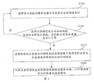
- FIG. 5 is a flow chart of a temperature compensation method applied to a display panel according to an embodiment of the present invention. It should be noted that if there are substantially the same results, the method of the present invention is not limited to the sequence of processes shown in FIG. As shown in FIG. 5, the method includes the steps of:
- Step S101 Obtain a current threshold voltage of the switch tube in the pixel circuit of the display panel.
- the pixel circuit includes a plurality of sub-pixel driving circuits arranged in an array, wherein each sub-pixel driving circuit is configured to drive a corresponding organic light emitting diode in the display panel, and each sub-pixel driving circuit includes driving for driving Corresponding switch tube of organic light emitting diode.
- the current threshold voltage of the switch tube in the pixel circuit of the display panel is obtained, that is, the current threshold voltage of the switch tube for driving each organic light emitting diode in the display panel is obtained respectively.
- Step S102 Obtain a current voltage difference between the current threshold voltage and the initial threshold voltage, and determine whether the current voltage difference is less than zero. If yes, go to step S103, otherwise go to step S101.
- step S102 when the current voltage difference is less than zero, it indicates that the temperature of the switch tube driving the organic light emitting diode is rising, and temperature compensation is needed at this time; otherwise, when the current voltage difference is greater than or equal to zero, the driving is indicated.
- the temperature of the switching tube of the organic light emitting diode is decreasing or remaining unchanged, and no temperature compensation is required at this time.
- the pixel circuit includes a plurality of sub-pixel driving circuits arranged in an array, three different cases may occur: the current voltage difference of the switching transistors in all the sub-pixel driving circuits in the pixel circuit The values are all less than zero, or the current voltage difference of the switching tubes in all the sub-pixel driving circuits in the pixel circuit is greater than or equal to zero, or the current voltage difference of the switching tubes in the partial sub-pixel driving circuits in the pixel circuit is less than zero. The current voltage difference of the switching tubes in the remaining sub-pixel driving circuits is greater than or equal to zero.
- the display panel All of the switching tubes for driving the organic light emitting diodes are temperature-compensated, and it is not necessary to temperature-compensate the switching tubes of the driving organic light-emitting diodes in the display panel, and temperature compensation is performed on the switching tubes of the partial driving organic light-emitting diodes in the display panel and remaining
- the switch tube that drives the OLED does not require temperature compensation.
- Step S103 Obtain a matching current voltage difference value in the associated data of the preset voltage difference value and the compensation gain to obtain a corresponding compensation gain.
- step S103 the associated data of the preset voltage difference and the compensation gain is obtained by: obtaining the relationship between the threshold voltage and the temperature of the switching tube in the pixel circuit, the mobility and the temperature, and establishing the temperature and voltage difference and The associated data of the compensation gain, wherein the compensation gain is obtained by combining the relationship between the threshold voltage, the mobility, and the temperature.
- Step S104 The driving circuit is driven by the current compensation gain control driving circuit to compensate for the influence of the temperature change on the pixel circuit.
- step S104 since the magnitude of the driving current of the driving sub-pixel is related to the data signal voltage, the characteristic of the driving current can be adjusted by using this feature, thereby achieving the technical effect of compensating for the influence of the temperature variation on the pixel circuit.
- the step of driving the pixel circuit by using the current compensation gain control driving circuit is specifically: reducing the data signal voltage according to the current compensation gain, which will be lowered.
- the data signal voltage is applied to the gate of the first switching transistor T1 in the corresponding sub-pixel driving circuit.
- the gate voltage of the second switching transistor T2 is made low. Since the gate voltage of the second switching transistor becomes lower, the driving current for driving the organic light emitting diode D generated by the second switching transistor T2 is reduced, thereby achieving temperature compensation.
- the invention has the beneficial effects that the temperature compensation circuit, the method and the display panel applied to the display panel of the present invention further obtain the current voltage difference between the current threshold voltage and the initial threshold voltage by obtaining the current threshold voltage of the switch tube in the pixel circuit. Obtaining a current compensation gain matching the current voltage difference in the associated data of the preset voltage difference and the compensation gain, and controlling the driving circuit by using the current compensation gain Drive the pixel circuit.
- the present invention can realize temperature compensation of the display panel without an additional temperature sensor, thereby extending the service life of the display panel.
- the invention can realize temperature compensation for the switch tubes of the single driving organic light emitting diodes in the display panel, thereby improving the precision of the temperature compensation and the compensation effect is better.
Landscapes
- Engineering & Computer Science (AREA)
- Physics & Mathematics (AREA)
- Computer Hardware Design (AREA)
- General Physics & Mathematics (AREA)
- Theoretical Computer Science (AREA)
- Control Of Indicators Other Than Cathode Ray Tubes (AREA)
- Electroluminescent Light Sources (AREA)
- Control Of El Displays (AREA)
Abstract
公开了一种应用于显示面板的温度补偿电路、方法及显示面板。该显示面板包括:控制电路(111)、驱动电路(12)、侦测电路(112)以及像素电路(13);其中,侦测电路(112)用于获得像素电路(13)中开关管的当前阈值电压,控制电路(111)获得当前阈值电压与初始阈值电压的当前电压差值,在预设的电压差值与补偿增益的关联数据中获得匹配当前电压差值的当前补偿增益,利用当前补偿增益控制驱动电路驱动像素电路(13)。通过上述方式,不需要额外的温度传感器即可实现显示面板的温度补偿,从而延长显示面板的使用寿命。
Description
本发明涉及有机发光二极管显示领域,特别是涉及一种应用于显示面板的温度补偿电路、方法及显示面板。
有机发光二极管(Organic Light Emitting Diode,OLED)面板相对于液晶显示面板具有反应时间快、重量轻、无视角限制、高对比度等优点,因而成为近年来显示面板的主要研究焦点之一。依有机发光二极管的驱动方式,大致上可分为无源有机发光二极管(PMOLED)面板与有源有机发光二极管AMOLED)面板。其中,AMOLED面板适用于高分辨率与大尺寸的显示面板。
AMOLED面板的像素亮度正比于有机发光二极管的导通电流,而此导通电流的大小是由开关管决定。在实际使用的过程中,随着AMOLED面板温度升高,开关管的阈值电压会逐渐降低,开关管用于驱动有机发光二极管的驱动电流增大,从而使得流经有机发光二极管的导通电流增大。然而AMOLED面板含有大量的有机材料,在高温、高电流的情形下,易使得AMOLED面板加速劣化,从而缩短AMOLED面板的使用寿命。
为了解决上述技术问题,现有技术的做法是:在AMOLED面板上设置温度传感器,通过温度传感器检测AMOLED面板工作时的工作温度并将该温度值反馈给控制电路,控制电路通过统一减少开关管的驱动电流来减少流经有机发光二极管的导通电流,达到实现对AMOLED面板的温度补偿进而延长AMOLED面板的使用寿命的目的。
但是,现有技术的温度补偿中需要增加额外的温度传感器,从而提高了显示面板的生产成本。
【发明内容】
本发明主要解决的技术问题是提供一种应用于显示面板的温度补偿电路、方法及显示面板,不需要额外的温度传感器即可实现显示面板的温度补偿,从而达到延长显示面板的使用寿命的目的。
为解决上述技术问题,本发明采用的一个技术方案是:提供一种应用于显示面板的温度补偿电路,包括:电性耦接的控制电路和侦测电路;其中,控制电路用于电性耦接显示面板的驱动电路,侦测电路用于电性耦接显示面板的像素电路,以获得像素电路中开关管的当前阈值电压,控制电路进一步获得当前阈值电压与初始阈值电压的当前电压差值,在预设的电压差值与补偿增益的关联数据中获得匹配当前电压差值的当前补偿增益,利用当前补偿增益控制驱动电路驱动像素电路,以补偿温度变化对像素电路的影响;其中,控制电路获得当前阈值电压与初始阈值电压的当前电压差值后,进一步判断当前电压差值是否小于零,当且仅当当前电压差值小于零时,在预设的电压差值与补偿增益的关联数据中获得匹配当前电压差值的当前补偿增益;其中,预设的电压差值与补偿增益的关联数据通过以下方式获得:通过实验得到像素电路中开关管的阈值电压与温度关系、迁移率与温度关系,建立温度、电压差值与补偿增益的关联数据,其中补偿增益通过阈值电压、迁移率与温度的关系综合得到。
为解决上述技术问题,本发明采用的另一个技术方案是:提供一种显示面板,包括:控制电路、驱动电路、侦测电路以及像素电路;其中,控制电路、驱动电路以及像素电路依序电性耦接,侦测电路与控制电路、像素电路分别电性耦接,用于获得像素电路中开关管的当前阈值电压,控制电路获得当前阈值电压与初始阈值电压的当前电压差值,在预设的电压差值与补偿增益的关联数据中获得匹配当前电压差值的当前补偿增益,利用当前补偿增益控制驱动电路驱动像素电路,以补偿温度变化对像素电路的影响。为解决上述技术问题,本发明采用的再一个技术方案是:提供一种应用于显示面板的温度补偿方法,包括:获得显示面板的像素电路中开关管的当前阈值电压;获得当前阈值电压与
初始阈值电压的当前电压差值;在预设的电压差值与补偿增益的关联数据中获得匹配当前电压差值的当前补偿增益;利用当前补偿增益控制驱动电路驱动像素电路,以补偿温度变化对像素电路的影响。
本发明的有益效果是:本发明的应用于显示面板的温度补偿电路、方法及显示面板通过获得像素电路中开关管的当前阈值电压后,进一步获得当前阈值电压与初始阈值电压的当前电压差值,在预设的电压差值与补偿增益的关联数据中获得匹配当前电压差值的当前补偿增益,利用当前补偿增益控制驱动电路驱动像素电路。通过上述方式,本发明不需要额外的温度传感器即可实现显示面板的温度补偿,从而延长显示面板的使用寿命。
图1是本发明实施例的显示面板的结构示意图;
图2是图1所示显示面板中像素驱动电路的电路原理图;
图3是像素电路中开关管的阈值电压与温度的关系曲线图;
图4是像素电路中开关管的迁移率与温度的关系曲线图;
图5是本发明实施例的应用于显示面板的温度补偿方法的流程图。
在说明书及权利要求书当中使用了某些词汇来指称特定的组件,所属领域中的技术人员应可理解,制造商可能会用不同的名词来称呼同样的组件。本说明书及权利要求书并不以名称的差异来作为区分组件的方式,而是以组件在功能上的差异来作为区分的基准。下面结合附图和实施例对本发明进行详细说明。
图1是本发明实施例的显示面板的结构示意图。如图1所示,显示面板包括温度补偿电路11、驱动电路12和像素电路13,其中,温度补偿电路11包括控制电路111和侦测电路112。
控制电路111、驱动电路12以及像素电路13依序电性耦接,侦测电路112
与控制电路111、像素电路13分别电性耦接。
具体来说,请一并参考图2,图2是图1所示显示面板中像素驱动电路的电路原理图。如图2所示,像素电路13包括呈阵列排布的多个子像素驱动电路131,每个子像素驱动电路131包括第一开关管T1、第二开关管T2、第三开关管T3、存储电容C、以及有机发光二极管D。
其中,第一开关管T1的栅极电性连接第一控制信号线WR,源极电性连接数据信号线Vdata,漏极电性连接第一节点A1;第二开关管T2的栅极电性连接第一节点A1,源极电性连接第二节点A2,漏极电性连接电源正电压VDD;第三开关管T3的栅极电性连接第二控制信号线RD,源极电性连接第二节点A2,漏极电性连接侦测信号线Monitor;存储电容C的一端电性连接第一节点A1,另一端电性连接第二节点A2;有机发光二极管D的阳极电性连接第二节点A2,有机发光二极管D的阴极电性连接电源负电压Vss。
其中,第一控制信号线WR、数据信号线Vdata、及第二控制信号线RD分别与驱动电路12电性连接,侦测信号线Monitor与侦测电路112电性连接。
其中,控制电路111、侦测电路112和驱动电路12为已有的时序控制器(Timer Control,TCON)中的电路模块。本领域的技术人员可以理解,时序控制器主要由时序发生器、显示存储器及管理电路、控制电路组成,使用已有的时序控制器来实现温度补偿功能,不需要增加额外的硬件费用。
侦测电路112用于获得像素电路13中开关管的当前阈值电压Vth。具体来说,侦测电路112通过侦测信号线Monitor实时获取像素电路13中每个子像素驱动电路131中驱动开关管也即第二开关管T2的当前阈值电压Vth。
具体来说,当第一开关管T1和第三开关管T3同时导通时,施加在数据信号线Vdata上数据电压信号和施加在侦测信号线Monitor的参考电压信号分别写入存储电容C的两端,此时,第二开关管T2导通。接着,断开参考电压信号,电流通过第三开关管T3给侦测信号线Monitor的寄生电容充电,充电到存储电容C两端的压差为当前阈值电压Vth时,第二开关管T2关闭。此时,侦测电路
112读取侦测信号线Monitor上的电压即为驱动开关管的当前阈值电压Vth。
控制电路111用于获得当前阈值电压Vth与初始阈值电压Vth0的当前电压差值ΔVth,在预设的电压差值ΔVth与补偿增益G的关联数据中获得匹配当前电压差值ΔVth的当前补偿增益G,利用当前补偿增益G控制驱动电路12驱动像素电路13,以补偿温度变化对像素电路13的影响。
优选地,预设的电压差值与补偿增益的关联数据通过以下方式获得:通过实验得到像素电路13中开关管的阈值电压与温度关系、迁移率与温度关系,建立温度、电压差值与补偿增益的关联数据,其中补偿增益通过阈值电压、迁移率与温度的关系综合得到。
请一并参考图3,图3是像素电路中开关管的阈值电压与温度的关系曲线图。如图3所示,横轴T代表温度、纵轴Vth代表阈值电压,开关管分别为开关管Sample A、开关管Sample B和开关管Sample C。
从图3可以看出,随着温度T的升高,开关管SampleA、开关管Sample B和开关管Sample C的阈值电压Vth均呈下降趋势。
请一并参考图4,图4是像素电路中开关管的迁移率与温度的关系曲线图。如图4所示,横轴T代表温度、纵轴μFE代表迁移率,开关管分别为开关管Sample A、开关管Sample B和开关管Sample C。
从图3可以看出,随着温度T的升高,开关管SampleA、开关管Sample B和开关管Sample C的迁移率μFE均呈上升趋势。
其中,通过实验测得像素电路中开关管的阈值电压与温度的关系曲线图、迁移率与温度的关系曲线图后,可以估算出不同工作温度下开关管的阈值电压的变化量也即电压差值和补偿增益之间的对应关系并形成查找表。
优选地,控制电路111获得当前阈值电压Vth与初始阈值电压Vth0的当前电压差值ΔVth后,进一步判断当前电压差值ΔVth是否小于零,当且仅当当前电压差值ΔVth小于零时,在预设的电压差值ΔVth与补偿增益G的关联数据中获得匹配当前电压差值ΔVth的补偿增益G。
本领域的技术人员可以理解,当当前电压差值ΔVth小于零时,则说明像素电路13中开关管的温度在上升,也即此时需要进行温度补偿;反之,当当前电压差值ΔVth大于或等于零时,则说明书像素电路13中的开关管的温度在下降或保持不变,也即此时不需要进行温度补偿。
图5是本发明实施例的应用于显示面板的温度补偿方法的流程图。需注意的是,若有实质上相同的结果,本发明的方法并不以图5所示的流程顺序为限。如图5所示,该方法包括步骤:
步骤S101:获得显示面板的像素电路中开关管的当前阈值电压。
在步骤S101中,像素电路包括呈阵列排布的多个子像素驱动电路,其中,每一子像素驱动电路用于驱动显示面板中对应的有机发光二极管,每一子像素驱动电路中包括用于驱动对应的有机发光二极管的开关管。
其中,获得显示面板的像素电路中开关管的当前阈值电压也即为分别获得显示面板中驱动各有机发光二极管的开关管的当前阈值电压。
步骤S102:获得当前阈值电压与初始阈值电压的当前电压差值,并判断当前电压差值是否小于零,若是,执行步骤S103,否则执行步骤S101。
在步骤S102中,当当前电压差值小于零时,则说明驱动有机发光二极管的开关管的温度在上升,此时需要进行温度补偿;反之,当当前电压差值大于或等于零时,则说明驱动有机发光二极管的开关管的温度在下降或保持不变,此时不需要进行温度补偿。
本领域的技术人员可以理解,由于像素电路包括呈阵列排布的多个子像素驱动电路,因此,会出现三种不同的情况:像素电路中的所有子像素驱动电路中的开关管的当前电压差值均小于零、或者像素电路中的所有子像素驱动电路中的开关管的当前电压差值均大于等于零、或者像素电路中的部分子像素驱动电路中的开关管的当前电压差值小于零而剩余的子像素驱动电路中的开关管的当前电压差值大于等于零。
换个角度来说,在进行温度补偿时,会出现三种不同的情况:对显示面板
中的所有驱动有机发光二极管的开关管进行温度补偿、不需要对显示面板中的驱动有机发光二极管的开关管进行温度补偿、对显示面板中的部分驱动有机发光二极管的开关管进行温度补偿且剩余的驱动有机发光二极管的开关管不需要进行温度补偿。
步骤S103:在预设的电压差值与补偿增益的关联数据中获得匹配当前电压差值进而得到对应的补偿增益。
在步骤S103中,预设的电压差值与补偿增益的关联数据通过以下方式获得:通过实验得到像素电路中开关管的阈值电压与温度关系、迁移率与温度关系,建立温度、电压差值与补偿增益的关联数据,其中补偿增益通过阈值电压、迁移率与温度的关系综合得到。
步骤S104:利用当前补偿增益控制驱动电路驱动像素电路,以补偿温度变化对像素电路的影响。
在步骤S104中,由于驱动子像素的驱动电流的大小与数据信号电压相关,因此,可以利用此特点来调整驱动电流的大小,以此达到补偿温度变化对像素电路的影响的技术效果。
以图2所示的电路原理图为例,当通过数据信号电压调整驱动电流时,利用当前补偿增益控制驱动电路驱动像素电路的步骤具体为:根据当前补偿增益降低数据信号电压,将降低后的数据信号电压施加至对应的子像素驱动电路中第一开关管T1的栅极。其中,由于第一开关管T1的栅极的数据信号电压降低,当第一开关管T1被打开时,使得第二开关管T2的栅极电压变低。由于第二开关管的栅极电压变低,所以第二开关管T2产生的驱动有机发光二极管D的驱动电流减小,从而实现温度补偿。
本发明的有益效果是:本发明的应用于显示面板的温度补偿电路、方法和显示面板通过获得像素电路中开关管的当前阈值电压后,进一步获得当前阈值电压与初始阈值电压的当前电压差值,在预设的电压差值与补偿增益的关联数据中获得匹配当前电压差值的当前补偿增益,利用当前补偿增益控制驱动电路
驱动像素电路。通过上述方式,本发明不需要额外的温度传感器即可实现显示面板的温度补偿,从而延长显示面板的使用寿命。另外,本发明可以实现对显示面板中的单个驱动有机发光二极管的开关管分别进行温度补偿,从而提高了温度补偿的精度,补偿效果更好。
以上所述仅为本发明的实施方式,并非因此限制本发明的专利范围,凡是利用本发明说明书及附图内容所作的等效结构或等效流程变换,或直接或间接运用在其他相关的技术领域,均同理包括在本发明的专利保护范围内。
Claims (10)
- 一种应用于显示面板的温度补偿电路,其中,包括:电性耦接的控制电路和侦测电路;其中,所述控制电路用于电性耦接所述显示面板的驱动电路,所述侦测电路用于电性耦接所述显示面板的像素电路,以获得所述像素电路中开关管的当前阈值电压,所述控制电路进一步获得所述当前阈值电压与初始阈值电压的当前电压差值,在预设的电压差值与补偿增益的关联数据中获得匹配所述当前电压差值的当前补偿增益,利用所述当前补偿增益控制所述驱动电路驱动所述像素电路,以补偿温度变化对所述像素电路的影响;其中,所述控制电路获得所述当前阈值电压与初始阈值电压的当前电压差值后,进一步判断所述当前电压差值是否小于零,当且仅当所述当前电压差值小于零时,在预设的电压差值与补偿增益的关联数据中获得匹配所述当前电压差值的当前补偿增益;其中,所述预设的电压差值与补偿增益的关联数据通过以下方式获得:通过实验得到所述像素电路中开关管的阈值电压与温度关系、迁移率与温度关系,建立所述温度、所述电压差值与所述补偿增益的关联数据,其中所述补偿增益通过所述阈值电压、所述迁移率与所述温度的关系综合得到。
- 一种显示面板,其中,包括:控制电路、驱动电路、侦测电路以及像素电路;其中,所述控制电路、所述驱动电路以及所述像素电路依序电性耦接,所述侦测电路与所述控制电路、所述像素电路分别电性耦接,用于获得所述像素电路中开关管的当前阈值电压,所述控制电路获得所述当前阈值电压与初始阈值电压的当前电压差值,在预设的电压差值与补偿增益的关联数据中获得匹配所述当前电压差值的当前补偿增益,利用所述当前补偿增益控制所述驱动电路驱动所述像素电路,以补偿温度变化对所述像素电路的影响。
- 根据权利要求2所述的显示面板,其中,所述控制电路获得所述当前阈值电压与初始阈值电压的当前电压差值后,进一步判断所述当前电压差值是否小于零,当且仅当所述当前电压差值小于零时,在预设的电压差值与补偿增益的关联数据中获得匹配所述当前电压差值的当前补偿增益。
- 根据权利要求2所述的显示面板,其中,所述预设的电压差值与补偿增益的关联数据通过以下方式获得:通过实验得到所述像素电路中开关管的阈值电压与温度关系、迁移率与温度关系,建立所述温度、所述电压差值与所述补偿增益的关联数据,其中所述补偿增益通过所述阈值电压、所述迁移率与所述温度的关系综合得到。
- 根据权利要求2所述的显示面板,其中,所述像素电路包括呈阵列排布的多个子像素驱动电路,每一所述子像素驱动电路包括第一开关管、第二开关管、第三开关管、存储电容和有机发光二极管;其中,所述第一开关管的栅极电性连接第一控制信号线,源极电性连接数据信号线,漏极电性连接第一节点;所述第二开关管的栅极电性连接所述第一节点,源极电性连接第二节点,漏极电性连接电源正电压;所述第三开关管的栅极电性连接第二控制信号线,源极电性连接所述第二节点,漏极电性连接侦测信号线;所述存储电容的一端电性连接所述第一节点,另一端电性连接所述第二节点;所述机发光二极管的阳极电性连接所述第二节点,所述有机发光二极管的阴极电性连接电源负电压;其中,所述第一控制信号线、所述数据信号线和所述第二控制信号线分别与所述驱动电路电性连接,所述侦测信号线与所述侦测电路电性连接。
- 根据权利要求3所述的显示面板,其中,所述像素电路包括呈阵列排布的多个子像素驱动电路,每一所述子像素驱动电路包括第一开关管、第二开关管、第三开关管、存储电容和有机发光二极 管;其中,所述第一开关管的栅极电性连接第一控制信号线,源极电性连接数据信号线,漏极电性连接第一节点;所述第二开关管的栅极电性连接所述第一节点,源极电性连接第二节点,漏极电性连接电源正电压;所述第三开关管的栅极电性连接第二控制信号线,源极电性连接所述第二节点,漏极电性连接侦测信号线;所述存储电容的一端电性连接所述第一节点,另一端电性连接所述第二节点;所述机发光二极管的阳极电性连接所述第二节点,所述有机发光二极管的阴极电性连接电源负电压;其中,所述第一控制信号线、所述数据信号线和所述第二控制信号线分别与所述驱动电路电性连接,所述侦测信号线与所述侦测电路电性连接。
- 根据权利要求4所述的显示面板,其中,所述像素电路包括呈阵列排布的多个子像素驱动电路,每一所述子像素驱动电路包括第一开关管、第二开关管、第三开关管、存储电容和有机发光二极管;其中,所述第一开关管的栅极电性连接第一控制信号线,源极电性连接数据信号线,漏极电性连接第一节点;所述第二开关管的栅极电性连接所述第一节点,源极电性连接第二节点,漏极电性连接电源正电压;所述第三开关管的栅极电性连接第二控制信号线,源极电性连接所述第二节点,漏极电性连接侦测信号线;所述存储电容的一端电性连接所述第一节点,另一端电性连接所述第二节点;所述机发光二极管的阳极电性连接所述第二节点,所述有机发光二极管的阴极电性连接电源负电压;其中,所述第一控制信号线、所述数据信号线和所述第二控制信号线分别与所述驱动电路电性连接,所述侦测信号线与所述侦测电路电性连接。
- 一种应用于显示面板的温度补偿方法,其中,包括:获得所述显示面板的像素电路中开关管的当前阈值电压;获得所述当前阈值电压与初始阈值电压的当前电压差值;在预设的电压差值与补偿增益的关联数据中获得匹配所述当前电压差值的当前补偿增益;利用所述当前补偿增益控制所述驱动电路驱动所述像素电路,以补偿温度变化对所述像素电路的影响。
- 根据权利要求8所述的方法,其中,所述获得所述当前阈值电压与初始阈值电压的当前电压差值后,所述方法进一步包括:判断所述当前电压差值是否小于零,当且仅当所述当前电压差值小于零时,在预设的电压差值与补偿增益的关联数据中获得匹配所述当前电压差值的当前补偿增益。
- 根据权利要求8所述的方法,其中,所述预设的电压差值与补偿增益的关联数据通过以下方式获得:通过实验得到所述像素电路中开关管的阈值电压与温度关系、迁移率与温度关系,建立所述温度、所述电压差值与所述补偿增益的关联数据,其中所述补偿增益通过所述阈值电压、所述迁移率与所述温度的关系综合得到。
Priority Applications (1)
| Application Number | Priority Date | Filing Date | Title |
|---|---|---|---|
| US15/742,232 US10388226B2 (en) | 2017-10-11 | 2017-11-23 | Temperature compensation circuit and method for a display panel and display panel |
Applications Claiming Priority (2)
| Application Number | Priority Date | Filing Date | Title |
|---|---|---|---|
| CN201710949708.5A CN107731160B (zh) | 2017-10-11 | 2017-10-11 | 一种应用于显示面板的温度补偿电路、方法及显示面板 |
| CN201710949708.5 | 2017-10-11 |
Publications (1)
| Publication Number | Publication Date |
|---|---|
| WO2019071735A1 true WO2019071735A1 (zh) | 2019-04-18 |
Family
ID=61210804
Family Applications (1)
| Application Number | Title | Priority Date | Filing Date |
|---|---|---|---|
| PCT/CN2017/112475 Ceased WO2019071735A1 (zh) | 2017-10-11 | 2017-11-23 | 一种应用于显示面板的温度补偿电路、方法及显示面板 |
Country Status (2)
| Country | Link |
|---|---|
| CN (1) | CN107731160B (zh) |
| WO (1) | WO2019071735A1 (zh) |
Families Citing this family (14)
| Publication number | Priority date | Publication date | Assignee | Title |
|---|---|---|---|---|
| US10748478B2 (en) | 2018-06-11 | 2020-08-18 | Shenzhen China Star Optoelectronics Semiconductor Display Technology Co., Ltd. | OLED panel temperature compensation system and OLED panel temperature compensation method |
| CN108831380A (zh) * | 2018-06-11 | 2018-11-16 | 深圳市华星光电半导体显示技术有限公司 | Oled面板温度补偿系统及oled面板温度补偿方法 |
| CN109036268B (zh) * | 2018-07-17 | 2020-06-30 | 深圳市华星光电半导体显示技术有限公司 | Oled显示装置的补偿系统及补偿方法 |
| CN109119025B (zh) * | 2018-09-28 | 2021-04-06 | 京东方科技集团股份有限公司 | 电压补偿方法及装置、显示面板 |
| CN109473065B (zh) * | 2018-11-19 | 2020-08-14 | 合肥鑫晟光电科技有限公司 | 显示控制方法、装置及显示面板 |
| CN109377958B (zh) * | 2018-12-04 | 2020-04-28 | 深圳市华星光电半导体显示技术有限公司 | 基于温度补偿的栅极驱动电路及显示器 |
| CN109377931B (zh) * | 2018-12-07 | 2022-02-08 | 合肥鑫晟光电科技有限公司 | 阈值电压获取方法、像素补偿方法及显示面板 |
| CN109493805B (zh) * | 2018-12-12 | 2021-04-27 | 合肥鑫晟光电科技有限公司 | 一种显示面板的补偿方法和装置 |
| CN109727578A (zh) | 2018-12-14 | 2019-05-07 | 合肥鑫晟光电科技有限公司 | 显示装置的补偿方法、装置和显示设备 |
| CN110660358B (zh) * | 2019-09-17 | 2021-09-14 | 昆山龙腾光电股份有限公司 | 显示装置及其驱动补偿方法 |
| CN112233627B (zh) * | 2020-12-14 | 2021-04-20 | 北京显芯科技有限公司 | 背光电路的控制方法、背光电路以及lcd显示屏 |
| CN113707093B (zh) * | 2021-08-18 | 2023-04-07 | 深圳市华星光电半导体显示技术有限公司 | 显示像素电路结构及显示面板 |
| CN114755858A (zh) * | 2022-03-29 | 2022-07-15 | 咸阳博凯樾电子科技有限公司 | 一种led背光面板及led面板 |
| CN120564597A (zh) * | 2024-02-29 | 2025-08-29 | 华为技术有限公司 | 显示面板及电子设备 |
Citations (5)
| Publication number | Priority date | Publication date | Assignee | Title |
|---|---|---|---|---|
| CN103903559A (zh) * | 2012-12-24 | 2014-07-02 | 乐金显示有限公司 | 有机发光显示装置和驱动有机发光显示装置的方法 |
| CN104700772A (zh) * | 2013-12-03 | 2015-06-10 | 乐金显示有限公司 | 有机发光显示装置及其图像质量补偿方法 |
| CN105575332A (zh) * | 2014-10-31 | 2016-05-11 | 乐金显示有限公司 | 有机发光二极管显示装置及其驱动方法 |
| CN106935192A (zh) * | 2017-05-12 | 2017-07-07 | 京东方科技集团股份有限公司 | 像素电路及其驱动方法、显示装置 |
| CN106991969A (zh) * | 2017-06-09 | 2017-07-28 | 京东方科技集团股份有限公司 | 显示面板、像素的补偿电路和补偿方法 |
Family Cites Families (11)
| Publication number | Priority date | Publication date | Assignee | Title |
|---|---|---|---|---|
| JP2000294154A (ja) * | 1999-04-12 | 2000-10-20 | Hitachi Ltd | プラズマディスプレイ装置 |
| KR20010039316A (ko) * | 1999-10-29 | 2001-05-15 | 김영남 | 평판디스플레이의 전류보상 장치 |
| JP4154828B2 (ja) * | 2000-02-17 | 2008-09-24 | コニカミノルタホールディングス株式会社 | 液晶表示素子の駆動方法及び液晶表示装置 |
| CN1394026A (zh) * | 2001-07-02 | 2003-01-29 | 福建华科光电有限公司 | 一种新颖的interleaver温度补偿方法 |
| US9014399B2 (en) * | 2011-03-11 | 2015-04-21 | Fairchild Semiconductor Corporation | ECM digital microphone temperature compensation |
| CN102654973B (zh) * | 2011-08-15 | 2014-11-19 | 京东方科技集团股份有限公司 | 像素电路及其驱动方法、显示面板 |
| JP2013076811A (ja) * | 2011-09-30 | 2013-04-25 | Sony Corp | 画素回路、画素回路の駆動方法、表示装置、および、電子機器 |
| TWI467540B (zh) * | 2012-12-14 | 2015-01-01 | Upi Semiconductor Corp | 閘極驅動電路之參考電壓產生器及參考電壓產生方法 |
| CN203100462U (zh) * | 2013-01-11 | 2013-07-31 | 福州伟通机械设备有限公司 | 一种温度补偿装置 |
| CN104180823B (zh) * | 2014-01-10 | 2016-08-17 | 中国商用飞机有限责任公司北京民用飞机技术研究中心 | 一种温度补偿方法及装置 |
| CN106409231B (zh) * | 2016-10-31 | 2018-10-12 | 昆山国显光电有限公司 | 一种亮度补偿方法、装置及显示设备 |
-
2017
- 2017-10-11 CN CN201710949708.5A patent/CN107731160B/zh active Active
- 2017-11-23 WO PCT/CN2017/112475 patent/WO2019071735A1/zh not_active Ceased
Patent Citations (5)
| Publication number | Priority date | Publication date | Assignee | Title |
|---|---|---|---|---|
| CN103903559A (zh) * | 2012-12-24 | 2014-07-02 | 乐金显示有限公司 | 有机发光显示装置和驱动有机发光显示装置的方法 |
| CN104700772A (zh) * | 2013-12-03 | 2015-06-10 | 乐金显示有限公司 | 有机发光显示装置及其图像质量补偿方法 |
| CN105575332A (zh) * | 2014-10-31 | 2016-05-11 | 乐金显示有限公司 | 有机发光二极管显示装置及其驱动方法 |
| CN106935192A (zh) * | 2017-05-12 | 2017-07-07 | 京东方科技集团股份有限公司 | 像素电路及其驱动方法、显示装置 |
| CN106991969A (zh) * | 2017-06-09 | 2017-07-28 | 京东方科技集团股份有限公司 | 显示面板、像素的补偿电路和补偿方法 |
Also Published As
| Publication number | Publication date |
|---|---|
| CN107731160A (zh) | 2018-02-23 |
| CN107731160B (zh) | 2019-08-30 |
Similar Documents
| Publication | Publication Date | Title |
|---|---|---|
| WO2019071735A1 (zh) | 一种应用于显示面板的温度补偿电路、方法及显示面板 | |
| CN107016964B (zh) | 像素电路、其驱动方法和显示装置 | |
| US10388226B2 (en) | Temperature compensation circuit and method for a display panel and display panel | |
| US10297194B2 (en) | Organic light emitting diode display device having a target current setting | |
| CN102651194B (zh) | 电压驱动像素电路及其驱动方法、显示面板 | |
| CN103198794B (zh) | 像素电路及其驱动方法、有机发光显示面板及显示装置 | |
| CN105427809B (zh) | 像素补偿电路及amoled显示装置 | |
| WO2021120315A1 (zh) | 像素混合补偿电路及像素混合补偿方法 | |
| CN108154834B (zh) | 电致发光显示面板及发光器件的跨压检测方法 | |
| WO2019037300A1 (zh) | Amoled像素驱动电路 | |
| WO2019033487A1 (zh) | 用于oled显示设备的像素驱动电路及oled显示设备 | |
| WO2016155177A1 (zh) | 一种检测电路、检测方法和驱动系统 | |
| WO2018223702A1 (zh) | 显示面板、像素的补偿电路和补偿方法 | |
| WO2015192399A1 (zh) | 有机发光二极管的像素驱动电路及像素驱动方法 | |
| WO2015180352A1 (zh) | 像素电路及其驱动方法、有机发光显示面板及显示装置 | |
| TW201618070A (zh) | 像素電路及其驅動方法和有機發光顯示器 | |
| WO2015180278A1 (zh) | 像素电路及其驱动方法、显示装置 | |
| TW201606738A (zh) | 主動式有機發光二極體顯示器的像素電路 | |
| WO2013037295A1 (zh) | Oled像素结构及驱动方法 | |
| WO2016086626A1 (zh) | 一种像素驱动电路、像素驱动方法和显示装置 | |
| US11094253B2 (en) | Pixel driving circuit, method for driving the same, array substrate and display device | |
| WO2021203479A1 (zh) | 像素驱动电路和显示面板 | |
| WO2017020360A1 (zh) | Amoled像素驱动电路及像素驱动方法 | |
| WO2016070477A1 (zh) | 有机发光显示器像素驱动电路 | |
| CN110264957A (zh) | 一种像素电路的补偿方法、装置、显示设备 |
Legal Events
| Date | Code | Title | Description |
|---|---|---|---|
| 121 | Ep: the epo has been informed by wipo that ep was designated in this application |
Ref document number: 17928382 Country of ref document: EP Kind code of ref document: A1 |
|
| NENP | Non-entry into the national phase |
Ref country code: DE |
|
| 122 | Ep: pct application non-entry in european phase |
Ref document number: 17928382 Country of ref document: EP Kind code of ref document: A1 |