WO2019065417A1 - エラストマー製圧電素子、及びエラストマー製圧電素子の製造方法 - Google Patents
エラストマー製圧電素子、及びエラストマー製圧電素子の製造方法 Download PDFInfo
- Publication number
- WO2019065417A1 WO2019065417A1 PCT/JP2018/034660 JP2018034660W WO2019065417A1 WO 2019065417 A1 WO2019065417 A1 WO 2019065417A1 JP 2018034660 W JP2018034660 W JP 2018034660W WO 2019065417 A1 WO2019065417 A1 WO 2019065417A1
- Authority
- WO
- WIPO (PCT)
- Prior art keywords
- dielectric
- elastomer
- electrode
- piezoelectric element
- insulating
- Prior art date
- Legal status (The legal status is an assumption and is not a legal conclusion. Google has not performed a legal analysis and makes no representation as to the accuracy of the status listed.)
- Ceased
Links
Images



Classifications
-
- H—ELECTRICITY
- H10—SEMICONDUCTOR DEVICES; ELECTRIC SOLID-STATE DEVICES NOT OTHERWISE PROVIDED FOR
- H10N—ELECTRIC SOLID-STATE DEVICES NOT OTHERWISE PROVIDED FOR
- H10N30/00—Piezoelectric or electrostrictive devices
- H10N30/50—Piezoelectric or electrostrictive devices having a stacked or multilayer structure
-
- H—ELECTRICITY
- H01—ELECTRIC ELEMENTS
- H01B—CABLES; CONDUCTORS; INSULATORS; SELECTION OF MATERIALS FOR THEIR CONDUCTIVE, INSULATING OR DIELECTRIC PROPERTIES
- H01B17/00—Insulators or insulating bodies characterised by their form
- H01B17/56—Insulating bodies
- H01B17/64—Insulating bodies with conductive admixtures, inserts or layers
-
- H—ELECTRICITY
- H01—ELECTRIC ELEMENTS
- H01B—CABLES; CONDUCTORS; INSULATORS; SELECTION OF MATERIALS FOR THEIR CONDUCTIVE, INSULATING OR DIELECTRIC PROPERTIES
- H01B3/00—Insulators or insulating bodies characterised by the insulating materials; Selection of materials for their insulating or dielectric properties
- H01B3/18—Insulators or insulating bodies characterised by the insulating materials; Selection of materials for their insulating or dielectric properties mainly consisting of organic substances
- H01B3/28—Insulators or insulating bodies characterised by the insulating materials; Selection of materials for their insulating or dielectric properties mainly consisting of organic substances natural or synthetic rubbers
-
- H—ELECTRICITY
- H10—SEMICONDUCTOR DEVICES; ELECTRIC SOLID-STATE DEVICES NOT OTHERWISE PROVIDED FOR
- H10N—ELECTRIC SOLID-STATE DEVICES NOT OTHERWISE PROVIDED FOR
- H10N30/00—Piezoelectric or electrostrictive devices
- H10N30/01—Manufacture or treatment
- H10N30/05—Manufacture of multilayered piezoelectric or electrostrictive devices, or parts thereof, e.g. by stacking piezoelectric bodies and electrodes
-
- H—ELECTRICITY
- H10—SEMICONDUCTOR DEVICES; ELECTRIC SOLID-STATE DEVICES NOT OTHERWISE PROVIDED FOR
- H10N—ELECTRIC SOLID-STATE DEVICES NOT OTHERWISE PROVIDED FOR
- H10N30/00—Piezoelectric or electrostrictive devices
- H10N30/01—Manufacture or treatment
- H10N30/05—Manufacture of multilayered piezoelectric or electrostrictive devices, or parts thereof, e.g. by stacking piezoelectric bodies and electrodes
- H10N30/057—Manufacture of multilayered piezoelectric or electrostrictive devices, or parts thereof, e.g. by stacking piezoelectric bodies and electrodes by stacking bulk piezoelectric or electrostrictive bodies and electrodes
-
- H—ELECTRICITY
- H10—SEMICONDUCTOR DEVICES; ELECTRIC SOLID-STATE DEVICES NOT OTHERWISE PROVIDED FOR
- H10N—ELECTRIC SOLID-STATE DEVICES NOT OTHERWISE PROVIDED FOR
- H10N30/00—Piezoelectric or electrostrictive devices
- H10N30/01—Manufacture or treatment
- H10N30/09—Forming piezoelectric or electrostrictive materials
- H10N30/092—Forming composite materials
-
- H—ELECTRICITY
- H10—SEMICONDUCTOR DEVICES; ELECTRIC SOLID-STATE DEVICES NOT OTHERWISE PROVIDED FOR
- H10N—ELECTRIC SOLID-STATE DEVICES NOT OTHERWISE PROVIDED FOR
- H10N30/00—Piezoelectric or electrostrictive devices
- H10N30/80—Constructional details
- H10N30/85—Piezoelectric or electrostrictive active materials
- H10N30/852—Composite materials, e.g. having 1-3 or 2-2 type connectivity
-
- H—ELECTRICITY
- H10—SEMICONDUCTOR DEVICES; ELECTRIC SOLID-STATE DEVICES NOT OTHERWISE PROVIDED FOR
- H10N—ELECTRIC SOLID-STATE DEVICES NOT OTHERWISE PROVIDED FOR
- H10N30/00—Piezoelectric or electrostrictive devices
- H10N30/80—Constructional details
- H10N30/87—Electrodes or interconnections, e.g. leads or terminals
- H10N30/871—Single-layered electrodes of multilayer piezoelectric or electrostrictive devices, e.g. internal electrodes
-
- H—ELECTRICITY
- H10—SEMICONDUCTOR DEVICES; ELECTRIC SOLID-STATE DEVICES NOT OTHERWISE PROVIDED FOR
- H10N—ELECTRIC SOLID-STATE DEVICES NOT OTHERWISE PROVIDED FOR
- H10N30/00—Piezoelectric or electrostrictive devices
- H10N30/80—Constructional details
- H10N30/87—Electrodes or interconnections, e.g. leads or terminals
- H10N30/877—Conductive materials
- H10N30/878—Conductive materials the principal material being non-metallic, e.g. oxide or carbon based
-
- H—ELECTRICITY
- H10—SEMICONDUCTOR DEVICES; ELECTRIC SOLID-STATE DEVICES NOT OTHERWISE PROVIDED FOR
- H10N—ELECTRIC SOLID-STATE DEVICES NOT OTHERWISE PROVIDED FOR
- H10N30/00—Piezoelectric or electrostrictive devices
- H10N30/80—Constructional details
- H10N30/85—Piezoelectric or electrostrictive active materials
- H10N30/857—Macromolecular compositions
Definitions
- the present invention relates to an elastomeric piezoelectric element and a method of manufacturing an elastomeric piezoelectric element.
- an elastomeric piezoelectric element configured by a plurality of unit layers.
- the plurality of unit layers are disposed along the thickness direction of the elastomeric piezoelectric element.
- Each unit layer includes an elastomeric dielectric portion and an electrode portion provided on the dielectric portion.
- JP 2012-125140 A Japanese Patent Application Publication No. 2016-509826
- an electrode part of a piezoelectric element made of an elastomer for example, a metal deposition electrode part formed by metal deposition or an electrode part made of a conductive elastomer is used.
- the electrode portion made of a conductive elastomer is excellent in the followability to the displacement of the dielectric portion as compared with the metal deposition electrode portion. Therefore, when the electrode part made of a conductive elastomer is used, the durability of the piezoelectric element made of elastomer against repeated displacement operation of the dielectric part can be enhanced.
- the electrode portion made of the conductive elastomer is formed thicker than the metal deposition electrode portion. Therefore, as shown in FIG. 7A, the air layer 23 is easily formed around the electrode portion 22 between the dielectric portions 21 adjacent in the thickness direction (stacking direction). Such an air layer 23 causes dielectric breakdown due to creeping discharge. Further, as a method of removing the air layer 23, it is conceivable to compress in the laminating direction so as to bring the adjacent dielectric portions 21 into contact with each other when manufacturing the elastomeric piezoelectric element. However, in this case, as shown in FIG. 7B, the dielectric portion 21 is partially deformed to fill the air layer around the electrode portion 22 as shown in FIG. A thin spot 21a occurs. As a result, dielectric breakdown is likely to occur at the location 21a.
- An object of the present invention is to improve the durability of an elastomeric piezoelectric element against dielectric breakdown.
- An elastomeric piezoelectric element for solving the above problems comprises a plurality of unit layers disposed along the thickness direction of the elastomeric piezoelectric element, each unit layer being a sheet-like dielectric portion made of dielectric elastomer, An electrode portion made of a conductive elastomer partially disposed on the first surface of the dielectric portion, and a thickness of the unit layer provided on at least a part of the periphery of the electrode portion and where the electrode portion is not disposed And an insulating portion made of insulating elastomer which approaches the thickness of the unit layer in the portion where the electrode portion is disposed.
- the insulating portion made of insulating elastomer is disposed around the electrode portion in the unit layer. Therefore, it is difficult to form a large air layer around the electrode portion. Moreover, even if an air layer is formed around the electrode portion, creeping discharge hardly occurs because the insulating portion serves as a barrier.
- the insulating portion by providing the insulating portion, the difference between the thickness of the unit layer in the portion where the electrode portion is disposed and the thickness of the unit layer in the portion where the electrode portion is not disposed is reduced. That is, the surface of the unit layer on which the electrode portion is disposed is flattened. Therefore, when an external force at the time of compression or the like acts, the shape of the dielectric portion is easily maintained, and a portion where the thickness of the dielectric portion is partially thin hardly occurs between the adjacent electrode portions.
- the insulating portion is preferably made of the same material as the dielectric portion. According to the above configuration, it is possible to reduce the types of materials constituting the elastomeric piezoelectric element.
- the insulating portion be constituted by a projecting portion in which a part of the dielectric portion is protruded to the first surface side. According to the above configuration, there is no interface (bonding surface) between the dielectric portion and the insulating portion. Therefore, it is suppressed that the displacement of a dielectric part is prevented by the said interface.
- the electrode portion contains an insulating polymer and a conductive filler, and the insulating portion contains the same insulating polymer as the insulating polymer contained in the electrode portion. Is preferred.
- a unit layer is formed, and the unit layer is a sheet-like dielectric portion made of dielectric elastomer, and a conductive portion partially disposed on the first surface of the dielectric portion
- the unit made of an elastomer electrode portion and at least a part of the periphery of the electrode portion, where the thickness of the unit layer in the portion where the electrode portion is not disposed is the unit in the portion where the electrode portion is disposed It has a unit layer formation process provided with insulation part made from insulation elastomer which approaches thickness of a layer, and a lamination process which laminates and joins a plurality of the unit layers formed respectively by the unit layer formation process.
- the electrode portion and the insulating portion are preferably formed on the first surface of the dielectric portion.
- the dielectric portion is formed so as to have a protruding portion which protrudes to the first surface side and which constitutes the insulating portion.
- the unit layer thickness in the portion where the electrode portion is disposed and the unit layer in the portion where the electrode portion is not disposed is smaller. That is, the surface of the unit layer on which the electrode portion is disposed is flattened.
- the flattened unit layers are stacked, so that a large air layer is not formed around the electrode portion.
- the presence of the insulating portion suppresses deformation of the dielectric portion toward the electrode portion side, and the thickness of the dielectric portion is partially thin between the adjacent electrode portions. It is less likely to occur.
- the first step of forming the electrode portion on a part of the upper surface of the dielectric portion formed previously, and the upper surface of the dielectric portion formed previously A second step of forming the dielectric portion and the insulating portion by applying and curing a raw material composition of dielectric elastomer to at least a part of the periphery of the electrode portion and the upper surface of the electrode portion .
- the raw material composition of the dielectric elastomer when the raw material composition of the dielectric elastomer is applied in the second step, leveling is performed so that the upper surface of the applied raw material composition approaches horizontal. Therefore, the difference in level between the upper surface of the portion applied to the electrode portion in the applied raw material composition and the upper surface of the portion applied to the dielectric portion is reduced. As a result, it is possible to form a unit layer in which the difference between the thickness of the portion in which the electrode portion is disposed and the thickness of the portion in which the electrode portion is not disposed is small.
- the first step and the second step are repeatedly performed.
- the durability of the elastomeric piezoelectric element against dielectric breakdown can be improved.
- Sectional drawing which shows schematic structure of the piezoelectric element made from an elastomer.
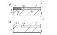
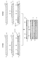
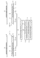
- (A), (b) is a fragmentary sectional view which shows the relationship between a dielectric part, an electrode part, and an insulation part. Explanatory drawing which shows the 1st manufacturing method of an elastomer piezoelectric element. Explanatory drawing which shows the 2nd manufacturing method of elastomer piezoelectric elements. Sectional drawing which shows schematic structure of the elastomer-made piezoelectric element of a modification. Explanatory drawing which shows the lamination process of the example of a change.
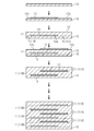
- (A), (b) is sectional drawing of the conventional piezoelectric element made from elastomer. Explanatory drawing which shows the 3rd manufacturing method of an elastomer piezoelectric element.
- (A), (b) is sectional drawing which shows schematic structure of the elastomer-made piezoelectric element of a modification.
- the elastomeric piezoelectric element 10 is a multilayer structure provided with a plurality of unit layers 11 arranged along the thickness direction X of the elastomeric piezoelectric element 10.
- the plurality of unit layers 11 are configured by the plurality of first unit layers 11A and the plurality of second unit layers 11B.
- the first unit layers 11A and the second unit layers 11B are alternately arranged in the thickness direction X.
- the first unit layer 11A is provided with a dielectric portion 12 made of dielectric elastomer in the form of a sheet having a constant thickness.
- the dielectric portion 12 is formed in a thin film shape, and has a thickness of, for example, 20 to 200 ⁇ m.
- the dielectric elastomer (material of the dielectric part 12) which comprises the dielectric part 12 is not specifically limited,
- the dielectric elastomer used for a well-known elastomer piezoelectric element can be used.
- Examples of the dielectric elastomer include polyrotaxane, silicone elastomer, acrylic elastomer, and urethane elastomer. One of these dielectric elastomers may be used, or multiple types may be used in combination.
- An electrode portion 13 made of a conductive elastomer is disposed at a central portion of the first surface 12 a of the dielectric portion 12.
- the electrode portion 13 is formed in a thin film shape, and has a thickness of, for example, 10 to 100 ⁇ m.
- the conductive elastomer (material of the electrode part 13) which comprises the electrode part 13 is not specifically limited,
- the conductive elastomer used for a well-known elastomer piezoelectric element can be used.
- the conductive elastomer containing an insulating polymer and a conductive filler is mentioned, for example.
- Examples of the insulating polymer include polyrotaxane, silicone elastomer, acrylic elastomer, and urethane elastomer. One of these insulating polymers may be used, or multiple types may be used in combination.
- Examples of the conductive filler include ketjen black (registered trademark), carbon black, and metal particles. Examples of metal particles include copper and silver. One of these conductive fillers may be used, or a plurality of them may be used in combination.
- An insulating portion 14 made of insulating elastomer is provided on the entire surface of the first surface 12 a of the dielectric portion 12 where the electrode portion 13 is not disposed.
- the thickness of the insulating portion 14 is the same as the thickness of the electrode portion 13. Therefore, as shown in FIG. 2A, the thickness T1 of the first unit layer 11A in the portion where the electrode portion 13 is disposed and the thickness of the first unit layer 11A in the portion where the electrode portion 13 is not disposed T2 is the same. More specifically, the thickness T1 corresponds to the sum of the thickness of the dielectric portion 12 and the thickness of the electrode portion 13, and the thickness T2 corresponds to the sum of the thickness of the dielectric portion 12 and the thickness of the insulating portion 14. .
- the insulation elastomer (material of the insulation part 14) which comprises the insulation part 14 can use the well-known insulation elastomer used for an insulation part in well-known elastomer piezoelectric elements etc.
- the insulating elastomer include polyrotaxane, silicone elastomer, acrylic elastomer, and urethane elastomer.
- One of these insulating elastomers may be used, or multiple types may be used in combination.
- the insulating elastomer that constitutes the insulating portion 14 preferably contains the insulating polymer contained in the electrode portion 13. Furthermore, it is more preferable that the most component in the insulating polymer contained in the electrode part 13 and the most component in the insulating polymer contained in the insulating part 14 be the same.
- the insulating portion 14 is preferably made of a material having a composition obtained by removing the conductive filler from the conductive elastomer constituting the electrode portion 13.
- the insulating elastomer constituting the insulating portion 14 may be the same as or different from the dielectric elastomer constituting the dielectric portion 12.
- An interface S (bonding surface) may be present between the dielectric portion 12 and the insulating portion 14 in the first unit layer 11A, or the interface S may not be present.
- the interface S is formed between the dielectric portion 12 and the insulating portion 14.
- the same insulating elastomer as that of the dielectric portion 12 is used as the insulating elastomer constituting the insulating portion 14 and the insulating portion 14 is provided as a part of the dielectric portion 12, the dielectric portion 12 and the insulating portion 14 Interface S is not formed. In this case, specifically, as shown in FIG.
- the first surface 12a of the dielectric portion 12 where the electrode portion 13 is not disposed is such that the thickness of the dielectric portion 12 is increased.
- a projecting portion 15 projecting toward the 12 a side is provided, and the projecting portion 15 constitutes the insulating portion 14.
- the configuration of the second unit layer 11B is the same as the configuration of the first unit layer 11A except that the arrangement of the electrode portion 13 and the insulating portion 14 on the first surface 12a of the dielectric portion 12 is different. Specifically, as shown in FIG. 1, in the first unit layer 11A, the electrode portion 13 is disposed at a position closer to one side in the specific direction in the central portion of the first surface 12a of the dielectric portion 12. Further, in the first unit layer 11A, the insulating portion 14 is disposed in the remaining portion of the first surface 12a of the dielectric portion 12 where the electrode portion 13 is not disposed.
- the electrode portion 13 is disposed at a position closer to the other side in the specific direction in the central portion of the first surface 12a of the dielectric portion 12.
- the insulating portion 14 is disposed in the remaining portion of the first surface 12a of the dielectric portion 12 where the electrode portion 13 is not disposed.
- the first unit layer 11A and the second unit layer 11B are alternately arranged in the thickness direction X (stacking direction), whereby the dielectric portion 12 is formed between the two electrode portions 13 adjacent in the stacking direction.
- An elastomeric piezoelectric element 10 is arranged.
- the number of stacked unit layers 11 is not particularly limited, but, for example, the total number of the first unit layers 11A and the second unit layers 11B is 5 to 1000. Further, in the present embodiment, the dielectric portion 12 which covers the electrode portion 13 and the insulating portion 14 is provided on the first unit layer 11A disposed at the top.
- the elastomeric piezoelectric element 10 is manufactured by sequentially passing through a unit layer forming process and a laminating process described below.
- the unit layer forming step is a step of forming a unit layer 11 including the dielectric portion 12, the electrode portion 13 and the insulating portion 14.
- the first unit layer 11A and the second unit layer 11B in which the arrangement of the electrode portion 13 and the insulating portion 14 on the first surface 12a of the dielectric portion 12 are different are respectively formed.
- a raw material composition of a low viscosity dielectric elastomer is applied to the surface of an easily releasable substrate B such as a release sheet. Thereafter, the applied raw material composition of the dielectric elastomer is subjected to curing treatment such as heat treatment or crosslinking treatment to form the dielectric portion 12 made of dielectric elastomer having a constant thickness.
- a raw material composition of a low viscosity conductive elastomer is applied to a specific portion of the first surface 12 a of the dielectric portion 12. Then, the applied raw material composition of the conductive elastomer is cured to form an electrode portion 13 made of the conductive elastomer. Thereafter, the raw material composition of the low viscosity insulating elastomer is applied to the portion of the first surface 12 a of the dielectric portion 12 where the electrode portion 13 is not formed so as to have the same thickness as the electrode portion 13. Then, the applied raw material composition of the insulating elastomer is cured to form the insulating portion 14 made of the insulating elastomer.
- each raw material composition of the conductive elastomer and the insulating elastomer for example, a method of applying by inkjet, a method of applying by spraying etc. using a mask having a pattern corresponding to the electrode portion 13 or the insulating portion 14 is mentioned.
- the film-like material including the dielectric portion 12, the electrode portion 13 and the insulating portion 14 is peeled off from the base material B, whereby the thickness of the portion where the electrode portion 13 is disposed and the portion where the electrode portion 13 is not disposed
- a unit layer 11 with the same thickness as The unit layer 11 thus obtained is subjected to compression treatment such as isostatic pressing under vacuum, if necessary.
- the laminating step is a step of laminating and joining the plurality of unit layers 11 formed respectively in the unit layer forming step.
- the first unit layer 11A and the second unit layer 11A are made to face each other such that the surface of the first unit layer 11A on which the electrode portion 13 and the insulating portion 14 are positioned faces the surface of the second unit layer 11B on which the dielectric portion 12 is positioned.
- the first unit layer 11A and the second unit layer 11B are joined by pressure contact with the unit layer 11B.
- an elastomeric piezoelectric element 10 which is constituted by a plurality of unit layers 11 each having the dielectric portion 12, the electrode portion 13 and the insulating portion 14.
- the second manufacturing method is different from the first manufacturing method in that the insulating portion 14 is formed as a part of the dielectric portion 12 in the unit layer forming step.
- a raw material composition of a low viscosity conductive elastomer is applied to the surface of the substrate B. Then, the applied raw material composition of the conductive elastomer is cured to form an electrode portion 13 made of the conductive elastomer. Next, a raw material composition of a low viscosity dielectric elastomer is applied to a range wider than the electrode portion 13 on the surface of the substrate B so as to cover the upper portion and the periphery of the electrode portion 13. Then, the applied raw material composition of the dielectric elastomer is cured.
- the electrode portion 13 is disposed on the first surface 12 a, and the dielectric portion 12 having the projecting portion 15 protruding toward the first surface 12 a is formed around the electrode portion 13.
- the projecting portion 15 of the dielectric portion 12 constitutes the insulating portion 14.
- the thickness of the portion where the electrode portion 13 is disposed is equal to the thickness of the portion where the electrode portion 13 is not disposed.
- a unit layer 11 is obtained.
- the unit layer 11 thus obtained is subjected to compression processing as necessary.
- the insulating portion 14 of the unit layer 11 obtained by the above process is a part (protruding portion 15) of the dielectric portion 12 integrally formed with the dielectric portion 12. Therefore, no interface S (bonded surface) exists between the dielectric portion 12 and the insulating portion 14 in the unit layer 11 (see FIG. 2B).
- the lamination process of the second manufacturing method is the same as the first manufacturing method.
- a third method of manufacturing the elastomeric piezoelectric element 10 will be described with reference to FIG. As described below, the elastomer piezoelectric element 10 repeatedly performs the first step of forming the electrode portion 13 and the second step of forming the dielectric portion 12 and the insulating portion 14, thereby newly forming the unit layer 11. It is manufactured by forming the unit layer 11 directly and continuously.
- a raw material composition of a low viscosity dielectric elastomer is applied to the surface of a substrate. Then, a curing process is performed on the applied raw material composition of the dielectric elastomer to form the dielectric portion 12 located in the outermost layer.
- illustration of a base material is abbreviate
- Step 1 A raw material composition of a low viscosity conductive elastomer is partially applied to a part of the top surface of the previously formed dielectric portion 12. Then, the applied raw material composition of the conductive elastomer is cured to form an electrode portion 13 made of the conductive elastomer. At this time, an exposed portion 12 c to which the dielectric portion 12 is exposed is provided on the top surface of the dielectric portion 12 so as to be located around the electrode portion 13.
- Step 2 A raw material composition of a low viscosity dielectric elastomer is applied so as to cover the upper portion of the electrode portion 13 and the upper portion of the exposed portion 12c of the dielectric portion 12. At this time, the applied raw material composition is leveled so that its upper surface approaches horizontal based on its own fluidity. Thereby, the level
- the applied raw material composition is subjected to a curing treatment.
- the electrode portion 13 is disposed on the first surface 12 a, and the dielectric portion 12 having the projecting portion 15 protruding toward the first surface 12 a is formed around the electrode portion 13.
- the projecting portion 15 of the dielectric portion 12 constitutes the insulating portion 14.
- the unit layer 11 including the dielectric portion 12, the electrode portion 13, and the insulating portion 14 is formed.
- the first step and the second step are similarly performed using the dielectric portion 12 forming the upper surface of the formed unit layer 11 as the dielectric portion 12 formed previously. Thereby, a new unit layer 11 is formed in a state of being bonded onto the unit layer 11 formed earlier.
- the electrode portion 13 in the first step and the second step is formed so that the second unit layer 11B is formed as a new unit layer 11. And the formation position of the dielectric part 12 (insulation part 14) is adjusted.
- the electrode portion 13 in the first step and the second step is formed so that the first unit layer 11A is formed as the new unit layer 11. The formation position of the dielectric part 12 (insulation part 14) is adjusted.
- An elastomeric piezoelectric element 10 is obtained.
- the elastomer piezoelectric element 10 thus obtained is subjected to compression treatment such as isostatic pressing under vacuum, if necessary.
- the curing treatment in the first step and the second step is not particularly limited, and can be appropriately selected depending on the used raw material composition.
- the curing treatment include a heat treatment, a drying treatment, and a treatment of adding a curing agent.
- the curing process in the first and second steps may be a process for bringing the applied raw material composition into a cured state in which the whole is completely solidified, or the applied raw material composition may be in a semi-cured state It may be processing to That is, the curing process may be any process that cures the target material composition to the extent that it does not mix with the material composition applied thereon.
- the hardening process which makes a raw material composition a semi-hardened state the part of a semi-hardened state is completely hardened with respect to the laminated body obtained by repeating a 1st process and a 2nd process repeatedly. Curing treatment.
- each raw material composition can be applied using an application device such as, for example, a die coater device, a bar coater device, and a dispenser device.
- an application device such as, for example, a die coater device, a bar coater device, and a dispenser device.
- the curing process is performed to bring the raw material composition into a semi-hardened state, it is preferable to apply the raw material composition of interest in a state where the nozzle of the coating apparatus is not in contact with the partially cured state.
- coating using the mask which has a predetermined pattern is also employable.
- the elastomeric piezoelectric element 10 includes a plurality of unit layers 11 disposed along the thickness direction X of the elastomeric piezoelectric element 10.
- Each unit layer 11 includes a dielectric portion 12, an electrode portion 13, and an insulating portion 14.
- the insulating portion 14 is made of an insulating elastomer and disposed around the electrode portion 13. Therefore, it is difficult to form a large air layer around the electrode portion 13. Further, even if an air layer is formed around the electrode portion 13, creeping discharge hardly occurs because the insulating portion 14 serves as a barrier.
- the thickness T 1 of the unit layer 11 in the portion where the electrode portion 13 is disposed and the thickness T 2 of the unit layer 11 in the portion where the electrode portion 13 is not disposed Is the same. That is, the surface of the unit layer 11 on which the electrode portion 13 is disposed is flattened. Therefore, when an external force at the time of compression or the like acts, the shape of the dielectric portion 12 is easily maintained, and a portion where the thickness of the dielectric portion 12 is partially thin hardly occurs between the adjacent electrode portions 13.
- the durability against the dielectric breakdown due to the creeping discharge and the dielectric breakdown due to the formation of a portion having a small thickness in the dielectric portion 12 is improved. .
- the thickness of the dielectric portion 12 between the adjacent electrode portions 13 is not uniform. become.
- the displacement amount of the elastomeric piezoelectric element 10 becomes smaller than the design value because the displacement direction and the direction of the stress vector are dispersed for each part during driving.
- the thickness of the dielectric portion 12 between the adjacent electrode portions 13 is made uniform. Therefore, at the time of driving, the displacement direction and the direction of the stress vector are entirely perpendicular to the drive surface, and a displacement amount close to the design value can be secured.
- the insulating portion 14 is made of the same material as the dielectric portion 12. According to the above configuration, it is possible to reduce the types of materials constituting the elastomeric piezoelectric element 10.
- the insulating portion 14 is constituted by the projecting portion 15 in which a part of the dielectric portion 12 is protruded to the first surface 12 a side. According to the above configuration, the interface S (bonding surface) does not exist between the dielectric portion 12 and the insulating portion 14. Therefore, the interface S is prevented from disturbing the displacement of the dielectric portion 12.
- the electrode portion 13 contains an insulating polymer and a conductive filler, and the insulating portion 14 contains the same insulating polymer as the insulating polymer contained in the electrode portion 13. According to the above configuration, it is possible to reduce the types of materials constituting the elastomeric piezoelectric element 10. Further, by making the elasticity of the electrode unit 13 made of conductive elastomer and the elasticity of the insulating unit 14 made of insulating elastomer approximate to each other, it is possible to reduce the difference in the followability to the displacement of the dielectric unit 12.
- the method of manufacturing the piezoelectric element 10 made of elastomer includes a unit layer forming step of forming the unit layer 11 and a plurality of units formed respectively in the unit layer forming step. And laminating the layers 11.
- the unit layer 11 is provided around a sheet-like dielectric portion 12 made of a dielectric elastomer, an electrode portion 13 made of a conductive elastomer partially disposed on the first surface 12 a of the dielectric portion 12, and the electrode portion 13.
- an insulating portion 14 made of insulating elastomer.
- the thickness of the unit layer 11 in the portion where the electrode portion 13 is disposed and the thickness of the unit layer 11 in the portion where the electrode portion 13 is not disposed Is the same. That is, the surface of the unit layer 11 on which the electrode portion 13 is disposed is flattened.
- the flattened unit layers 11 are stacked, so a large air layer is not formed around the electrode portion 13. Moreover, even if compressed in the stacking direction, the presence of the insulating portion 14 suppresses deformation of the dielectric portion 12 toward the electrode portion 13, and the thickness of the dielectric portion 12 between the adjacent electrode portions 13. However, it is difficult to produce thin spots.
- the method of manufacturing the piezoelectric element 10 made of elastomer includes the first step of forming the electrode portion 13 on a part of the upper surface of the dielectric portion 12 formed previously, and the first step.
- the dielectric 12 and the insulating portion 14 are formed by applying and curing a raw material composition of dielectric elastomer to at least a part of the periphery of the electrode 13 on the upper surface of the dielectric 12 and the upper surface of the electrode 13 And a second step.
- the raw material composition of the dielectric elastomer when the raw material composition of the dielectric elastomer is applied in the second step, leveling is performed so that the upper surface of the applied raw material composition approaches horizontal. As a result, the difference in level between the upper surface of the portion applied to the electrode portion 13 in the applied raw material composition and the upper surface of the portion applied to the exposed portion 12c is reduced. That is, the raw material composition of the dielectric elastomer is applied so that the upper surface thereof is parallel to the upper surface of the dielectric portion 12 previously formed. Thereby, it is possible to form the unit layer 11 in which the difference between the thickness of the portion in which the electrode portion 13 is disposed and the thickness of the portion in which the electrode portion 13 is not disposed is small.
- the unit layer 11 is formed in a state of being bonded onto the dielectric portion 12 formed earlier. Therefore, it is not necessary to perform the lamination process of laminating and joining the unit layer 11 to the dielectric part 12 formed previously. Therefore, simplification of the manufacturing process can be achieved by omitting the laminating process.
- the raw material composition of a dielectric elastomer is apply
- the raw material composition also penetrates into the inside of the fine irregularities existing in the upper portion of the dielectric portion 12 and the electrode portion 13, thereby forming the dielectric portion 12 formed by curing the raw material composition, and The adhesion between the dielectric portion 12 and the electrode portion 13 is improved.
- the unit layers 11 can be joined together without applying an external force such as pressure welding with a press. Therefore, it is suppressed that distortion generate
- the above embodiment can be modified and embodied as follows.
- the configuration of the unit layer 11 is not limited to the configuration of the above embodiment.
- the unit layer 11 is disposed on the dielectric portion 12, the electrode portion 13 and the insulating portion 14 disposed on the first surface 12 a of the dielectric portion 12, and the second surface 12 b of the dielectric portion 12.
- the second surface 12 b is the surface on the opposite side of the first surface 12 a in the dielectric portion 12.
- the unit layers 11 are stacked and joined such that the electrode portions 13 of the unit layers 11 and the insulating portions 14 overlap each other. Further, in this case, since the bonding surface between the adjacent unit layers 11 is not located in the dielectric portion 12, it is possible to adopt a method using an adhesive as a method for bonding the unit layers 11 together. is there.
- the thickness of the insulating portion 14 may be less than the thickness of the electrode portion 13 constituting the same unit layer 11. That is, compared with the case where the insulating portion 14 is not provided, the insulating portion 14 has a thickness T2 of the unit layer 11 in the portion where the electrode portion 13 is not disposed, and a unit layer in the portion where the electrode portion 13 is disposed. It may be a configuration that approaches the thickness T1 of 11. As the thickness of the insulating portion 14 is closer to the thickness of the electrode portion 13, the degree of the effect of the item (1) becomes larger.
- the range in which the insulating portion 14 is provided in the first surface 12 a of the dielectric portion 12 is not limited to the entire portion in which the electrode portion 13 is not disposed. That is, the insulating portion 14 may be disposed in part of the portion of the first surface 12 a of the dielectric portion 12 where the electrode portion 13 is not disposed.
- the dielectric portion 12 and the insulating portion 14 are simultaneously formed in the second step, but the dielectric portion 12 and the insulating portion 14 may be separately formed.
- a raw material composition of a low viscosity conductive elastomer is partially applied to a part of the upper surface of the dielectric portion 12 formed previously.
- the applied raw material composition of the conductive elastomer is subjected to curing treatment, and a part of the upper surface of the dielectric portion 12 previously formed is partially applied with the raw material composition of low viscosity insulating elastomer.
- the electrode part 13 and the insulation part 14 are formed by giving a hardening process with respect to the raw material composition of the apply
- the insulating portion is disposed in at least a part of the periphery of the electrode portion 13.
- the dielectric elastomer 12 is formed by applying and curing the raw material composition of the dielectric elastomer on the upper surface of the electrode portion 13 and the upper surface of the insulating portion 14. Also in this case, new unit layers 11 can be formed directly and continuously on the unit layers 11.
- the 3rd manufacturing method may have the 3rd process of laminating and joining a plurality of layered products which were formed by repetition of the 1st process and the 2nd process, respectively.
- the piezoelectric element 10 made of elastomer may have a common electrode connecting the electrode portions 13 to which the same potential is applied. That is, the piezoelectric element 10 made of elastomer includes a first common electrode connecting the electrode portions 13 forming the first unit layer 11A and a second common electrode connecting the electrode portions 13 forming the second unit layer 11B. May be provided.
- the piezoelectric element 10 made of elastomer is formed so as to pass through the respective electrode portions 13 which constitute the first unit layer 11A and to which the same potential is applied using a punching punch or the like.
- a first through hole 16a penetrating in the stacking direction is provided.
- a second through hole 16b penetrating the elastomeric piezoelectric element 10 in the stacking direction is provided so as to pass through the respective electrode portions 13 which constitute the second unit layer 11B and to which the same potential is applied.
- the first common electrode 17a which is connected to each of the electrode portions 13 which constitute the first unit layer 11A and to which the same potential is applied is provided in the first through hole 16a.
- a second common electrode 17b connected to each of the electrode portions 13 which constitute the second unit layer 11B and to which the same potential is applied is provided in the second through hole 16b.
- the side portions of the elastomeric piezoelectric element 10 are cut or the like to form the first unit layer 11A, and the electrode portion 13 to which the same potential is applied is made of elastomeric piezoelectric. Exposed to the first edge of the element 10. Similarly, the electrode portion 13 which constitutes the second unit layer 11B and to which the same potential is applied is exposed at the second edge of the elastomeric piezoelectric element 10. Then, a first common electrode 17a connected to each of the electrode portions 13 which constitute the first unit layer 11A and to which the same potential is applied is provided at the first edge of the elastomeric piezoelectric element 10. Similarly, a second common electrode 17b is connected to each of the electrode portions 13 which constitute the second unit layer 11B and to which the same potential is applied with respect to the second edge of the elastomeric piezoelectric element 10.
- the electrode portion is formed on a part of the upper surface of the dielectric portion formed previously, and the electrode on the upper surface of the dielectric portion formed previously.
- SYMBOLS 10 Elastomer-made piezoelectric element, 11 ... unit layer, 11A ... 1st unit layer, 11B ... 2nd unit layer, 12 ... dielectric part, 12a ... 1st surface, 13 ... electrode part, 14 ... insulation part, 15 ... protrusion Part, X ... thickness direction.
Landscapes
- Engineering & Computer Science (AREA)
- Manufacturing & Machinery (AREA)
- Chemical & Material Sciences (AREA)
- Composite Materials (AREA)
- Materials Engineering (AREA)
- Physics & Mathematics (AREA)
- Spectroscopy & Molecular Physics (AREA)
- General Electrical Machinery Utilizing Piezoelectricity, Electrostriction Or Magnetostriction (AREA)
Abstract
エラストマー製圧電素子(10)は、当該エラストマー製圧電素子(10)の厚さ方向(X)に沿って配置された複数の単位層(11)を備える。各単位層(11)は、誘電エラストマー製のシート状の誘電部(12)と、誘電部(12)の第1面(12a)に部分的に配置された導電エラストマー製の電極部(13)と、電極部(13)の周囲の少なくとも一部に設けられ、電極部(13)が配置されていない部分における単位層(11)の厚さを、電極部(13)が配置されている部分における単位層(11)の厚さに近づける絶縁エラストマー製の絶縁部(14)とを備える。
Description
本発明は、エラストマー製圧電素子、及びエラストマー製圧電素子の製造方法に関する。
特許文献1及び特許文献2に開示されるように、複数の単位層により構成されるエラストマー製圧電素子が知られている。これら複数の単位層は、エラストマー製圧電素子の厚さ方向に沿って配置されている。各単位層は、エラストマー製の誘電部と、当該誘電部上に設けられた電極部とを備えている。
ところで、エラストマー製圧電素子の電極部としては、例えば、金属蒸着により形成される金属蒸着電極部や導電性エラストマー製の電極部が用いられる。導電性エラストマー製の電極部は、金属蒸着電極部と比較して、誘電部の変位に対する追従性に優れている。そのため、導電性エラストマー製の電極部を用いた場合には、誘電部の変位動作の繰り返しに対するエラストマー製圧電素子の耐久性を高めることができる。
しかしながら、導電性エラストマー製の電極部は、金属蒸着電極部と比較して厚く形成される。そのため、図7(a)に示すように、厚さ方向(積層方向)に隣り合う誘電部21同士の間における電極部22の周囲に空気層23が形成されやすい。こうした空気層23は、沿面放電による絶縁破壊の原因となる。また、空気層23を排除する方法として、エラストマー製圧電素子を製造する際に、隣り合う誘電部21同士を接触させるように積層方向に圧縮することが考えられる。しかしながら、この場合には、図7(b)に示すように、誘電部21の一部が電極部22の周囲の空気層を埋めるように変形するため、誘電部21の厚さが部分的に薄い箇所21aが生じる。その結果、当該箇所21aにおける絶縁破壊が発生しやすくなる。
本発明の目的は、エラストマー製圧電素子の絶縁破壊に対する耐久性を向上させることにある。
上記課題を解決するエラストマー製圧電素子は、当該エラストマー製圧電素子の厚さ方向に沿って配置された複数の単位層を備え、各単位層は、誘電エラストマー製のシート状の誘電部と、前記誘電部の第1面に部分的に配置された導電エラストマー製の電極部と、前記電極部の周囲の少なくとも一部に設けられ、前記電極部が配置されていない部分における前記単位層の厚さを、前記電極部が配置されている部分における前記単位層の厚さに近づける絶縁エラストマー製の絶縁部とを備える。
上記構成によれば、単位層における電極部の周囲に絶縁エラストマー製の絶縁部が配置されている。そのため、電極部の周囲に大きな空気層が形成され難くい。また、電極部の周囲に空気層が形成されたとしても、絶縁部が障壁となることにより沿面放電が生じ難い。
また、絶縁部が設けられていることにより、電極部が配置されている部分における単位層の厚さと、電極部が配置されていない部分における単位層の厚さとの差が小さくなっている。即ち、単位層における電極部が配置されている側の面が平坦化されている。そのため、圧縮時等の外力が作用した際に、誘電部の形状が維持されやすく、隣り合う電極部同士の間において、誘電部の厚さが部分的に薄い箇所が生じ難い。
上記エラストマー製圧電素子において、前記絶縁部は、前記誘電部と同じ材料により構成されていることが好ましい。
上記構成によれば、エラストマー製圧電素子を構成する材料の種類を減らすことができる。
上記構成によれば、エラストマー製圧電素子を構成する材料の種類を減らすことができる。
上記エラストマー製圧電素子において、前記絶縁部は、前記誘電部の一部を前記第1面側に突出させた突出部分により構成されていることが好ましい。
上記構成によれば、誘電部と絶縁部との間に界面(接合面)が存在しない。そのため、上記界面によって誘電部の変位が妨げられることが抑制される。
上記構成によれば、誘電部と絶縁部との間に界面(接合面)が存在しない。そのため、上記界面によって誘電部の変位が妨げられることが抑制される。
上記エラストマー製圧電素子において、前記電極部は、絶縁性高分子及び導電性フィラーを含有し、前記絶縁部は、前記電極部に含有される前記絶縁性高分子と同じ絶縁性高分子を含有することが好ましい。
上記構成によれば、エラストマー製圧電素子を構成する材料の種類を減らすことができる。
上記課題を解決するエラストマー製圧電素子の製造方法は、単位層を形成するとともに前記単位層は誘電エラストマー製のシート状の誘電部と、前記誘電部の第1面に部分的に配置された導電エラストマー製の電極部と、前記電極部の周囲の少なくとも一部に設けられ、前記電極部が配置されていない部分における前記単位層の厚さを、前記電極部が配置されている部分における前記単位層の厚さに近づける絶縁エラストマー製の絶縁部とを備える単位層形成工程と、前記単位層形成工程によりそれぞれ形成された複数の前記単位層を積層して接合する積層工程とを有する。
上記課題を解決するエラストマー製圧電素子の製造方法は、単位層を形成するとともに前記単位層は誘電エラストマー製のシート状の誘電部と、前記誘電部の第1面に部分的に配置された導電エラストマー製の電極部と、前記電極部の周囲の少なくとも一部に設けられ、前記電極部が配置されていない部分における前記単位層の厚さを、前記電極部が配置されている部分における前記単位層の厚さに近づける絶縁エラストマー製の絶縁部とを備える単位層形成工程と、前記単位層形成工程によりそれぞれ形成された複数の前記単位層を積層して接合する積層工程とを有する。
前記単位層形成工程において、前記誘電部を形成した後、前記誘電部の前記第1面に対して、前記電極部及び前記絶縁部を形成することが好ましい。
前記単位層形成工程において、前記第1面側に突出するとともに前記絶縁部を構成する突出部分を有するように前記誘電部を形成することが好ましい。この場合、前記電極部を形成した後、前記電極部の周囲の少なくとも一部に前記突出部分が位置するように前記誘電部を形成することが好ましい。
前記単位層形成工程において、前記第1面側に突出するとともに前記絶縁部を構成する突出部分を有するように前記誘電部を形成することが好ましい。この場合、前記電極部を形成した後、前記電極部の周囲の少なくとも一部に前記突出部分が位置するように前記誘電部を形成することが好ましい。
上記エラストマー製圧電素子の製造方法によれば、積層工程に用いられる各単位層の状態において、電極部が配置されている部分における単位層の厚さと、電極部が配置されていない部分における単位層の厚さとの差が小さくなっている。即ち、単位層における電極部が配置されている側の面が平坦化されている。
そして、積層工程において、平坦化された単位層同士が積層されるため、電極部の周囲に大きな空気層が形成されない。また、積層方向に圧縮したとしても、絶縁部が存在することにより、電極部側への誘電部の変形が抑制され、隣り合う電極部同士の間において、誘電部の厚さが部分的に薄い箇所が生じ難くなる。
上記課題を解決するエラストマー製圧電素子の製造方法は、先に形成された前記誘電部の上面の一部に前記電極部を形成する第1工程と、先に形成された前記誘電部の上面における前記電極部の周囲の少なくとも一部、及び前記電極部の上面に対して、誘電エラストマーの原料組成物を塗布して硬化させることにより前記誘電部及び前記絶縁部を形成する第2工程とを有する。
上記構成によれば、第2工程において、誘電エラストマーの原料組成物が塗布された際に、その塗布された原料組成物の上面が水平に近づくようにレベリングされる。そのため、塗布された原料組成物における電極部に塗布された部分の上面と、誘電部に塗布された部分の上面との間の段差が小さくなる。これにより、電極部が配置されている部分の厚さと、電極部が配置されていない部分の厚さとの差が小さい単位層を形成できる。
上記エラストマー製圧電素子の製造方法において、前記第1工程及び前記第2工程を繰り返し行うことが好ましい。この場合、エラストマー製圧電素子を構成し、当該エラストマー製圧電素子の厚さ方向に沿って配置された複数の単位層を連続的に形成することができる。
本発明によれば、エラストマー製圧電素子の絶縁破壊に対する耐久性を向上させることができる。
以下、エラストマー製圧電素子の一実施形態について説明する。
図1に示すように、エラストマー製圧電素子10は、そのエラストマー製圧電素子10の厚さ方向Xに沿って配置された複数の単位層11を備える多層構造体である。詳しくは、複数の単位層11は複数の第1単位層11A及び複数の第2単位層11Bにより構成されている。図1に示すように、エラストマー製圧電素子10において、第1単位層11A及び第2単位層11Bは厚さ方向Xに交互に配置されている。
図1に示すように、エラストマー製圧電素子10は、そのエラストマー製圧電素子10の厚さ方向Xに沿って配置された複数の単位層11を備える多層構造体である。詳しくは、複数の単位層11は複数の第1単位層11A及び複数の第2単位層11Bにより構成されている。図1に示すように、エラストマー製圧電素子10において、第1単位層11A及び第2単位層11Bは厚さ方向Xに交互に配置されている。
図1及び図2(a)に示すように、第1単位層11Aは、厚さが一定のシート状をなす誘電エラストマー製の誘電部12を備えている。誘電部12は薄膜状に形成されており、例えば20~200μmの厚さを有している。
誘電部12を構成する誘電エラストマー(誘電部12の材料)は特に限定されるものではなく、公知のエラストマー製圧電素子に用いられる誘電エラストマーを用いることができる。上記誘電エラストマーとしては、例えば、ポリロタキサン、シリコーンエラストマー、アクリルエラストマー、及びウレタンエラストマーが挙げられる。これら誘電エラストマーのうちの一種を用いてもよいし、複数種を併用してもよい。
誘電部12の第1面12aの中央部には、導電エラストマー製の電極部13が配置されている。電極部13は薄膜状に形成されており、例えば10~100μmの厚さを有している。電極部13を構成する導電エラストマー(電極部13の材料)は特に限定されるものではなく、公知のエラストマー製圧電素子に用いられる導電エラストマーを用いることができる。上記導電エラストマーとしては、例えば、絶縁性高分子及び導電性フィラーを含有する導電エラストマーが挙げられる。
上記絶縁性高分子としては、例えば、ポリロタキサン、シリコーンエラストマー、アクリルエラストマー、及びウレタンエラストマーが挙げられる。これら絶縁性高分子のうちの一種を用いてもよいし、複数種を併用してもよい。上記導電性フィラーとしては、例えば、ケッチェンブラック(登録商標)、カーボンブラック、及び金属粒子が挙げられる。金属粒子としては、例えば銅及び銀が挙げられる。これら導電性フィラーのうちの一種を用いてもよいし、複数種を併用してもよい。
誘電部12の第1面12aにおける電極部13が配置されていない部分の全面には、絶縁エラストマー製の絶縁部14が設けられている。絶縁部14の厚さは電極部13の厚さと同じである。したがって、図2(a)に示すように、電極部13が配置されている部分における第1単位層11Aの厚さT1と、電極部13が配置されていない部分における第1単位層11Aの厚さT2とは同じである。なお、詳しくは、上記厚さT1は誘電部12の厚さと電極部13の厚さとの和に相当し、上記厚さT2は誘電部12の厚さと絶縁部14の厚さとの和に相当する。
絶縁部14を構成する絶縁エラストマー(絶縁部14の材料)は公知のエラストマー製圧電素子等において絶縁部分に用いられる公知の絶縁エラストマーを用いることができる。上記絶縁エラストマーとしては、例えば、ポリロタキサン、シリコーンエラストマー、アクリルエラストマー、及びウレタンエラストマーが挙げられる。これら絶縁エラストマーのうちの一種を用いてもよいし、複数種を併用してもよい。
なお、絶縁部14を構成する絶縁エラストマーは、電極部13に含有される絶縁性高分子を含むことが好ましい。さらには、電極部13に含有される絶縁性高分子における最も多い成分と、絶縁部14に含有される絶縁性高分子における最も多い成分とが同じであることがより好ましい。例えば、電極部13を構成する導電エラストマーから導電性フィラーを除いた組成の材料により絶縁部14を構成することが好ましい。また、絶縁部14を構成する絶縁エラストマーは、誘電部12を構成する誘電エラストマーと同じであってもよいし、異なっていてもよい。
第1単位層11Aにおける誘電部12と絶縁部14との間には、界面S(接合面)が存在していてもよいし、界面Sが存在していなくてもよい。例えば、誘電部12と絶縁部14とが別々に形成されて互いに接合されている場合には、誘電部12と絶縁部14との間に界面Sが形成される。また、絶縁部14を構成する絶縁エラストマーとして、誘電部12を構成する誘電エラストマーと同じものを用い、誘電部12の一部として絶縁部14を設ける場合には、誘電部12と絶縁部14との間に界面Sが形成されない。この場合、具体的には、図2(b)に示すように、誘電部12の第1面12aにおける電極部13が配置されない部分に、誘電部12の厚さが増加するように第1面12a側に突出する突出部分15を設け、この突出部分15により絶縁部14を構成する。
第2単位層11Bの構成は、誘電部12の第1面12a上における電極部13及び絶縁部14の配置が異なる点を除いて、第1単位層11Aの構成と同じである。詳しくは、図1に示すように、第1単位層11Aにおいて、電極部13は、誘電部12の第1面12aの中央部における特定方向の一方側に寄った位置に配置されている。また、第1単位層11Aにおいて、絶縁部14は、誘電部12の第1面12aにおける電極部13が配置されていない残部に配置されている。これに対して、第2単位層11Bにおいて、電極部13は、誘電部12の第1面12aの中央部における特定方向の他方側に寄った位置に配置されている。また、第2単位層11Bにおいて、絶縁部14は、誘電部12の第1面12aにおける電極部13が配置されていない残部に配置されている。
そして、上記の第1単位層11A及び第2単位層11Bが厚さ方向X(積層方向)に交互に配置されることにより、積層方向に隣り合う2つの電極部13の間に誘電部12が配置されたエラストマー製圧電素子10が構成されている。単位層11の積層数は特に限定されるものではないが、例えば、第1単位層11A及び第2単位層11Bの合計数が5~1000層である。また、本実施形態においては、最上部に配置された第1単位層11Aの上に、電極部13及び絶縁部14を覆う誘電部12が設けられている。
次に、図3に基づいて、エラストマー製圧電素子10の第1の製造方法について説明する。エラストマー製圧電素子10は、以下に記載する単位層形成工程及び積層工程を順に経ることに製造される。
(単位層形成工程)
単位層形成工程は、誘電部12と、電極部13と、絶縁部14とを備える単位層11を形成する工程である。単位層形成工程においては、誘電部12の第1面12aにおける電極部13及び絶縁部14の配置を異ならせた第1単位層11A及び第2単位層11Bがそれぞれ形成される。
単位層形成工程は、誘電部12と、電極部13と、絶縁部14とを備える単位層11を形成する工程である。単位層形成工程においては、誘電部12の第1面12aにおける電極部13及び絶縁部14の配置を異ならせた第1単位層11A及び第2単位層11Bがそれぞれ形成される。
先ず、スリットダイコーター等の装置を用いて、離型シート等の易剥離可能な基材Bの表面に、低粘度の誘電エラストマーの原料組成物を塗布する。その後、塗布された誘電エラストマーの原料組成物に対して加熱処理や架橋処理等の硬化処理を施すことにより、厚さが一定の誘電エラストマー製の誘電部12を形成する。
次に、誘電部12の第1面12aの特定部分に対して、低粘度の導電エラストマーの原料組成物を塗布する。そして、その塗布された導電エラストマーの原料組成物に対して硬化処理を施すことにより、導電エラストマー製の電極部13を形成する。その後、誘電部12の第1面12aにおける電極部13が形成されていない部分に対して、低粘度の絶縁エラストマーの原料組成物を、電極部13と同じ厚さとなるように塗布する。そして、その塗布された絶縁エラストマーの原料組成物に対して硬化処理を施すことにより、絶縁エラストマー製の絶縁部14を形成する。導電エラストマー及び絶縁エラストマーの各原料組成物の塗布方法としては、例えば、インクジェットにより塗布する方法や、電極部13又は絶縁部14に対応するパターンを有するマスクを用いてスプレー等により塗布する方法が挙げられる。
そして、誘電部12、電極部13、及び絶縁部14からなる膜状物を基材Bから剥離することにより、電極部13が配置されている部分の厚さと電極部13が配置されていない部分の厚さとが等しい単位層11が得られる。得られた単位層11には、必要に応じて、真空下における等方圧プレス等の圧縮処理が施される。
(積層工程)
積層工程は、単位層形成工程によりそれぞれ形成された複数の単位層11を積層して接合する工程である。
積層工程は、単位層形成工程によりそれぞれ形成された複数の単位層11を積層して接合する工程である。
先ず、第1単位層11Aにおける電極部13及び絶縁部14が位置する面と、第2単位層11Bにおける誘電部12が位置する面とを向い合せるようにして、第1単位層11Aと第2単位層11Bとを圧接させることにより、第1単位層11A及び第2単位層11Bを接合する。
以降同様に、第1単位層11Aと第2単位層11Bとが交互に積層されるように、上記の処理を繰り返し行う。これにより、誘電部12、電極部13、及び絶縁部14を各々が備える複数の単位層11によって構成されるエラストマー製圧電素子10が得られる。
次に、図4に基づいて、エラストマー製圧電素子10の第2の製造方法について説明する。第2の製造方法は、単位層形成工程において、絶縁部14が誘電部12の一部として形成される点が第1の製造方法と異なっている。
(単位層形成工程)
先ず、基材Bの表面に、低粘度の導電エラストマーの原料組成物を塗布する。そして、その塗布された導電エラストマーの原料組成物に対して硬化処理を施すことにより、導電エラストマー製の電極部13を形成する。次に、基材Bの表面における電極部13よりも広い範囲に対して、電極部13の上部及び周囲を覆うように低粘度の誘電エラストマーの原料組成物を塗布する。そして、その塗布された誘電エラストマーの原料組成物に対して硬化処理を施す。これにより、第1面12a上に電極部13が配置されるとともに、電極部13の周囲において、第1面12a側に突出する突出部分15を有する誘電部12が形成される。この場合、誘電部12の突出部分15が絶縁部14を構成する。
先ず、基材Bの表面に、低粘度の導電エラストマーの原料組成物を塗布する。そして、その塗布された導電エラストマーの原料組成物に対して硬化処理を施すことにより、導電エラストマー製の電極部13を形成する。次に、基材Bの表面における電極部13よりも広い範囲に対して、電極部13の上部及び周囲を覆うように低粘度の誘電エラストマーの原料組成物を塗布する。そして、その塗布された誘電エラストマーの原料組成物に対して硬化処理を施す。これにより、第1面12a上に電極部13が配置されるとともに、電極部13の周囲において、第1面12a側に突出する突出部分15を有する誘電部12が形成される。この場合、誘電部12の突出部分15が絶縁部14を構成する。
そして、誘電部12及び電極部13からなる膜状物を基材Bから剥離することにより、電極部13が配置されている部分の厚さと電極部13が配置されていない部分の厚さとが等しい単位層11が得られる。得られた単位層11には、必要に応じて、圧縮処理が施される。
なお、上記工程により得られる単位層11の絶縁部14は、誘電部12と一体に成形された誘電部12の一部(突出部分15)である。そのため、単位層11における誘電部12と絶縁部14との間には界面S(接合面)が存在しない(図2(b)参照。)。
(積層工程)
第2の製造方法の積層工程は、第1の製造方法と同じである。
次に、図8に基づいて、エラストマー製圧電素子10の第3の製造方法について説明する。エラストマー製圧電素子10は、以下に記載するように、電極部13を形成する第1工程と、誘電部12及び絶縁部14を形成する第2工程とを繰り返し行い、単位層11の上に新たな単位層11を直接かつ連続的に形成することにより製造される。
第2の製造方法の積層工程は、第1の製造方法と同じである。
次に、図8に基づいて、エラストマー製圧電素子10の第3の製造方法について説明する。エラストマー製圧電素子10は、以下に記載するように、電極部13を形成する第1工程と、誘電部12及び絶縁部14を形成する第2工程とを繰り返し行い、単位層11の上に新たな単位層11を直接かつ連続的に形成することにより製造される。
先ず、基材の表面に、低粘度の誘電エラストマーの原料組成物を塗布する。そして、その塗布された誘電エラストマーの原料組成物に対して硬化処理を施すことにより最外層に位置する誘電部12を形成する。なお、図8では基材の図示を省略している。
(第1工程)
先に形成された誘電部12の上面の一部に、低粘度の導電エラストマーの原料組成物を部分的に塗布する。そして、その塗布された導電エラストマーの原料組成物に対して硬化処理を施すことにより、導電エラストマー製の電極部13を形成する。このとき、誘電部12の上面には、電極部13の周囲に位置して、誘電部12が露出する露出部分12cが設けられる。
先に形成された誘電部12の上面の一部に、低粘度の導電エラストマーの原料組成物を部分的に塗布する。そして、その塗布された導電エラストマーの原料組成物に対して硬化処理を施すことにより、導電エラストマー製の電極部13を形成する。このとき、誘電部12の上面には、電極部13の周囲に位置して、誘電部12が露出する露出部分12cが設けられる。
(第2工程)
電極部13の上部及び誘電部12の露出部分12cの上部を覆うように低粘度の誘電エラストマーの原料組成物を塗布する。このとき、塗布された原料組成物は、自身の流動性に基づいて、その上面が水平に近づくようにレベリングされる。これにより、塗布された原料組成物における電極部13上に位置する部分の上面と、露出部分12c上に位置する部分の上面との間の段差が小さくなる。
電極部13の上部及び誘電部12の露出部分12cの上部を覆うように低粘度の誘電エラストマーの原料組成物を塗布する。このとき、塗布された原料組成物は、自身の流動性に基づいて、その上面が水平に近づくようにレベリングされる。これにより、塗布された原料組成物における電極部13上に位置する部分の上面と、露出部分12c上に位置する部分の上面との間の段差が小さくなる。
その後、塗布された原料組成物に対して硬化処理を施す。これにより、第1面12a上に電極部13が配置されるとともに、電極部13の周囲において、第1面12a側に突出する突出部分15を有する誘電部12が形成される。この場合、誘電部12の突出部分15が絶縁部14を構成する。
第1工程及び第2工程を行うことにより、誘電部12、電極部13、及び絶縁部14を備える単位層11が形成される。次に、形成された単位層11の上面を構成する誘電部12を、先に形成された誘電部12として、第1工程及び第2工程を同様に行う。これにより、新たな単位層11が、先に形成された単位層11の上に接合した状態で形成される。
このとき、先に形成された単位層11が第1単位層11Aである場合、新たな単位層11として第2単位層11Bが形成されるように、第1工程及び第2工程における電極部13及び誘電部12(絶縁部14)の形成位置を調整する。また、先に形成された単位層11が第2単位層11Bである場合、新たな単位層11として第1単位層11Aが形成されるように、第1工程及び第2工程における電極部13及び誘電部12(絶縁部14)の形成位置を調整する。
そして、単位層11の積層数が所定の数に達するまで、第1工程及び第2工程を繰り返し行うことにより、誘電部12、電極部13、及び絶縁部14を各々が備える複数の単位層11によって構成されるエラストマー製圧電素子10が得られる。得られたエラストマー製圧電素子10には、必要に応じて、真空下における等方圧プレス等の圧縮処理が施される。
ここで、第1工程及び第2工程における硬化処理は、特に限定されるものではなく、用いた原料組成物に応じて適宜、選択できる。硬化処理としては、例えば、加熱処理、乾燥処理、硬化剤を添加する処理が挙げられる。
また、第1工程及び第2工程における硬化処理は、塗布された原料組成物をその全体が完全に固まった硬化状態にする処理であってもよいし、塗布された原料組成物を半硬化状態にする処理であってもよい。すなわち、硬化処理は、その上に塗布される原料組成物と混ざり合わない程度に対象の原料組成物を硬化させる処理であればよい。なお、原料組成物を半硬化状態にする硬化処理を行った場合には、第1工程及び第2工程を繰り返し行うことにより得られた積層体に対して、半硬化状態の部分を完全に硬化させる硬化処理を施す。
第1工程及び第2工程において、各原料組成物は、例えば、ダイコーター装置、バーコーター装置、及びディスペンサー装置等の塗布装置を用いて塗布することができる。原料組成物を半硬化状態にする硬化処理を行っている場合には、半硬化状態の部分に対して、塗布装置のノズルを非接触とした状態で対象の原料組成物を塗布することが好ましい。また、原料組成物を硬化状態にする硬化処理を行っている場合には、所定のパターンを有するマスクを用いて塗布する方法も採用できる。
次に、本実施形態の作用及び効果について説明する。
(1)エラストマー製圧電素子10は、当該エラストマー製圧電素子10の厚さ方向Xに沿って配置された複数の単位層11を備えている。各単位層11は誘電部12、電極部13、及び絶縁部14を備えている。絶縁部14は絶縁エラストマーにより構成されており、かつ電極部13の周囲に配置されている。そのため、電極部13の周囲に大きな空気層が形成され難い。また、電極部13の周囲に空気層が形成されたとしても、絶縁部14が障壁となることにより沿面放電が生じ難い。
(1)エラストマー製圧電素子10は、当該エラストマー製圧電素子10の厚さ方向Xに沿って配置された複数の単位層11を備えている。各単位層11は誘電部12、電極部13、及び絶縁部14を備えている。絶縁部14は絶縁エラストマーにより構成されており、かつ電極部13の周囲に配置されている。そのため、電極部13の周囲に大きな空気層が形成され難い。また、電極部13の周囲に空気層が形成されたとしても、絶縁部14が障壁となることにより沿面放電が生じ難い。
また、絶縁部14が設けられていることにより、電極部13が配置されている部分における単位層11の厚さT1と、電極部13が配置されていない部分における単位層11の厚さT2とが同じになっている。即ち、単位層11における電極部13が配置されている側の面が平坦化されている。そのため、圧縮時等の外力が作用した際に、誘電部12の形状が維持されやすく、隣り合う電極部13同士の間において、誘電部12の厚さが部分的に薄い箇所が生じ難い。
したがって、本実施形態のエラストマー製圧電素子10によれば、沿面放電に起因する絶縁破壊、及び誘電部12に部分的に厚さの薄い箇所が生じることに起因する絶縁破壊に対する耐久性が向上する。
また、図7(b)の箇所21aに相当するような厚さの薄い箇所が誘電部12に形成された場合には、隣り合う電極部13同士の間における誘電部12の厚さが不均一になる。この場合、駆動時において、変位方向及び応力ベクトルの方向が部位毎にばらつくことにより、エラストマー製圧電素子10の変位量が設計値よりも小さくなってしまう。
これに対して、本実施形態のエラストマー製圧電素子10によれば、隣り合う電極部13同士の間における誘電部12の厚さが均一化されている。そのため、駆動時において、変位方向及び応力ベクトルの方向が全面的に駆動面に対して垂直になり、設計値に近い変位量を確保することができる。
(2)絶縁部14は、誘電部12と同じ材料により構成されている。
上記構成によれば、エラストマー製圧電素子10を構成する材料の種類を減らすことができる。
上記構成によれば、エラストマー製圧電素子10を構成する材料の種類を減らすことができる。
(3)絶縁部14は、誘電部12の一部を第1面12a側に突出させた突出部分15により構成されている。
上記構成によれば、誘電部12と絶縁部14との間に界面S(接合面)が存在しない。そのため、界面Sによって誘電部12の変位が妨げられることが抑制される。
上記構成によれば、誘電部12と絶縁部14との間に界面S(接合面)が存在しない。そのため、界面Sによって誘電部12の変位が妨げられることが抑制される。
(4)電極部13は、絶縁性高分子及び導電性フィラーを含有し、絶縁部14は、電極部13に含有される絶縁性高分子と同じ絶縁性高分子を含有する。
上記構成によれば、エラストマー製圧電素子10を構成する材料の種類を減らすことができる。また、導電エラストマー製の電極部13の弾性と、絶縁エラストマー製の絶縁部14の弾性とを近似させて、誘電部12の変位に対する追従性の差を小さくすることができる。
上記構成によれば、エラストマー製圧電素子10を構成する材料の種類を減らすことができる。また、導電エラストマー製の電極部13の弾性と、絶縁エラストマー製の絶縁部14の弾性とを近似させて、誘電部12の変位に対する追従性の差を小さくすることができる。
(5)エラストマー製圧電素子10の製造方法(第1の製造方法及び第2の製造方法)は、単位層11を形成する単位層形成工程と、単位層形成工程によりそれぞれ形成された複数の単位層11を積層して接合する積層工程とを有する。単位層11は、誘電エラストマー製のシート状の誘電部12と、誘電部12の第1面12aに部分的に配置された導電エラストマー製の電極部13と、電極部13の周囲に設けられた絶縁エラストマー製の絶縁部14とを備えている。
上記構成によれば、積層工程に用いられる各単位層11において、電極部13が配置されている部分における単位層11の厚さと、電極部13が配置されていない部分における単位層11の厚さとが同じになっている。即ち、単位層11における電極部13が配置されている側の面が平坦化されている。
そして、積層工程において、平坦化された単位層11同士が積層されるため、電極部13の周囲に大きな空気層が形成されない。また、積層方向に圧縮したとしても、絶縁部14が存在することにより、電極部13側への誘電部12の変形が抑制され、隣り合う電極部13同士の間において、誘電部12の厚さが部分的に薄い箇所が生じ難くなる。
(6)エラストマー製圧電素子10の製造方法(第3の製造方法)は、先に形成された誘電部12の上面の一部に電極部13を形成する第1工程と、先に形成された誘電部12の上面における電極部13の周囲の少なくとも一部、及び電極部13の上面に対して、誘電エラストマーの原料組成物を塗布して硬化させることにより誘電部12及び絶縁部14を形成する第2工程とを有する。
上記構成によれば、第2工程において、誘電エラストマーの原料組成物が塗布された際に、その塗布された原料組成物の上面が水平に近づくようにレベリングされる。その結果、塗布された原料組成物における電極部13に塗布された部分の上面と、露出部分12cに塗布された部分の上面との間の段差が小さくなる。つまり、その上面が、先に形成された誘電部12の上面と平行となるように、誘電エラストマーの原料組成物が塗布される。これにより、電極部13が配置されている部分の厚さと、電極部13が配置されていない部分の厚さとの差が小さい単位層11を形成できる。
また、上記構成によれば、単位層11が、先に形成された誘電部12の上に接合した状態で形成される。そのため、先に形成された誘電部12に対して単位層11を積層して接合する積層工程を行う必要がない。したがって、積層工程を省略することによる製造工程の簡略化を図ることができる。
また、上記構成によれば、第2工程において、先に形成された誘電部12(露出部分12c)及び電極部13の上部に誘電エラストマーの原料組成物を塗布している。このとき、誘電部12及び電極部13の上部に存在する細かな凹凸の内部にも原料組成物が入り込むことにより、原料組成物を硬化して形成される誘電部12と、先に形成された誘電部12及び電極部13との密着性が向上する。
(7)第1工程及び第2工程を繰り返し行っている。
上記構成によれば、新たな単位層11が、先に形成された単位層11の上に接合した状態で形成される。したがって、エラストマー製圧電素子10の厚さ方向Xに沿って配置された複数の単位層11を連続的に形成できる。
上記構成によれば、新たな単位層11が、先に形成された単位層11の上に接合した状態で形成される。したがって、エラストマー製圧電素子10の厚さ方向Xに沿って配置された複数の単位層11を連続的に形成できる。
また、プレスによる圧接等の外部からの力を加えることなく、単位層11同士を接合することができる。そのため、接合時に加えられる外部からの力によって、電極部13や電極部13同士の間の誘電部12に歪みが生じることが抑制される。これにより、駆動時において、変位方向及び応力ベクトルの方向が全面的に駆動面に対して垂直となるエラストマー製圧電素子10が得られやすくなる。
上記実施形態は、次のように変更して具体化することも可能である。
・単位層11の構成は、上記実施形態の構成に限定されるものではない。例えば、図5に示すように、単位層11は、誘電部12と、誘電部12の第1面12aに配置された電極部13及び絶縁部14と、誘電部12の第2面12bに配置された電極部13及び絶縁部14とを備えるものであってもよい。なお、上記第2面12bは誘電部12における第1面12aの反対側の面である。
・単位層11の構成は、上記実施形態の構成に限定されるものではない。例えば、図5に示すように、単位層11は、誘電部12と、誘電部12の第1面12aに配置された電極部13及び絶縁部14と、誘電部12の第2面12bに配置された電極部13及び絶縁部14とを備えるものであってもよい。なお、上記第2面12bは誘電部12における第1面12aの反対側の面である。
この場合、図6に示すように、積層工程において、各単位層11の電極部13同士及び絶縁部14同士を重ねるようにして、単位層11を積層して接合する。また、この場合には、隣り合う単位層11同士の間の接合面が誘電部12に位置しないため、単位層11同士を接合する方法として、接着剤を用いた方法を採用することも可能である。
・絶縁部14の厚さは、同じ単位層11を構成する電極部13の厚さ未満であってもよい。即ち、絶縁部14は、絶縁部14を設けない場合と比較して、電極部13が配置されていない部分における単位層11の厚さT2を、電極部13が配置されている部分における単位層11の厚さT1に近づける構成であればよい。なお、絶縁部14の厚さが電極部13の厚さに近いほど、上記(1)項の効果の程度が大きくなる。
・誘電部12の第1面12aにおいて、絶縁部14を設ける範囲は、電極部13が配置されていない部分の全体に限定されるものではない。すなわち、誘電部12の第1面12aにおける電極部13が配置されていない部分の一部に絶縁部14が配置されてもよい。
・第3の製造方法に関して、上記実施形態では、第2工程により誘電部12及び絶縁部14を同時に形成していたが、誘電部12及び絶縁部14を別々に形成してもよい。例えば、第1工程において、先に形成された誘電部12の上面の一部に、低粘度の導電エラストマーの原料組成物を部分的に塗布する。そして、その塗布された導電エラストマーの原料組成物に対して硬化処理を施すとともに、先に形成された誘電部12の上面の一部に、低粘度の絶縁エラストマーの原料組成物を部分的に塗布する。そして、その塗布された絶縁エラストマーの原料組成物に対して硬化処理を施すことにより、電極部13及び絶縁部14を形成する。これにより、電極部13の周囲の少なくとも一部に絶縁部が配置された状態となる。そして、第2工程において、電極部13の上面及び絶縁部14の上面に対して、誘電エラストマーの原料組成物を塗布して硬化させることにより誘電部12を形成する。この場合にも、単位層11の上に新たな単位層11を直接かつ連続的に形成できる。
・第3の製造方法は、各々が第1工程及び第2工程の繰り返しにより形成された複数の積層体同士を積層して接合する第3工程を有していてもよい。
・エラストマー製圧電素子10は、同一電位が印加される電極部13同士を接続する共通電極を備えるものであってもよい。即ち、エラストマー製圧電素子10は、第1単位層11Aを構成する電極部13同士を接続する第1共通電極と、第2単位層11Bを構成する電極部13同士を接続する第2共通電極とを備えるものであってもよい。
・エラストマー製圧電素子10は、同一電位が印加される電極部13同士を接続する共通電極を備えるものであってもよい。即ち、エラストマー製圧電素子10は、第1単位層11Aを構成する電極部13同士を接続する第1共通電極と、第2単位層11Bを構成する電極部13同士を接続する第2共通電極とを備えるものであってもよい。
例えば、図9(a)に示すように、穴あけパンチ等を用いて、第1単位層11Aを構成し、かつ同一電位が印加される各電極部13を通るように、エラストマー製圧電素子10を積層方向に貫通する第1貫通孔16aを設ける。また、同様に、第2単位層11Bを構成し、かつ同一電位が印加される各電極部13を通るように、エラストマー製圧電素子10を積層方向に貫通する第2貫通孔16bを設ける。そして、第1貫通孔16aの内部に、第1単位層11Aを構成し、かつ同一電位が印加される電極部13のそれぞれに接続される第1共通電極17aを設ける。また、同様に、第2貫通孔16bの内部に、第2単位層11Bを構成し、かつ同一電位が印加される電極部13のそれぞれに接続される第2共通電極17bを設ける。
また、図9(b)に示すように、エラストマー製圧電素子10の側部を切断する等して、第1単位層11Aを構成し、かつ同一電位が印加される電極部13をエラストマー製圧電素子10の第1の縁部に露出させる。また、同様に、第2単位層11Bを構成し、かつ同一電位が印加される電極部13をエラストマー製圧電素子10の第2の縁部に露出させる。そして、エラストマー製圧電素子10の第1の縁部に対して、第1単位層11Aを構成し、かつ同一電位が印加される電極部13のそれぞれに接続される第1共通電極17aを設ける。また、同様に、エラストマー製圧電素子10の第2の縁部に対して、第2単位層11Bを構成し、かつ同一電位が印加される電極部13のそれぞれに接続される第2共通電極17bを設ける。
上記実施形態及び変更例から把握できる技術的思想について記載する。
(A)前記絶縁部は、前記誘電部と異なる材料により構成されている前記エラストマー製圧電素子。
(A)前記絶縁部は、前記誘電部と異なる材料により構成されている前記エラストマー製圧電素子。
(B)前記単位層における前記誘電部と前記絶縁部との間には、界面が存在する前記エラストマー製圧電素子。
(C)上記エラストマー製圧電素子の製造方法であって、先に形成された前記誘電部の上面の一部に前記電極部を形成するとともに、先に形成された前記誘電部の上面における前記電極部の周囲の少なくとも一部に前記絶縁部を形成する第1工程と、前記電極部の上面及び前記絶縁部の上面に対して、誘電エラストマーの原料組成物を塗布して硬化させることにより前記誘電部を形成する第2工程とを有するエラストマー製圧電素子の製造方法。
(C)上記エラストマー製圧電素子の製造方法であって、先に形成された前記誘電部の上面の一部に前記電極部を形成するとともに、先に形成された前記誘電部の上面における前記電極部の周囲の少なくとも一部に前記絶縁部を形成する第1工程と、前記電極部の上面及び前記絶縁部の上面に対して、誘電エラストマーの原料組成物を塗布して硬化させることにより前記誘電部を形成する第2工程とを有するエラストマー製圧電素子の製造方法。
10…エラストマー製圧電素子、11…単位層、11A…第1単位層、11B…第2単位層、12…誘電部、12a…第1面、13…電極部、14…絶縁部、15…突出部分、X…厚さ方向。
Claims (10)
- エラストマー製圧電素子であって、当該エラストマー製圧電素子の厚さ方向に沿って配置された複数の単位層を備え、各単位層は、
誘電エラストマー製のシート状の誘電部と、
前記誘電部の第1面に部分的に配置された導電エラストマー製の電極部と、
前記電極部の周囲の少なくとも一部に設けられ、前記電極部が配置されていない部分における前記単位層の厚さを、前記電極部が配置されている部分における前記単位層の厚さに近づける絶縁エラストマー製の絶縁部とを備えることを特徴とするエラストマー製圧電素子。 - 前記絶縁部は、前記誘電部と同じ材料により構成されていることを特徴とする請求項1に記載のエラストマー製圧電素子。
- 前記絶縁部は、前記誘電部の一部を前記第1面側に突出させた突出部分により構成されていることを特徴とする請求項2に記載のエラストマー製圧電素子。
- 前記電極部は、絶縁性高分子及び導電性フィラーを含有し、
前記絶縁部は、前記電極部に含有される前記絶縁性高分子と同じ絶縁性高分子を含有することを特徴とする請求項1~3のいずれか一項に記載のエラストマー製圧電素子。 - エラストマー製圧電素子の製造方法であって、
単位層を形成するとともに前記単位層は誘電エラストマー製のシート状の誘電部と、前記誘電部の第1面に部分的に配置された導電エラストマー製の電極部と、前記電極部の周囲の少なくとも一部に設けられ、前記電極部が配置されていない部分における前記単位層の厚さを、前記電極部が配置されている部分における前記単位層の厚さに近づける絶縁エラストマー製の絶縁部とを備える単位層形成工程と、
前記単位層形成工程によりそれぞれ形成された複数の前記単位層を積層して接合する積層工程とを有することを特徴とするエラストマー製圧電素子の製造方法。 - 前記単位層形成工程において、前記誘電部を形成した後、前記誘電部の前記第1面に対して、前記電極部及び前記絶縁部を形成することを特徴とする請求項5に記載のエラストマー製圧電素子の製造方法。
- 前記単位層形成工程において、前記第1面側に突出するとともに前記絶縁部を構成する突出部分を有するように前記誘電部を形成することを特徴とする請求項5に記載のエラストマー製圧電素子の製造方法。
- 前記単位層形成工程において、前記電極部を形成した後、前記電極部の周囲の少なくとも一部に前記突出部分が位置するように前記誘電部を形成することを特徴とする請求項7に記載のエラストマー製圧電素子の製造方法。
- 請求項3に記載のエラストマー製圧電素子の製造方法であって、
先に形成された前記誘電部の上面の一部に前記電極部を形成する第1工程と、
先に形成された前記誘電部の上面における前記電極部の周囲の少なくとも一部、及び前記電極部の上面に対して、誘電エラストマーの原料組成物を塗布して硬化させることにより前記誘電部及び前記絶縁部を形成する第2工程とを有することを特徴とするエラストマー製圧電素子の製造方法。 - 前記第1工程及び前記第2工程を繰り返し行うことを特徴とする請求項9に記載のエラストマー製圧電素子の製造方法。
Priority Applications (1)
| Application Number | Priority Date | Filing Date | Title |
|---|---|---|---|
| US16/647,195 US20200274053A1 (en) | 2017-09-28 | 2018-09-19 | Elastomeric piezoelectric element and elastomeric piezoelectric element production method |
Applications Claiming Priority (4)
| Application Number | Priority Date | Filing Date | Title |
|---|---|---|---|
| JP2017188514 | 2017-09-28 | ||
| JP2017-188514 | 2017-09-28 | ||
| JP2018058648A JP2019068031A (ja) | 2017-09-28 | 2018-03-26 | エラストマー製圧電素子、及びエラストマー製圧電素子の製造方法 |
| JP2018-058648 | 2018-03-26 |
Publications (1)
| Publication Number | Publication Date |
|---|---|
| WO2019065417A1 true WO2019065417A1 (ja) | 2019-04-04 |
Family
ID=65902100
Family Applications (1)
| Application Number | Title | Priority Date | Filing Date |
|---|---|---|---|
| PCT/JP2018/034660 Ceased WO2019065417A1 (ja) | 2017-09-28 | 2018-09-19 | エラストマー製圧電素子、及びエラストマー製圧電素子の製造方法 |
Country Status (3)
| Country | Link |
|---|---|
| US (1) | US20200274053A1 (ja) |
| JP (1) | JP2019068031A (ja) |
| WO (1) | WO2019065417A1 (ja) |
Cited By (1)
| Publication number | Priority date | Publication date | Assignee | Title |
|---|---|---|---|---|
| US12501831B2 (en) | 2019-08-30 | 2025-12-16 | Sony Group Corporation | Actuator, drive apparatus, and electronic apparatus |
Citations (5)
| Publication number | Priority date | Publication date | Assignee | Title |
|---|---|---|---|---|
| JP2006156587A (ja) * | 2004-11-26 | 2006-06-15 | Tdk Corp | 積層型圧電素子 |
| JP2012249388A (ja) * | 2011-05-26 | 2012-12-13 | Hitachi Ltd | アクチュエータ,アクチュエータモジュール及びアクチュエータシステム |
| JP2012249463A (ja) * | 2011-05-30 | 2012-12-13 | Mikio Wake | 駆動性能及び耐久性が改善されたトランスデューサー用電場応答性高分子 |
| JP2014220949A (ja) * | 2013-05-09 | 2014-11-20 | バンドー化学株式会社 | アクチュエータ素子、アクチュエータ、可撓性シート及びアクチュエータ素子の製造方法 |
| WO2016027708A1 (ja) * | 2014-08-21 | 2016-02-25 | 株式会社村田製作所 | 電気機械変換素子および触覚提示装置 |
-
2018
- 2018-03-26 JP JP2018058648A patent/JP2019068031A/ja active Pending
- 2018-09-19 US US16/647,195 patent/US20200274053A1/en not_active Abandoned
- 2018-09-19 WO PCT/JP2018/034660 patent/WO2019065417A1/ja not_active Ceased
Patent Citations (5)
| Publication number | Priority date | Publication date | Assignee | Title |
|---|---|---|---|---|
| JP2006156587A (ja) * | 2004-11-26 | 2006-06-15 | Tdk Corp | 積層型圧電素子 |
| JP2012249388A (ja) * | 2011-05-26 | 2012-12-13 | Hitachi Ltd | アクチュエータ,アクチュエータモジュール及びアクチュエータシステム |
| JP2012249463A (ja) * | 2011-05-30 | 2012-12-13 | Mikio Wake | 駆動性能及び耐久性が改善されたトランスデューサー用電場応答性高分子 |
| JP2014220949A (ja) * | 2013-05-09 | 2014-11-20 | バンドー化学株式会社 | アクチュエータ素子、アクチュエータ、可撓性シート及びアクチュエータ素子の製造方法 |
| WO2016027708A1 (ja) * | 2014-08-21 | 2016-02-25 | 株式会社村田製作所 | 電気機械変換素子および触覚提示装置 |
Cited By (1)
| Publication number | Priority date | Publication date | Assignee | Title |
|---|---|---|---|---|
| US12501831B2 (en) | 2019-08-30 | 2025-12-16 | Sony Group Corporation | Actuator, drive apparatus, and electronic apparatus |
Also Published As
| Publication number | Publication date |
|---|---|
| US20200274053A1 (en) | 2020-08-27 |
| JP2019068031A (ja) | 2019-04-25 |
Similar Documents
| Publication | Publication Date | Title |
|---|---|---|
| JPWO2019065010A1 (ja) | エラストマー製圧電素子、及びエラストマー製圧電素子の製造方法 | |
| EP2917945B1 (en) | Stacked electroactive transducer and fabrication method thereof | |
| US20160204338A1 (en) | Method and device for producing an elastomer stack actuator | |
| KR20160138354A (ko) | 적층 세라믹 전자부품의 제조 방법 | |
| JP5235090B2 (ja) | 積層型圧電素子及びその製造方法 | |
| WO2019065417A1 (ja) | エラストマー製圧電素子、及びエラストマー製圧電素子の製造方法 | |
| WO2018034162A1 (ja) | 多層基板およびその製造方法 | |
| CN115777237A (zh) | 用于生产包括印刷结构的弹性部件的方法 | |
| JPH07226541A (ja) | 積層型圧電素子 | |
| US8062460B2 (en) | Laminated piezoelectric ceramic element manufacturing method | |
| JP2004311628A (ja) | 多層基板およびその製造方法 | |
| JP4973202B2 (ja) | 多層回路基板の製造方法 | |
| CN114730827A (zh) | 压电元件 | |
| CN106663536A (zh) | 层叠型电子元器件的制造方法 | |
| JP2001145911A (ja) | 加圧成形装置 | |
| JP2024535066A5 (ja) | ||
| JP2005191549A (ja) | 部品内蔵モジュールの製造方法及び部品内蔵モジュール | |
| CN100553412C (zh) | 部件内置模块的制造方法及部件内置模块 | |
| JP2017092167A (ja) | 圧電アクチュエータおよびその製造方法 | |
| KR102862185B1 (ko) | 고전단 저항성 적층형 압전세라믹 소자 | |
| JP2015191981A (ja) | プリント配線板の接続構造、電子機器及びプリント配線板の接続方法 | |
| JP4941404B2 (ja) | 積層電子部品の製造方法 | |
| WO2019124484A1 (ja) | 電気コネクターおよびその製造方法 | |
| JP5257782B2 (ja) | 導電性バンプ付基板シートの製造方法および多層プリント配線板の製造方法 | |
| JP2001353599A (ja) | 加圧成形装置 |
Legal Events
| Date | Code | Title | Description |
|---|---|---|---|
| 121 | Ep: the epo has been informed by wipo that ep was designated in this application |
Ref document number: 18862464 Country of ref document: EP Kind code of ref document: A1 |
|
| NENP | Non-entry into the national phase |
Ref country code: DE |
|
| 122 | Ep: pct application non-entry in european phase |
Ref document number: 18862464 Country of ref document: EP Kind code of ref document: A1 |