WO2019064906A1 - 半導体デバイスの製造方法 - Google Patents
半導体デバイスの製造方法 Download PDFInfo
- Publication number
- WO2019064906A1 WO2019064906A1 PCT/JP2018/028793 JP2018028793W WO2019064906A1 WO 2019064906 A1 WO2019064906 A1 WO 2019064906A1 JP 2018028793 W JP2018028793 W JP 2018028793W WO 2019064906 A1 WO2019064906 A1 WO 2019064906A1
- Authority
- WO
- WIPO (PCT)
- Prior art keywords
- manufacturing
- semiconductor device
- wafer
- semiconductor wafer
- diaphragm
- Prior art date
- Legal status (The legal status is an assumption and is not a legal conclusion. Google has not performed a legal analysis and makes no representation as to the accuracy of the status listed.)
- Ceased
Links
Images
Classifications
-
- H—ELECTRICITY
- H10—SEMICONDUCTOR DEVICES; ELECTRIC SOLID-STATE DEVICES NOT OTHERWISE PROVIDED FOR
- H10P—GENERIC PROCESSES OR APPARATUS FOR THE MANUFACTURE OR TREATMENT OF DEVICES COVERED BY CLASS H10
- H10P50/00—Etching of wafers, substrates or parts of devices
- H10P50/60—Wet etching
- H10P50/64—Wet etching of semiconductor materials
- H10P50/642—Chemical etching
- H10P50/644—Anisotropic liquid etching
-
- B—PERFORMING OPERATIONS; TRANSPORTING
- B81—MICROSTRUCTURAL TECHNOLOGY
- B81C—PROCESSES OR APPARATUS SPECIALLY ADAPTED FOR THE MANUFACTURE OR TREATMENT OF MICROSTRUCTURAL DEVICES OR SYSTEMS
- B81C1/00—Manufacture or treatment of devices or systems in or on a substrate
- B81C1/00015—Manufacture or treatment of devices or systems in or on a substrate for manufacturing microsystems
- B81C1/00134—Manufacture or treatment of devices or systems in or on a substrate for manufacturing microsystems comprising flexible or deformable structures
- B81C1/00158—Diaphragms, membranes
-
- G—PHYSICS
- G01—MEASURING; TESTING
- G01F—MEASURING VOLUME, VOLUME FLOW, MASS FLOW OR LIQUID LEVEL; METERING BY VOLUME
- G01F1/00—Measuring the volume flow or mass flow of fluid or fluent solid material wherein the fluid passes through a meter in a continuous flow
- G01F1/68—Measuring the volume flow or mass flow of fluid or fluent solid material wherein the fluid passes through a meter in a continuous flow by using thermal effects
- G01F1/684—Structural arrangements; Mounting of elements, e.g. in relation to fluid flow
- G01F1/688—Structural arrangements; Mounting of elements, e.g. in relation to fluid flow using a particular type of heating, cooling or sensing element
- G01F1/69—Structural arrangements; Mounting of elements, e.g. in relation to fluid flow using a particular type of heating, cooling or sensing element of resistive type
- G01F1/692—Thin-film arrangements
-
- B—PERFORMING OPERATIONS; TRANSPORTING
- B81—MICROSTRUCTURAL TECHNOLOGY
- B81B—MICROSTRUCTURAL DEVICES OR SYSTEMS, e.g. MICROMECHANICAL DEVICES
- B81B2201/00—Specific applications of microelectromechanical systems
- B81B2201/02—Sensors
- B81B2201/0292—Sensors not provided for in B81B2201/0207 - B81B2201/0285
Definitions
- the present invention relates to the technology of micro-electro-mechanical systems (MEMS), and more particularly to a method of stably manufacturing a semiconductor device having a diaphragm structure formed on a semiconductor wafer.
- MEMS micro-electro-mechanical systems
- MEMS refers to a device in which mechanical elements, sensor elements, electronic circuit elements and the like are integrated on one substrate (for example, a semiconductor wafer). MEMS devices have attracted a great deal of attention due to the wide range of applicable fields and the recent expansion of the market.
- microfabrication technology for forming various elements becomes one of the key technologies. Moreover, in addition to the microfabrication technology itself, a technology for firmly holding the substrate and a technology for surely protecting the area (non-machining area) other than the area to be processed are also important. It is.
- Patent Document 1 Japanese Patent Application Laid-Open No. 8-255781
- a second predetermined dimension to the end face of the etching surface of the semiconductor wafer.
- a third step of covering the resin to form an end surface erosion preventing film a fourth step of etching the semiconductor wafer on which the end surface erosion preventing film is formed, and peeling the end surface erosion preventing film after the etching processing
- Patent Document 1 it is supposed that the end face of the semiconductor wafer can be surely prevented from being attacked by the etching solution.
- Patent Document 2 Japanese Patent Application Laid-Open No. 2004-143223 is an adhesive for processing a semiconductor wafer having a pressure-sensitive adhesive layer which is provided with adhesiveness by irradiating ultraviolet light onto a substrate film and whose adhesiveness is reduced by heating.
- Patent Document 2 it is considered that the wafer can be adhered to a non-transparent adherend such as metal because irradiation of ultraviolet light is not required when peeling the adhesive sheet from the semiconductor wafer. Moreover, since the adhesive force of an adhesive layer falls by heating, it is supposed that an adhesive sheet can be easily exfoliated from a semiconductor wafer.
- Patent Document 3 Japanese Patent Laid-Open No. 2008-60151
- Semiconductor wafer including a step of grinding the back surface of the semiconductor wafer in a state where the pressure-sensitive adhesive sheet is bonded, and a step of applying surface treatment to the back surface of the ground semiconductor wafer after irradiating the radiation to cure the pressure-sensitive adhesive layer
- a back surface processing method is disclosed.
- Patent Document 3 it is considered that by using a radiation-curable pressure-sensitive adhesive sheet, it is possible to provide a semiconductor wafer back surface processing capable of securing a high yield without causing breakage of the semiconductor wafer or adhesive residue on the wafer. ing.
- An example of a MEMS device is an air flow sensor for a car engine.
- electronic circuit elements for example, heater resistance, temperature sensor resistance
- the air flow sensor has a very thin (for example, 1 to 5 ⁇ m thick) diaphragm structure removed.
- the air flow sensor has a structure in which electronic circuit elements are formed on the front surface side of the ultrathin diaphragm in which the back surface side of the semiconductor wafer is etched away.
- the extremely thin diaphragm in the air flow sensor contributes to the improvement of the response speed of the sensor due to the small heat capacity, and hence it can be said that the structure is significant in terms of performance.
- the back surface side of the semiconductor wafer is wet etched away to form a diaphragm structure.
- Perform the forming process In the wet etching process, the front surface side of the semiconductor wafer is covered with an etching protective layer (for example, protective wax, protective tape) so that the electronic circuit element area which is a non-process area is not affected by the etching.
- an etching protective layer for example, protective wax, protective tape
- a step of peeling the etching protective layer is performed.
- a dicing step is performed to cut the semiconductor wafer into chips.
- the diaphragm formed on the semiconductor wafer has a problem that the thickness is very thin and the mechanical strength is very small, so that the diaphragm is easily broken during the peeling process of the etching protective layer. Therefore, from the viewpoint of improving the manufacturing yield of the air flow sensor, development of a process for easily removing the etching protective layer without damaging the ultrathin diaphragm has been desired.
- Patent Documents 1 to 3 are considered to have the effect of the range described in the respective documents.
- the single techniques of Patent Documents 1 to 3 and the technique of simple combination thereof are unfortunately unfortunately from the viewpoint of the prevention of damage to the ultrathin diaphragm and / or the ease of operation (operation cost). It was not possible to satisfy the required level.
- an object of the present invention is to provide a method of manufacturing a semiconductor device having an extremely thin diaphragm, which contributes to the improvement of manufacturing yield and has high workability.
- One aspect of the present invention is a method of manufacturing a semiconductor device having a diaphragm, comprising: an electronic circuit element forming step of forming an electronic circuit element on a first surface of a semiconductor wafer; and the electronic circuit element formed.
- a protective tape application step of sticking a protective tape on which the agent layer is laminated on the first surface of the semiconductor wafer, a wet etching step of wet etching the semiconductor wafer from the side of the second surface, the adhesion Irradiation step of irradiating the pressure-sensitive adhesive layer with ultraviolet light to reduce the adhesive strength of the agent layer, and the wet etching process Provides a method of manufacturing a semiconductor device, characterized in that it comprises a protective tape peeling-containing step of
- FIG. 2A is a schematic plan view showing an example of a wafer holder
- FIG. 2B is a schematic sectional view
- FIG. 2B is a schematic sectional view showing a state in which the wafer holder is mounted on a semiconductor wafer
- the present invention can add the following improvements and changes in the method of manufacturing a semiconductor device described above.
- a wafer holder is attached to attach the wafer holder to the semiconductor wafer to which the protective tape is attached, between the protective tape attaching step and the wet etching step.
- the wafer holder further has a mechanism for holding and pressing the peripheral region of the semiconductor wafer from both surfaces of the semiconductor wafer via an O (O) ring.
- the pressing mechanism in the wafer holder is an attractive force by a magnet built in the wafer holder.
- the pressing mechanism in the wafer holder is an elastic force by a spring clamp attached to the wafer holder.
- the diaphragm has a thickness of 1 ⁇ m to 5 ⁇ m and a size of 1 mm square to 4 mm square.
- the resin tape has heat resistance that the Vicat softening temperature is higher than the etching temperature.
- the semiconductor wafer is a single crystal silicon wafer, and the etching solution in the wet etching process is a potassium hydroxide aqueous solution or a tetramethyl ammonium hydroxide aqueous solution.
- the semiconductor device is an air flow sensor.
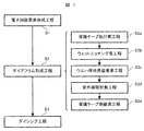
- FIG. 1 is a flow chart showing an example of steps of a method of manufacturing a semiconductor device according to the present invention.
- the method of manufacturing a semiconductor device according to the present invention generally includes an electronic circuit element forming step S1, a diaphragm forming step S2, and a dicing step S3.
- the diaphragm forming step S2 includes a protective tape sticking step S2a, a wafer holder attaching step S2b, a wet etching step S2c, an ultraviolet irradiation step S2d, and a protective tape peeling step S2e.
- This step S1 is a step of forming the electronic circuit element of the MEMS device to be manufactured on one main surface (referred to as a first surface) of the semiconductor wafer.
- a conventional method can be used.
- an electronic circuit element can be formed by ion implantation of dopant atoms using a silicon wafer as a semiconductor wafer.
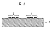
- FIG. 2 is a schematic cross-sectional view showing an example of a semiconductor wafer on which electronic circuit elements are formed. Since the size of a MEMS device is usually about several mm square, for example, if a semiconductor wafer having a diameter of 6 inches is used, several hundreds to about 2000 chips can be obtained from one wafer. That is, as shown in FIG. 2, electronic circuit elements 2 are formed in a large number of regions on the first surface of semiconductor wafer 1.
- the electronic circuit element forming step S1 is not limited to being performed prior to the diaphragm forming step S2, but from the viewpoint of securing a manufacturing yield when the mechanical strength of the diaphragm is low. It is preferable to carry out prior to the diaphragm forming step (in order to prevent breakage of the diaphragm during this step).
- This step S2 is a step of etching and removing the other main surface (referred to as a second surface) of the semiconductor wafer on the back surface side of the region where the electronic circuit element is formed to form a diaphragm.
- the present step S2 includes a plurality of elementary steps S2a to S2e.
- This step S2a protects the first surface of the semiconductor wafer 1 on which the electronic circuit element 2 is formed so that the electronic circuit element 2 is not affected by the wet etching performed later. It is a basic process of sticking a tape.
- the protective tape it is preferable to use a protective tape in which an ultraviolet curable adhesive (for example, an acrylic resin ultraviolet curable adhesive) is laminated on an ultraviolet transparent resin tape (for example, a polyolefin tape). .
- an ultraviolet curable adhesive for example, an acrylic resin ultraviolet curable adhesive
- an ultraviolet transparent resin tape for example, a polyolefin tape.
- a resin tape it is preferable to use a resin tape having heat resistance that the Vicat softening temperature is higher than the etching temperature of the subsequent wet etching.
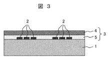
- FIG. 3 is a schematic cross-sectional view showing an example of a semiconductor wafer having a protective tape attached thereto.
- a protective tape 3 (a resin tape 4 and an adhesive layer 5) is attached onto the first surface of the semiconductor wafer 1 on which the electronic circuit element 2 is formed.
- the second surface of the semiconductor wafer 1 may be fixed by vacuum suction or the like, and the second surface of the semiconductor wafer 1 may be attached to the first surface while adjusting the tension so as to prevent the protective tape 3 from being wrinkled.
- This step S2b is a step for mounting the wafer holder on the semiconductor wafer 1 to which the protective tape 3 is attached.
- This step S2b is not an essential step, but is preferably performed from the viewpoint of preventing a decrease in production yield caused by the infiltration of an undesired etching solution from the end of the protective tape 3 during wet etching to be performed later .
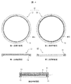
- FIG. 4 is a schematic plan view showing an example of a wafer holder, a schematic sectional view, and a schematic sectional view showing a state in which the wafer holder is mounted on a semiconductor wafer.
- the wafer holder 10 comprises a first jig 11 and a second jig 12, and the second jig 12 has a ring shape in which a region to be etched is largely opened. ing.
- Each of the first jig 11 and the second jig 12 has an O (O) ring 13 made of an elastic material so as to abut on the outer peripheral area of the semiconductor wafer 1, and the outer peripheral area of the semiconductor wafer 1 is a semiconductor wafer It is mounted so as to sandwich it from both surfaces of 1 via the O-ring 13.
- At least the outermost surface of the first jig 11, the second jig 12 and the O-ring 13 is made of a material having chemical resistance so as to withstand immersion in the etching solution.
- a material having chemical resistance so as to withstand immersion in the etching solution.
- PTFE polytetrafluoroethylene
- PPS polyphenylene sulfide
- tool 11 is a disk shape, it is not limited to it, Even if the 1st jig 11 is also a ring shape similarly to the 2nd jig 12 Good.
- the outer shape of the first jig 11 and the second jig 12 is not limited to a circular shape, and may be a quadrangular shape, or a shape capable of mounting a plurality of semiconductor wafers 1. May be
- the wafer holder 10 (the first jig 11 and the second jig 12) preferably has a mechanism for pressing the semiconductor wafer 1 when the wafer holder 10 is mounted on the semiconductor wafer 1.
- a mechanism for pressing it is preferable to use an attractive force by a magnet (for example, a rare earth magnet) built in the wafer holder 10.
- the magnets may be built in both the first jig 11 and the second jig 12 or one of the magnets is built in one and a ferromagnetic material such as iron is built in the other. It may be built in.
- an elastic force by a spring clamp or a clip for holding the wafer holder 10 may be used.
- the pressure of the wafer holder 10 is A mechanism can compensate for the thickness reduction (crush the thickness reduction) to prevent the penetration of the etchant. As a result, it is possible to prevent a decrease in manufacturing yield due to the infiltration of an undesired etching solution.
- This main process S2c is a process which wet-etches the semiconductor wafer 1 from the side of the 2nd surface, and forms a diaphragm in a desired part.
- the wet etching method There is no particular limitation on the wet etching method, and a conventional method can be used.
- the semiconductor wafer 1 is a single crystal silicon wafer, after forming an etching mask in a region which is not etched, it is preferable to perform crystal anisotropic wet etching using a potassium hydroxide aqueous solution or a tetramethyl ammonium hydroxide aqueous solution as an etching solution. It can be used to
- Wet etching is performed by immersing the semiconductor wafer 1 on which the wafer holder 10 is mounted in an etching solution for a length of time corresponding to the etching rate and the intended etching depth.
- the etching temperature (the temperature of the etching solution) is generally controlled to 70 to 80 ° C. in order to improve the etching rate (ie, to shorten the etching time).
- the semiconductor wafer 1 on which the wafer holder 10 is mounted is taken out, and pure water cleaning and drying are performed. Thereafter, the wafer holder 10 is removed.
- the adhesive layer 5 is irradiated with ultraviolet light in order to reduce the adhesive strength of the adhesive layer 5 of the protective tape 3.
- the pressure-sensitive adhesive layer 5 is made of a UV-curable pressure-sensitive adhesive.
- the said ultraviolet curable adhesive shows strong adhesive force before ultraviolet irradiation, when it irradiates an ultraviolet ray, it has the characteristic property that adhesive force falls rapidly.
- a conventional method can be used.
- the present step S2e is a step of peeling the protective tape 3 at a temperature not lower than the etching temperature of the wet etching step S2c and not higher than the Vicat softening temperature of the resin tape 4.
- the present invention is characterized mainly in the step S2e.
- the inventors of the present invention investigated and considered in detail the problem that the ultrathin diaphragm formed by etching at the time of peeling of the protective tape is easily broken in the prior art using the protective tape as the etching protective layer. I understand.
- the protective tape 3 is also naturally heated to the etching temperature. Then, it is considered that the pressure-sensitive adhesive layer 5 of the protective tape 3 is heat-softened, and the surface irregularities resulting from the electronic circuit element 2 are wet and closely fitted. After the wet etching step S2c, the pressure-sensitive adhesive layer 5 is also considered to return from the heat-softened state to the normal state (non-heat-softened state) when returning to the room temperature environment.
- the adhesive force of the adhesive layer 5 is greatly reduced by the ultraviolet irradiation step S2d, it is considered that the adhesive force (so-called anchor effect) resulting from the biting into the surface irregularities of the electronic circuit element 2 remains. Be Then, it is considered that the ultra thin diaphragm is broken due to the anchor effect.
- the present inventors thought that if the pressure-sensitive adhesive layer 5 is returned to a state in which the anchor effect is generated, the pressure-sensitive adhesive layer 5 smoothly separates from the surface unevenness of the electronic circuit element 2. In other words, it was considered that if the pressure-sensitive adhesive layer 5 was thermally softened more than the heat-softened state at the time of wet etching (specifically, if the temperature was raised to the etching temperature or more), it peeled more smoothly.
- the present step S2e at a temperature equal to or higher than the etching temperature of the wet etching step S2c and equal to or lower than the Vicat softening temperature of the resin tape 4.
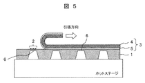
- FIG. 5 is a schematic cross-sectional view showing an outline of the protective tape peeling step.
- the working method of the present step S2e is not particularly limited as long as the above-described temperature conditions are satisfied, and a conventional method can be used.
- the peeling operation can be performed on a hot stage.
- the peeling rate 1 to 30 mm / s can be preferably applied.
- an obtuse angle can be preferably applied as the peeling angle (a complementation of the angle formed by the tension direction of the protective tape and the protective tape in the adhesive state) (the peeling angle in FIG. 5 is 180 °).
- This step S3 is a step of cutting the semiconductor wafer 1 on which the electronic circuit element 2 and the diaphragm 6 (see FIG. 5) are formed into chips.
- the dicing method There is no particular limitation on the dicing method, and a conventional method can be used.
- a 6-inch single crystal silicon wafer is used as the semiconductor wafer 1, and the electronic circuit element forming step S1 to the wet etching step S2c are performed to obtain the electronic circuit element 2 and the diaphragm 6 (thickness: about 2000 chips per wafer). 2 ⁇ m, size: 2 mm square).
- the etching temperature in the wet etching step S2c was 70.degree. When the Vicat softening temperature of the resin tape 4 was examined, it was about 95.degree.
- the protective tape peeling step step S2e was performed under the peeling temperature condition of 50 to 100.degree.
- the peeling angle was 180 ° (see FIG. 5), and the peeling speed was 10 mm / s.
- the damage occurrence rate of the diaphragm 6 was investigated with the diaphragm 6 equivalent to about 10000 chips as a parameter. The breakage incidence rate of less than 0.1% was judged as pass, and the breakage incidence rate of 0.1% or more was judged as failure. The results are shown in Table 1.
- the case where the peeling temperature was 50 to 60 ° C. lower than the etching temperature was a failure. This is considered to be because the heat softening of the pressure-sensitive adhesive layer 5 was insufficient.
- the peeling temperature is 100 ° C., which exceeds the Vicat softening temperature of the resin tape 4, it was a rejection. This is considered to be because the resin tape 4 was distracted and the stress applied to the diaphragm 6 at the time of peeling became uneven.
- 70 to 90 ° C. which is the peeling temperature above the etching temperature and below the Vicat softening temperature of the resin tape 4, it passed.
- the method of manufacturing a semiconductor device according to the present invention contributes to the improvement of the manufacturing yield. Moreover, since the said manufacturing method does not require a special apparatus or a special process if it holds down the point of a protective tape peeling element process, it can be said that it has high workability
- SYMBOLS 1 Semiconductor wafer, 2 ... Electronic-circuit element, 3 ... Protective tape, 4 ... Resin tape, 5 ... Adhesive layer, 6 ... diaphragm, 10 ... wafer holder, 11 ... first jig, 12 ... second jig, 13 ... O-ring.
Landscapes
- Engineering & Computer Science (AREA)
- Manufacturing & Machinery (AREA)
- Physics & Mathematics (AREA)
- Fluid Mechanics (AREA)
- General Physics & Mathematics (AREA)
- Microelectronics & Electronic Packaging (AREA)
- Weting (AREA)
- Pressure Sensors (AREA)
- Measuring Volume Flow (AREA)
- Micromachines (AREA)
Abstract
極薄ダイアフラムを有する半導体デバイスの製造技術において、製造歩留まりの向上に貢献しかつ高い作業容易性を有する製造方法を提供する。 本発明に係る半導体デバイスの製造方法は、ダイアフラムを有する半導体デバイスを製造する方法であって、半導体ウエハの一表面の上に電子回路要素を形成する工程と、前記半導体ウエハの裏面側をエッチング除去して前記ダイアフラムを形成する工程とを有し、前記ダイアフラムを形成する工程は、樹脂テープ上に紫外線硬化型粘着剤層が積層された保護テープを前記半導体ウエハの表面の上に貼り付ける素工程と、前記半導体ウエハを裏面側からウェットエッチングする素工程と、前記粘着剤層に紫外線を照射する素工程と、前記ウェットエッチングのエッチング温度以上かつ前記樹脂テープのビカット軟化温度以下の温度で前記保護テープを剥離する素工程と、を有することを特徴とする。
Description
本発明は、微小電気機械システム(MEMS)の技術に係り、特に、半導体ウエハにダイアフラム構造を形成した半導体デバイスを安定して製造する方法に関するものである。
MEMSとは、一つの基板(例えば、半導体ウエハ)上に、機械要素、センサ要素、電子回路要素などを集積化したデバイスを指す。MEMSデバイスは、応用可能分野が多岐に亘り、近年市場規模が拡大してきていることから、大変注目されている。
MEMSデバイスでは、上述したように、一つの基板上に様々な要素を形成することから、各種の要素を形成する微細加工技術がキーテクノロジーの一つになる。また、それらの微細加工技術においては、微細に加工する技術そのものに加えて、基板をしっかりと保持する技術や、加工しようとする領域以外の領域(非加工領域)を確実に保護する技術も重要である。
例えば、特許文献1(特開平8-255781)には、半導体ウエハの非エッチング面に、シリコーン樹脂をコーティングして保護膜を形成する第1の工程と、前記半導体ウエハをその保護膜側で端面から第1の所定寸法だけかかるリングタイプ治具上にセットする第2の工程と、前記半導体ウエハのエッチング面における端面に第2の所定寸法だけかかるように前記リングタイプ治具との間にシリコーン樹脂をカバーして端面侵食防止膜を形成する第3の工程と、前記端面侵食防止膜が形成された半導体ウエハをエッチング処理する第4の工程と、前記エッチング処理後に前記端面侵食防止膜を剥離して前記リングタイプ治具を取り外と共に、前記保護膜を剥離する第5の工程とを具備する半導体ウエハのエッチング方法、が開示されている。
特許文献1によると、半導体ウエハの端面がエッチング液によって侵かされるのを確実に防止し得るとされている。
特許文献2(特開2004-143223)には、基材フィルム上に、紫外線を照射することによって粘着性が付与され、且つ、加熱により粘着性が低下する粘着剤層を有する半導体ウエハ加工用粘着シートであって、該粘着シートを半導体ウエハに貼着した後、前記半導体ウエハを加工し、しかる後前記粘着シートの粘着剤層を加熱して半導体ウエハから粘着シートを剥離する半導体ウエハの加工方法、が開示されている。
特許文献2によると、半導体ウエハから粘着シートを剥離する際に紫外線の照射を要しないので金属等の非透明な被着体にウエハを貼着することができるとされている。また、加熱により粘着剤層の粘着力が低下するため、容易に半導体ウエハから粘着シートを剥離することができるとされている。
特許文献3(特開2008-60151)には、凹凸形状を有する半導体ウエハ表面に、基材フィルムの片面に粘着剤層を有する放射線硬化型粘着シートを貼り合わせる工程、半導体ウエハ表面に前記放射線硬化型粘着シートを貼り合わせた状態で半導体ウエハ裏面を研削する工程、及び放射線を照射して前記粘着剤層を硬化した後に、前記研削された半導体ウエハ裏面上に表面処理を施す工程を含む半導体ウエハ裏面加工方法、が開示されている。
特許文献3によると、放射線硬化型粘着シートを用いることにより、半導体ウエハの割れや該ウエハ上に糊残り等が生じることなく、高い歩留まりを確保することのできる半導体ウエハ裏面加工が提供できるとされている。
MEMSデバイスの一例として、自動車エンジン用のエアフローセンサがある。該エアフローセンサは、半導体ウエハの一方の主表面上に電子回路要素(例えば、ヒータ抵抗、温度センサ抵抗)が形成されており、該電子回路要素が形成された領域は、半導体ウエハの裏面側がエッチング除去された極薄(例えば、厚さ1~5μm)のダイアフラム構造になっている。言い換えると、該エアフローセンサは、半導体ウエハのうら面側がエッチング除去された極薄ダイアフラムのおもて面側に電子回路要素が形成された構造を有している。エアフローセンサにおける極薄ダイアフラムは、熱容量が小さくなることに起因してセンサの応答速度の向上に寄与することから、性能上意義のある構造と言える。
該エアフローセンサの製造手順は、通常、電子回路要素を半導体ウエハ(例えば、シリコンウエハ)の一方の主表面上に形成する工程の後に、該半導体ウエハの裏面側をウェットエッチング除去してダイアフラム構造を形成する工程を行う。ウェットエッチング工程の際、非加工領域である電子回路要素領域にエッチングの影響が及ばないように、半導体ウエハの表面側をエッチング保護層(例えば、保護ワックス、保護テープ)で被覆する。ウェットエッチング工程の後、エッチング保護層を剥離する工程を行う。その後、該半導体ウエハをチップ状に切断するダイシング工程を行う。
ここで、半導体ウエハに形成された該ダイアフラムは、厚さが非常に薄くその機械的強度が非常に小さいことから、エッチング保護層の剥離工程中に破損し易いという問題があった。そのため、エアフローセンサの製造歩留まり向上の観点から極薄ダイアフラムを破損させずに、かつ簡便にエッチング保護層を除去するプロセスの開発が望まれていた。
特許文献1~3で開示された技術は、それぞれの文献に記載された範囲の作用効果を有すると考えられる。しかしながら、本発明者等が検討したところ、特許文献1~3の単独技術およびそれらの単純組合せの技術は、極薄ダイアフラムの破損防止および/または作業容易性(作業コスト)の観点で、残念ながら要求レベルを満足できるものではなかった。
一方、エッチング保護層として保護ワックスを用いる場合、保護ワックスの塗布および塗布した保護ワックスの除去の際に、電子回路要素を傷付け易いという難点があった。また、保護ワックスの除去の際に、電子回路要素に起因する表面凹凸に一部の保護ワックスが残存し易いという問題があった。これらは、いずれも製造歩留まりの低下要因となる。
したがって、本発明の目的は、極薄ダイアフラムを有する半導体デバイスの製造技術において、製造歩留まりの向上に貢献しかつ高い作業容易性を有する製造方法を提供することにある。
本発明の一態様は、ダイアフラムを有する半導体デバイスを製造する方法であって、半導体ウエハの第一表面の上に電子回路要素を形成する電子回路要素形成工程と、前記電子回路要素が形成された領域の裏面側で前記半導体ウエハの第二表面をエッチング除去して前記ダイアフラムを形成するダイアフラム形成工程とを有し、前記ダイアフラム形成工程は、紫外線透過性の樹脂テープの上に紫外線硬化型の粘着剤層が積層された保護テープを前記半導体ウエハの第一表面の上に貼り付ける保護テープ貼付素工程と、前記半導体ウエハを前記第二表面の側からウェットエッチングするウェットエッチング素工程と、前記粘着剤層の粘着力を低下させるために該粘着剤層に紫外線を照射する紫外線照射素工程と、前記ウェットエッチング素工程のエッチング温度以上かつ前記樹脂テープのビカット軟化温度以下の温度で前記保護テープを剥離する保護テープ剥離素工程と、を有することを特徴とする半導体デバイスの製造方法、を提供する。
本発明によれば、極薄ダイアフラムを有する半導体デバイスの製造技術において、製造歩留まりの向上に貢献しかつ高い作業容易性を有する製造方法を提供することができる。
本発明は、前述した半導体デバイスの製造方法において、以下のような改良や変更を加えることができる。
(i)前記ダイアフラム形成工程は、前記保護テープ貼付素工程と前記ウェットエッチング素工程との間に、前記保護テープが貼り付けられた前記半導体ウエハに対してウエハ保持具を装着するウエハ保持具装着素工程を更に有し、前記ウエハ保持具は、該半導体ウエハの外周領域を該半導体ウエハの両表面からO(オウ)リングを介して挟み込んで押圧する機構を有する。
(ii)前記ウエハ保持具における前記押圧する機構は、該ウエハ保持具に内蔵された磁石による引力である。
(iii)前記ウエハ保持具における前記押圧する機構は、該ウエハ保持具に装着されたばねクランプによる弾性力である。
(iv)前記ダイアフラムは、厚さが1μm以上5μm以下であり、大きさが1 mm角以上4 mm角以下である。
(v)前記樹脂テープは、前記ビカット軟化温度が前記エッチング温度よりも高いという耐熱性を有する。
(vi)前記半導体ウエハは、単結晶シリコンウエハであり、前記ウェットエッチング素工程のエッチング液は、水酸化カリウム水溶液または水酸化テトラメチルアンモニウム水溶液である。
(vii)前記半導体デバイスは、エアフローセンサである。
以下、ダイアフラムを有する半導体デバイスの例としてエアフローセンサを対象とし、本発明に係る実施形態について図面を参照しながら説明する。ただし、本発明はここで取り上げた実施形態に限定されることはなく、発明の技術的思想を逸脱しない範囲で、公知技術と適宜組み合わせたり公知技術に基づいて改良したりすることが可能である。
[半導体デバイスの製造方法]
図1は、本発明に係る半導体デバイスの製造方法の工程例を示すフロー図である。図1に示したように、本発明に係る半導体デバイスの製造方法は、概略的に、電子回路要素形成工程S1と、ダイアフラム形成工程S2と、ダイシング工程S3とを有する。また、ダイアフラム形成工程S2は、保護テープ貼付素工程S2aと、ウエハ保持具装着素工程S2bと、ウェットエッチング素工程S2cと、紫外線照射素工程S2dと、保護テープ剥離素工程S2eとを含む。以下、各工程・素工程についてより具体的に説明する。
図1は、本発明に係る半導体デバイスの製造方法の工程例を示すフロー図である。図1に示したように、本発明に係る半導体デバイスの製造方法は、概略的に、電子回路要素形成工程S1と、ダイアフラム形成工程S2と、ダイシング工程S3とを有する。また、ダイアフラム形成工程S2は、保護テープ貼付素工程S2aと、ウエハ保持具装着素工程S2bと、ウェットエッチング素工程S2cと、紫外線照射素工程S2dと、保護テープ剥離素工程S2eとを含む。以下、各工程・素工程についてより具体的に説明する。
(電子回路要素形成工程)
本工程S1は、半導体ウエハの一方の主表面(第一表面と称す)の上に、製造対象とするMEMSデバイスの電子回路要素を形成する工程である。電子回路要素の形成方法に特段の限定はなく、従前の方法を利用できる。例えば、半導体ウエハとしてシリコンウエハを用い、ドーパント原子のイオン注入により電子回路要素を形成することができる。
本工程S1は、半導体ウエハの一方の主表面(第一表面と称す)の上に、製造対象とするMEMSデバイスの電子回路要素を形成する工程である。電子回路要素の形成方法に特段の限定はなく、従前の方法を利用できる。例えば、半導体ウエハとしてシリコンウエハを用い、ドーパント原子のイオン注入により電子回路要素を形成することができる。
図2は、電子回路要素を形成した半導体ウエハの一例を示す概略断面図である。MEMSデバイスは、通常、その大きさが数mm角程度であることから、例えば、6インチ径の半導体ウエハを用いると、1枚のウエハから数100~2000個程度のチップが得られる。すなわち、図2に示したように、半導体ウエハ1の第一表面の上に電子回路要素2が多数領域で形成される。
なお、本発明において、電子回路要素形成工程S1は、ダイアフラム形成工程S2よりも前に行うことに限定されるものではないが、ダイアフラムの機械的強度が低い場合は、製造歩留まりを確保する観点から(本工程中でのダイアフラムの破損を防止するため)、ダイアフラム形成工程よりも前に行うことが好ましい。
(ダイアフラム形成工程)
本工程S2は、電子回路要素が形成された領域の裏面側で半導体ウエハの他方の主表面(第二表面と称す)をエッチング除去してダイアフラムを形成する工程である。前述したように、本工程S2は、複数の素工程S2a~S2eを含む。
本工程S2は、電子回路要素が形成された領域の裏面側で半導体ウエハの他方の主表面(第二表面と称す)をエッチング除去してダイアフラムを形成する工程である。前述したように、本工程S2は、複数の素工程S2a~S2eを含む。
(1)保護テープ貼付素工程
本素工程S2aは、電子回路要素2が後に行うウェットエッチングの影響を受けないように、電子回路要素2が形成された半導体ウエハ1の第一表面の上に保護テープを貼り付ける素工程である。保護テープとしては、紫外線透過性の樹脂テープ(例えば、ポリオレフィンテープ)の上に紫外線硬化型の粘着剤(例えば、アクリル樹脂系の紫外線硬化型粘着剤)が積層された保護テープを用いることが好ましい。また、樹脂テープとしては、そのビカット軟化温度が後のウェットエッチングのエッチング温度よりも高いという耐熱性を有する樹脂テープを用いることが好ましい。
本素工程S2aは、電子回路要素2が後に行うウェットエッチングの影響を受けないように、電子回路要素2が形成された半導体ウエハ1の第一表面の上に保護テープを貼り付ける素工程である。保護テープとしては、紫外線透過性の樹脂テープ(例えば、ポリオレフィンテープ)の上に紫外線硬化型の粘着剤(例えば、アクリル樹脂系の紫外線硬化型粘着剤)が積層された保護テープを用いることが好ましい。また、樹脂テープとしては、そのビカット軟化温度が後のウェットエッチングのエッチング温度よりも高いという耐熱性を有する樹脂テープを用いることが好ましい。
図3は、保護テープを貼り付けた半導体ウエハの一例を示す概略断面図である。図3に示すように、半導体ウエハ1の電子回路要素2が形成された第一表面の上に保護テープ3(樹脂テープ4、粘着剤層5)が貼り付けられている。
保護テープ3の貼付方法に特段の限定はなく、従前の方法を利用できる。例えば、半導体ウエハ1の第二表面を真空吸着等で固定し、保護テープ3にしわ等が入らないように張力を調整しながら第一表面の上に貼り付ければよい。また、半導体ウエハ1の外形からはみ出した保護テープ3の余剰部分は、半導体ウエハ1の外形に沿って切除することが望ましい。
(2)ウエハ保持具装着素工程
本素工程S2bは、保護テープ3が貼り付けられた半導体ウエハ1に対してウエハ保持具を装着する素工程である。本素工程S2bは、必須の素工程ではないが、後に行うウェットエッチング中に保護テープ3の端からの望まないエッチング液の浸入に起因した製造歩留まりの低下を防止する観点から、行うことが好ましい。
本素工程S2bは、保護テープ3が貼り付けられた半導体ウエハ1に対してウエハ保持具を装着する素工程である。本素工程S2bは、必須の素工程ではないが、後に行うウェットエッチング中に保護テープ3の端からの望まないエッチング液の浸入に起因した製造歩留まりの低下を防止する観点から、行うことが好ましい。
図4は、ウエハ保持具の一例を示す平面模式図、断面模式図および半導体ウエハにウエハ保持具を装着した状態を示す断面模式図である。図4に示したように、ウエハ保持具10は、第一治具11と第二治具12とからなり、第二治具12は、エッチングしようとする領域が大きく開口したリング形状を有している。第一治具11および第二治具12のそれぞれは、半導体ウエハ1の外周領域と当接するように弾性材のO(オウ)リング13を具備しており、半導体ウエハ1の外周領域を半導体ウエハ1の両表面からOリング13を介して挟み込むように装着される。
第一治具11、第二治具12およびOリング13は、エッチング液への浸漬に耐えられるように、少なくとも最表面が耐薬品性を有する素材で構成されていることが好ましい。例えば、ポリテトラフルオロエチレン(PTFE)やポリフェニレンサルファイド(PPS)を好適に用いることができる。
なお、図4においては、第一治具11が円盤形状になっているが、それに限定されるものではなく、第二治具12と同様に第一治具11もリング形状になっていてもよい。また、第一治具11および第二治具12の外形は、円形状に限定されるものではなく、四角形状であってもよいし、複数枚の半導体ウエハ1を装着できるような形状であってもよい。
ウエハ保持具10(第一治具11、第二治具12)は、半導体ウエハ1への装着時に、半導体ウエハ1を押圧する機構を有していることが好ましい。押圧する機構としては、ウエハ保持具10に内蔵された磁石(例えば、希土類磁石)による引力を利用することが好ましい。ウエハ保持具10に磁石を内蔵する場合、第一治具11および第二治具12の両方に磁石を内蔵してもよいし、一方に磁石を内蔵して他方に鉄等の強磁性体を内蔵してもよい。
また、他の押圧する機構として、ウエハ保持具10を挟み込むばねクランプまたはクリップによる弾性力を利用してもよい。
ウエハ保持具10が押圧機構を有することにより、仮にウェットエッチング中に保護テープ3の端部で粘着剤層5がエッチング液に溶出して厚さが薄くなったとしても、ウエハ保持具10の押圧機構がその厚さ減少分を補填して(厚さ減少分を押し潰して)、エッチング液の浸入を防止することができる。その結果、望まないエッチング液の浸入に起因した製造歩留まりの低下を防止することができる。
(3)ウェットエッチング素工程
本素工程S2cは、半導体ウエハ1を第二表面の側からウェットエッチングして所望箇所にダイアフラムを形成する素工程である。ウェットエッチング方法に特段の限定はなく、従前の方法を利用できる。例えば、半導体ウエハ1が単結晶シリコンウエハである場合、エッチングしない領域にエッチングマスクを形成した後、エッチング液として水酸化カリウム水溶液または水酸化テトラメチルアンモニウム水溶液を用いた結晶異方性ウェットエッチングを好適に利用することができる。
本素工程S2cは、半導体ウエハ1を第二表面の側からウェットエッチングして所望箇所にダイアフラムを形成する素工程である。ウェットエッチング方法に特段の限定はなく、従前の方法を利用できる。例えば、半導体ウエハ1が単結晶シリコンウエハである場合、エッチングしない領域にエッチングマスクを形成した後、エッチング液として水酸化カリウム水溶液または水酸化テトラメチルアンモニウム水溶液を用いた結晶異方性ウェットエッチングを好適に利用することができる。
エッチング速度および予定するエッチング深さに応じた時間長さで、ウエハ保持具10を装着した半導体ウエハ1をエッチング液に浸漬してウェットエッチングが行われる。なお、エッチング速度向上(すなわち、エッチング時間短縮)のため、エッチング温度(エッチング液の温度)は一般的に70~80℃に制御される。
所定時間のウェットエッチングを行った後、ウエハ保持具10を装着した半導体ウエハ1を取り出し、純水洗浄および乾燥を行う。その後、ウエハ保持具10を取り外す。
(4)紫外線照射素工程
本素工程S2dは、保護テープ3の粘着剤層5の粘着力を低下させるために粘着剤層5に紫外線を照射する素工程である。前述したように、粘着剤層5は紫外線硬化型粘着剤からなる。当該紫外線硬化型粘着剤は、紫外線照射前は強力な粘着力を示すが、紫外線を照射すると粘着力が急激に低下するという特徴的な性質を有する。紫外線照射の方法に特段の限定はなく、従前の方法を利用できる。本素工程S2dで粘着剤層5の粘着力を低下させることにより、保護テープ3を剥離する前準備とする。
本素工程S2dは、保護テープ3の粘着剤層5の粘着力を低下させるために粘着剤層5に紫外線を照射する素工程である。前述したように、粘着剤層5は紫外線硬化型粘着剤からなる。当該紫外線硬化型粘着剤は、紫外線照射前は強力な粘着力を示すが、紫外線を照射すると粘着力が急激に低下するという特徴的な性質を有する。紫外線照射の方法に特段の限定はなく、従前の方法を利用できる。本素工程S2dで粘着剤層5の粘着力を低下させることにより、保護テープ3を剥離する前準備とする。
(5)保護テープ剥離素工程
本素工程S2eは、ウェットエッチング素工程S2cのエッチング温度以上かつ樹脂テープ4のビカット軟化温度以下の温度で保護テープ3を剥離する素工程である。本発明は、この素工程S2eに大きな特徴がある。
本素工程S2eは、ウェットエッチング素工程S2cのエッチング温度以上かつ樹脂テープ4のビカット軟化温度以下の温度で保護テープ3を剥離する素工程である。本発明は、この素工程S2eに大きな特徴がある。
本発明者等は、エッチング保護層として保護テープを用いた従来技術において、保護テープの剥離時にエッチング形成した極薄ダイアフラムが破損し易い問題について、詳細に調査・考察したところ、次のようなことが判った。
ウェットエッチング素工程S2cのウェットエッチング中、半導体ウエハ1がエッチング温度に昇温されることに加えて、当然のことながら保護テープ3も当該エッチング温度に昇温される。すると、保護テープ3の粘着剤層5が熱軟化して、電子回路要素2に起因する表面凹凸にぴったりと濡れ馴染むと考えられる。ウェットエッチング素工程S2cの後、室温環境に戻ると粘着剤層5も熱軟化状態から通常状態(熱軟化していない状態)に戻ると考えられる。
その後、紫外線照射素工程S2dにより、粘着剤層5の粘着力は大きく低下するが、電子回路要素2の表面凹凸に食い込んだことに起因する固着力(いわゆるアンカー効果)は、残存するものと考えられる。そして、該アンカー効果に起因して極薄ダイアフラムが破損したものと考えられる。
そこで、本発明者等は、アンカー効果が生じる基となった状態に粘着剤層5を戻せば、粘着剤層5が電子回路要素2の表面凹凸からスムーズに剥がれると考えた。言い換えると、粘着剤層5をウェットエッチング時の熱軟化状態以上に熱軟化させれば(具体的には、エッチング温度以上に昇温すれば)、よりスムーズに剥がれると考えた。
一方、本発明者等による種々の実験の結果、保護テープ剥離素工程の温度を上げていくと、樹脂テープ4が伸延し始めて剥離の応力伝搬が不均一になり(ところどころに剥離の応力集中点が生じるようになり)、かえって極薄ダイアフラムが破損し易くなることが判った。そして、樹脂テープ4が伸延し始める温度としては、樹脂テープ4のビカット軟化温度(JIS K7206により測定可能)と強く関連していることを見出した。
これらのことから、本素工程S2eは、ウェットエッチング素工程S2cのエッチング温度以上かつ樹脂テープ4のビカット軟化温度以下の温度で行うことが好ましい。
図5は、保護テープ剥離素工程の概略を示す断面模式図である。図5に示したように、本素工程S2eの作業方法は、上述の温度条件を満たせば特段の限定はなく、従前の方法を利用できる。例えば、温度制御方法として、ホットステージ上で剥離作業を行うことができる。剥離速度としては、1~30 mm/sを好ましく適用できる。また、剥離角度(保護テープの引張方向と接着状態の保護テープとのなす角の補角)としては、鈍角を好ましく適用できる(図5における剥離角度は180°である)。
(ダイシング工程)
本工程S3は、電子回路要素2とダイアフラム6(図5参照)とが形成された半導体ウエハ1をチップ状に切断する工程である。ダイシング方法に特段の限定はなく、従前の方法を利用できる。
本工程S3は、電子回路要素2とダイアフラム6(図5参照)とが形成された半導体ウエハ1をチップ状に切断する工程である。ダイシング方法に特段の限定はなく、従前の方法を利用できる。
以下、実験例により本発明をさらに具体的に説明する。なお、本発明はこれらの実験例に限定されるものではない。
半導体ウエハ1として6インチの単結晶シリコンウエハを用い、電子回路要素形成工程S1~ウェットエッチング素工程S2cを行って、ウエハ1枚あたり約2000チップ相当の電子回路要素2とダイアフラム6(厚さ:2μm、サイズ:2 mm角)とを形成した。ウェットエッチング素工程S2cにおけるエッチング温度は70℃とした。樹脂テープ4のビカット軟化温度を調べたところ、約95℃であった。
次に、紫外線照射素工程S2dを行った後、50~100℃の剥離温度条件で保護テープ剥離素工程S2eを行った。剥離角度は180°(図5参照)とし、剥離速度は10 mm/sとした。各剥離温度において、約10000チップ相当のダイアフラム6を母数としてダイアフラム6の破損発生率を調査した。破損発生率0.1%未満を合格と判定し、破損発生率0.1%以上を不合格と判定した。結果を表1に示す。

表1に示したように、剥離温度がエッチング温度よりも低い50~60℃の場合は、不合格であった。これは、粘着剤層5の熱軟化が不十分でであったためと考えられる。一方、剥離温度が樹脂テープ4のビカット軟化温度を超える100℃の場合も、不合格であった。これは、樹脂テープ4の伸延が生じ、剥離時にダイアフラム6に掛かる応力が不均一になったためと考えられる。これらに対し、剥離温度がエッチング温度以上で樹脂テープ4のビカット軟化温度以下である70~90℃の場合は、合格であった。
以上の実験から、本発明に係る半導体デバイスの製造方法は、製造歩留まりの向上に寄与することが確認された。また、当該製造方法は、保護テープ剥離素工程のポイントを押さえれば、特殊な装置や特殊な工程を必要としないことから、高い作業容易性を有すると言える。
1…半導体ウエハ、2…電子回路要素、3…保護テープ、4…樹脂テープ、5…粘着剤層、
6…ダイアフラム、10…ウエハ保持具、11…第一治具、12…第二治具、13…Oリング。
6…ダイアフラム、10…ウエハ保持具、11…第一治具、12…第二治具、13…Oリング。
Claims (8)
- ダイアフラムを有する半導体デバイスを製造する方法であって、半導体ウエハの第一表面の上に電子回路要素を形成する電子回路要素形成工程と、前記電子回路要素が形成された領域の裏面側で前記半導体ウエハの第二表面をエッチング除去して前記ダイアフラムを形成するダイアフラム形成工程とを有し、前記ダイアフラム形成工程は、紫外線透過性の樹脂テープの上に紫外線硬化型の粘着剤層が積層された保護テープを前記半導体ウエハの第一表面の上に貼り付ける保護テープ貼付素工程と、前記半導体ウエハを前記第二表面の側からウェットエッチングするウェットエッチング素工程と、前記粘着剤層の粘着力を低下させるために該粘着剤層に紫外線を照射する紫外線照射素工程と、前記ウェットエッチング素工程のエッチング温度以上かつ前記樹脂テープのビカット軟化温度以下の温度で前記保護テープを剥離する保護テープ剥離素工程と、を有することを特徴とする半導体デバイスの製造方法。
- 請求項1に記載の半導体デバイスの製造方法において、前記ダイアフラム形成工程は、前記保護テープ貼付素工程と前記ウェットエッチング素工程との間に、前記保護テープが貼り付けられた前記半導体ウエハに対してウエハ保持具を装着するウエハ保持具装着素工程を更に有し、前記ウエハ保持具は、該半導体ウエハの外周領域を該半導体ウエハの両表面からOリングを介して挟み込んで押圧する機構を有することを特徴とする半導体デバイスの製造方法。
- 請求項2に記載の半導体デバイスの製造方法において、前記ウエハ保持具における前記押圧する機構は、該ウエハ保持具に内蔵された磁石による引力であることを特徴とする半導体デバイスの製造方法。
- 請求項2に記載の半導体デバイスの製造方法において、前記ウエハ保持具における前記押圧する機構は、該ウエハ保持具に装着されたばねクランプによる弾性力であることを特徴とする半導体デバイスの製造方法。
- 請求項1乃至請求項4のいずれか一項に記載の半導体デバイスの製造方法において、前記ダイアフラムは、厚さが1μm以上5μm以下であり、大きさが1 mm角以上4 mm角以下であることを特徴とする半導体デバイスの製造方法。
- 請求項1乃至請求項5のいずれか一項に記載の半導体デバイスの製造方法において、前記樹脂テープは、前記ビカット軟化温度が前記エッチング温度よりも高いという耐熱性を有することを特徴とする半導体デバイスの製造方法。
- 請求項1乃至請求項5のいずれか一項に記載の半導体デバイスの製造方法において、前記半導体ウエハは、単結晶シリコンウエハであり、前記ウェットエッチング素工程のエッチング液は、水酸化カリウム水溶液または水酸化テトラメチルアンモニウム水溶液であることを特徴とする半導体デバイスの製造方法。
- 請求項1乃至請求項5のいずれか一項に記載の半導体デバイスの製造方法において、前記半導体デバイスは、エアフローセンサであることを特徴とする半導体デバイスの製造方法。
Priority Applications (2)
| Application Number | Priority Date | Filing Date | Title |
|---|---|---|---|
| DE112018005482.9T DE112018005482T5 (de) | 2017-09-28 | 2018-08-01 | Verfahren zum herstellen einer halbleitervorrichtung |
| JP2019544360A JPWO2019064906A1 (ja) | 2017-09-28 | 2018-08-01 | 半導体デバイスの製造方法 |
Applications Claiming Priority (2)
| Application Number | Priority Date | Filing Date | Title |
|---|---|---|---|
| JP2017187802 | 2017-09-28 | ||
| JP2017-187802 | 2017-09-28 |
Publications (1)
| Publication Number | Publication Date |
|---|---|
| WO2019064906A1 true WO2019064906A1 (ja) | 2019-04-04 |
Family
ID=65903809
Family Applications (1)
| Application Number | Title | Priority Date | Filing Date |
|---|---|---|---|
| PCT/JP2018/028793 Ceased WO2019064906A1 (ja) | 2017-09-28 | 2018-08-01 | 半導体デバイスの製造方法 |
Country Status (3)
| Country | Link |
|---|---|
| JP (1) | JPWO2019064906A1 (ja) |
| DE (1) | DE112018005482T5 (ja) |
| WO (1) | WO2019064906A1 (ja) |
Citations (6)
| Publication number | Priority date | Publication date | Assignee | Title |
|---|---|---|---|---|
| JP2006013115A (ja) * | 2004-06-25 | 2006-01-12 | Seiko Epson Corp | エッチング方法及び微細構造体の製造方法 |
| JP2006303410A (ja) * | 2005-03-25 | 2006-11-02 | Fuji Electric Holdings Co Ltd | 半導体装置およびその製造方法 |
| JP2008135662A (ja) * | 2006-11-29 | 2008-06-12 | Nitto Denko Corp | 粘着シートの貼付・剥離方法及び粘着シートの貼付装置並びに粘着シートの剥離装置 |
| JP2008218919A (ja) * | 2007-03-07 | 2008-09-18 | Nec Electronics Corp | 半導体ウエハの表面保護方法および表面保護構造 |
| JP2010067782A (ja) * | 2008-09-10 | 2010-03-25 | Tokyo Seimitsu Co Ltd | 表面保護フィルム剥離装置 |
| JP2011124480A (ja) * | 2009-12-14 | 2011-06-23 | Nitto Denko Corp | 粘着テープ剥離方法およびその装置 |
-
2018
- 2018-08-01 JP JP2019544360A patent/JPWO2019064906A1/ja not_active Ceased
- 2018-08-01 DE DE112018005482.9T patent/DE112018005482T5/de not_active Withdrawn
- 2018-08-01 WO PCT/JP2018/028793 patent/WO2019064906A1/ja not_active Ceased
Patent Citations (6)
| Publication number | Priority date | Publication date | Assignee | Title |
|---|---|---|---|---|
| JP2006013115A (ja) * | 2004-06-25 | 2006-01-12 | Seiko Epson Corp | エッチング方法及び微細構造体の製造方法 |
| JP2006303410A (ja) * | 2005-03-25 | 2006-11-02 | Fuji Electric Holdings Co Ltd | 半導体装置およびその製造方法 |
| JP2008135662A (ja) * | 2006-11-29 | 2008-06-12 | Nitto Denko Corp | 粘着シートの貼付・剥離方法及び粘着シートの貼付装置並びに粘着シートの剥離装置 |
| JP2008218919A (ja) * | 2007-03-07 | 2008-09-18 | Nec Electronics Corp | 半導体ウエハの表面保護方法および表面保護構造 |
| JP2010067782A (ja) * | 2008-09-10 | 2010-03-25 | Tokyo Seimitsu Co Ltd | 表面保護フィルム剥離装置 |
| JP2011124480A (ja) * | 2009-12-14 | 2011-06-23 | Nitto Denko Corp | 粘着テープ剥離方法およびその装置 |
Also Published As
| Publication number | Publication date |
|---|---|
| DE112018005482T5 (de) | 2020-10-15 |
| JPWO2019064906A1 (ja) | 2020-04-02 |
Similar Documents
| Publication | Publication Date | Title |
|---|---|---|
| JP5379377B2 (ja) | 表面保護用シートおよび半導体ウエハの研削方法 | |
| KR20060120113A (ko) | 표면보호용 시트 및 반도체 웨이퍼의 연삭방법 | |
| JP2009188010A (ja) | 脆質部材用支持体および脆質部材の処理方法 | |
| US10083850B2 (en) | Method of forming a flexible semiconductor layer and devices on a flexible carrier | |
| US9553008B1 (en) | Methods to reduce debonding forces on flexible semiconductor films disposed on vapor-releasing adhesives | |
| JP2008078430A (ja) | 電子部品の製造方法 | |
| JP2003209073A (ja) | 半導体ウエハの加工方法 | |
| JP5074719B2 (ja) | ウエハを薄くする方法及びサポートプレート | |
| JP5704602B2 (ja) | 薄型半導体装置の製造方法および脆質部材用支持体 | |
| CN103999195B (zh) | 将粘合膜在切割带上制备成预切割的半导体晶圆形状的方法 | |
| TWI354325B (ja) | ||
| CN104364880B (zh) | Soi晶片的制造方法 | |
| JPWO2019064906A1 (ja) | 半導体デバイスの製造方法 | |
| JP2011219503A (ja) | 粘着テープ | |
| JP2010067782A (ja) | 表面保護フィルム剥離装置 | |
| JP2005243910A (ja) | 半導体チップの製造方法 | |
| JP7657032B2 (ja) | 保持具、保持方法、及び加工方法 | |
| JP2004063678A (ja) | 脆質部材からの表面保護テープの剥離方法 | |
| US20170098591A1 (en) | Method of manufacturing element chip and element chip | |
| JP2002134451A (ja) | 半導体装置の製造方法 | |
| JP5193753B2 (ja) | ダイシングシートおよび半導体チップの製造方法 | |
| JP2006261482A (ja) | 半導体ウェハ表面保護フィルム及び該保護フィルムを用いる半導体ウェハの保護方法 | |
| US20250253182A1 (en) | Method for manufacturing semiconductor device | |
| US20230377935A1 (en) | Temporary bonding method | |
| JP2010062415A (ja) | 保護テープの剥離方法、及び、半導体装置の製造方法 |
Legal Events
| Date | Code | Title | Description |
|---|---|---|---|
| 121 | Ep: the epo has been informed by wipo that ep was designated in this application |
Ref document number: 18863413 Country of ref document: EP Kind code of ref document: A1 |
|
| ENP | Entry into the national phase |
Ref document number: 2019544360 Country of ref document: JP Kind code of ref document: A |
|
| 122 | Ep: pct application non-entry in european phase |
Ref document number: 18863413 Country of ref document: EP Kind code of ref document: A1 |