WO2019064844A1 - 採光システム - Google Patents
採光システム Download PDFInfo
- Publication number
- WO2019064844A1 WO2019064844A1 PCT/JP2018/027225 JP2018027225W WO2019064844A1 WO 2019064844 A1 WO2019064844 A1 WO 2019064844A1 JP 2018027225 W JP2018027225 W JP 2018027225W WO 2019064844 A1 WO2019064844 A1 WO 2019064844A1
- Authority
- WO
- WIPO (PCT)
- Prior art keywords
- light distribution
- light
- electrode layers
- emission angle
- layer
- Prior art date
- Legal status (The legal status is an assumption and is not a legal conclusion. Google has not performed a legal analysis and makes no representation as to the accuracy of the status listed.)
- Ceased
Links
Images



Classifications
-
- G—PHYSICS
- G02—OPTICS
- G02F—OPTICAL DEVICES OR ARRANGEMENTS FOR THE CONTROL OF LIGHT BY MODIFICATION OF THE OPTICAL PROPERTIES OF THE MEDIA OF THE ELEMENTS INVOLVED THEREIN; NON-LINEAR OPTICS; FREQUENCY-CHANGING OF LIGHT; OPTICAL LOGIC ELEMENTS; OPTICAL ANALOGUE/DIGITAL CONVERTERS
- G02F1/00—Devices or arrangements for the control of the intensity, colour, phase, polarisation or direction of light arriving from an independent light source, e.g. switching, gating or modulating; Non-linear optics
- G02F1/01—Devices or arrangements for the control of the intensity, colour, phase, polarisation or direction of light arriving from an independent light source, e.g. switching, gating or modulating; Non-linear optics for the control of the intensity, phase, polarisation or colour
- G02F1/13—Devices or arrangements for the control of the intensity, colour, phase, polarisation or direction of light arriving from an independent light source, e.g. switching, gating or modulating; Non-linear optics for the control of the intensity, phase, polarisation or colour based on liquid crystals, e.g. single liquid crystal display cells
-
- G—PHYSICS
- G02—OPTICS
- G02F—OPTICAL DEVICES OR ARRANGEMENTS FOR THE CONTROL OF LIGHT BY MODIFICATION OF THE OPTICAL PROPERTIES OF THE MEDIA OF THE ELEMENTS INVOLVED THEREIN; NON-LINEAR OPTICS; FREQUENCY-CHANGING OF LIGHT; OPTICAL LOGIC ELEMENTS; OPTICAL ANALOGUE/DIGITAL CONVERTERS
- G02F1/00—Devices or arrangements for the control of the intensity, colour, phase, polarisation or direction of light arriving from an independent light source, e.g. switching, gating or modulating; Non-linear optics
- G02F1/01—Devices or arrangements for the control of the intensity, colour, phase, polarisation or direction of light arriving from an independent light source, e.g. switching, gating or modulating; Non-linear optics for the control of the intensity, phase, polarisation or colour
- G02F1/165—Devices or arrangements for the control of the intensity, colour, phase, polarisation or direction of light arriving from an independent light source, e.g. switching, gating or modulating; Non-linear optics for the control of the intensity, phase, polarisation or colour based on translational movement of particles in a fluid under the influence of an applied field
- G02F1/166—Devices or arrangements for the control of the intensity, colour, phase, polarisation or direction of light arriving from an independent light source, e.g. switching, gating or modulating; Non-linear optics for the control of the intensity, phase, polarisation or colour based on translational movement of particles in a fluid under the influence of an applied field characterised by the electro-optical or magneto-optical effect
- G02F1/167—Devices or arrangements for the control of the intensity, colour, phase, polarisation or direction of light arriving from an independent light source, e.g. switching, gating or modulating; Non-linear optics for the control of the intensity, phase, polarisation or colour based on translational movement of particles in a fluid under the influence of an applied field characterised by the electro-optical or magneto-optical effect by electrophoresis
-
- G—PHYSICS
- G02—OPTICS
- G02F—OPTICAL DEVICES OR ARRANGEMENTS FOR THE CONTROL OF LIGHT BY MODIFICATION OF THE OPTICAL PROPERTIES OF THE MEDIA OF THE ELEMENTS INVOLVED THEREIN; NON-LINEAR OPTICS; FREQUENCY-CHANGING OF LIGHT; OPTICAL LOGIC ELEMENTS; OPTICAL ANALOGUE/DIGITAL CONVERTERS
- G02F1/00—Devices or arrangements for the control of the intensity, colour, phase, polarisation or direction of light arriving from an independent light source, e.g. switching, gating or modulating; Non-linear optics
- G02F1/29—Devices or arrangements for the control of the intensity, colour, phase, polarisation or direction of light arriving from an independent light source, e.g. switching, gating or modulating; Non-linear optics for the control of the position or the direction of light beams, i.e. deflection
Definitions
- the present invention relates to a daylighting system capable of controlling the outgoing angle of light incident on a functional film.
- Patent Document 1 discloses a light control device capable of changing the transmission region and the non-transmission region by controlling the voltage applied between the electrodes. Such a light control device is used, for example, for anti-west day measures or privacy protection.
- the light control device described above does not have a high degree of freedom in the distribution of light entering the room.
- the present invention provides a daylighting system in which the degree of freedom of light distribution entering a room is enhanced.
- a lighting system includes a first region having a laminated structure in which a first light distribution control layer is located between two first electrode layers, and a second region between two second electrode layers. Control a voltage applied to each of a functional film including a second region having a laminated structure in which a light distribution control layer is located, the two first electrode layers, and the two second electrode layers And a driving device for independently controlling a first emission angle of light incident on the first light distribution control layer and a second emission angle of light incident on the second light distribution control layer.
- a daylighting system is realized in which the degree of freedom of the light distribution of light entering the room is enhanced.
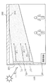
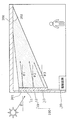
- FIG. 1A is a view showing a light distribution pattern A by the lighting system according to the embodiment.
- FIG. 1B is a view showing a light distribution pattern B by the lighting system according to the embodiment.
- FIG. 1C is a view showing a light distribution pattern C by the lighting system according to the embodiment.
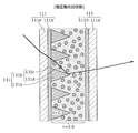
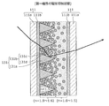
- FIG. 2 is a schematic cross section which shows the detailed structure of the functional film with which the lighting system which concerns on embodiment is equipped.
- FIG. 3A is a diagram for explaining the traveling direction of light in the no voltage application state.
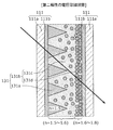
- FIG. 3B is a diagram for explaining the traveling direction of light in the voltage application state.
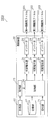
- FIG. 4 is a block diagram showing a functional configuration of the daylighting system according to the embodiment.
- FIG. 5 is a flowchart of the operation of the daylighting system according to the embodiment.
- FIG. 6 is a diagram showing an example of light distribution pattern information.
- FIG. 7 is a block diagram showing a functional configuration of a lighting system according to a first modification.
- FIG. 8A is a schematic cross-sectional view showing a structure of a light distribution control layer in which the electrophoresis layer is used in a state where no voltage is applied.
- FIG. 8B is a schematic cross-sectional view showing a structure of a light distribution control layer in which the electrophoresis layer is used in a voltage application state of the first polarity.
- FIG. 8C is a schematic cross-sectional view showing a structure of a light distribution control layer in which the electrophoresis layer is used in a voltage application state of the second polarity.
- FIG. 1A to FIG. 1C are views showing an outline of a light collecting system according to an embodiment.
- FIG. 1A is a diagram showing a light distribution pattern A
- FIG. 1B is a diagram showing a light distribution pattern B
- FIG. 1C is a diagram showing a light distribution pattern C.
- the daylighting system 100 is a system applied to a building 200 to take light (for example, sunlight) from the outside of the building 200 into the building 200.
- the lighting system 100 includes a functional film 10 and a drive device 20.
- the functional film 10 is attached to the window 201 of the building 200, and light incident on the functional film 10 at an incident angle ⁇ can be emitted toward the ceiling 202 of the building 200.
- the drive device 20 is installed on the floor in the building 200, the installation position of the drive device 20 is not particularly limited.
- the drive device 20 may be installed on the wall or column of the building 200 or may be embedded in the wall or column.
- the functional film 10 includes a first area 11, a second area 12, and a third area 13 arranged side by side in the vertical direction.
- the first area 11, the second area 12, and the third area 13 are disposed along the window 201, and do not overlap each other in a plan view seen from the direction perpendicular to the window 201.
- the driving device 20 has a first emission angle ⁇ 1 of light emitted from the first region 11, a second emission angle ⁇ 2 of light emitted from the second region 12, and a third emission angle of light emitted from the third region 13. ⁇ 3 can be controlled independently.
- the light distribution pattern A as shown in FIG. 1A is realized by aligning the first emission angle ⁇ 1, the second emission angle ⁇ 2, and the third emission angle ⁇ 3.
- the light distribution pattern B shown in FIG. 1B and the light distribution pattern C shown in FIG. 1C are realized.
- the light distribution pattern C has a larger absolute value of ⁇ than the light distribution pattern B.
- the degree of freedom of light distribution in the building 200 can be enhanced by using the functional film 10 alone without using a complicated structure such as a light guide, a shutter, or a light shielding plate.
- the light distribution pattern B and the light distribution pattern C have a smaller illuminated area of the ceiling 202 than the light distribution pattern A.
- the light distribution pattern B and the light distribution pattern C can concentrate light in an area where the illuminance is required in the building 200 rather than the light distribution pattern A that emits light substantially uniformly.
- FIG. 2 is a schematic cross-sectional view showing the detailed configuration of the functional film 10.
- the functional film 10 is a light distribution control element capable of changing the traveling direction of light incident on the functional film 10 (that is, distributing light) and causing the light to be emitted.
- the functional film 10 is in the form of a sheet, for example, attached to the window 201 and used.
- the functional film 10 includes a first area 11, a second area 12, and a third area 13.
- the functional film 10 is divided into three regions of the first region 11, the second region 12, and the third region 13.
- the second region 12 is located between the first region 11 and the third region 13, the first region 11 and the second region 12 are adjacent to each other, and the second region 12 and the third region 13 are adjacent to each other.
- the first region 11 has a laminated structure in which the first light distribution control layer 121 is located between two first substrates 111.
- the second area 12 has a layered structure in which the second light distribution control layer 122 is located between two second substrates 112, and the third area 13 has a third light distribution between two third substrates 113. It has a laminated structure in which the control layer 123 is located.
- the layered structure in the first region 11 will be described in detail, and the layered structure in the second region 12 and the layered structure in the third region 13 have the same configuration, and thus detailed description will be omitted.
- the functional film 10 may have at least two regions.
- the first substrate 111 is a light transmitting substrate, and includes a first base layer 111 a and a first electrode layer 111 b.
- the two first substrates 111 are arranged at a predetermined interval such that the first electrode layer 111b of one first substrate 111 and the first electrode layer 111b of the other first substrate 111 face each other. It is done.
- the first base layer 111 a is formed of a light transmitting material.
- the first base layer 111 a is formed of, for example, a resin material. Specific resin materials include polyethylene terephthalate (PET), polyethylene naphthalate (PEN), polycarbonate (PC), polystyrene (PS), polyvinyl alcohol (PVA), triacetyl cellulose (TAC), acrylic (PMMA) or epoxy Etc.
- the first base layer 111a may be formed of a glass material such as soda glass, non-alkali glass, or high refractive index glass.
- the first base layer 111a may be formed of a sheet-like rigid material or may be formed of a flexible material.
- the two first base layers 111a may be made of the same material or may be made of different materials.
- planar view shape of the 1st base material layer 111a is a rectangular shape (square or rectangle), for example, it does not restrict to this, It may be a polygon other than a circle or a quadrangle, and any shape Can be adopted.
- the first electrode layer 111 b is a solid electrode, and is formed in a thin film shape on substantially the entire main surface of the first base layer 111 a.
- the two first electrode layers 111 b are electrically paired, and can apply an electric field to the first light distribution control layer 121.
- the alignment state of the liquid crystal molecules contained in the liquid crystal layer 121 b of the first light distribution control layer 121 can be changed.
- the refractive index of the liquid crystal layer 121b can be changed.
- the first electrode layer 111 b is formed of a light-transmitting and conductive material.
- Such materials include ITO (Indium Tin Oxide), IZO (Indium Zinc Oxide), ZnO (Zinc Oxide), GZO in which ZnO is doped with Ga, transparent metal oxide such as AZO in which ZnO is doped with Al, silver
- ITO Indium Tin Oxide
- IZO Indium Zinc Oxide
- ZnO Zinc Oxide
- GZO in which ZnO is doped with Ga
- transparent metal oxide such as AZO in which ZnO is doped with Al
- silver A conductor-containing resin made of a resin containing a conductor such as a nanowire or a conductive particle, or a metal thin film such as a silver thin film is exemplified.
- the first electrode layer 111b may have a single layer structure of these materials, or may have a laminated structure of these materials (for example, a laminated structure of a transparent metal
- the first light distribution control layer 121 has translucency and transmits incident light.
- the first light distribution control layer 121 has a function of changing the emission angle of light incident on the first region 11. That is, the first light distribution control layer 121 can control light distribution.
- the first light distribution control layer 121 is disposed between the two first electrode layers 111b, and includes the uneven layer 121a and the liquid crystal layer 121b.
- the uneven layer 121a and the liquid crystal layer 121b are in contact with each other.
- the concavo-convex layer 121a is a concavo-convex structure having a plurality of convex portions of micro order size or nano order size.
- Each of the plurality of projections protrudes from the side of one first electrode layer 111 b toward the side of the other first electrode layer 111 b.
- the plurality of convex portions are formed in a stripe shape.
- each of the convex portions has a trapezoidal cross-sectional shape and is a long substantially rectangular prism shape extending in the X-axis direction, and is arranged at equal intervals along the Z-axis direction.
- the height of each convex portion is, for example, 100 nm or more and 100 ⁇ m or less.
- interval of the convex part which adjoins is a predetermined space
- each of the plurality of convex portions is a tapered shape which becomes thinner from one first substrate 111 to the other first substrate 111.
- Each of the pair of side surfaces of one convex portion is an inclined surface which is inclined at a predetermined inclination angle with respect to the thickness direction, and the distance between the pair of side surfaces (the width of the convex portion) is from the other first substrate 111 It becomes smaller gradually toward one first substrate 111.
- a convex part is not limited to a substantially square pole shape, A cross-sectional shape may be a substantially triangular pole shape of a triangle, and another shape may be sufficient.
- the side surface of the convex portion is an interface between the convex portion and the liquid crystal layer 121 b.
- Light incident on the uneven layer 121a from the first substrate 111 side is reflected according to the difference in refractive index between the uneven layer 121a and the liquid crystal layer 121b on the side surface of the convex part (the interface between the convex part and the liquid crystal layer 121b). And refract, and transmit as it is without reflection and refraction.
- adjacent convex portions are connected to each other at the root portion, but may be separated.
- the material of the uneven layer 121a is, for example, a light transmitting resin material such as an acrylic resin, an epoxy resin, or a silicone resin.
- the uneven layer 121a can be formed, for example, by molding or nanoimprinting.
- the concavo-convex layer 121 a (convex portion) is made of an acrylic resin having a refractive index of 1.5.
- the liquid crystal layer 121 b is an example of the refractive index adjustment layer, and is disposed between (in the concave portion) the plurality of convex portions of the concavo-convex layer 121 a.
- the liquid crystal layer 121 b is made of a liquid crystal material containing liquid crystal molecules.
- the liquid crystal material is, for example, a nematic liquid crystal or a cholesteric liquid crystal in which liquid crystal molecules are rod-like molecules.
- the liquid crystal material may be twist nematic liquid crystal (TN liquid crystal) or the like.
- Liquid crystal molecules of the liquid crystal layer 121 b have birefringence.
- the refractive index of the concavo-convex layer 121a is 1.5
- the ordinary light refractive index (no) is 1.5
- the extraordinary light refractive index (ne) is 1.7 in the liquid crystal layer 121b.
- a positive liquid crystal material is used.
- a negative liquid crystal material may be used for the liquid crystal layer 121 b.
- the liquid crystal layer 121 b functions as a refractive index adjustment layer whose refractive index in the visible light region can be adjusted by application of an electric field. Specifically, since the liquid crystal layer 121 b is formed of liquid crystal having liquid crystal molecules having electric field responsiveness, application of an electric field to the liquid crystal layer 121 b (that is, between the two first electrode layers 111 b) By the application of a voltage, the alignment state of the liquid crystal molecules is changed, and the refractive index of the liquid crystal layer 121b is changed.
- a sealing member is sealed at an end portion of the concavo-convex layer 121 a and between two first substrates 111.
- the first light distribution control layer 121 described above refracts incident light in a voltage non-application state where no voltage is applied between the two first electrode layers 111b, and a predetermined distance between the two first electrode layers 111b is obtained.
- the incident light is made to go straight in a voltage applied state in which an AC voltage equal to or greater than the amplitude is applied.
- FIG. 3A is a diagram for explaining the traveling direction of light in the no voltage application state.
- FIG. 3B is a diagram for explaining the traveling direction of light in the voltage application state.
- 3A and 3B are enlarged views of the region III of FIG.
- the liquid crystal molecules 121c of the liquid crystal layer 121b are aligned horizontally to the first substrate 111, and the refractive index of the liquid crystal layer 121b is 1.7.
- the refractive index of the uneven layer 121a is 1.5, there is a difference in refractive index between the uneven layer 121a and the liquid crystal layer 121b.
- incident light for example, sunlight
- incident light incident from an oblique direction to the first region 11 is an interface between the uneven layer 121a and the liquid crystal layer 121b Total reflection on the upper side), and the traveling direction is bent and emitted outside.
- the liquid crystal molecules 121c of the liquid crystal layer 121b are vertically aligned to the first substrate 111, and the refractive index of the liquid crystal layer 121b is 1.5. In this case, there is no difference in refractive index between the uneven layer 121a and the liquid crystal layer 121b.
- incident light entering from the oblique direction with respect to the first region 11 travels straight forward without being refracted and reflected at the interface between the uneven layer 121a and the liquid crystal layer 121b and exits to the outside. .
- the refractive index of the liquid crystal layer 121b is 1.5 to 1.7 according to the amplitude. It becomes the value of. Then, the first emission angle ⁇ 1 of the light incident on the first light distribution control layer 121 is controlled.
- the first region 11 of the functional film 10 has been described above, but the second region 12 and the third region 13 have the same structure and function.
- the second region 12 has a laminated structure in which the second light distribution control layer 122 is located between two second substrates 112 each including a second base material layer 112 a and a second electrode layer 112 b. That is, the second region 12 has a stacked structure in which the second light distribution control layer 122 is located between the two second electrode layers 112 b.
- a voltage is applied between the two second electrode layers 112 b to change the refractive index of the liquid crystal layer 122 b included in the second light distribution control layer 122. Then, in the second light distribution control layer 122, the difference in refractive index between the uneven layer 122a and the liquid crystal layer 122b changes, so the emission angle of light incident on the second region 12 changes.
- the third region 13 has a laminated structure in which the third light distribution control layer 123 is located between two third substrates 113 each including the third base material layer 113a and the third electrode layer 113b. That is, the third region 13 has a stacked structure in which the third light distribution control layer 123 is located between the two third electrode layers 113 b.
- a voltage is applied between the two third electrode layers 113 b to change the refractive index of the liquid crystal layer 122 b included in the third light distribution control layer 123.
- the difference in refractive index between the uneven layer 123a and the liquid crystal layer 123b changes, so the emission angle of light entering the second region 12 changes.
- a total of six electrode layers of the two first electrode layers 111b, the two second electrode layers 112b, and the two third electrode layers 113b are independent electrode layers insulated from each other.
- FIG. 4 is a block diagram including a detailed configuration of the driving device 20, and is a block diagram showing a functional configuration of the daylighting system 100. As shown in FIG.
- the drive device 20 includes the reception unit 21, the clock unit 22, the acquisition unit 23, the control unit 24, three variable voltage sources 25, and three inverters 26. And a storage unit 27.
- the driving device 20 is realized, for example, as a device separate from the functional film 10, but a part or all of the driving device 20 may be included in the functional film 10.
- the receiving unit 21 is a user interface that receives a user operation.
- the receiving unit 21 receives, for example, a user operation instructing a light distribution pattern.
- the reception unit 21 is configured by an input device such as a hardware button or a touch panel.
- the reception unit 21 may be realized as a GUI (Graphical User Interface) including a display unit and a touch panel.
- the clock unit 22 measures the current time, and outputs time information indicating the current time.
- the timer unit 22 is, for example, a real time clock IC, but may be another timer circuit.
- the acquisition unit 23 acquires time information indicating the current time output by the timekeeping unit 22.
- the acquisition unit 23 is an interface circuit to which the clock unit 22 is connected.
- the acquisition unit 23 may include a communication circuit.
- the current time information is used to estimate the incident angle ⁇ of light on the functional film 10.
- the incident angle ⁇ changes depending on the current time because it depends on the solar altitude.
- each of the first emission angle ⁇ 1, the second emission angle ⁇ 2, and the third emission angle ⁇ 3 is not dependent on the incident angle ⁇ . It is necessary to fix it at the angle for the light distribution pattern A.
- the incident angle ⁇ is estimated based on the current time information, the first emission angle ⁇ 1, by changing the refractive index of the liquid crystal layer 121 b, the liquid crystal layer 122 b, and the liquid crystal layer 123 b in consideration of the incident angle ⁇ .
- the second emission angle ⁇ 2 and the third emission angle ⁇ 3 can be fixed to the angle for the light distribution pattern A without depending on the current time.
- the solar altitude may differ depending on the season even at the same time. Therefore, the time information may include not only hour and minute information but also month and day information. Thereby, the incident angle ⁇ can be estimated more accurately.
- the control unit 24 selects the position between the two first electrode layers 111 b and the two second electrode layers 112 b based on the user operation accepted by the acceptance unit 21 and the time information acquired by the acquiring unit 23.
- the applied voltage to each between and between the two third electrode layers 113b is controlled.
- the control unit 24 includes three variable voltage sources that correspond to three pairs of two first electrode layers 111b, two second electrode layers 112b, and two third electrode layers 113b.
- the control signal is output to each of 25.
- the control unit 24 is realized by, for example, a microcomputer, but may be realized by a processor or a dedicated circuit.
- the control unit 24 may be realized by a combination of two or more of a microcomputer, a processor, and a dedicated circuit.
- the variable voltage source 25 is a converter circuit that converts an AC voltage supplied from the power system into a DC voltage and outputs the DC voltage.
- the variable voltage source 25 can change the output voltage value based on the control signal output by the control unit 24.
- the drive device 20 includes the three variable voltage sources 25 corresponding to the three regions of the first region 11, the second region 12, and the third region 13 one to one. Each of the three variable voltage sources 25 outputs a DC voltage to the corresponding inverter 26.
- the inverter 26 converts the DC voltage output from the variable voltage source 25 into an AC voltage and outputs it.
- Drive device 20 includes three inverters 26 corresponding to three variable voltage sources 25.
- the three inverters 26 include an inverter 26 applying an alternating voltage between two first electrode layers 111b, an inverter 26 applying an alternating voltage between two second electrode layers 112b, and two third electrodes
- An inverter 26 for applying an AC voltage is included between the layers 113b.
- the inverter 26 applies an alternating voltage having a rectangular waveform and having a frequency of about 100 Hz to the corresponding two electrode layers.
- the amplitude of this AC voltage changes in accordance with the DC voltage output from the variable voltage source 25.
- the first emission angle ⁇ 1 of the light entering the first region 11 is changed by the amplitude of the alternating voltage applied between the two first electrode layers 111 b by the inverter 26.
- the storage unit 27 is a storage device in which light distribution pattern information for realizing the light distribution patterns A to C is stored.
- the storage unit 27 also stores, for example, a control program that the control unit 24 executes.
- the storage unit 27 is realized by a semiconductor memory or the like.
- the control unit 24 is realized by a microcomputer, the storage unit 27 may be incorporated in the control unit 24.
- the drive device 20 controls the voltage applied to each of the two first electrode layers 111b, between the two second electrode layers 112b, and to each of the two third electrode layers 113b. be able to.
- the driving device 20 generates the first emission angle ⁇ 1 of the light incident on the first light distribution control layer 121, the second emission angle ⁇ 2 of the light incident on the second light distribution control layer 122, and the third light distribution
- the third emission angle ⁇ 3 of the light incident on the control layer 123 can be controlled independently.
- FIG. 5 is a flowchart of the operation of the daylighting system 100.
- the reception unit 21 receives a user operation instructing a light distribution pattern (S11).
- the acquisition unit 23 acquires current time information indicating the current time from the clock unit 22 (S12).
- FIG. 6 is a diagram showing an example of light distribution pattern information.
- control unit 24 refers to the light distribution pattern information stored in the storage unit 27, and realizes the light distribution pattern instructed in step S11 at the current time indicated by the current time information acquired in step S12.
- a control value for the purpose is specified (S13).
- FIG. 6 is a diagram showing an example of light distribution pattern information.
- the control unit 24 can specify a control value for realizing the light distribution pattern instructed in step S11.
- control for realizing the same light distribution pattern (specifically, any of the light distribution pattern A, the light distribution pattern B, and the light distribution pattern C)
- the value differs depending on the current time. That is, in order to realize a predetermined light distribution pattern, the driving device 20 is disposed between the two first electrode layers 111b, between the two second electrode layers 112b, and between the two third electrode layers 113b. The applied voltage is changed according to the acquired time information.
- control unit 24 outputs a control signal having the specified control value to the three variable voltage sources 25 (S14).
- an alternating voltage having an appropriate amplitude for achieving the light distribution pattern instructed in step S11 is between the two first electrode layers 111b, between the two second electrode layers 112b, and The voltage is applied to each of the three electrode layers 113b.
- the driving device 20 is configured such that the two first electrode layers 111b, the two second electrode layers 112b, and the two third electrode layers 113b.
- the first control is performed to equalize the first emission angle ⁇ 1, the second emission angle ⁇ 2, and the third emission angle ⁇ 3.
- the driving device 20 does not apply a voltage between two first electrode layers 111b, between two second electrode layers 112b, and all of the two third electrode layers 113b, thereby achieving the first emission angle.
- First control is performed to equalize ⁇ 1, the second emission angle ⁇ 2, and the third emission angle ⁇ 3.
- the refractive index of the liquid crystal layer 121b, the refractive index of the liquid crystal layer 122b, and the refractive index of the liquid crystal layer 123b are equal.
- the refractive index of the liquid crystal layer becomes larger than the refractive index of the concavo-convex layer, and incident light is refracted and emitted.
- the drive device 20 sets the two first electrode layers 111b, the two second electrode layers 112b, and the two.
- second control is performed to make the first emission angle ⁇ 1, the second emission angle ⁇ 2, and the third emission angle ⁇ 3 different from each other.
- the voltage may not be applied to any one of the two first electrode layers 111b, the two second electrode layers 112b, and the two third electrode layers 113b.
- the first emission angle ⁇ 1 ⁇ 2- ⁇
- the third emission angle ⁇ 3 ⁇ 2 + ⁇
- the refractive index of the liquid crystal layer 121b, the refractive index of the liquid crystal layer 122b, and The refractive indices of the liquid crystal layer 123b are different from each other.
- the refractive index of the liquid crystal layer becomes larger than the refractive index of the concavo-convex layer, and incident light is refracted and emitted.
- the difference between the first emission angle ⁇ 1 and the second emission angle ⁇ 2 and the difference between the third emission angle ⁇ 3 and the second emission angle ⁇ 2 are equal (all are ⁇ ).
- the difference between the first emission angle ⁇ 1 and the second emission angle ⁇ 2 and the difference between the third emission angle ⁇ 3 and the second emission angle ⁇ 2 may be different.
- the drive device 20 can selectively execute the first control and the second control based on a user operation.
- that the user designates a light distribution pattern indicates ⁇ ( ⁇ 0) which is a difference between the first emission angle ⁇ 1 (or the third emission angle ⁇ 3) and the second emission angle ⁇ 2 be equivalent to.
- the drive device 20 controls the difference between the first emission angle ⁇ 1 (or the third emission angle ⁇ 3) and the second emission angle ⁇ 2 based on the user operation received by the reception unit 21.
- the light collecting system 100 can increase the degree of freedom of light distribution in the building 200 using the functional film 10 alone without using a complicated structure.
- FIG. 7 is a block diagram showing a functional configuration of the daylighting system according to the first modification.
- a daylighting system 100 a includes a first functional film 101, a second functional film 102, a third functional film 103, and a drive device 20.
- the daylighting system 100a may be provided with at least two functional films.
- the first functional film 101, the second functional film 102, and the third functional film 103 are vertically arranged along the window 201 and viewed from the direction perpendicular to the window 201. In plan view, they do not overlap each other.
- the second functional film 102 is located between the first functional film 101 and the third functional film 103, the first functional film 101 and the second functional film 102 are adjacent to each other, and the second functionality is The film 102 and the third functional film 103 are adjacent to each other.
- the first functional film 101 has a laminated structure in which the first light distribution control layer 121 is positioned between the two first electrode layers 111 b as in the first region 11.
- the second functional film 102 has a laminated structure in which the second light distribution control layer 122 is located between the two second electrode layers 112 b as in the second region 12.
- the third functional film 103 has a laminated structure in which the third light distribution control layer 123 is positioned between the two third electrode layers 113 b.
- the first functional film 101, the second functional film 102, and the third functional film 103 are separate bodies.
- the driving device 20 applies an applied voltage to each of the two first electrode layers 111b of the first functional film 101, the two second electrode layers 112b, and the two third electrode layers 113b. Control. Thus, the drive device 20 independently controls the first emission angle ⁇ 1 of the light incident on the first light distribution control layer 121 and the second emission angle ⁇ 2 of the light incident on the second light distribution control layer 122. Do.
- Such a light collecting system 100a can increase the degree of freedom of light distribution in the building 200 by using a plurality of functional films without using a complicated structure.
- various controls performed for the first area 11, the second area 12, and the third area 13 of the functional film 10 are the first functional film 101, the second functionality, and the like.
- the film 102 and the third functional film 103 may be performed.
- the light distribution control layer is realized by the combination of the uneven layer and the liquid crystal layer in the above embodiment, the configuration of such a light distribution control layer is an example.
- another refractive index adjustment layer may be used instead of the liquid crystal layer.
- the refractive index adjustment layer may be a layer having different light effects according to the applied electric field.
- an electrophoretic layer may be used as the refractive index adjustment layer.
- 8A to 8C are schematic cross-sectional views showing the structure of a light distribution control layer in which an electrophoretic layer is used as a refractive chamber adjustment layer. When an electrophoretic layer is used for the refractive index adjustment layer, a DC voltage may be applied between the two electrode layers.
- the light distribution control layer 131 shown in FIGS. 8A to 8C includes an uneven layer 131 a and an electrophoretic layer 131 b.
- electrophoretic layer 131 b innumerable nanoparticles 131 d to be charged are dispersed in the insulating liquid 131 c.
- a fluorocarbon hydrogen solution or silicone oil having a refractive index (solvent refractive index) of about 1.3 to about 1.5 is used as the insulating liquid 131c, and a zirconia having a refractive index of 2.1 as the nanoparticles 131d. Particles are used.
- the average refractive index of the entire electrophoretic layer 131b in the no voltage applied state is 1.6
- the voltage applied state of the first polarity FIG.
- the concentration of the nanoparticles 131d in the insulating liquid 131c is such that the refractive index at the interface of the unevenness layer 131a of the electrophoresis layer 131b in the state where the nanoparticles 131d are aggregated on the unevenness layer 131a side is 1.8. It should be adjusted. In this case, the unevenness of the electrophoresis layer 131b in the voltage application state of the second polarity opposite to the first polarity (FIG. 8C: the state where the nanoparticles 131d are aggregated on the side of the first electrode layer 111b facing the unevenness layer 131a).
- the refractive index at the interface of the layer 131a may be 1.5, which is equal to the refractive index of the uneven layer 131a.
- the light collection system 100 includes the first region 11 having a laminated structure in which the first light distribution control layer 121 is positioned between the two first electrode layers 111b, and the two second electrode layers 112b. Between the two first electrode layers 111b and between the two second electrode layers 112b, and the functional film 10 including the second region 12 having a laminated structure in which the second light distribution control layer 122 is located between the two first electrode layers 111b.
- the first emission angle ⁇ 1 of the light incident on the first light distribution control layer 121 and the second emission angle ⁇ 2 of the light incident on the second light distribution control layer 122 are independent.
- a drive unit 20 to control.
- Such a light collecting system 100 can increase the degree of freedom of light distribution in the building 200 using the functional film 10 alone without using a complicated structure.
- the light collection system 100a is arrange
- the first emission angle ⁇ 1 of the light incident on the first light distribution control layer 121 and the second light distribution incident on the second light distribution control layer 122 are controlled by controlling the voltage applied to each of the electrode layers 112 b.
- Such a light collecting system 100a can increase the degree of freedom of light distribution in the building 200 by using a plurality of functional films without using a complicated structure.
- the driving device 20 enters the first light distribution control layer 121 by controlling the voltage applied to each of the two first electrode layers 111 b and the two second electrode layers 112 b.
- a first control is performed to refract each of the light and the light incident on the second light distribution control layer 122 and to equalize the first emission angle ⁇ 1 and the second emission angle ⁇ 2.
- the light collecting system 100 or the light collecting system 100a can realize, for example, a light distribution in which the first emission angle ⁇ 1 and the second emission angle ⁇ 2 are uniform as in the light distribution pattern A of the above-described embodiment.
- the driving device 20 enters the first light distribution control layer 121 by controlling the voltage applied to each of the two first electrode layers 111 b and the two second electrode layers 112 b.
- a second control is performed to refract each of the light and the light incident on the second light distribution control layer 122 and to make the first emission angle ⁇ 1 and the second emission angle ⁇ 2 different.
- the light collecting system 100 or the light collecting system 100 a realizes light distribution in which the first emission angle ⁇ 1 and the second emission angle ⁇ 2 are different as in the light distribution pattern B or the light distribution pattern C in the above embodiment, for example. Can.
- the drive device 20 selectively executes the first control and the second control.
- the light collecting system 100 or the light collecting system 100a can switch the light distribution pattern.
- the drive device 20 further receives a user operation, and controls the difference between the first emission angle ⁇ 1 and the second emission angle ⁇ 2 based on the received user operation.
- the lighting system 100 or the lighting system 100a can change the light distribution in the building 200 based on a user operation.
- the driving device 20 further obtains time information indicating the current time, and between the two first electrode layers 111b and between the two second electrode layers 112b in order to realize a predetermined light distribution pattern. The voltage applied to each of these is changed according to the acquired time information.
- the light collecting system 100 or the light collecting system 100 a can realize a predetermined light distribution pattern without depending on the sun height, that is, the incident angle to the functional film 10.
- Each of the first light distribution control layer 121 and the second light distribution control layer 122 has a concavo-convex layer including a plurality of convex portions, and a refractive index adjustment layer disposed between the plurality of convex portions.
- the drive device 20 changes the refractive index of the refractive index adjustment layer by applying a voltage, and changes the refractive index difference between the uneven layer and the refractive index adjustment layer, whereby the first emission angle ⁇ 1 and the first emission angle ⁇ 1,
- the second emission angle ⁇ 2 can be controlled independently.
- alternating voltage having a rectangular waveform is applied between the two electrode layers in the above embodiment
- a sinusoidal alternating voltage may be applied between the two electrode layers, or a direct voltage may be applied. It may be done.
- a DC voltage is applied between the two electrode layers.
- the refractive index of the refractive index adjustment layer is adjusted by the amplitude of the alternating voltage, but may be adjusted by the duty ratio of the alternating voltage or the like. The same applies to the case where a DC voltage is applied between the two electrode layers.
- the first area, the second area, and the third area are arranged side by side in the vertical direction (in other words, the vertical direction), but the first area, the second area, and The third regions may be arranged side by side in the left-right direction (in other words, the horizontal direction).
- the functional film may have four or more regions.
- the first functional film, the second functional film, and the third functional film are arranged side by side in the vertical direction (in other words, the vertical direction), but the first functional film, the second functional film
- the functional film and the third functional film may be arranged side by side in the left-right direction (in other words, the horizontal direction).
- the drive may control four or more functional films.
- the light distribution pattern demonstrated by the said embodiment is an example, It is also possible to implement
- the light distribution pattern information described in the above embodiment is an example.
- the parameters specified based on the light distribution pattern information in the above embodiment may be specified by a calculation algorithm.
- the lighting system may include devices other than the functional film and the driving device.
- the lighting system may include other devices that measure the current time.
- the components such as the control unit may be realized by dedicated hardware or by executing a software program suitable for each component.
- Each component may be realized by a program execution unit such as a CPU or a processor reading and executing a software program recorded in a recording medium such as a hard disk or a semiconductor memory.
- the components such as the control unit may be circuits (or integrated circuits). These circuits may constitute one circuit as a whole or may be separate circuits. Each of these circuits may be a general-purpose circuit or a dedicated circuit.
- the general or specific aspects of the present invention may be realized as a system, an apparatus, a method, an integrated circuit, a computer program, or a recording medium such as a computer readable CD-ROM. Also, the present invention may be realized as any combination of a system, an apparatus, a method, an integrated circuit, a computer program, and a recording medium.
- the present invention may be realized as a functional film having a plurality of independently controllable areas.
- the present invention may be realized as a building provided with the lighting system according to the above embodiment.
- the present invention may be implemented as a control method of one or more functional films executed by a computer or the like, or as a program for causing a computer to execute the control method of one or more functional films. It is also good.
- the embodiments can be realized by various combinations that each person skilled in the art can think of for each embodiment, or by combining components and functions in each embodiment without departing from the scope of the present invention.
- the embodiments of the present invention are included in the present invention.
Landscapes
- Physics & Mathematics (AREA)
- Nonlinear Science (AREA)
- Optics & Photonics (AREA)
- General Physics & Mathematics (AREA)
- Chemical & Material Sciences (AREA)
- Chemical Kinetics & Catalysis (AREA)
- Electrochemistry (AREA)
- Molecular Biology (AREA)
- Life Sciences & Earth Sciences (AREA)
- Health & Medical Sciences (AREA)
- Crystallography & Structural Chemistry (AREA)
- Liquid Crystal (AREA)
- Electrochromic Elements, Electrophoresis, Or Variable Reflection Or Absorption Elements (AREA)
Abstract
採光システム(100)は、2つの第一電極層の間に第一配光制御層が位置する積層構造を有する第一領域(11)、及び、2つの第二電極層の間に第二配光制御層が位置する積層構造を有する第二領域を含む機能性フィルム(10)と、2つの第一電極層の間、及び、2つの第二電極層の間のそれぞれへの印加電圧を制御することにより、第一配光制御層に入射する光の第一出射角(θ1)、及び、第二配光制御層に入射する光の第二出射角(θ2)を独立して制御する駆動装置(20)とを備える。
Description
本発明は、機能性フィルムに入射する光の出射角を制御することができる採光システムに関する。
部屋の窓から室内に入射する光を制御することができる装置が知られている。特許文献1には、電極間に印加する電圧を制御することにより、透過領域及び不透過領域を変化させることができる光制御装置が開示されている。このような光制御装置は、例えば、西日対策、または、プライバシー保護などを目的として使用される。
上記の光制御装置は、室内に入射する光の配光の自由度はあまり高くない。
本発明は、室内に入射する光の配光の自由度が高められた採光システムを提供する。
本発明の一態様に係る採光システムは、2つの第一電極層の間に第一配光制御層が位置する積層構造を有する第一領域、及び、2つの第二電極層の間に第二配光制御層が位置する積層構造を有する第二領域を含む機能性フィルムと、前記2つの第一電極層の間、及び、前記2つの第二電極層の間のそれぞれへの印加電圧を制御することにより、前記第一配光制御層に入射する光の第一出射角、及び、前記第二配光制御層に入射する光の第二出射角を独立して制御する駆動装置とを備える。
本発明によれば、室内に入射する光の配光の自由度が高められた採光システムが実現される。
以下、本発明の実施の形態について説明する。なお、以下に説明する実施の形態は、いずれも本発明の好ましい一具体例を示すものである。したがって、以下の実施の形態で示される、数値、形状、材料、構成要素、構成要素の配置位置及び接続形態などは、一例であって本発明を限定する主旨ではない。よって、以下の実施の形態における構成要素のうち、独立請求項に記載されていない構成要素については、任意の構成要素として説明される。
各図は、模式図であり、必ずしも厳密に図示されたものではない。したがって、各図において縮尺等は必ずしも一致していない。各図において、実質的に同一の構成に対しては同一の符号を付しており、重複する説明は省略または簡略化する。
(実施の形態)
[概要]
まず、実施の形態に係る採光システムの概要について説明する。図1A~図1Cは、実施の形態に係る採光システムの概要を示す図である。図1Aは、配光パターンAを示す図であり、図1Bは、配光パターンBを示す図であり、図1Cは、配光パターンCを示す図である。
[概要]
まず、実施の形態に係る採光システムの概要について説明する。図1A~図1Cは、実施の形態に係る採光システムの概要を示す図である。図1Aは、配光パターンAを示す図であり、図1Bは、配光パターンBを示す図であり、図1Cは、配光パターンCを示す図である。
図1A~図1Cに示されるように、採光システム100は、建物200に適用されて、建物200の外からの光(例えば、太陽光)を建物200の中へ採り入れるシステムである。採光システム100は、機能性フィルム10と、駆動装置20とを備える。機能性フィルム10は、建物200の窓201に取り付けられ、機能性フィルム10に入射角θで入射する光を建物200の天井202に向けて出射することができる。駆動装置20は、建物200内の床に設置されているが、駆動装置20の設置位置は特に限定されない。例えば、駆動装置20は、建物200の壁または柱に設置されてもよいし、壁または柱に埋め込まれていてもよい。
ここで、機能性フィルム10は、上下方向に並んで配置された、第一領域11、第二領域12、及び、第三領域13を含む。第一領域11、第二領域12、及び、第三領域13は、窓201に沿って配置され、窓201に垂直な方向から見た平面視において、互いに重ならない。駆動装置20は、第一領域11からの出射光の第一出射角θ1、第二領域12からの出射光の第二出射角θ2、及び、第三領域13からの出射光の第三出射角θ3を独立して制御することができる。
駆動装置20は、例えば、第一出射角θ1、第二出射角θ2、及び、第三出射角θ3を揃えることにより、図1Aに示されるような配光パターンAが実現される。また、駆動装置20は、例えば、第二出射角θ2は配光パターンAと同じ角度に維持したまま、第一出射角θ1=θ2-δ、第三出射角θ3=θ2+δとすることにより、機能性フィルム10からの出射光を絞る。この結果、図1Bに示される配光パターンB及び図1Cに示される配光パターンCを実現される。なお、配光パターンCのほうが配光パターンBよりも上記δの絶対値が大きい。
このような採光システム100は、導光路、シャッター、または、遮光板などの複雑な構造を用いることなく、機能性フィルム10を単体で用いることにより、建物200内の配光の自由度を高めることができる。例えば、配光パターンB及び配光パターンCは、配光パターンAに比べて天井202の被照射面積が小さい。配光パターンB及び配光パターンCは、ほぼ均一に光を照射する配光パターンAよりも建物200内で照度が求められるエリアに光を集中させることができる。
[機能性フィルム]
以下、採光システム100の具体的な構成について説明する。まず、機能性フィルム10の構成について説明する。図2は、機能性フィルム10の詳細構成を示す模式断面図である。
以下、採光システム100の具体的な構成について説明する。まず、機能性フィルム10の構成について説明する。図2は、機能性フィルム10の詳細構成を示す模式断面図である。
機能性フィルム10は、機能性フィルム10に入射する光の進行方向を変更して(つまり、配光して)出射させることができる配光制御素子である。機能性フィルム10は、シート状であり、例えば、窓201に取り付けられて使用される。
図2に示されるように、機能性フィルム10は、第一領域11、第二領域12、及び、第三領域13を含む。言い換えれば、機能性フィルム10は、第一領域11、第二領域12、及び、第三領域13の3つの領域に分割されている。第二領域12は、第一領域11と第三領域13との間に位置し、第一領域11と第二領域12とは隣り合い、第二領域12と第三領域13とは隣り合う。
第一領域11は、2つの第一基板111の間に第一配光制御層121が位置する積層構造を有する。第二領域12は、2つの第二基板112の間に第二配光制御層122が位置する積層構造を有し、第三領域13は、2つの第三基板113の間に第三配光制御層123が位置する積層構造を有する。なお、以下では、第一領域11における積層構造について詳細に説明し、第二領域12における積層構造及び第三領域13における積層構造については同様の構成であるため詳細な説明が省略される。なお、機能性フィルム10は、少なくとも2つの領域を有していればよい。
第一基板111は、透光性を有する基板であり、第一基材層111a及び第一電極層111bを有する。2つの第一基板111は、一方の第一基板111が有する第一電極層111bと、他方の第一基板111が有する第一電極層111bとが対向するように、所定の間隔をあけて配置されている。
第一基材層111aは、透光性を有する材料によって形成される。第一基材層111aは、例えば、樹脂材料によって形成される。具体的な樹脂材料としては、ポリエチレンテレフタレート(PET)、ポリエチレンナフタレート(PEN)、ポリカーボネート(PC)、ポリスチレン(PS)、ポリビニルアルコール(PVA)、トリアセチルセルロース(TAC)、アクリル(PMMA)またはエポキシ等が挙げられる。第一基材層111aは、ソーダガラス、無アルカリガラス、または高屈折率ガラス等のガラス材料によって形成されてもよい。第一基材層111aは、シート状のリジッドな材料で形成されてもよいし、フレキシブルな材料で形成されてもよい。2つの第一基材層111aは、同じ材料で構成されていてもよいし、異なる材料で構成されていてもよい。
なお、第一基材層111aの平面視形状は、例えば、矩形状(正方形または長方形)であるが、これに限るものではなく、円形または四角形以外の多角形であってもよく、任意の形状が採用され得る。
第一電極層111bは、べた電極であり、第一基材層111aの主面のほぼ全面に薄膜状に形成されている。2つの第一電極層111bは、電気的に対となっており、第一配光制御層121に電界を与えることができる。2つの第一電極層111bに印加される電圧が変更されることで第一配光制御層121の液晶層121bに含まれる液晶分子の配向状態を変化させることができる。これにより、液晶層121bの屈折率を変化させることができる。
第一電極層111bは、透光性及び導電性を有する材料によって形成される。このような材料としては、ITO(Indium Tin Oxide)、IZO(Indium Zinc Oxide)、ZnO(Zinc Oxide)、ZnOにGaをドープしたGZO、ZnOにAlをドープしたAZO等の透明金属酸化物、銀ナノワイヤや導電性粒子等の導電体を含有する樹脂からなる導電体含有樹脂、または、銀薄膜等の金属薄膜等が例示される。なお、第一電極層111bは、これらの材料の単層構造であってもよし、これらの材料の積層構造(例えば、透明金属酸化物と金属薄膜との積層構造)であってもよい。
第一配光制御層121は、透光性を有しており、入射した光を透過させる。第一配光制御層121は、第一領域11に入射した光の出射角を変更する機能を有する。つまり、第一配光制御層121は、配光を制御することができる。
第一配光制御層121は、2つの第一電極層111bの間に配置され、凹凸層121a及び液晶層121bを有する。凹凸層121aと液晶層121bとは接している。
凹凸層121aは、マイクロオーダサイズまたはナノオーダサイズの複数の凸部を有する凹凸構造体である。複数の凸部のそれぞれは、一方の第一電極層111b側から他方の第一電極層111b側に向かって突出している。複数の凸部は、ストライプ状に形成されている。具体的には、各凸部は、断面形状が台形でX軸方向に延在する長尺状の略四角柱形状であり、Z軸方向に沿って等間隔に配列されている。各凸部の高さは、例えば、100nm以上100μm以下である。また、隣り合う凸部の間隔は、例えば、100μm以下の所定の間隔である。
複数の凸部のそれぞれの断面形状は、より具体的には、一方の第一基板111から他方の第一基板111に向かうにつれて細くなるテーパ形状である。一つの凸部が有する一対の側面の各々は、厚み方向に対して所定の傾斜角で傾斜する傾斜面であり、一対の側面の間隔(凸部の幅)は、他方の第一基板111から一方の第一基板111に向かって漸次小さくなっている。なお、凸部は、略四角柱形状に限定されず、断面形状が三角形の略三角柱形状であってもよいし、その他の形状であってもよい。
凸部の側面は、凸部と液晶層121bとの界面となっている。一方の第一基板111側から凹凸層121aに入射した光は、凸部の側面(凸部と液晶層121bとの界面)において、凹凸層121aと液晶層121bとの屈折率差に応じて反射及び屈折したり、反射及び屈折せずにそのまま透過したりする。なお、凹凸層121aにおいては、隣り合う凸部は根元部分で互いに連結されているが、分離されていてもよい。
凹凸層121a(凸部)の材料は、例えば、アクリル樹脂、エポキシ樹脂、または、シリコーン樹脂等の光透過性を有する樹脂材料である。凹凸層121aは、例えば、モールド成形、または、ナノインプリント等によって形成することができる。実施の形態では、凹凸層121a(凸部)は、屈折率が1.5のアクリル樹脂によって構成されている。
液晶層121bは、屈折率調整層の一例であり、凹凸層121aのうち複数の凸部の間(凹部)に配置される。液晶層121bは、液晶分子を含む液晶材料によって構成されている。液晶材料は、例えば、液晶分子が棒状分子からなるネマティック液晶またはコレステリック液晶等である。なお、液晶材料は、ツイストネマティック液晶(TN液晶)等であってもよい。
液晶層121bの液晶分子は、複屈折性を有する。実施の形態では、凹凸層121aの屈折率が1.5であるので、液晶層121bには、常光屈折率(no)が1.5で、異常光屈折率(ne)が1.7であるポジ型の液晶材料が用いられている。なお、液晶層121bにはネガ型の液晶材料が用いられてもよい。
液晶層121bは、電界が与えられることによって可視光領域での屈折率が調整可能な屈折率調整層として機能する。具体的には、液晶層121bは、電界応答性を有する液晶分子を有する液晶によって構成されているので、液晶層121bに電界が与えられることにより(つまり、2つの第一電極層111bの間に電圧が印加されることにより)で液晶分子の配向状態が変化して液晶層121bの屈折率が変化する。
なお、液晶層121bが外部に漏えいしないように、凹凸層121aの端部であって2つの第一基板111間は、封止部材によって封止されている。
以上説明した第一配光制御層121は、2つの第一電極層111bの間に電圧が印加されていない電圧無印加状態において入射光を屈折させ、2つの第一電極層111bの間に所定の振幅以上の交流電圧が印加されている電圧印加状態において入射光を直進させる。図3Aは、電圧無印加状態における光の進行方向を説明するための図である。図3Bは、電圧印加状態における光の進行方向を説明するための図である。なお、図3A及び図3Bは、図2の領域IIIの拡大図である。
電圧無印加状態においては、液晶層121bの液晶分子121cは、第一基板111に対して水平に配向し、液晶層121bの屈折率は、1.7である。この場合、凹凸層121aの屈折率は1.5であるため、凹凸層121aと液晶層121bとの間には屈折率差がある。
したがって、図3Aに示されるように、第一領域11に対して斜め方向から入射する入射光(例えば、太陽光)は、凹凸層121aと液晶層121bとの界面(凹凸層121aの凸部の上側の側面)で全反射し、進行方向が曲げられて外部に出射する。
一方、電圧印加状態においては、液晶層121bの液晶分子121cは、第一基板111に対して垂直に配向し、液晶層121bの屈折率は、1.5である。この場合、凹凸層121aと液晶層121bとの間の屈折率差はない。
したがって、図3Bに示されるように、第一領域11に対して斜め方向から入射する入射光は、凹凸層121aと液晶層121bとの界面で屈折及び反射することなく直進して外部に出射する。
ここで、2つの第一電極層111bの間に、上記所定の振幅よりも小さい振幅の交流電圧が印加されると、液晶層121bの屈折率は、振幅に応じて1.5~1.7の値となる。そうすると、第一配光制御層121に入射した光の第一出射角θ1が制御される。
以上、機能性フィルム10の第一領域11について説明したが、第二領域12及び第三領域13についても同様の構造及び機能を有する。
第二領域12は、各々が第二基材層112a及び第二電極層112bを含む2つの第二基板112の間に、第二配光制御層122が位置する積層構造を有する。つまり、第二領域12は、2つの第二電極層112bの間に、第二配光制御層122が位置する積層構造を有する。第二領域12においては、2つの第二電極層112bの間に電圧が印加されることにより、第二配光制御層122に含まれる液晶層122bの屈折率が変化する。そうすると、第二配光制御層122において、凹凸層122aと液晶層122bとの屈折率差が変化するため、第二領域12に入射する光の出射角が変化する。
同様に、第三領域13は、各々が第三基材層113a及び第三電極層113bを含む2つの第三基板113の間に、第三配光制御層123が位置する積層構造を有する。つまり、第三領域13は、2つの第三電極層113bの間に、第三配光制御層123が位置する積層構造を有する。第三領域13においては、2つの第三電極層113bの間に電圧が印加されることにより、第三配光制御層123に含まれる液晶層122bの屈折率が変化する。そうすると、第三配光制御層123において、凹凸層123aと液晶層123bとの屈折率差が変化するため、第二領域12に入射する光の出射角が変化する。
なお、2つの第一電極層111b、2つの第二電極層112b、及び、2つの第三電極層113bの合計6つの電極層は、互いに絶縁された、独立した電極層である。
[駆動装置]
次に、駆動装置20について説明する。駆動装置20は、ユーザの操作に基づいて、上記図1A~図1Cに示される配光パターンA~Cを切り替える制御を行う。図4は、駆動装置20の詳細な構成を含むブロック図であって、採光システム100の機能構成を示すブロック図である。
次に、駆動装置20について説明する。駆動装置20は、ユーザの操作に基づいて、上記図1A~図1Cに示される配光パターンA~Cを切り替える制御を行う。図4は、駆動装置20の詳細な構成を含むブロック図であって、採光システム100の機能構成を示すブロック図である。
図4に示されるように、駆動装置20は、具体的には、受付部21と、計時部22と、取得部23と、制御部24と、3つの可変電圧源25と、3つのインバータ26と、記憶部27とを備える。駆動装置20は、例えば、機能性フィルム10とは別体の装置として実現されるが、一部または全部が機能性フィルム10に含まれてもよい。
受付部21は、ユーザ操作を受け付けるユーザインターフェースである。受付部21は、例えば、配光パターンを指示するユーザ操作を受け付ける。受付部21は、具体的には、ハードウェアボタンまたはタッチパネルなどの入力デバイスによって構成される。受付部21は、表示部及びタッチパネルを備えるGUI(Graphical User Interface)として実現されてもよい。
計時部22は、現在時刻を計測し、現在時刻を示す時刻情報を出力する。計時部22は、例えば、リアルタイムクロックICであるが、その他の計時回路であってもよい。
取得部23は、計時部22によって出力される現在時刻を示す時刻情報を取得する。取得部23は、計時部22が接続されるインターフェース回路である。取得部23には、通信回路が含まれてもよい。
現在時刻情報は、機能性フィルム10への光の入射角θの推定に用いられる。入射角θは、太陽高度に依存するため現在時刻に応じて変化する。例えば、現在時刻に依存せずに上記配光パターンAを実現するためには、第一出射角θ1、第二出射角θ2、及び、第三出射角θ3のそれぞれを入射角θに依存せずに配光パターンA用の角度に固定する必要がある。現在時刻情報に基づいて入射角θが推定されれば、入射角θを考慮して液晶層121b、液晶層122b、及び、液晶層123bの屈折率を変化させることで、第一出射角θ1、第二出射角θ2、及び、第三出射角θ3を現在時刻に依存せずに配光パターンA用の角度に固定することができる。
なお、太陽高度は、同じ時刻であっても季節によって異なる場合がある。したがって、時刻情報には、時、分の情報だけでなく、月、日の情報が含まれてもよい。これにより、より正確に入射角θを推定することができる。
制御部24は、受付部21によって受け付けられたユーザ操作、及び、取得部23によって取得された時刻情報に基づいて、2つの第一電極層111bの間、及び、2つの第二電極層112bの間、及び、2つの第三電極層113bの間のそれぞれへの印加電圧を制御する。制御部24は、具体的には、2つの第一電極層111b、2つの第二電極層112b、及び、2つの第三電極層113bの3組に1対1で対応する3つの可変電圧源25のそれぞれに制御信号を出力する。制御部24は、例えば、マイクロコンピュータによって実現されるが、プロセッサまたは専用回路によって実現されてもよい。制御部24は、マイクロコンピュータ、プロセッサ、及び専用回路の2つ以上の組み合わせによって実現されてもよい。
可変電圧源25は、電力系統から供給される交流電圧を直流電圧に変換して出力するコンバータ回路である。可変電圧源25は、制御部24によって出力される制御信号に基づいて出力電圧値を変更可能である。上述のように、駆動装置20は、第一領域11、第二領域12、及び、第三領域13の3つの領域に1対1で対応する3つの可変電圧源25を備える。3つの可変電圧源25のそれぞれは、対応するインバータ26に直流電圧を出力する。
インバータ26は、可変電圧源25から出力される直流電圧を交流電圧に変換して出力する。駆動装置20は、3つの可変電圧源25に対応して3つのインバータ26を備える。3つのインバータ26には、2つの第一電極層111bの間に交流電圧を印加するインバータ26と、2つの第二電極層112bの間に交流電圧を印加するインバータ26と、2つの第三電極層113bの間に交流電圧を印加するインバータ26とが含まれる。
インバータ26は、具体的には、矩形の波形を有する交流電圧であって周波数が100Hz程度の交流電圧を対応する2つの電極層に印加する。この交流電圧の振幅は、可変電圧源25から出力される直流電圧に応じて変化する。また、第一領域11に入射する光の第一出射角θ1は、インバータ26によって2つの第一電極層111bの間に印加される交流電圧の振幅によって変更される。第二領域12に入射する光の第二出射角θ2、及び、第三領域13に入射する光の第三出射角θ3についても同様である。
記憶部27は、上記配光パターンA~Cを実現するための配光パターン情報が記憶される記憶装置である。記憶部27には、制御部24が実行する制御プログラムなども記憶される。記憶部27は、具体的には、半導体メモリなどによって実現される。なお、制御部24がマイクロコンピュータによって実現される場合、記憶部27は、制御部24に内蔵されてもよい。
以上のような構成により、駆動装置20は、2つの第一電極層111bの間、2つの第二電極層112bの間、及び、2つの第三電極層113bのそれぞれへの印加電圧を制御することができる。これにより、駆動装置20は、第一配光制御層121に入射する光の第一出射角θ1、第二配光制御層122に入射する光の第二出射角θ2、及び、第三配光制御層123に入射する光の第三出射角θ3を独立して制御することができる。
[採光システムの動作例]
次に、採光システム100の動作例について説明する。図5は、採光システム100の動作のフローチャートである。
次に、採光システム100の動作例について説明する。図5は、採光システム100の動作のフローチャートである。
まず、受付部21は、配光パターンを指示するユーザ操作を受け付ける(S11)。次に、取得部23は、計時部22から現在時刻を示す現在時刻情報を取得する(S12)。図6は、配光パターン情報の一例を示す図である。
次に、制御部24は、記憶部27に記憶された配光パターン情報を参照し、ステップS12において取得された現在時刻情報が示す現在時刻において、ステップS11において指示された配光パターンを実現するための制御値を特定する(S13)。図6は、配光パターン情報の一例を示す図である。
図6に示されるように、配光パターン情報においては、現在時刻、配光パターン、第一領域11への制御値、第二領域12への制御値、及び、第三領域13への制御値が対応付けられている。このような配光パターン情報によれば、制御部24は、ステップS11において指示された配光パターンを実現するための制御値を特定することができる。
なお、図6に模式的に図示されるように、同じ配光パターン(具体的には、配光パターンA、配光パターンB、及び、配光パターンCのいずれか)を実現するための制御値は、現在時刻に応じて異なる。つまり、駆動装置20は、所定の配光パターンを実現するために、2つの第一電極層111bの間、2つの第二電極層112bの間、2つの第三電極層113bの間のそれぞれに印加される電圧を、取得された時刻情報に応じて変更する。
そして、制御部24は、特定した制御値を有する制御信号を3つの可変電圧源25に出力する(S14)。この結果、ステップS11において指示された配光パターンを実現するために適切な振幅を有する交流電圧が2つの第一電極層111bの間、2つの第二電極層112bの間、及び、2つの第三電極層113bのそれぞれに印加される。
例えば、ステップS11において配光パターンAが指示された場合、駆動装置20は、2つの第一電極層111bの間、2つの第二電極層112bの間、及び、2つの第三電極層113bのそれぞれに同一の振幅の交流電圧を印加することにより、第一出射角θ1、第二出射角θ2、及び、第三出射角θ3を揃える第一制御を行う。あるいは、駆動装置20は、2つの第一電極層111bの間、2つの第二電極層112bの間、及び、2つの第三電極層113bの全てに電圧を印加しないことにより、第一出射角θ1、第二出射角θ2、及び、第三出射角θ3を揃える第一制御を行う。
つまり、配光パターンAにおいては、θ1=θ2=θ3であり、液晶層121bの屈折率、液晶層122bの屈折率、及び、液晶層123bの屈折率は等しくなる。このとき、第一領域11、第二領域12、及び、第三領域13のそれぞれにおいて、液晶層の屈折率は凹凸層の屈折率よりも大きくなり、入射光は屈折されて出射される。
また、ステップS11において、配光パターンBまたは配光パターンCが指示された場合、駆動装置20は、2つの第一電極層111bの間、2つの第二電極層112bの間、及び、2つの第三電極層113bのそれぞれに互い異なる振幅の交流電圧を印加することにより、第一出射角θ1、第二出射角θ2、及び、第三出射角θ3を互いに異ならせる第二制御を行う。このとき、2つの第一電極層111bの間、2つの第二電極層112bの間、及び、2つの第三電極層113bの間のいずれかに電圧が印加されていなくてもよい。
配光パターンBまたは配光パターンCにおいては、例えば、第一出射角θ1=θ2-δ、第三出射角θ3=θ2+δであり、液晶層121bの屈折率、液晶層122bの屈折率、及び、液晶層123bの屈折率は互いに異なる。このとき、第一領域11、第二領域12、及び、第三領域13のそれぞれにおいて、液晶層の屈折率は凹凸層の屈折率よりも大きくなり、入射光は屈折されて出射される。なお、配光パターンBまたはCにおいて、第一出射角θ1と第二出射角θ2との差、及び、第三出射角θ3と第二出射角θ2との差が等しい(いずれもδである)ことは必須ではなく、第一出射角θ1と第二出射角θ2との差、及び、第三出射角θ3と第二出射角θ2との差は異なってもよい。
このように、駆動装置20は、ユーザ操作に基づいて、第一制御及び第二制御を選択的に実行することができる。実施の形態において、ユーザが配光パターンを指示することは、第一出射角θ1(または第三出射角θ3)及び第二出射角θ2の差であるδ(≧0)を指示していることに等しい。つまり、駆動装置20は、受付部21によって受け付けられたユーザ操作に基づいて、第一出射角θ1(または第三出射角θ3)及び第二出射角θ2の差を制御しているといえる。
以上説明したように、採光システム100は、複雑な構造を用いることなく、機能性フィルム10単体を用いて建物200内の配光の自由度を高めることができる。
[変形例1]
上記実施の形態では、1つの機能性フィルム10が独立して制御可能な複数の領域を有していたが、駆動装置20は、同一平面に沿って配置された複数の機能性フィルムを制御してもよい。図7は、このような変形例1に係る採光システムの機能構成を示すブロック図である。
上記実施の形態では、1つの機能性フィルム10が独立して制御可能な複数の領域を有していたが、駆動装置20は、同一平面に沿って配置された複数の機能性フィルムを制御してもよい。図7は、このような変形例1に係る採光システムの機能構成を示すブロック図である。
図7に示されるように、変形例1に係る採光システム100aは、第一機能性フィルム101と、第二機能性フィルム102と、第三機能性フィルム103と、駆動装置20とを備える。なお、採光システム100aは、少なくとも2つの機能性フィルムを備えていればよい。
図示されないが、第一機能性フィルム101、第二機能性フィルム102、及び、第三機能性フィルム103は、窓201に沿って上下方向に並んで配置され、窓201に垂直な方向から見た平面視において、互いに重ならない。第二機能性フィルム102は、第一機能性フィルム101と第三機能性フィルム103との間に位置し、第一機能性フィルム101と第二機能性フィルム102とは隣り合い、第二機能性フィルム102と第三機能性フィルム103とは隣り合う。
第一機能性フィルム101は、第一領域11と同様に、2つの第一電極層111bの間に第一配光制御層121が位置する積層構造を有する。第二機能性フィルム102は、第二領域12と同様に、2つの第二電極層112bの間に第二配光制御層122が位置する積層構造を有する。第三機能性フィルム103は、第三領域13と同様に、2つの第三電極層113bの間に第三配光制御層123が位置する積層構造を有する。第一機能性フィルム101、第二機能性フィルム102、及び、第三機能性フィルム103は、別体である。
駆動装置20は、第一機能性フィルム101の2つの第一電極層111bの間、2つの第二電極層112bの間、及び、2つの第三電極層113bの間のそれぞれへの印加電圧を制御する。これにより、駆動装置20は、第一配光制御層121に入射する光の第一出射角θ1、及び、第二配光制御層122に入射する光の第二出射角θ2を独立して制御する。
このような採光システム100aは、複雑な構造を用いることなく、複数の機能性フィルムを用いることにより、建物200内の配光の自由度を高めることができる。
なお、上記実施の形態において、機能性フィルム10の第一領域11、第二領域12、及び、第三領域13を対象として行われた各種制御は、第一機能性フィルム101、第二機能性フィルム102、及び、第三機能性フィルム103を対象として行われてもよい。
[変形例2]
上記実施の形態において、配光制御層は、凹凸層及び液晶層の組み合わせによって実現されたが、このような配光制御層の構成は一例である。例えば、配光制御層には、液晶層に代えて他の屈折率調整層が用いられてもよい。屈折率調整層は、付与される電界に応じて異なる光作用を有する層であればよい。例えば、屈折率調整層としては、電気泳動層が用いられてもよい。図8A~図8Cは、屈折室調整層として電気泳動層が用いられた配光制御層の構造を示す模式断面図である。なお、屈折率調整層に電気泳動層が用いられる場合、2つの電極層間には、直流電圧が印加されてもよい。
上記実施の形態において、配光制御層は、凹凸層及び液晶層の組み合わせによって実現されたが、このような配光制御層の構成は一例である。例えば、配光制御層には、液晶層に代えて他の屈折率調整層が用いられてもよい。屈折率調整層は、付与される電界に応じて異なる光作用を有する層であればよい。例えば、屈折率調整層としては、電気泳動層が用いられてもよい。図8A~図8Cは、屈折室調整層として電気泳動層が用いられた配光制御層の構造を示す模式断面図である。なお、屈折率調整層に電気泳動層が用いられる場合、2つの電極層間には、直流電圧が印加されてもよい。
図8A~図8Cに示される配光制御層131は、凹凸層131a及び電気泳動層131bを含む。電気泳動層131bにおいては、帯電する無数のナノ粒子131dが絶縁性液体131cに分散されている。
例えば、絶縁性液体131cとして屈折率(溶媒屈折率)が約1.3~約1.5のフッ化炭素水素溶液又はシリコンオイル等が用いられ、ナノ粒子131dとして屈折率が2.1のジルコニア粒子が用いられる。電気泳動層131bにおいては、例えば、電圧無印加状態(図8A:ナノ粒子131dが分散した状態)における電気泳動層131b全体の平均屈折率が1.6となり、第一極性の電圧印加状態(図8B:ナノ粒子131dが凹凸層131a側に凝集した状態)における、電気泳動層131bの凹凸層131a界面での屈折率が1.8となるように、絶縁性液体131cにおけるナノ粒子131dの濃度が調整されればよい。なお、この場合、第一極性と反対の第二極性の電圧印加状態(図8C:ナノ粒子131dが凹凸層131aと対向する第一電極層111b側に凝集した状態)における電気泳動層131bの凹凸層131a界面での屈折率は、凹凸層131aの屈折率に等しい1.5となればよい。
[効果等]
以上説明したように、採光システム100は、2つの第一電極層111bの間に第一配光制御層121が位置する積層構造を有する第一領域11、及び、2つの第二電極層112bの間に第二配光制御層122が位置する積層構造を有する第二領域12を含む機能性フィルム10と、2つの第一電極層111bの間、及び、2つの第二電極層112bの間のそれぞれへの印加電圧を制御することにより、第一配光制御層121に入射する光の第一出射角θ1、及び、第二配光制御層122に入射する光の第二出射角θ2を独立して制御する駆動装置20とを備える。
以上説明したように、採光システム100は、2つの第一電極層111bの間に第一配光制御層121が位置する積層構造を有する第一領域11、及び、2つの第二電極層112bの間に第二配光制御層122が位置する積層構造を有する第二領域12を含む機能性フィルム10と、2つの第一電極層111bの間、及び、2つの第二電極層112bの間のそれぞれへの印加電圧を制御することにより、第一配光制御層121に入射する光の第一出射角θ1、及び、第二配光制御層122に入射する光の第二出射角θ2を独立して制御する駆動装置20とを備える。
このような採光システム100は、複雑な構造を用いることなく、機能性フィルム10単体を用いて建物200内の配光の自由度を高めることができる。
また、採光システム100aは、2つの第一電極層111bの間に第一配光制御層121が位置する積層構造を有する第一機能性フィルム101と、第一機能性フィルム101と並んで配置される、2つの第二電極層112bの間に第二配光制御層122が位置する積層構造を有する第二機能性フィルム102と、2つの第一電極層111bの間、及び、2つの第二電極層112bの間のそれぞれへの印加電圧を制御することにより、第一配光制御層121に入射する光の第一出射角θ1、及び、第二配光制御層122に入射する光の第二出射角θ2を独立して制御する駆動装置20とを備える。
このような採光システム100aは、複雑な構造を用いることなく、複数の機能性フィルムを用いることにより、建物200内の配光の自由度を高めることができる。
また、駆動装置20は、2つの第一電極層111bの間、及び、2つの第二電極層112bの間のそれぞれへの印加電圧を制御することにより、第一配光制御層121に入射する光及び第二配光制御層122に入射する光のそれぞれを屈折させ、かつ、第一出射角θ1及び第二出射角θ2を揃える第一制御を行う。
これにより、採光システム100または採光システム100aは、例えば、上記実施の形態の配光パターンAのように第一出射角θ1及び第二出射角θ2が揃った配光を実現することができる。
また、駆動装置20は、2つの第一電極層111bの間、及び、2つの第二電極層112bの間のそれぞれへの印加電圧を制御することにより、第一配光制御層121に入射する光及び第二配光制御層122に入射する光のそれぞれを屈折させ、かつ、第一出射角θ1及び第二出射角θ2を異ならせる第二制御を行う。
これにより、採光システム100または採光システム100aは、例えば、上記実施の形態の配光パターンBまたは配光パターンCのように第一出射角θ1及び第二出射角θ2が異なる配光を実現することができる。
また、駆動装置20は、上記第一制御、及び、上記第二制御を選択的に実行する。
これにより、採光システム100または採光システム100aは、配光パターンを切り替えることができる。
また、駆動装置20は、さらに、ユーザ操作を受け付け、受け付けられたユーザ操作に基づいて、第一出射角θ1及び第二出射角θ2の差を制御する。
これにより、採光システム100または採光システム100aは、ユーザ操作に基づいて、建物200内の配光を変更することができる。
また、駆動装置20は、さらに、現在時刻を示す時刻情報を取得し、所定の配光パターンを実現するために2つの第一電極層111bの間、及び、2つの第二電極層112bの間のそれぞれに印加する電圧を、取得された時刻情報に応じて変更する。
これにより、採光システム100または採光システム100aは、太陽高度、つまり、機能性フィルム10への入射角に依存せずに所定の配光パターンを実現することができる。
また、第一配光制御層121及び第二配光制御層122のそれぞれは、複数の凸部を含む凹凸層、及び、複数の凸部の間に配置された屈折率調整層を有する。
これにより、駆動装置20は、電圧の印加により屈折率調整層の屈折率を変化させ、凹凸層と屈折率調整層との屈折率差を変化させることにより、第一出射角θ1、及び、第二出射角θ2を独立して制御することができる。
(他の実施の形態)
以上、実施の形態について説明したが、本発明は、上記実施の形態に限定されるものではない。
以上、実施の形態について説明したが、本発明は、上記実施の形態に限定されるものではない。
例えば、上記実施の形態では、2つの電極層間に矩形の波形を有する交流電圧が印加されたが、2つの電極層間には、正弦波状の交流電圧が印加されてもよいし、直流電圧が印加されてもよい。例えば、上記変形例2のように屈折率調整層として電気泳動層が用いられる場合には、2つの電極層間には、直流電圧が印加される。
また、上記実施の形態では、屈折率調整層の屈折率は、交流電圧の振幅によって調整されたが、交流電圧のデューティ比などによって調整されてもよい。2つの電極層間に直流電圧が印加される場合も同様である。
また、上記実施の形態では、第一領域、第二領域、及び、第三領域は、上下方向(言い換えれば、鉛直方向)に並んで配置されていたが、第一領域、第二領域、及び、第三領域は、左右方向(言い換えれば、水平方向)に並んで配置されてもよい。また、機能性フィルムは、4つ以上の領域を有していてもよい。
同様に、第一機能性フィルム、第二機能性フィルム、及び、第三機能性フィルムは、上下方向(言い換えれば、鉛直方向)に並んで配置されていたが、第一機能性フィルム、第二機能性フィルム、及び、第三機能性フィルムは、左右方向(言い換えれば、水平方向)に並んで配置されてもよい。また、駆動装置は、4つ以上の機能性フィルムを制御してもよい。
また、上記実施の形態で説明された配光パターンは一例であり、上記実施の形態に係る採光システムは、その他の配光パターンを実現することも可能である。また、上記実施の形態で説明された配光パターン情報は一例である。上記実施の形態において配光パターン情報に基づいて特定されるパラメータが計算アルゴリズムによって特定されてもよい。
また、上記実施の形態において、駆動装置が備える構成要素の一部は、他の装置として実現されてもよい。つまり、採光システムは、機能性フィルム及び駆動装置以外の装置を備えてもよい。例えば、採光システムは、現在時刻を計測する他の装置を備えてもよい。
また、上記実施の形態において、制御部などの構成要素は、専用のハードウェアで構成されるか、各構成要素に適したソフトウェアプログラムを実行することによって実現されてもよい。各構成要素は、CPUまたはプロセッサなどのプログラム実行部が、ハードディスクまたは半導体メモリなどの記録媒体に記録されたソフトウェアプログラムを読み出して実行することによって実現されてもよい。
また、制御部などの構成要素は、回路(または集積回路)でもよい。これらの回路は、全体として1つの回路を構成してもよいし、それぞれ別々の回路でもよい。また、これらの回路は、それぞれ、汎用的な回路でもよいし、専用の回路でもよい。
また、本発明の全般的または具体的な態様は、システム、装置、方法、集積回路、コンピュータプログラムまたはコンピュータ読み取り可能なCD-ROMなどの記録媒体で実現されてもよい。また、システム、装置、方法、集積回路、コンピュータプログラム及び記録媒体の任意な組み合わせで実現されてもよい。
例えば、本発明は、独立して制御が可能な複数の領域を有する機能性フィルムとして実現されてもよい。本発明は、上記実施の形態に係る採光システムを備える建物として実現されてもよい。本発明は、コンピュータ等によって実行される1または複数の機能性フィルムの制御方法として実現されてもよいし、1または複数の機能性フィルムの制御方法をコンピュータに実行させるためのプログラムとして実現されてもよい。
その他、各実施の形態に対して当業者が思いつく各種変形を施して得られる形態、または、本発明の趣旨を逸脱しない範囲で各実施の形態における構成要素及び機能を任意に組み合わせることで実現される形態も本発明に含まれる。
10 機能性フィルム
11 第一領域
12 第二領域
13 第三領域
20 駆動装置
100、100a 採光システム
101 第一機能性フィルム
102 第二機能性フィルム
103 第三機能性フィルム
111b 第一電極層
112b 第二電極層
121 第一配光制御層
121a、122a、123a、131a 凹凸層
121b、122b、123b 液晶層(屈折率調整層)
122 第二配光制御層
131b 電気泳動層(屈折率調整層)
θ1 第一出射角
θ2 第二出射角
11 第一領域
12 第二領域
13 第三領域
20 駆動装置
100、100a 採光システム
101 第一機能性フィルム
102 第二機能性フィルム
103 第三機能性フィルム
111b 第一電極層
112b 第二電極層
121 第一配光制御層
121a、122a、123a、131a 凹凸層
121b、122b、123b 液晶層(屈折率調整層)
122 第二配光制御層
131b 電気泳動層(屈折率調整層)
θ1 第一出射角
θ2 第二出射角
Claims (8)
- 2つの第一電極層の間に第一配光制御層が位置する積層構造を有する第一領域、及び、2つの第二電極層の間に第二配光制御層が位置する積層構造を有する第二領域を含む機能性フィルムと、
前記2つの第一電極層の間、及び、前記2つの第二電極層の間のそれぞれへの印加電圧を制御することにより、前記第一配光制御層に入射する光の第一出射角、及び、前記第二配光制御層に入射する光の第二出射角を独立して制御する駆動装置とを備える
採光システム。 - 2つの第一電極層の間に第一配光制御層が位置する積層構造を有する第一機能性フィルムと、
前記第一機能性フィルムと並んで配置される、2つの第二電極層の間に第二配光制御層が位置する積層構造を有する第二機能性フィルムと、
前記2つの第一電極層の間、及び、前記2つの第二電極層の間のそれぞれへの印加電圧を制御することにより、前記第一配光制御層に入射する光の第一出射角、及び、前記第二配光制御層に入射する光の第二出射角を独立して制御する駆動装置とを備える
採光システム。 - 前記駆動装置は、前記2つの第一電極層の間、及び、前記2つの第二電極層の間のそれぞれへの印加電圧を制御することにより、前記第一配光制御層に入射する光及び前記第二配光制御層に入射する光のそれぞれを屈折させ、かつ、前記第一出射角及び前記第二出射角を揃える制御を行う
請求項1または2に記載の採光システム。 - 前記駆動装置は、前記2つの第一電極層の間、及び、前記2つの第二電極層の間のそれぞれへの印加電圧を制御することにより、前記第一配光制御層に入射する光及び前記第二配光制御層に入射する光のそれぞれを屈折させ、かつ、前記第一出射角及び前記第二出射角を異ならせる制御を行う
請求項1または2に記載の採光システム。 - 前記駆動装置は、第一制御及び第二制御を選択的に実行し、
前記第一制御は、前記2つの第一電極層の間、及び、前記2つの第二電極層の間のそれぞれへの印加電圧を制御することにより、前記第一配光制御層に入射する光及び前記第二配光制御層に入射する光のそれぞれを屈折させ、かつ、前記第一出射角及び前記第二出射角を揃える制御であり、
前記第二制御は、前記2つの第一電極層の間、及び、前記2つの第二電極層の間のそれぞれへの印加電圧を制御することにより、前記第一配光制御層に入射する光及び前記第二配光制御層に入射する光のそれぞれを屈折させ、かつ、前記第一出射角及び前記第二出射角を異ならせる制御を行う
請求項1または2に記載の採光システム。 - 前記駆動装置は、
さらに、ユーザ操作を受け付け、
受け付けられた前記ユーザ操作に基づいて、前記第一出射角及び前記第二出射角の差を制御する
請求項1~5のいずれか1項に記載の採光システム。 - 前記駆動装置は、
さらに、現在時刻を示す時刻情報を取得し、
所定の配光パターンを実現するために前記2つの第一電極層の間、及び、前記2つの第二電極層の間のそれぞれに印加する電圧を、取得された前記時刻情報に応じて変更する
請求項1~6のいずれか1項に記載の採光システム。 - 前記第一配光制御層及び前記第二配光制御層のそれぞれは、複数の凸部を含む凹凸層、及び、前記複数の凸部の間に配置された屈折率調整層を有する
請求項1~7のいずれか1項に記載の採光システム。
Applications Claiming Priority (2)
| Application Number | Priority Date | Filing Date | Title |
|---|---|---|---|
| JP2017185372A JP2021006836A (ja) | 2017-09-26 | 2017-09-26 | 採光システム |
| JP2017-185372 | 2017-09-26 |
Publications (1)
| Publication Number | Publication Date |
|---|---|
| WO2019064844A1 true WO2019064844A1 (ja) | 2019-04-04 |
Family
ID=65900783
Family Applications (1)
| Application Number | Title | Priority Date | Filing Date |
|---|---|---|---|
| PCT/JP2018/027225 Ceased WO2019064844A1 (ja) | 2017-09-26 | 2018-07-20 | 採光システム |
Country Status (2)
| Country | Link |
|---|---|
| JP (1) | JP2021006836A (ja) |
| WO (1) | WO2019064844A1 (ja) |
Cited By (1)
| Publication number | Priority date | Publication date | Assignee | Title |
|---|---|---|---|---|
| WO2022118726A1 (ja) * | 2020-12-01 | 2022-06-09 | 哲也 榑林 | 電磁波変調素子、空間電磁波変調器及び空間電磁波変調システム |
Citations (5)
| Publication number | Priority date | Publication date | Assignee | Title |
|---|---|---|---|---|
| US4850682A (en) * | 1986-07-14 | 1989-07-25 | Advanced Environmental Research Group | Diffraction grating structures |
| JP2005178484A (ja) * | 2003-12-17 | 2005-07-07 | Denso Corp | 防眩装置 |
| WO2014010498A1 (ja) * | 2012-07-12 | 2014-01-16 | ソニー株式会社 | 遮光装置および遮光方法、並びにプログラム |
| WO2016063500A1 (ja) * | 2014-10-22 | 2016-04-28 | パナソニックIpマネジメント株式会社 | 光学デバイス、光学デバイス制御装置及び光学デバイスの製造方法 |
| WO2016163079A1 (ja) * | 2015-04-07 | 2016-10-13 | パナソニックIpマネジメント株式会社 | 光制御デバイス |
-
2017
- 2017-09-26 JP JP2017185372A patent/JP2021006836A/ja active Pending
-
2018
- 2018-07-20 WO PCT/JP2018/027225 patent/WO2019064844A1/ja not_active Ceased
Patent Citations (5)
| Publication number | Priority date | Publication date | Assignee | Title |
|---|---|---|---|---|
| US4850682A (en) * | 1986-07-14 | 1989-07-25 | Advanced Environmental Research Group | Diffraction grating structures |
| JP2005178484A (ja) * | 2003-12-17 | 2005-07-07 | Denso Corp | 防眩装置 |
| WO2014010498A1 (ja) * | 2012-07-12 | 2014-01-16 | ソニー株式会社 | 遮光装置および遮光方法、並びにプログラム |
| WO2016063500A1 (ja) * | 2014-10-22 | 2016-04-28 | パナソニックIpマネジメント株式会社 | 光学デバイス、光学デバイス制御装置及び光学デバイスの製造方法 |
| WO2016163079A1 (ja) * | 2015-04-07 | 2016-10-13 | パナソニックIpマネジメント株式会社 | 光制御デバイス |
Cited By (2)
| Publication number | Priority date | Publication date | Assignee | Title |
|---|---|---|---|---|
| WO2022118726A1 (ja) * | 2020-12-01 | 2022-06-09 | 哲也 榑林 | 電磁波変調素子、空間電磁波変調器及び空間電磁波変調システム |
| JP7575001B2 (ja) | 2020-12-01 | 2024-10-29 | 哲也 榑林 | 電磁波変調素子、空間電磁波変調器及び空間電磁波変調システム |
Also Published As
| Publication number | Publication date |
|---|---|
| JP2021006836A (ja) | 2021-01-21 |
Similar Documents
| Publication | Publication Date | Title |
|---|---|---|
| JP6473957B2 (ja) | 光制御デバイス | |
| JP6655802B2 (ja) | 採光システム | |
| JPWO2017098687A1 (ja) | 光学デバイス | |
| CN114578601A (zh) | 车辆 | |
| JP2021117344A (ja) | 光制御装置及び照明装置 | |
| JP2011209333A (ja) | タッチパネル一体型照明具とこれを用いた表示装置 | |
| WO2019064844A1 (ja) | 採光システム | |
| WO2018150673A1 (ja) | 光学デバイス | |
| KR20230160408A (ko) | 광학 소자 | |
| CN211086856U (zh) | 电控防窥膜、电控防窥液晶显示装置和电子设备 | |
| JPWO2016185684A1 (ja) | 光学デバイス | |
| WO2019225245A1 (ja) | 採光制御システム、駆動装置、及び、駆動方法 | |
| JP6402959B2 (ja) | 光学デバイス | |
| WO2018150662A1 (ja) | 光学デバイス及び光学システム | |
| WO2019225247A1 (ja) | 採光制御システム、駆動装置、及び、駆動方法 | |
| JP6681588B2 (ja) | 光学デバイス及び光学デバイスの製造方法 | |
| WO2018150674A1 (ja) | 光学デバイス | |
| JP2019144363A (ja) | 配光制御デバイス | |
| WO2019130913A1 (ja) | 配光制御デバイス | |
| JP2015038814A (ja) | 調光装置およびそれを用いた表示装置、照明装置 | |
| JP2017156632A (ja) | 光学デバイス | |
| JP2020064080A (ja) | 光学デバイス及び光学システム | |
| WO2019021576A1 (ja) | 光学デバイス及び光学システム | |
| WO2019163377A1 (ja) | 配光制御デバイス | |
| JP2019023706A (ja) | 光学デバイス |
Legal Events
| Date | Code | Title | Description |
|---|---|---|---|
| 121 | Ep: the epo has been informed by wipo that ep was designated in this application |
Ref document number: 18860082 Country of ref document: EP Kind code of ref document: A1 |
|
| NENP | Non-entry into the national phase |
Ref country code: DE |
|
| 122 | Ep: pct application non-entry in european phase |
Ref document number: 18860082 Country of ref document: EP Kind code of ref document: A1 |
|
| NENP | Non-entry into the national phase |
Ref country code: JP |