WO2019064573A1 - フォトマスク、表示装置及び表示装置の製造方法 - Google Patents
フォトマスク、表示装置及び表示装置の製造方法 Download PDFInfo
- Publication number
- WO2019064573A1 WO2019064573A1 PCT/JP2017/035705 JP2017035705W WO2019064573A1 WO 2019064573 A1 WO2019064573 A1 WO 2019064573A1 JP 2017035705 W JP2017035705 W JP 2017035705W WO 2019064573 A1 WO2019064573 A1 WO 2019064573A1
- Authority
- WO
- WIPO (PCT)
- Prior art keywords
- photomask
- opening
- edge cover
- photo spacer
- display device
- Prior art date
- Legal status (The legal status is an assumption and is not a legal conclusion. Google has not performed a legal analysis and makes no representation as to the accuracy of the status listed.)
- Ceased
Links
Images





Classifications
-
- G—PHYSICS
- G03—PHOTOGRAPHY; CINEMATOGRAPHY; ANALOGOUS TECHNIQUES USING WAVES OTHER THAN OPTICAL WAVES; ELECTROGRAPHY; HOLOGRAPHY
- G03F—PHOTOMECHANICAL PRODUCTION OF TEXTURED OR PATTERNED SURFACES, e.g. FOR PRINTING, FOR PROCESSING OF SEMICONDUCTOR DEVICES; MATERIALS THEREFOR; ORIGINALS THEREFOR; APPARATUS SPECIALLY ADAPTED THEREFOR
- G03F1/00—Originals for photomechanical production of textured or patterned surfaces, e.g., masks, photo-masks, reticles; Mask blanks or pellicles therefor; Containers specially adapted therefor; Preparation thereof
- G03F1/50—Mask blanks not covered by G03F1/20 - G03F1/34; Preparation thereof
-
- G—PHYSICS
- G03—PHOTOGRAPHY; CINEMATOGRAPHY; ANALOGOUS TECHNIQUES USING WAVES OTHER THAN OPTICAL WAVES; ELECTROGRAPHY; HOLOGRAPHY
- G03F—PHOTOMECHANICAL PRODUCTION OF TEXTURED OR PATTERNED SURFACES, e.g. FOR PRINTING, FOR PROCESSING OF SEMICONDUCTOR DEVICES; MATERIALS THEREFOR; ORIGINALS THEREFOR; APPARATUS SPECIALLY ADAPTED THEREFOR
- G03F1/00—Originals for photomechanical production of textured or patterned surfaces, e.g., masks, photo-masks, reticles; Mask blanks or pellicles therefor; Containers specially adapted therefor; Preparation thereof
- G03F1/26—Phase shift masks [PSM]; PSM blanks; Preparation thereof
- G03F1/32—Attenuating PSM [att-PSM], e.g. halftone PSM or PSM having semi-transparent phase shift portion; Preparation thereof
-
- G—PHYSICS
- G03—PHOTOGRAPHY; CINEMATOGRAPHY; ANALOGOUS TECHNIQUES USING WAVES OTHER THAN OPTICAL WAVES; ELECTROGRAPHY; HOLOGRAPHY
- G03F—PHOTOMECHANICAL PRODUCTION OF TEXTURED OR PATTERNED SURFACES, e.g. FOR PRINTING, FOR PROCESSING OF SEMICONDUCTOR DEVICES; MATERIALS THEREFOR; ORIGINALS THEREFOR; APPARATUS SPECIALLY ADAPTED THEREFOR
- G03F1/00—Originals for photomechanical production of textured or patterned surfaces, e.g., masks, photo-masks, reticles; Mask blanks or pellicles therefor; Containers specially adapted therefor; Preparation thereof
- G03F1/38—Masks having auxiliary features, e.g. special coatings or marks for alignment or testing; Preparation thereof
-
- H—ELECTRICITY
- H05—ELECTRIC TECHNIQUES NOT OTHERWISE PROVIDED FOR
- H05B—ELECTRIC HEATING; ELECTRIC LIGHT SOURCES NOT OTHERWISE PROVIDED FOR; CIRCUIT ARRANGEMENTS FOR ELECTRIC LIGHT SOURCES, IN GENERAL
- H05B33/00—Electroluminescent light sources
- H05B33/10—Apparatus or processes specially adapted to the manufacture of electroluminescent light sources
-
- H—ELECTRICITY
- H05—ELECTRIC TECHNIQUES NOT OTHERWISE PROVIDED FOR
- H05B—ELECTRIC HEATING; ELECTRIC LIGHT SOURCES NOT OTHERWISE PROVIDED FOR; CIRCUIT ARRANGEMENTS FOR ELECTRIC LIGHT SOURCES, IN GENERAL
- H05B33/00—Electroluminescent light sources
- H05B33/12—Light sources with substantially two-dimensional [2D] radiating surfaces
- H05B33/22—Light sources with substantially two-dimensional [2D] radiating surfaces characterised by the chemical or physical composition or the arrangement of auxiliary dielectric or reflective layers
-
- H—ELECTRICITY
- H10—SEMICONDUCTOR DEVICES; ELECTRIC SOLID-STATE DEVICES NOT OTHERWISE PROVIDED FOR
- H10K—ORGANIC ELECTRIC SOLID-STATE DEVICES
- H10K59/00—Integrated devices, or assemblies of multiple devices, comprising at least one organic light-emitting element covered by group H10K50/00
- H10K59/10—OLED displays
- H10K59/12—Active-matrix OLED [AMOLED] displays
- H10K59/122—Pixel-defining structures or layers, e.g. banks
-
- H—ELECTRICITY
- H10—SEMICONDUCTOR DEVICES; ELECTRIC SOLID-STATE DEVICES NOT OTHERWISE PROVIDED FOR
- H10K—ORGANIC ELECTRIC SOLID-STATE DEVICES
- H10K59/00—Integrated devices, or assemblies of multiple devices, comprising at least one organic light-emitting element covered by group H10K50/00
- H10K59/10—OLED displays
- H10K59/17—Passive-matrix OLED displays
- H10K59/173—Passive-matrix OLED displays comprising banks or shadow masks
-
- H—ELECTRICITY
- H10—SEMICONDUCTOR DEVICES; ELECTRIC SOLID-STATE DEVICES NOT OTHERWISE PROVIDED FOR
- H10K—ORGANIC ELECTRIC SOLID-STATE DEVICES
- H10K71/00—Manufacture or treatment specially adapted for the organic devices covered by this subclass
-
- H—ELECTRICITY
- H10—SEMICONDUCTOR DEVICES; ELECTRIC SOLID-STATE DEVICES NOT OTHERWISE PROVIDED FOR
- H10K—ORGANIC ELECTRIC SOLID-STATE DEVICES
- H10K71/00—Manufacture or treatment specially adapted for the organic devices covered by this subclass
- H10K71/10—Deposition of organic active material
- H10K71/16—Deposition of organic active material using physical vapour deposition [PVD], e.g. vacuum deposition or sputtering
- H10K71/166—Deposition of organic active material using physical vapour deposition [PVD], e.g. vacuum deposition or sputtering using selective deposition, e.g. using a mask
Definitions
- the present invention relates to a photomask, a display device using the same, and a method of manufacturing the display device.
- Patent Document 1 An edge cover (insulating film) covering the periphery of the anode electrode (lower electrode) of the organic light emitting diode, and a photo spacer (rib) formed on the anode electrode and functioning as a spacer of a fine metal mask for depositing the light emitting material
- the edge cover is formed to cover the periphery of the anode electrode, and the anode electrode is exposed from the window formed in the edge cover. Thereafter, photo spacers are formed on the edge cover.
- edge cover and the photo spacer are collectively formed using a photomask having a gray tone pattern, it is advantageous because two exposure steps can be completed by one exposure step.
- a photomask according to an aspect of the present invention includes a plurality of first electrodes, an edge cover covering an end portion of the first electrode, and an island-shaped light emitting layer covering the first electrode and a part of the edge cover. And a photo mask for forming the edge cover at a time among photo masks for forming a display device including the second electrode and the second electrode, wherein the edge cover is an opening for opening the first electrode.
- the photomask includes a transmitting portion forming the opening, a semi-transmissive portion forming the flat portion, and the photo spacer A light shielding portion forming a portion, wherein the light shielding portion is formed in an island shape between the plurality of transmission portions arranged in a grid, and an end portion of the light shielding portion sandwiched between the two transmission portions is the Stretch along the outer edge of the transmission It is formed.
- FIG. 1 is a plan view schematically showing a configuration of a photomask according to Embodiment 1.
- FIG. 2 is a cross-sectional view along plane AA shown in FIG. 1; It is a top view which shows typically the structure of the photomask which concerns on a comparative example.
- A is a cross-sectional view before firing of the substrate and the photosensitive organic layer according to the comparative example
- (b) is a cross-sectional view after firing of the substrate and the photosensitive organic layer according to the comparative example
- (c) is It is sectional drawing before baking of the board
- (d) is sectional drawing after baking of the board
- FIG. 1 is a plan view schematically showing a configuration of a photomask according to Embodiment 1.
- FIG. 2 is a cross-sectional view along plane AA shown in FIG. 1; It is a top view which shows typically
- (A) is a top view which shows the modification of the photomask which concerns on Embodiment 1
- (b) is a top view which shows another modification.
- (A) and (b) are top views which show the further another modification of the said photomask.
- (A) and (b) are top views which show the further another modification of the said photomask. It is a top view which shows the further another modification of the said photomask.
- FIG. 1 is a plan view schematically showing the configuration of the photomask 1 according to the first embodiment.
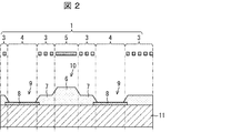
- 2 is a cross-sectional view along plane AA shown in FIG.
- the photomask 1 includes a plurality of openings 9 (openings) for depositing a light emitting material of an organic light emitting diode, and a plurality of photos for supporting a fine metal mask (not shown) for depositing the light emitting material. It is used for collectively forming the photosensitive organic layer 10 (edge cover) which consists of the spacer 6 (photo spacer part), and the flat part 7 which connects the photo spacer 6 and the opening 9.
- the photosensitive organic layer 10 is formed of polyimide resin, acrylic resin, epoxy resin or the like. Then, the photo spacer 6, the flat portion 7 and the opening 9 are formed in the photosensitive organic layer 10. The opening 9 exposes the anode electrode 8 (first electrode), and the end of the anode electrode 8 is covered with the flat portion 7.
- an island-like light emitting layer (not shown) covering the anode electrode 8 and a part of the photosensitive organic layer 10 deposits the light emitting material onto the anode electrode 8 and the photosensitive organic layer 10 by the evaporation method. It is formed by doing.
- a cathode electrode (second electrode) is formed on the light emitting layer.
- the photomask 1 has a plurality of strip patterns for forming a plurality of gray tone regions 2 (semi-transmissive portion, gray tone mask) in which a plurality of strip patterns 3 (fine patterns) are formed in parallel with one another.
- a plurality of aperture patterns 4 (transmissive portions) formed in the gray tone region 2 across 3 and a plurality of strip patterns 3 formed in the gray tone region 2 to form a plurality of photo spacers 6
- a plurality of light shielding patterns 5 light shielding portions.
- each of the plurality of opening patterns 4 is formed in a quadrilateral shape and arranged in a matrix.
- Each light shielding pattern 5 is disposed at a position surrounded by the four opening patterns 4 arranged in 2 rows and 2 columns.
- Each light shielding pattern 5 is formed in a cross shape so as to extend along the outer edge of each of the four opening patterns arranged in 2 rows and 2 columns, and an island shape is formed between the plurality of opening patterns 4 arranged in a grid. Is formed. The end of the light shielding pattern 5 sandwiched between the two opening patterns 4 is formed to extend along the outer edge of the opening pattern 4. The light shielding pattern 5 is formed so that its peripheral edge is in contact with the strip pattern 3.
- the opening 9 is formed by the opening pattern 4 of the photomask 1
- the photo spacer 6 is formed by the light shielding pattern 5
- the flat portion 7 is formed by the strip pattern 3.
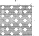
- FIG. 3 is a plan view schematically showing the configuration of a photomask 91 according to the comparative example.
- the photomask 91 is formed in a matrix in the gray tone region 2 across the plurality of strip patterns 3 to form the gray tone region 2 in which the plurality of strip patterns 3 are formed in parallel with each other and the plurality of openings 9.
- a plurality of light shielding patterns 95 formed in the gray tone region 2 across the plurality of strip patterns 3 to form the plurality of photo spacers 6.
- Each light shielding pattern 95 is formed in a circular shape at a position surrounded by four opening patterns 4 arranged in two rows and two columns.
- the light shielding patterns 5 are adjacent to each other along the outer edges of the four opening patterns 4 arranged in two rows and two columns. It is formed in the shape of a cross so as to fill the gap between and to extend. For this reason, the area of the light shielding pattern 5 is increased. Therefore, the volume of the photo spacer 6 formed by the light shielding pattern 5 is increased. As a result, regardless of the pattern density, a volume in which the height of the photo spacer 6 can be obtained is secured, and a reduction in the height of the photo spacer 6 due to the thermal sag is prevented.
- the light shielding pattern 95 corresponding to the photo spacer is circular, the present invention is not limited to this.
- the light shielding pattern 95 may have another shape that does not follow the opening pattern 4, such as a rectangle, a rhombus, or an ellipse.
- the light shielding pattern is arranged at a position surrounded by four opening patterns arranged in two rows and two columns, the present invention is not limited to this.
- the light shielding pattern may be disposed at a position surrounded by two or three opening patterns.
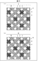
- FIG. 4A is a cross-sectional view of the substrate 11 and the photosensitive organic layer 90 according to the comparative example before firing
- FIG. 4B is a cross-sectional view of the substrate 11 and the photosensitive organic layer 90 according to the comparative example after firing
- FIG. 4C is a cross-sectional view of the substrate 11 and the photosensitive organic layer 10 according to the first embodiment before firing
- FIG. 4D is a substrate 11 and the photosensitive organic layer according to the first embodiment. It is sectional drawing after 10 baking.
- the photo spacer 96 and the edge cover 97 are formed on the photosensitive organic layer 90 on the substrate 11 by the photomask 91 shown in FIG. 3 as shown in FIG.
- the height H1 of the photo spacer 96 is such that a thermal sag occurs in the photo spacer 96 at the time of firing and the photo spacer 96 is deformed to have a height H2 smaller than the height H1 as shown in FIG. 4B. Phenomenon occurs.
- the volume of the photo spacer 6 formed by the light shielding pattern 5 is larger than the volume of the photo spacer 96 in FIG.
- the height H3 is higher than the height H2 of the comparative example.
- FIG. 5A is a plan view showing a modification of the photomask according to the first embodiment
- FIG. 5B is a plan view showing another modification.
- the same components as those described above are denoted by the same reference numerals. Detailed descriptions of these components will not be repeated.
- the photomasks 1A and 1B include gray tone areas 2 in which a plurality of strip patterns 3 are formed in parallel to one another.
- the direction in which the strip pattern 3 extends may be any direction, for example, a vertical direction as shown in FIG. 5 (a) or an oblique direction as shown in FIG. 5 (b).
- 6 (a) and 6 (b) are plan views showing still another modification of the photomask.
- the same components as those described above are denoted by the same reference numerals. Detailed descriptions of these components will not be repeated.
- the photomask 1C includes a gray tone area 2 composed of a pattern 3C such as a polka dot pattern.
- a pattern 3C such as a polka dot pattern.
- the band-like pattern 3 is formed in the gray tone area 2, but the present invention is not limited thereto.
- another pattern 3C such as a polka dot pattern or a checkered pattern may be formed.
- the photomask 1D includes a halftone region 2D formed of a halftone pattern 3D.
- a halftone area 2D may be provided instead of the gray tone area 2.
- FIGS. 7A and 7B are plan views showing still another modification of the photomask.
- the same components as those described above are denoted by the same reference numerals. Detailed descriptions of these components will not be repeated.
- a circular opening pattern 4E may be formed.
- a light shielding pattern 5E having a shape along the periphery of four circular opening patterns 4E in two rows and two columns is formed.
- the opening pattern may have another shape such as, for example, a rectangle, a rhombus, or an ellipse.
- each opening pattern may be different depending on the color (red (R), green (G), blue (B)) of the light emitting material of the organic light emitting diode formed in each opening 9, for example As shown in 7 (b), opening patterns 4F and 4FF having different shapes may be formed.
- FIG. 8 is a plan view showing still another modified example of the photomask.
- the same components as those described above are denoted by the same reference numerals. Detailed descriptions of these components will not be repeated.
- the flat portion 7 is provided between the opening 9 and the photo spacer 6, but the present invention is not limited to this.
- the flat portion 7 may not be provided.
- the light shielding pattern 5G is formed in close contact with a part of the periphery of each opening pattern 4 as shown in FIG.
- the positive photosensitive organic layer 10 is described in which the solubility in the developer increases and the exposed portion is removed when exposed to light, the solubility in the developer is increased when exposed to the contrary. It may be a negative photosensitive organic layer which decreases and leaves exposed portions after development. In the case of the negative type, the transmitting portion forms a photo spacer portion, the semi-transmitting light portion forms a planarizing portion, and the light shielding portion forms an opening. Further, although the example in which the edge cover is formed of the photosensitive organic layer has been described above, the organic layer may be patterned separately using a resist without using the photosensitive organic layer.
- the photomask according to the aspect 1 includes a plurality of first electrodes, an edge cover covering an end portion of the first electrode, an island-like light emitting layer covering the first electrode and a part of the edge cover, and a second And a photo mask for collectively forming the edge cover, wherein the edge cover has an opening for opening the first electrode, a flat portion, and the like. And a plurality of photo spacer portions higher than the flat portion, wherein the photomask forms a transmitting portion forming the opening, a semi-transmissive portion forming the flat portion, and the photo spacer portion.
- a light shielding portion wherein the light shielding portion is formed in an island shape between the plurality of transmission portions arranged in a grid, and an end portion of the light shielding portion sandwiched between the two transmission portions is an outer edge of the transmission portion It is formed to extend along the
- the transmission part is formed in a quadrilateral shape.
- the semi-transmissive light portion has a pattern in which a plurality of strip patterns are formed in parallel to one another.
- the light shielding portion is formed such that the peripheral edge thereof is in contact with the semi-transmission light portion.
- the light shielding portion is formed such that a part of the periphery thereof is in contact with the transmission portion.
- the semi-transmissive portion is formed by a halftone mask.
- the semi-transmissive portion is formed by a gray tone mask provided with a fine pattern.
- the display device is a display device including an edge cover that covers ends of a plurality of first electrodes, wherein the edge cover has an opening for opening the first electrode, a flat portion, and the flat portion. And an island-like light emitting layer covering the first electrode and a part of the edge cover, and the first electrode above the light emitting layer.
- the photo spacer portion is formed in an island shape between the plurality of openings arranged in a grid, and the end portion of the photo spacer portion sandwiched between the two openings Are formed to extend along the outer edge of the opening.
- a method of manufacturing a display device is a method of manufacturing a display device using the photomask according to the first aspect, comprising the steps of: forming the edge cover on a substrate; And a step of irradiating the edge cover with light through the photomask to form the photo spacer portion along the outer edge of the opening.
- the display according to the present embodiment is not particularly limited as long as it is a display panel provided with a display element.
- the above-mentioned display element is a display element whose luminance and transmittance are controlled by a current, and an organic EL (Electro Luminescence: electro luminescence) provided with an OLED (Organic Light Emitting Diode) as a display element of current control.
- An EL display such as an inorganic EL display including a display or an inorganic light emitting diode, and a QLED display including a quantum dot light emitting diode (QLED).
- Photo mask 2 Gray tone area (translucent light, gray tone mask) 3 band pattern (fine pattern) 4 Opening pattern (transmission part) 5 Shading pattern (shading part) 6 Photo Spacer (Photo Spacer) 7 Flat portion 8 Anode electrode (first electrode) 9 opening (opening) 10 Photosensitive organic layer (edge cover)
Landscapes
- Physics & Mathematics (AREA)
- General Physics & Mathematics (AREA)
- Engineering & Computer Science (AREA)
- Manufacturing & Machinery (AREA)
- Microelectronics & Electronic Packaging (AREA)
- Electroluminescent Light Sources (AREA)
Abstract
フォトマスク(1)は、前記開口部を形成する透過部と、前記平坦部を形成する半透過光部と、前記フォトスペーサ部を形成する遮光部と、を備え、 前記遮光部は格子状に並ぶ複数の前記透過部の間に島状に形成され、 2つの前記透過部に挟まれた前記遮光部の端部は前記透過部の外縁に沿って延伸するように形成される
Description
本発明は、フォトマスク、それを用いた表示装置及び表示装置の製造方法に関する。
有機発光ダイオードの陽極電極(下部電極)の周縁を覆うエッジカバー(絶縁膜)と、上記陽極電極上に形成され、上記発光材料を蒸着するためのファインメタルマスクのスペーサとして機能するフォトスペーサ(リブ)とを備える表示装置が知られている(特許文献1)。
上記エッジカバーは、陽極電極の周縁を覆う状態で形成され、このエッジカバーに形成された窓から陽極電極が露出する。その後、このエッジカバー上にフォトスペーサが形成される。
上記エッジカバーと上記フォトスペーサとをグレートーンパターンを備えたフォトマスクを用いて一括形成すると、2回の露光工程が1回の露光工程で済むため有利である。
しかしながら、複数の小さなフォトスペーサを形成する場合、焼成時に熱ダレが発生してフォトスペーサが変形し、フォトスペーサの高さが低くなってしまうという現象が生じる。この現象は高精細の表示装置において特に問題になる。
本発明の一態様に係るフォトマスクは、複数の第1電極と、前記第1電極の端部を覆うエッジカバーと、前記第1電極と前記エッジカバーの一部とを覆う島状の発光層と、第2電極と、を備える表示装置を形成するためのフォトマスクのうち、前記エッジカバーを一括形成するためのフォトマスクであって、前記エッジカバーは、前記第1電極を開口する開口部、平坦部、及び前記平坦部よりも高い複数のフォトスペーサ部、を備え、前記フォトマスクは、前記開口部を形成する透過部と、前記平坦部を形成する半透過光部と、前記フォトスペーサ部を形成する遮光部と、を備え、前記遮光部は格子状に並ぶ複数の前記透過部の間に島状に形成され、2つの前記透過部に挟まれた前記遮光部の端部は前記透過部の外縁に沿って延伸するように形成される。
本発明の一態様によれば、焼成時の熱ダレによるフォトスペーサの高さの低下を防止することができる。
以下、本発明の実施形態を説明する。
図1は実施形態1に係るフォトマスク1の構成を模式的に示す平面図である。図2は図1に示される面AAに沿った断面図である。
フォトマスク1は、有機発光ダイオードの発光材料を蒸着するための複数の開口9(開口部)と、この発光材料を蒸着するためのファインメタルマスク(図示せず)を支持するための複数のフォトスペーサ6(フォトスペーサ部)と、フォトスペーサ6と開口9とをつなぐ平坦部7からなる感光性有機層10(エッジカバー)を一括形成するために使用される。
感光性有機層10は、ポリイミド樹脂、アクリル樹脂、エポキシ樹脂などから形成される。そして、感光性有機層10にフォトスペーサ6、平坦部7及び開口9が形成される。上記開口9は、陽極電極8(第1電極)を露出し、陽極電極8の端部は平坦部7で覆われる。
そして、陽極電極8と感光性有機層10の一部とを覆う島状の発光層(図示せず)が、蒸着法によって、陽極電極8と感光性有機層10上に、上記発光材料を蒸着することにより形成される。この発光層の上に陰極電極(第2電極)が形成される。
フォトマスク1は、複数の帯状パターン3(微細パターン)が互いに平行に形成されるグレートーン領域2(半透過光部、グレイトーンマスク)と、複数の開口9を形成するために複数の帯状パターン3を跨いでグレートーン領域2内に形成される複数の開口パターン4(透過部)と、複数のフォトスペーサ6を形成するために複数の帯状パターン3を跨いでグレートーン領域2内に形成される複数の遮光パターン5(遮光部)とを備える。図1に示す例では、複数の開口パターン4のそれぞれが、四辺形状に形成され、マトリックス状に配置される。そして、各遮光パターン5が、2行2列に配置された4個の開口パターン4により囲まれる位置に配置される。
各遮光パターン5は、2行2列に配置された4個の開口パターンのそれぞれの外縁に沿って延伸するように十字状に形成され、格子状に並ぶ複数の開口パターン4の間に島状に形成される。2つの開口パターン4に挟まれた遮光パターン5の端部は、開口パターン4の外縁に沿って延伸するように形成される。遮光パターン5は、その周縁が帯状パターン3と接するように形成される。
フォトマスク1の開口パターン4により開口9が形成され、遮光パターン5によりフォトスペーサ6が形成され、帯状パターン3により平坦部7が形成される。
図3は比較例に係るフォトマスク91の構成を模式的に示す平面図である。フォトマスク91は、複数の帯状パターン3が互いに平行に形成されるグレートーン領域2と、複数の開口9を形成するために複数の帯状パターン3を跨いでグレートーン領域2内にマトリックス状に形成される四辺形状の複数の開口パターン4と、複数のフォトスペーサ6を形成するために複数の帯状パターン3を跨いでグレートーン領域2内に形成される複数の遮光パターン95とを備える。各遮光パターン95は、2行2列に配置された4個の開口パターン4により囲まれる位置に円形状に形成される。
このように、円形状の小さな遮光パターン95を形成する場合、遮光パターン95により形成されたフォトスペーサの焼成時にフォトスペーサに熱ダレが発生してフォトスペーサが変形し、フォトスペーサの高さが低くなってしまうという現象が生じる。この現象は高精細のOLEDパネルにおいて特に問題になる。
これに対して、本実施形態では、図1に示すように、遮光パターン5が、2行2列に配置された4個の開口パターン4のそれぞれの外縁に沿って、隣接する開口パターン4の間の隙間を埋めて延伸するように十字状に形成される。このため、遮光パターン5の面積が増大する。従って、遮光パターン5により形成されるフォトスペーサ6の体積が増大する。この結果、パターン密度に関わらず、フォトスペーサ6の高さが稼げる体積が確保され、熱ダレによるフォトスペーサ6の高さの低下が防止される。
なお、フォトスペーサに対応する遮光パターン95が円形である例を示しているが、本発明はこれに限定されない。遮光パターン95は開口パターン4に沿わない、例えば長方形、菱形、楕円等の他の形状でもよい。
また、2行2列に配置された4個の開口パターンにより囲まれる位置に遮光パターンが配置される例を示しているが、本発明はこれに限定されない。例えば、2個や3個の開口パターンにより囲まれる位置に遮光パターンが配置されでもよい。
図4(a)は比較例に係る基板11及び感光性有機層90の焼成前の断面図であり、図4(b)は比較例に係る基板11及び感光性有機層90の焼成後の断面図であり、図4(c)は実施形態1に係る基板11及び感光性有機層10の焼成前の断面図であり、図4(d)は実施形態1に係る基板11及び感光性有機層10の焼成後の断面図である。
図3に示されるフォトマスク91により、基板11上の感光性有機層90にフォトスペーサ96及びエッジカバー97が図4(a)に示すように形成される。フォトスペーサ96の高さH1は、焼成時にフォトスペーサ96に熱ダレが発生してフォトスペーサ96が変形し、図4(b)に示すように高さH1よりも低い高さH2になってしまうという現象が生じる。
これに対して、本実施形態では、遮光パターン5により形成されるフォトスペーサ6の体積が、図4(a)のフォトスペーサ96の体積よりも増大するので、フォトスペーサ6の高さは、焼成後、図4(d)に示すように、比較例の高さH2よりも高い高さH3となる。このように、熱ダレによるフォトスペーサ6の高さの低下が抑制される。
図5(a)は実施形態1に係るフォトマスクの変形例を示す平面図であり、図5(b)は他の変形例を示す平面図である。前述した構成要素と同様の構成要素には同様の参照符号を付している。これらの構成要素の詳細な説明は繰り返さない。
フォトマスク1A・1Bは、複数の帯状パターン3が互いに平行に形成されるグレートーン領域2を備える。前述した例では、帯状パターン3が水平方向に延伸する例を示したが、本発明はこれに限定されない。帯状パターン3が延伸する方向はどの方向でもよく、例えば、図5(a)に示すように垂直方向でもよく、図5(b)に示すように斜め方向でもよい。
図6(a)(b)は上記フォトマスクのさらに他の変形例を示す平面図である。前述した構成要素と同様の構成要素には同様の参照符号を付している。これらの構成要素の詳細な説明は繰り返さない。
フォトマスク1Cは、図6(a)に示すように、水玉模様等のパターン3Cからなるグレートーン領域2を備える。前述した例では、帯状パターン3がグレートーン領域2に形成される例を示したが、本発明はこれに限定されない。帯状パターン3の替わりに水玉模様、市松模様等の他のパターン3Cが形成されてもよい。
フォトマスク1Dは、図6(b)に示すように、ハーフトーンパターン3Dからなるハーフトーン領域2Dを備える。前述した例では、グレートーン領域2の例を示したが、本発明はこれに限定されない。グレートーン領域2の替わりにハーフトーン領域2Dを備えてもよい。
図7(a)(b)は上記フォトマスクのさらに他の変形例を示す平面図である。前述した構成要素と同様の構成要素には同様の参照符号を付している。これらの構成要素の詳細な説明は繰り返さない。
前述した例では、矩形の開口パターン4の例を示したが、本発明はこれに限定されない。矩形の開口パターン4の替わりに、図7(a)に示すように円形の開口パターン4Eを形成してもよい。この場合、2行2列の4個の円形の開口パターン4Eの周縁に沿った形状の遮光パターン5Eが形成される。開口パターンは例えば長方形、菱形、楕円等の他の形状でもよい。
また、各開口パターンの形状は、各開口9に形成する有機発光ダイオードの発光材料の色(赤色(R)、緑色(G)、青色(B))に応じて異なっていてもよく、例えば図7(b)に示すように、形状の異なる開口パターン4F・4FFを形成してもよい。
図8は上記フォトマスクのさらに他の変形例を示す平面図である。前述した構成要素と同様の構成要素には同様の参照符号を付している。これらの構成要素の詳細な説明は繰り返さない。
前述した例では、開口9とフォトスペーサ6との間に平坦部7が設けられる構成を示したが、本発明はこれに限定されない。平坦部7は設けられなくてもよい。この場合、遮光パターン5Gが、図8に示すように各開口パターン4の周縁の一部に密接するように形成される。
以上、露光されると現像液に対して溶解性が増大し、露光部が除去されるポジ型の感光性有機層10で説明したが、逆に露光されると現像液に対して溶解性が低下し、現像後に露光部分が残るネガ型の感光性有機層であってもよい。ネガ型の場合は、透過部はフォトスペーサ部を形成し、半透過光部が平坦化部を形成し、遮光部が開口部を形成する。また、上記はエッジカバーを感光性有機層で形成する例を説明したが、感光性の有機層を用いず、別途レジストを用いて有機層をパターニングしてもよい。
〔まとめ〕
態様1のフォトマスクは、複数の第1電極と、前記第1電極の端部を覆うエッジカバーと、前記第1電極と前記エッジカバーの一部とを覆う島状の発光層と、第2電極と、を備える表示装置を形成するためのフォトマスクのうち、前記エッジカバーを一括形成するためのフォトマスクであって、前記エッジカバーは、前記第1電極を開口する開口部、平坦部、及び前記平坦部よりも高い複数のフォトスペーサ部、を備え、前記フォトマスクは、前記開口部を形成する透過部と、前記平坦部を形成する半透過光部と、前記フォトスペーサ部を形成する遮光部と、を備え、前記遮光部は格子状に並ぶ複数の前記透過部の間に島状に形成され、2つの前記透過部に挟まれた前記遮光部の端部は前記透過部の外縁に沿って延伸するように形成される。
態様1のフォトマスクは、複数の第1電極と、前記第1電極の端部を覆うエッジカバーと、前記第1電極と前記エッジカバーの一部とを覆う島状の発光層と、第2電極と、を備える表示装置を形成するためのフォトマスクのうち、前記エッジカバーを一括形成するためのフォトマスクであって、前記エッジカバーは、前記第1電極を開口する開口部、平坦部、及び前記平坦部よりも高い複数のフォトスペーサ部、を備え、前記フォトマスクは、前記開口部を形成する透過部と、前記平坦部を形成する半透過光部と、前記フォトスペーサ部を形成する遮光部と、を備え、前記遮光部は格子状に並ぶ複数の前記透過部の間に島状に形成され、2つの前記透過部に挟まれた前記遮光部の端部は前記透過部の外縁に沿って延伸するように形成される。
態様2では、前記透過部が四辺形状に形成される。
態様3では、前記半透過光部は、複数の帯状パターンが互いに平行に形成されるパターンを有する。
態様4では、前記遮光部は、その周縁が前記半透過光部と接するように形成される。
態様5では、前記遮光部は、その周縁の一部が前記透過部と接するように形成される。
態様6では、前記半透過光部が、ハーフトーンマスクにより形成される。
態様7では、前記半透過光部が、微細パターンが設けられたグレイトーンマスクにより形成される。
態様8の表示装置は、複数の第1電極の端部を覆うエッジカバーを備える表示装置であって、前記エッジカバーが、前記第1電極を開口する開口部と、平坦部と、前記平坦部よりも高い複数のフォトスペーサ部と、を備え、前記表示装置が、前記第1電極と前記エッジカバーの一部とを覆う島状の発光層と、前記発光層よりも上層で前記第1電極に共通する第2電極と、をさらに備え、前記フォトスペーサ部は格子状に並ぶ複数の開口部の間に島状に形成され、2つの前記開口部に挟まれた前記フォトスペーサ部の端部は前記開口部の外縁に沿って延伸するように形成される。
態様9の表示装置の製造方法は、態様1に記載のフォトマスクを用いた表示装置の製造方法であって、基板上に前記エッジカバーを形成する工程と、前記エッジカバーの上に前記フォトマスクを載置する工程と、前記フォトマスクを通して前記エッジカバーに光を照射して、前記開口部の外縁に沿って前記フォトスペーサ部を形成する工程とを包含する。
本発明は上述した各実施形態に限定されるものではなく、請求項に示した範囲で種々の変更が可能であり、異なる実施形態にそれぞれ開示された技術的手段を適宜組み合わせて得られる実施形態についても本発明の技術的範囲に含まれる。さらに、各実施形態にそれぞれ開示された技術的手段を組み合わせることにより、新しい技術的特徴を形成することができる。
本実施形態に係るディスプレイは、表示素子を備えた表示パネルであれば、特に限定されるものではない。上記表示素子は、電流によって輝度や透過率が制御される表示素子であり、電流制御の表示素子としては、OLED(Organic Light Emitting Diode:有機発光ダイオード)を備えた有機EL(Electro Luminescence:エレクトロルミネッセンス)ディスプレイ、又は無機発光ダイオードを備えた無機ELディスプレイ等のELディスプレイQLED(Quantum dot Light Emitting Diode:量子ドット発光ダイオード)を備えたQLEDディスプレイ等がある。
1 フォトマスク
2 グレートーン領域(半透過光部、グレイトーンマスク)
3 帯状パターン(微細パターン)
4 開口パターン(透過部)
5 遮光パターン(遮光部)
6 フォトスペーサ(フォトスペーサ部)
7 平坦部
8 陽極電極(第1電極)
9 開口(開口部)
10 感光性有機層(エッジカバー)
2 グレートーン領域(半透過光部、グレイトーンマスク)
3 帯状パターン(微細パターン)
4 開口パターン(透過部)
5 遮光パターン(遮光部)
6 フォトスペーサ(フォトスペーサ部)
7 平坦部
8 陽極電極(第1電極)
9 開口(開口部)
10 感光性有機層(エッジカバー)
Claims (9)
- 複数の第1電極と、前記第1電極の端部を覆うエッジカバーと、前記第1電極と前記エッジカバーの一部とを覆う島状の発光層と、第2電極と、を備える表示装置を形成するためのフォトマスクのうち、前記エッジカバーを一括形成するためのフォトマスクであって、
前記エッジカバーは、前記第1電極を開口する開口部、平坦部、及び前記平坦部よりも高い複数のフォトスペーサ部、を備え、
前記フォトマスクは、前記開口部を形成する透過部と、前記平坦部を形成する半透過光部と、前記フォトスペーサ部を形成する遮光部と、を備え、
前記遮光部は格子状に並ぶ複数の前記透過部の間に島状に形成され、
2つの前記透過部に挟まれた前記遮光部の端部は前記透過部の外縁に沿って延伸するように形成されるフォトマスク。 - 前記透過部が四辺形状に形成される請求項1に記載のフォトマスク。
- 前記半透過光部は、複数の帯状パターンが互いに平行に形成されるパターンを有する請求項1に記載のフォトマスク。
- 前記遮光部は、その周縁が前記半透過光部と接するように形成される請求項1に記載のフォトマスク。
- 前記遮光部は、その周縁の一部が前記透過部と接するように形成される請求項1に記載のフォトマスク。
- 前記半透過光部が、ハーフトーンマスクにより形成される請求項1に記載のフォトマスク。
- 前記半透過光部が、微細パターンが設けられたグレイトーンマスクにより形成される請求項1に記載のフォトマスク。
- 複数の第1電極の端部を覆うエッジカバーを備える表示装置であって、
前記エッジカバーが、
前記第1電極を開口する開口部と、
平坦部と、
前記平坦部よりも高い複数のフォトスペーサ部と、を備え、
前記表示装置が、
前記第1電極と前記エッジカバーの一部とを覆う島状の発光層と、
前記発光層よりも上層で前記第1電極に共通する第2電極と、をさらに備え、
前記フォトスペーサ部は格子状に並ぶ複数の開口部の間に島状に形成され、2つの前記開口部に挟まれた前記フォトスペーサ部の端部は前記開口部の外縁に沿って延伸するように形成される表示装置。 - 請求項1に記載のフォトマスクを用いた表示装置の製造方法であって、
基板上に前記エッジカバーを形成する工程と、
前記エッジカバーの上に前記フォトマスクを載置する工程と、
前記フォトマスクを通して前記エッジカバーに光を照射して、前記開口部の外縁に沿って前記フォトスペーサ部を形成する工程とを包含する表示装置の製造方法。
Priority Applications (3)
| Application Number | Priority Date | Filing Date | Title |
|---|---|---|---|
| CN201780095416.8A CN111149055A (zh) | 2017-09-29 | 2017-09-29 | 光掩膜、显示装置以及显示装置的制造方法 |
| PCT/JP2017/035705 WO2019064573A1 (ja) | 2017-09-29 | 2017-09-29 | フォトマスク、表示装置及び表示装置の製造方法 |
| US16/471,591 US20190319222A1 (en) | 2017-09-29 | 2017-09-29 | Photomask and method for manufacturing display device |
Applications Claiming Priority (1)
| Application Number | Priority Date | Filing Date | Title |
|---|---|---|---|
| PCT/JP2017/035705 WO2019064573A1 (ja) | 2017-09-29 | 2017-09-29 | フォトマスク、表示装置及び表示装置の製造方法 |
Publications (1)
| Publication Number | Publication Date |
|---|---|
| WO2019064573A1 true WO2019064573A1 (ja) | 2019-04-04 |
Family
ID=65900936
Family Applications (1)
| Application Number | Title | Priority Date | Filing Date |
|---|---|---|---|
| PCT/JP2017/035705 Ceased WO2019064573A1 (ja) | 2017-09-29 | 2017-09-29 | フォトマスク、表示装置及び表示装置の製造方法 |
Country Status (3)
| Country | Link |
|---|---|
| US (1) | US20190319222A1 (ja) |
| CN (1) | CN111149055A (ja) |
| WO (1) | WO2019064573A1 (ja) |
Families Citing this family (2)
| Publication number | Priority date | Publication date | Assignee | Title |
|---|---|---|---|---|
| US11864452B1 (en) * | 2021-08-24 | 2024-01-02 | Apple Inc. | Black masking layer in displays having transparent openings |
| US12175907B2 (en) | 2022-12-09 | 2024-12-24 | Apple Inc. | Display with a transmitter under an active area |
Citations (4)
| Publication number | Priority date | Publication date | Assignee | Title |
|---|---|---|---|---|
| JP2003257650A (ja) * | 2002-03-05 | 2003-09-12 | Sanyo Electric Co Ltd | 有機エレクトロルミネッセンスパネルの製造方法、有機エレクトロルミネッセンス素子およびマスク |
| JP2011014504A (ja) * | 2009-07-06 | 2011-01-20 | Sharp Corp | 有機el表示装置およびその製造方法 |
| JP2011233341A (ja) * | 2010-04-27 | 2011-11-17 | Nec Lighting Ltd | 有機エレクトロルミネッセンス照明装置の製造方法 |
| WO2012053402A1 (ja) * | 2010-10-19 | 2012-04-26 | シャープ株式会社 | 蒸着装置、蒸着方法、並びに、有機エレクトロルミネッセンス表示装置の製造方法 |
Family Cites Families (5)
| Publication number | Priority date | Publication date | Assignee | Title |
|---|---|---|---|---|
| KR102030799B1 (ko) * | 2013-03-11 | 2019-10-11 | 삼성디스플레이 주식회사 | 유기발광표시장치 |
| KR101485166B1 (ko) * | 2013-04-25 | 2015-01-22 | 삼성디스플레이 주식회사 | 유기 발광 표시 장치 및 마스크 유닛 |
| KR102103499B1 (ko) * | 2013-10-16 | 2020-04-23 | 삼성디스플레이 주식회사 | 유기 발광 표시 장치 |
| KR102205401B1 (ko) * | 2014-01-14 | 2021-01-21 | 삼성디스플레이 주식회사 | 유기발광표시장치 |
| KR102414593B1 (ko) * | 2015-12-30 | 2022-06-30 | 엘지디스플레이 주식회사 | 유기 발광 표시 장치 및 이의 제조 방법 |
-
2017
- 2017-09-29 CN CN201780095416.8A patent/CN111149055A/zh active Pending
- 2017-09-29 WO PCT/JP2017/035705 patent/WO2019064573A1/ja not_active Ceased
- 2017-09-29 US US16/471,591 patent/US20190319222A1/en not_active Abandoned
Patent Citations (4)
| Publication number | Priority date | Publication date | Assignee | Title |
|---|---|---|---|---|
| JP2003257650A (ja) * | 2002-03-05 | 2003-09-12 | Sanyo Electric Co Ltd | 有機エレクトロルミネッセンスパネルの製造方法、有機エレクトロルミネッセンス素子およびマスク |
| JP2011014504A (ja) * | 2009-07-06 | 2011-01-20 | Sharp Corp | 有機el表示装置およびその製造方法 |
| JP2011233341A (ja) * | 2010-04-27 | 2011-11-17 | Nec Lighting Ltd | 有機エレクトロルミネッセンス照明装置の製造方法 |
| WO2012053402A1 (ja) * | 2010-10-19 | 2012-04-26 | シャープ株式会社 | 蒸着装置、蒸着方法、並びに、有機エレクトロルミネッセンス表示装置の製造方法 |
Also Published As
| Publication number | Publication date |
|---|---|
| US20190319222A1 (en) | 2019-10-17 |
| CN111149055A (zh) | 2020-05-12 |
Similar Documents
| Publication | Publication Date | Title |
|---|---|---|
| JP6680565B2 (ja) | 表示装置、及び、表示装置の製造方法 | |
| CN111326636B (zh) | 一种阵列基板、其制作方法、显示面板及显示装置 | |
| US10205121B2 (en) | Organic electroluminescent display panel and display apparatus | |
| CN105826355B (zh) | 一种显示面板的制作方法 | |
| CN111148861B (zh) | 蒸镀掩模及蒸镀掩模的制造方法 | |
| JP6980645B2 (ja) | Oledディスプレイ基板、oledディスプレイ装置およびoledディスプレイ基板の製造方法 | |
| CN111081745A (zh) | 显示面板及其制备方法 | |
| CN110277434B (zh) | 一种有机电致发光显示面板及显示装置 | |
| WO2015196613A1 (zh) | 彩膜基板及其制造方法、显示面板 | |
| WO2015014072A1 (zh) | 一种电致发光显示屏及其制备方法、显示装置 | |
| CN108346685B (zh) | 一种阵列基板及其制备方法、显示装置 | |
| WO2017107439A1 (zh) | 彩膜基板及其制作方法、显示装置 | |
| CN111900263A (zh) | 有机发光显示面板及其制作方法、显示装置 | |
| WO2019064419A1 (ja) | 蒸着マスク及び蒸着マスクの製造方法 | |
| CN104865729A (zh) | 彩膜基板及其制作方法、隔垫物的制作方法及显示装置 | |
| WO2010098093A1 (ja) | カラーフィルタ及びカラーフィルタの製造方法 | |
| TWI463659B (zh) | 薄膜電晶體陣列及其製造方法 | |
| US11476451B2 (en) | Display device and manufacturing method thereof for reducing color cast between view angles | |
| WO2019064573A1 (ja) | フォトマスク、表示装置及び表示装置の製造方法 | |
| WO2022022072A1 (zh) | 显示基板、显示面板及显示装置 | |
| JP5549233B2 (ja) | カラーフィルタ基板の露光方法 | |
| CN106773417B (zh) | 显示装置 | |
| JP5542456B2 (ja) | カラーフィルタ基板の露光方法 | |
| WO2014030581A1 (ja) | カラーフィルタ基板、及び、その製造方法 | |
| CN115315811B (zh) | 显示面板及其制备方法、显示装置 |
Legal Events
| Date | Code | Title | Description |
|---|---|---|---|
| 121 | Ep: the epo has been informed by wipo that ep was designated in this application |
Ref document number: 17927511 Country of ref document: EP Kind code of ref document: A1 |
|
| NENP | Non-entry into the national phase |
Ref country code: DE |
|
| 122 | Ep: pct application non-entry in european phase |
Ref document number: 17927511 Country of ref document: EP Kind code of ref document: A1 |
|
| NENP | Non-entry into the national phase |
Ref country code: JP |