WO2019064341A1 - 補修機能付き塗布装置および部品実装システム - Google Patents
補修機能付き塗布装置および部品実装システム Download PDFInfo
- Publication number
- WO2019064341A1 WO2019064341A1 PCT/JP2017/034735 JP2017034735W WO2019064341A1 WO 2019064341 A1 WO2019064341 A1 WO 2019064341A1 JP 2017034735 W JP2017034735 W JP 2017034735W WO 2019064341 A1 WO2019064341 A1 WO 2019064341A1
- Authority
- WO
- WIPO (PCT)
- Prior art keywords
- substrate
- liquid material
- solder
- unit
- repair
- Prior art date
- Legal status (The legal status is an assumption and is not a legal conclusion. Google has not performed a legal analysis and makes no representation as to the accuracy of the status listed.)
- Ceased
Links
Images







Classifications
-
- H—ELECTRICITY
- H05—ELECTRIC TECHNIQUES NOT OTHERWISE PROVIDED FOR
- H05K—PRINTED CIRCUITS; CASINGS OR CONSTRUCTIONAL DETAILS OF ELECTRIC APPARATUS; MANUFACTURE OF ASSEMBLAGES OF ELECTRICAL COMPONENTS
- H05K3/00—Apparatus or processes for manufacturing printed circuits
- H05K3/30—Assembling printed circuits with electric components, e.g. with resistors
- H05K3/32—Assembling printed circuits with electric components, e.g. with resistors electrically connecting electric components or wires to printed circuits
- H05K3/34—Assembling printed circuits with electric components, e.g. with resistors electrically connecting electric components or wires to printed circuits by soldering
Definitions
- the present invention relates to a coating device with repair function and a component mounting system, and more particularly to a coating device with repair function and a component mounting system including a coating unit that applies a liquid material to a substrate.
- a coating device with a repair function provided with a coating unit for coating a liquid material onto a substrate, for example, cream solder (liquid material) on lands (predetermined places) of the substrate disclosed in JP-A-8-204399.
- a mounted substrate production system component mounting system
- cream solder printer for printing.
- the inspection of the state of the cream solder printed on the land of the substrate by the machine and the confirmation of the inspection result of the machine inspection by the operator are performed. ing. Then, when the solder inspection machine determines that the state of the cream solder on the substrate based on the mechanical inspection and the inspection determination is defective, it notifies the operator of a repair instruction to repair the solder on the substrate. It is configured. In addition, the solder inspection machine is configured to interrupt (stop) work on another substrate until work for a manual failure by the operator is performed based on the repair instruction.
- the present invention has been made to solve the problems as described above, and one object of the present invention is to suppress a significant decrease in production efficiency even when a substrate requiring repair is generated. It is an object of the present invention to provide an application device and a component mounting system with a good
- the controller is also provided with a control unit that performs control to apply and repair the liquid material by the application unit even when there is a shortage.
- the application part applies the liquid material. It has a control unit that performs control to repair and repair. As a result, since the repair is automatically performed without waiting for the operator's operation for the defect manually, the production can be continued without stopping the production. As a result, when a substrate requiring repair is generated, it is possible to suppress a large decrease in production efficiency.
- control unit preferably applies the coating unit based on the shortage amount of the liquid material acquired by the inspection of the liquid material applied or printed on a predetermined location on the substrate. Control is performed to apply and repair the liquid material.
- an amount based on the insufficient amount of the liquid material can be applied to a predetermined location on the substrate for repair, so that an appropriate amount of liquid material is applied to the predetermined location on the substrate for repair. be able to.
- the control unit causes the application unit to perform the process based on the shortage position of the liquid material and the shortage amount of the liquid material obtained by the inspection of the liquid material applied or printed at a predetermined location on the substrate. It is configured to perform control to repair an insufficient position at a predetermined location.
- an amount based on the shortage of the liquid material can be applied to the shortage position of the liquid material at a predetermined location on the substrate to be repaired, so that an appropriate position at the predetermined location on the substrate can be appropriately corrected.
- An amount of liquid material can be applied. As a result, repair can be performed more appropriately.
- the coating unit further includes an inspection unit that inspects a liquid material applied or printed on a predetermined place on the substrate;
- the inspection of the liquid material is performed, and the application section performs control to apply and repair the liquid material.
- the inspection of the liquid material applied to the predetermined place and the repair of the liquid material on the predetermined place on the substrate can be performed in the same coating apparatus, so that the repair by the application part of the predetermined place can be performed quickly. It can be carried out.
- the coating unit includes a nozzle from which the liquid material is discharged, and the control unit is an insufficient amount of the liquid material coated or printed at a predetermined location on the substrate.
- control is performed to adjust the clearance between the tip of the nozzle and the substrate.
- the tip of the nozzle does not contact the substrate due to the clearance (gap) between the tip of the nozzle and the substrate, so application or printing is performed on a predetermined location on the substrate by contact with the tip of the nozzle.
- the deformation of the shape of the liquid material can be suppressed.
- the clearance between the tip of the nozzle and the substrate is adjusted in accordance with the shortage amount of the liquid material, it is possible to more appropriately repair the predetermined portion on the substrate.
- the inspection unit includes a volume measurement unit capable of measuring the volume of the liquid material
- the control unit is a liquid measured by the volume measurement unit. It is configured to acquire the shortage of liquid material based on the volume of the material. With this configuration, it is possible to accurately acquire the amount of liquid material applied or printed at a predetermined location. Therefore, the insufficient amount can be accurately acquired to obtain an appropriate amount of liquid material at a predetermined location on the substrate. It can be applied.
- the application unit for applying the liquid material to the substrate and the application unit when the amount of the liquid material applied or printed at a predetermined location on the substrate is insufficient An application device with a repair function that includes a control unit that performs control to apply and repair a liquid material, and a component that is disposed downstream of the application device with a repair function and that mounts components on a substrate carried out of the application device with a repair function. And a mounting device.
- the component mounting system includes the application device with a repair function including a control unit that performs control to apply and repair the liquid material by the application unit.
- FIG. 1 is a schematic block diagram showing a configuration of a component mounting system according to a first embodiment of the present invention.
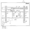
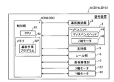
- FIG. 1 is a schematic plan view showing the entire configuration of a coating apparatus according to a first embodiment of the present invention. It is a typical side view showing composition of a coating device by a 1st embodiment of the present invention. It is a typical block diagram showing the control composition of the coating device by the 1st, 2nd embodiment and the 1st modification of the present invention. It is the elements on larger scale which showed the state which test
- FIG. 12A is a schematic view showing a state in which the clearance between the tip of the nozzle and the substrate is large.
- FIG. 12B is a schematic view showing a state where the clearance between the tip of the nozzle and the substrate is small.
- the component mounting system 1 of 1st Embodiment is provided with the printing apparatus 1a, the coating device 1b, and the component mounting apparatus 1c, as shown in FIG.
- the printing device 1a, the coating device 1b, and the component mounting device 1c are arranged in this order from the upstream side.
- the coating device 1 b is an example of the “coating device with repair function” in the claims.
- the printing apparatus 1a is configured to print the solder S on a predetermined location RA on the substrate B by printing the solder S (cream solder) (see FIG. 5) on the substrate B based on a predetermined pattern.
- the predetermined place RA is a place on the substrate B where the solder S is printed.
- a general printing apparatus is suitably used for the printing apparatus 1a.
- the solder S is an example of the “liquid material” in the claims.
- the component mounting apparatus 1c is configured to mount an electronic component on the substrate B carried out of the coating apparatus 1b.
- a general component mounting apparatus is suitably used for the component mounting apparatus 1c.
- the electronic component is a component such as an IC, a transistor, a capacitor, and a resistor.
- the coating device 1 b will be described below.
- the solder by the dispense head 41 it is comprised so that control which newly apply
- the application of the solder S by the dispense head 41 is a broad concept including the spreading of the solder S on the substrate B, the discharge of the solder S on the substrate B, and the ejection of the solder S on the substrate B.
- the dispense head 41 is an example of the “applying section” in the claims.
- the coating apparatus 1 b includes a base 2, a substrate conveyance unit 3, a head unit 4, a support unit 5, a pair of rail units 6, and a substrate imaging unit 7. , And the control unit 8.
- the direction in which the substrate B is transported by the pair of conveyors is taken as the X direction
- the direction perpendicular to the X direction in the horizontal direction is taken as the Y direction
- a direction perpendicular to the X direction and the Y direction is taken as a Z direction (vertical direction).
- the board imaging unit 7 is an example of the “inspection unit” in the claims.
- the base 2 is a base on which the respective components are arranged in the coating apparatus 1 b.
- a substrate transfer unit 3 and a rail unit 6 are provided on the base 2 as respective components.
- a control unit 8 is provided in the base 2.
- the substrate transport unit 3 is configured to carry in the substrate B from the outside of the coating device 1 b and transport the substrate B in the transport direction (direction X1).
- the substrate transport unit 3 includes a pair of conveyor units 30 and a drive motor 32.
- Each of the pair of conveyor units 30 has a pulley (not shown) and a ring-shaped conveyor belt 31 wound around the pulley.
- the control unit 8 is configured to control the transport speed of the substrate B placed on the transport belt 31 by controlling the drive motor 32.
- the head unit 4 is a head unit 4 for applying a solder, and is configured to apply a solder S to a substrate B fixed at a predetermined position.
- the head unit 4 includes the dispense head 41.
- Dispensing head 41 is connected to a syringe (not shown) filled with solder S so that solder S supplied from the syringe can be applied onto substrate B from the tip of nozzle 41a (see FIG. 3) It is done.
- the dispensing head 41 is configured to be movable in the vertical direction by a Z-axis motor 42 (see FIG. 4).
- the support portion 5 is configured to support the head unit 4 so as to be movable in the transport direction (X1 direction) and in the direction (X2 direction) opposite to the transport direction.
- the support portion 5 includes a ball screw shaft 51 extending in the transport direction, and an X-axis motor 52 that rotates the ball screw shaft 51.
- the head unit 4 is provided with a ball nut (not shown) engaged with the ball screw shaft 51 of the support portion 5.
- the head unit 4 is configured to be movable in the transport direction along the support portion 5 together with the ball nut engaged with the ball screw shaft 51 by the rotation of the ball screw shaft 51 by the X-axis motor 52.
- the pair of rail portions 6 is configured to support the support portion 5 so as to be movable in the Y direction.
- the rail portion 6 includes a ball screw shaft 61 extending in the Y direction, and a Y axis motor 62 for rotating the ball screw shaft 61.
- the support portion 5 is provided with a ball nut (not shown) engaged with the ball screw shaft 61 of the rail portion 6.
- the support portion 5 is configured to be movable in the Y direction along the pair of rail portions 6 together with the ball nut engaged with the ball screw shaft 61 by rotating the ball screw shaft 61 by the Y-axis motor 62 There is.
- the head unit 4 is configured to be movable on the base 2 in the horizontal plane (in the X direction and in the Y direction). That is, the head unit 4 is configured to be movable relative to the substrate B on the substrate transport unit 3. As a result, the head unit 4 can move to the upper side of the substrate B fixed at the predetermined position, and apply the solder S supplied from the dispense head 41 on the substrate B.
- the board imaging unit 7 is attached to the head unit 4 as shown in FIG. It is a camera for mark recognition which takes an image of).
- the FI mark is a mark for confirming the position of the substrate B.
- the substrate imaging unit 7 is a camera for a solder inspection which picks up the solder S printed on a predetermined place RA on the substrate B.
- the substrate imaging unit 7 captures a two-dimensional (plan view) image of the solder S printed on the substrate B.
- control unit 8 is a control circuit that includes a CPU 81 (Central Processing Unit), a memory 82 and the like, and controls the operation of the coating device 1 b.
- the control unit 8 is electrically connected to the substrate conveyance unit 3, the head unit 4, the support unit 5, the rail unit 6, the substrate imaging unit 7, the X-axis motor 52, and the Y-axis motor 62.
- the memory 82 is a substrate including a work of applying the solder S by the dispense head 41 and repairing it based on the shortage amount SQ of the solder S obtained by inspection of the solder S printed on the predetermined place RA on the substrate B
- a substrate work program BP based on work processing is stored.
- the control unit 8 controls the head unit 4, the support unit 5, the rail unit 6, the substrate imaging unit 7, the X-axis motor 52 and the Y-axis motor 62 according to the substrate work program BP to print on a predetermined place RA.
- the solder S is configured to be repaired.
- the control unit 8 is configured to perform imaging of the solder S by the substrate imaging unit 7 and control to apply and repair the solder S by the dispensing head 41. Specifically, the control unit 8 is based on the shortage position SP of the solder S and the shortage amount SQ of the solder S at the shortage position SP acquired by the imaging result of the solder S printed at the predetermined location RA on the substrate B
- the dispensing head 41 is configured to perform control to repair the shortage position SP at the predetermined location RA.
- the control unit 8 flattens the solder S
- the shape CS two-dimensional shape CS
- FIG. 6 when the position of the FI mark on the substrate B is the reference position, the control unit 8 of the coating device 1b is applied to the third predetermined position RA from one side (X2 side) Acquire the reference shape DS of the solder S.
- the control unit 8 determines whether the inspection result of the solder S at the predetermined place RA is good or bad based on the comparison between the reference shape DS of the solder S and the shape CS of the solder S.
- the control unit 8 of the coating device 1b determines the position (first insufficient position SP1) in the plane (in the XY plane) of the first insufficient portion R1 based on the reference shape DS of the solder S. Get). Further, based on the reference shape DS of the solder S, the control unit 8 of the coating device 1b acquires the position (second insufficient position SP2) in the plane (in the XY plane) of the second insufficient portion R2.
- the first shortage position SP1 and the second shortage position SP2 are examples of the “missing position” in the claims.
- the control unit 8 of the coating device 1b acquires the ratio of the first insufficient portion R1 to the reference shape DS of the solder S. Thereby, the control unit 8 of the coating device 1 b is based on the amount of the solder S necessary to form the reference shape DS of the solder S and the ratio of the first insufficient portion R1 to the reference shape DS of the solder S.
- the amount of the solder S applied to the first shortage R1 (first shortage SQ1) is acquired.
- the first shortage amount SQ1 is an example of the “lack amount” in the claims.
- control unit 8 of the coating device 1b acquires the ratio of the second insufficient portion R2 to the reference shape DS of the solder S.
- the control unit 8 of the coating apparatus 1b determines the amount of the solder S necessary to form the reference shape DS of the solder S and the ratio of the second insufficient portion R2 to the reference shape DS of the solder S.
- the amount of the solder S applied to the second shortage R2 (second shortage SQ2) is acquired.
- the second shortage SQ2 is an example of the "shortage" in the claims.
- the control unit 8 of the coating apparatus 1b applies the solder S to the first shortage portion R1 by the dispense head 41 based on the first shortage position SP1 and the first shortage amount SQ1. Furthermore, the control unit 8 of the coating device 1b applies the solder S to the second shortage portion R2 by the dispense head 41 based on the second shortage position SP2 and the second shortage amount SQ2.
- the repair location at the predetermined location RA where the solder S is applied is repaired.
- the repair of the repair location at the predetermined location RA is performed by applying (dotting) the solder S from the dispense head 41 so as to have a substantially circular shape in plan view.
- step S ⁇ b> 1 the control unit 8 inspects the solder S at a predetermined place RA on the substrate B printed by the printing apparatus 1 a. That is, the control unit 8 recognizes the solder S on the substrate B by the imaging of the substrate imaging unit 7 and compares the imaging result of the solder S on the substrate B with the reference shape DS to obtain the solder S on the substrate B To check.
- step S2 the control unit 8 determines whether the inspection result of the solder S on the substrate B is good. When the inspection of the solder S on the substrate B is defective, the control unit 8 proceeds to step S3. When the inspection of the solder S on the substrate B is good, the control unit 8 ends the substrate work process.
- step S3 the control unit 8 sets the shortage position SP and the shortage amount SQ of the solder S to be applied by the dispense head 41.
- step S4 the control unit 8 causes the dispense head 41 to apply the solder S for the shortage amount SQ to the shortage position SP, and returns to step S1.
- the repair is performed until it is determined that the inspection of the solder S is good.
- the coating device 1 b applies the solder S by the dispense head 41 to repair it. And a control unit 8 for performing control.
- the repair is automatically performed without waiting for the operator's operation for the defect manually, the production can be continued without stopping the production.
- the substrate B which needs to be repaired is produced, it is possible to suppress the production efficiency from being greatly reduced.
- the control unit 8 dispenses the dispensing head 41 based on the shortage amount SQ of the solder S acquired by the inspection of the solder S printed on the predetermined portion RA on the substrate B. Control is performed to apply and repair the solder S.
- the amount based on the insufficient amount SQ of the solder S can be applied to the predetermined place RA on the substrate B for repair, so that the solder S of an appropriate amount is applied to the predetermined place RA on the substrate B for repair can do.
- the control unit 8 checks the solder S printed on the predetermined place RA on the substrate B, and the shortage of the solder S at the shortage position SP and the shortage position SP of the solder S It is configured to obtain the quantity SQ. Further, the control unit 8 is configured to perform control of repairing the insufficient position SP at the predetermined place RA by the dispensing head 41 based on the insufficient position SP and the insufficient amount SQ. Thus, an amount based on the insufficient amount SQ of the solder S can be applied to the insufficient position SP of the solder S at the predetermined location RA on the substrate B for repair, so that the appropriate position of the predetermined location RA on the substrate B An appropriate amount of solder S can be applied. As a result, repair can be performed more appropriately.
- the coating apparatus 1b further includes the substrate imaging unit 7 that inspects the solder S printed on the predetermined place RA on the substrate B in addition to the dispense head 41.
- the control unit 8 is configured to inspect the solder S by the substrate imaging unit 7 and perform control of applying the solder S by the dispense head 41 and repairing it.
- inspection of the solder S applied to the predetermined place RA and repair of the solder S on the predetermined place RA on the substrate B can be performed in the same coating apparatus 1b, so repair of the predetermined place RA by the dispense head 41 can be performed. It can be done quickly.
- the coating apparatus 1 b including the control unit 8 that performs control to apply and repair the solder S by the dispense head 41 is provided.
- the control unit 8 that performs control to apply and repair the solder S by the dispense head 41 is provided.
- the configuration of the component mounting system 201 according to the second embodiment of the present invention will be described with reference to FIGS. 4 and 9 to 14.
- the coating device 201b is configured to also have the function of the printing device 1a of the first embodiment will be described.
- the same components as those in the first embodiment are denoted by the same reference numerals, and the description thereof is omitted.
- the coating device 201b and the component mounting device 1c are arranged in order from the upstream.
- the coating device 201b applies the solder S to the predetermined portion RA, and repairs the predetermined portion RA by the coating device 201b when it is determined that the application amount of the solder S is insufficient and application loss occurs in the predetermined portion RA. It is configured to perform control. That is, in addition to the function of the coating device 1b of the first embodiment, the coating device 201b also has the function of the printing device 1a of the first embodiment.
- the component mounting apparatus 1c is configured to mount an electronic component on the substrate B carried out of the coating apparatus 201b.
- the control unit 208 planarizes the solder S.
- the shape CS two-dimensional shape CS in vision is recognized.
- the control unit 208 of the coating device 201 b is applied to the second predetermined position RA from one side (X2 side) Acquire the reference shape DS of the solder S.
- the control unit 208 determines whether the inspection result of the solder S at the predetermined place RA is good or bad based on the comparison between the reference shape DS of the solder S and the shape CS of the solder S.
- the control unit 208 of the coating device 201b Based on the reference shape DS of the solder S, the control unit 208 of the coating device 201b acquires the position (third insufficient position SP3) in the plane (in the XY plane) of the third insufficient portion R3. The control unit 208 of the coating device 201b acquires the ratio of the third shortage R3 to the reference shape DS of the solder S. Thereby, the control unit 208 of the coating apparatus 201b determines the amount of the solder S necessary to form the reference shape DS of the solder S and the ratio of the third insufficient portion R3 to the reference shape DS of the solder S. The amount (third shortage SQ3) of the solder S to be applied to the third shortage R3 is acquired.
- the third shortage position SP3 and the third shortage SQ3 are examples of the "shortage" and the "shortage" in the claims respectively.
- the control unit 208 of the coating device 201b performs control to adjust the clearance CR between the tip of the nozzle 241a and the substrate B in accordance with the third shortage SQ3 of the solder S applied to the predetermined location RA on the substrate B.
- the control unit 208 keeps the tip of the nozzle 241a in non-contact with the substrate B.
- the control unit 208 is configured to apply the solder S to the third insufficient portion R3 while maintaining the non-contact state of the tip end of the nozzle 241a and the substrate B. As a result, it is possible to separate the correct amount of solder S from the nozzle 241a into the third shortage R3.
- the control unit 208 of the coating device 201b applies the solder S to the third shortage portion R3 by the dispense head 41 based on the third deficiency position SP3 and the third deficiency SQ3, as shown in FIG.
- the repair location at the predetermined location RA where the solder S is applied is repaired.
- the remaining structure of the second embodiment is similar to that of the first embodiment.
- step S ⁇ b> 11 the control unit 208 causes the dispense head 41 to apply the solder S to a predetermined location RA on the substrate B. Then, in each of steps S12 to S15, the control unit 208 performs processing corresponding to each of steps S1 to S4 in the inspection process of the first embodiment.
- the dispense head 41 includes the nozzle 241 a from which the solder S is discharged.
- the control unit 208 is configured to perform control to adjust the clearance CR between the tip of the nozzle 241a and the substrate B in accordance with the third shortage SQ3 of the solder S applied to the predetermined location RA on the substrate B. ing.
- the tip of the nozzle 241a and the substrate B are not in contact with each other due to the clearance CR between the tip of the nozzle 241a and the substrate B. Therefore, the predetermined position on the substrate B is obtained by the contact of the tip of the nozzle 241a. The deformation of the shape of the solder S can be suppressed.
- the clearance CR between the tip of the nozzle 241a and the substrate B is adjusted according to the insufficient amount of the solder S. It can be done more appropriately.
- the inspection based on the imaging of the solder S of the predetermined place RA on the substrate B is performed by the substrate imaging unit 7 attached to the head unit 4.
- the present invention is not limited to this.
- the inspection of the solder at a predetermined place on the substrate is performed by the printing inspection device 301d disposed downstream of the printing device 1a. It is also good.
- the control unit 308 of the coating device 301b is configured to perform repair by the dispense head based on the inspection result of the solder on the substrate printed on the predetermined place by the printing inspection device 301d.
- step S21 the control unit 308 acquires the insufficient position and the insufficient amount of solder based on the inspection result of the printing inspection apparatus 301d.
- step S22 the control unit 308 sets the insufficiency position and the insufficiency amount of the solder to be applied by the dispense head.
- step S23 the control unit 308 causes the dispense head to apply the insufficient amount of solder to the insufficient position, and completes the substrate work process.
- the coating apparatus 1 b may include a volume measurement unit capable of measuring the volume of the solder S.
- the control unit 8 is configured to acquire the shortage amount SQ of the solder S based on the volume of the solder S measured by the volume measurement unit.
- the printing inspection apparatus 301d illustrated in the first modification may include a volume measuring unit.
- the volume measurement unit includes a camera capable of imaging the three-dimensional shape of the solder S, a laser measurement unit capable of measuring the three-dimensional shape of the solder S, and the like.
- the present invention is not limited to this.
- the adhesive such as flux may be repaired at a predetermined location on the substrate.
- control unit 8 (208, 308) is configured to apply the solder S to the insufficient position SP of the solder S for the insufficient amount SQ.
- control unit may be configured to apply an insufficient amount of solder to the entire predetermined portion.
- control unit 8 (208, 308) is configured to apply the solder S by an amount corresponding to the shortage amount SQ.
- the present invention is not limited to this.
- the control unit may be configured to apply a predetermined amount of solder to a predetermined place.
- control processing of the control unit 8 (208, 308) is sequentially processed along the processing flow.
- control processing of the control unit may be performed by event-driven (event-driven) processing that executes processing on an event-by-event basis.
- the operation may be completely event driven, or the combination of event driving and flow driving may be performed.
- the repair in the predetermined place RA is performed by applying (dotting) the solder S from the dispense head 41 in a substantially circular shape in plan view, as shown in FIG.
- the present invention is not limited to this.
- the repair of the repair location at the predetermined location is coated so that the solder from the dispense head becomes substantially rectangular in plan view. ) May be performed.
Landscapes
- Engineering & Computer Science (AREA)
- Coating Apparatus (AREA)
- Manufacturing & Machinery (AREA)
- Microelectronics & Electronic Packaging (AREA)
- Electric Connection Of Electric Components To Printed Circuits (AREA)
Abstract
この補修機能付き塗布装置(1)は、液材(S)を基板(B)に塗布する塗布部(41)と、基板上の所定箇所(RA)に塗布または印刷された液材の量が不足している場合に、塗布部により液材を塗布して補修する制御を行う制御部(8)とを備えている。
Description
この発明は、補修機能つき塗布装置および部品実装システムに関し、特に、液材を基板に塗布する塗布部を備える補修機能付き塗布装置および部品実装システムに関する。
従来、液材を基板に塗布する塗布部を備える補修機能付き塗布装置としては、たとえば、特開平8-204399号公報に開示された、基板のランド(所定箇所)上にクリーム半田(液材)を印刷するクリーム半田印刷機を備える実装基板生産システム(部品実装システム)が知られている。
上記特開平8-204399号公報における実装基板生産システムでは、機械による基板のランド上に印刷されたクリーム半田の状態の検査と、オペレータに機械検査の検査結果の確認とが行われるように構成されている。そして、半田検査機は、機械検査および検査判定に基づく基板上のクリーム半田の状態が不良であると判断した場合に、基板上の半田をオペレータに補修させるための補修指示の報知を行うように構成されている。また、半田検査機は、補修指示に基づいて、オペレータの手動による不良に対する作業が行われるまで、他の基板に対する作業を中断(停止)するように構成されている。
しかしながら、上記特開平8-204399号公報における実装基板生産システムでは、半田検査機により補修指示が報知されると、オペレータの手動による不良に対する作業が行われるまで、生産が停止してしまうため、補修が必要な基板が生じた場合にも、生産効率が大きく低下するという問題点がある。
この発明は、上記のような課題を解決するためになされたものであり、この発明の1つの目的は、補修が必要な基板が生じた場合にも、生産効率が大きく低下することを抑制可能な補修機能付き塗布装置および部品実装システムを提供することである。
上記目的を達成するために、この発明の第1の局面による補修機能付き塗布装置は、液材を基板に塗布する塗布部と、基板上の所定箇所に塗布または印刷された液材の量が不足している場合にも、塗布部により液材を塗布して補修する制御を行う制御部とを備えている。
この発明の第1の局面による補修機能付き塗布装置は、上記のように、基板上の所定箇所に塗布または印刷された液材の量が不足している場合に、塗布部により液材を塗布して補修する制御を行う制御部を備えている。これにより、オペレータの手動による不良に対する作業を待つことなく自動で補修が行われるので、生産を停止することなく生産を継続することができる。その結果、補修が必要な基板が生じた場合に、生産効率が大きく低下することを抑制することができる。
上記第1の局面による補修機能付き塗布装置において、好ましくは、制御部は、基板上の所定箇所に塗布または印刷された液材の検査により取得される液材の不足量に基づいて、塗布部により液材を塗布して補修する制御を行うように構成されている。このように構成すれば、液材の不足量に基づく量を基板上の所定箇所に塗布して補修することができるので、基板上の所定箇所に適切な量の液材を塗布して補修することができる。
この場合、好ましくは、制御部は、基板上の所定箇所に塗布または印刷された液材の検査により取得される液材の不足位置および不足位置における液材の不足量に基づいて、塗布部により所定箇所における不足位置を補修する制御を行うように構成されている。このように構成すれば、液材の不足量に基づく量を基板上の所定箇所における液材の不足位置に塗布して補修することができるので、基板上の所定箇所の適切な位置に適切な量の液材を塗布することができる。その結果、より適切に補修を行なうことができる。
上記第1の局面による補修機能付き塗布装置において、好ましくは、塗布部に加えて、基板上の所定箇所に塗布または印刷された液材を検査する検査部をさらに備え、制御部は、検査部により液材の検査を行うとともに、塗布部により液材を塗布して補修する制御を行うように構成されている。このように構成すれば、同じ塗布装置内において所定箇所に塗布された液材の検査および基板上の所定箇所の液材の補修を行うことができるので、所定箇所の塗布部による補修を迅速に行うことができる。
上記第1の局面による補修機能付き塗布装置において、好ましくは、塗布部は、液材が吐出されるノズルを含み、制御部は、基板上の所定箇所に塗布または印刷された液材の不足量に応じて、ノズルの先端部と基板とのクリアランスを調節する制御を行うように構成されている。このように構成すれば、ノズルの先端部と基板とのクリアランス(隙間)によりノズルの先端部と基板とが非接触となるので、ノズルの先端部の接触による基板上の所定箇所に塗布または印刷された液材の形状の変形を抑制することができる。また、液材の不足量に応じてノズルの先端部と基板とのクリアランスが調整されるので、基板上の所定箇所の補修をより一層適切に行なうことができる。
上記液材を検査する検査部を備える補修機能付き塗布装置において、好ましくは、検査部は、液材の体積を測定可能な体積測定部を含み、制御部は、体積測定部により測定された液材の体積に基づいて、液材の不足量を取得するように構成されている。このように構成すれば、所定箇所に塗布または印刷された液材の量を正確に取得することができるので、不足量を正確に取得して基板上の所定箇所により適切な量の液材を塗布することができる。
この発明の第2の局面による部品実装システムは、液材を基板に塗布する塗布部と、基板上の所定箇所に塗布または印刷された液材の量が不足している場合に、塗布部により液材を塗布して補修する制御を行う制御部とを含む補修機能付き塗布装置と、補修機能付き塗布装置の下流に配置され、補修機能付き塗布装置から搬出された基板に部品を実装する部品実装装置とを備える。
この発明の第2の局面による部品実装システムは、上記のように、塗布部により液材を塗布して補修する制御を行う制御部を含む補修機能付き塗布装置を備えている。これにより、オペレータの手動による不良に対する作業を待つことなく自動で補修が行われるので、生産を停止することなく生産を継続することができる。その結果、補修が必要な基板が生じた場合にも、生産効率が大きく低下することを抑制することができる。
本発明によれば、上記のように、補修が必要な基板が生じた場合にも、生産効率が大きく低下することを抑制することができる。
以下、本発明を具体化した実施形態を図面に基づいて説明する。
(第1実施形態)
まず、図1~図8を参照して、本発明の第1実施形態による部品実装システム1について説明する。第1実施形態の部品実装システム1は、図1に示すように、印刷装置1aと、塗布装置1bと、部品実装装置1cとを備えている。部品実装システム1では、上流から、印刷装置1a、塗布装置1bおよび部品実装装置1cの順に配置されている。なお、塗布装置1bは、特許請求の範囲の「補修機能付き塗布装置」の一例である。
まず、図1~図8を参照して、本発明の第1実施形態による部品実装システム1について説明する。第1実施形態の部品実装システム1は、図1に示すように、印刷装置1aと、塗布装置1bと、部品実装装置1cとを備えている。部品実装システム1では、上流から、印刷装置1a、塗布装置1bおよび部品実装装置1cの順に配置されている。なお、塗布装置1bは、特許請求の範囲の「補修機能付き塗布装置」の一例である。
印刷装置1aは、基板B上に半田S(クリーム半田)(図5参照)を所定のパターンに基づいて印刷することにより、基板B上の所定箇所RAに半田Sを印刷するように構成されている。ここで、所定箇所RAとは、基板B上における半田Sが印刷される場所である。このように、印刷装置1aには、一般的な印刷装置が適宜用いられる。なお、半田Sは、特許請求の範囲の「液材」の一例である。
部品実装装置1cは、塗布装置1bから搬出された基板Bに電子部品を実装するように構成されている。このように、部品実装装置1cには、一般的な部品実装装置が適宜用いられる。ここで、電子部品は、IC、トランジスタ、コンデンサおよび抵抗などの部品である。以下において、塗布装置1bについて説明を行う。
(塗布装置)
従来の部品実装システムにおいて、印刷装置1aにより所定箇所RAへの半田Sの印刷が行われるが、所定箇所RAにおいて半田Sのかすれまたは半田Sの抜けといった半田Sの量の不足が発生する場合がある。この場合、下流に配置された部品実装装置1cにおいて、基板Bへの電子部品の実装を行うことができないので、半田Sの量の不足が発生した基板Bに対して、印刷のやり直し、除去および部品の実装工程のスキップなどといった処置が通常行われる。そのため、部品実装システムでは、基板Bに半田Sの量の不足が発生すると、部品実装システム内の基板Bに対する作業が停止してしまっていた。
従来の部品実装システムにおいて、印刷装置1aにより所定箇所RAへの半田Sの印刷が行われるが、所定箇所RAにおいて半田Sのかすれまたは半田Sの抜けといった半田Sの量の不足が発生する場合がある。この場合、下流に配置された部品実装装置1cにおいて、基板Bへの電子部品の実装を行うことができないので、半田Sの量の不足が発生した基板Bに対して、印刷のやり直し、除去および部品の実装工程のスキップなどといった処置が通常行われる。そのため、部品実装システムでは、基板Bに半田Sの量の不足が発生すると、部品実装システム内の基板Bに対する作業が停止してしまっていた。
そこで、第1実施形態の部品実装システム1では、塗布装置1bの制御部8により、基板B上の所定箇所RAに印刷された半田Sの量が不足している場合に、ディスペンスヘッド41により半田Sを新たに塗布して補修(リペア)する制御を行うように構成されている。ここで、ディスペンスヘッド41による半田Sの塗布は、基板B上の半田Sの塗り伸ばし、基板B上への半田Sの吐出および基板B上への半田Sの噴射する態様を含む広い概念である。なお、ディスペンスヘッド41は、特許請求の範囲の「塗布部」の一例である。
具体的には、塗布装置1bは、図2に示すように、基台2と、基板搬送部3と、ヘッドユニット4と、支持部5と、一対のレール部6と、基板撮像部7と、制御部8とを含んでいる。ここで、一対のコンベアにより基板Bが搬送される方向をX方向とし、水平方向におけるX方向に垂直な方向をY方向とする。また、X方向およびY方向に垂直な方向をZ方向(上下方向)とする。なお、基板撮像部7は、特許請求の範囲の「検査部」の一例である。
〈基台〉
基台2は、塗布装置1bにおいて各構成要素を配置する基礎となる台である。基台2上には、各構成要素として、基板搬送部3およびレール部6が設けられている。また、基台2内には、制御部8が設けられている。
基台2は、塗布装置1bにおいて各構成要素を配置する基礎となる台である。基台2上には、各構成要素として、基板搬送部3およびレール部6が設けられている。また、基台2内には、制御部8が設けられている。
〈基板搬送部〉
基板搬送部3は、塗布装置1bの外部から基板Bを搬入し、基板Bを搬送方向(X1方向)に搬送するように構成されている。基板搬送部3は、一対のコンベア部30と、駆動モータ32とを含んでいる。一対のコンベア部30は、それぞれ、プーリ(図示せず)と、プーリに掛け回された輪状の搬送ベルト31とを有している。制御部8は、駆動モータ32を制御することにより、搬送ベルト31上に載置された基板Bの搬送速度を制御するように構成されている。
基板搬送部3は、塗布装置1bの外部から基板Bを搬入し、基板Bを搬送方向(X1方向)に搬送するように構成されている。基板搬送部3は、一対のコンベア部30と、駆動モータ32とを含んでいる。一対のコンベア部30は、それぞれ、プーリ(図示せず)と、プーリに掛け回された輪状の搬送ベルト31とを有している。制御部8は、駆動モータ32を制御することにより、搬送ベルト31上に載置された基板Bの搬送速度を制御するように構成されている。
〈ヘッドユニット〉
ヘッドユニット4は、図3に示すように、半田塗布用のヘッドユニット4であり、所定位置に固定された基板Bに半田Sを塗布するように構成されている。具体的には、ヘッドユニット4は、ディスペンスヘッド41を含んでいる。ディスペンスヘッド41は、半田Sが充填されたシリンジ(図示せず)に接続されており、シリンジから供給される半田Sをノズル41a(図3参照)の先端部から基板B上に塗布可能に構成されている。ディスペンスヘッド41は、Z軸モータ42(図4参照)により上下方向に移動可能に構成されている。
ヘッドユニット4は、図3に示すように、半田塗布用のヘッドユニット4であり、所定位置に固定された基板Bに半田Sを塗布するように構成されている。具体的には、ヘッドユニット4は、ディスペンスヘッド41を含んでいる。ディスペンスヘッド41は、半田Sが充填されたシリンジ(図示せず)に接続されており、シリンジから供給される半田Sをノズル41a(図3参照)の先端部から基板B上に塗布可能に構成されている。ディスペンスヘッド41は、Z軸モータ42(図4参照)により上下方向に移動可能に構成されている。
〈支持部〉
支持部5は、図2に示すように、ヘッドユニット4を搬送方向(X1方向)および搬送方向とは逆方向(X2方向)に移動可能に支持するように構成されている。具体的には、支持部5は、搬送方向に延びるボールねじ軸51と、ボールねじ軸51を回転させるX軸モータ52とを含んでいる。ヘッドユニット4には、支持部5のボールねじ軸51と係合するボールナット(図示せず)とが設けられている。ヘッドユニット4は、X軸モータ52によりボールねじ軸51が回転されることにより、ボールねじ軸51と係合するボールナットとともに、支持部5に沿って搬送方向に移動可能に構成されている。
支持部5は、図2に示すように、ヘッドユニット4を搬送方向(X1方向)および搬送方向とは逆方向(X2方向)に移動可能に支持するように構成されている。具体的には、支持部5は、搬送方向に延びるボールねじ軸51と、ボールねじ軸51を回転させるX軸モータ52とを含んでいる。ヘッドユニット4には、支持部5のボールねじ軸51と係合するボールナット(図示せず)とが設けられている。ヘッドユニット4は、X軸モータ52によりボールねじ軸51が回転されることにより、ボールねじ軸51と係合するボールナットとともに、支持部5に沿って搬送方向に移動可能に構成されている。
〈レール部〉
一対のレール部6は、支持部5をY方向に移動可能に支持するように構成されている。具体的には、レール部6は、Y方向に延びるボールねじ軸61と、ボールねじ軸61を回転させるY軸モータ62とを含んでいる。支持部5には、レール部6のボールねじ軸61と係合するボールナット(図示せず)とが設けられている。支持部5は、Y軸モータ62によりボールねじ軸61が回転されることにより、ボールねじ軸61と係合するボールナットとともに、一対のレール部6に沿ってY方向に移動可能に構成されている。
一対のレール部6は、支持部5をY方向に移動可能に支持するように構成されている。具体的には、レール部6は、Y方向に延びるボールねじ軸61と、ボールねじ軸61を回転させるY軸モータ62とを含んでいる。支持部5には、レール部6のボールねじ軸61と係合するボールナット(図示せず)とが設けられている。支持部5は、Y軸モータ62によりボールねじ軸61が回転されることにより、ボールねじ軸61と係合するボールナットとともに、一対のレール部6に沿ってY方向に移動可能に構成されている。
このような構成により、ヘッドユニット4は、基台2上を水平面内で(X方向およびY方向に)移動可能に構成されている。すなわち、ヘッドユニット4は、基板搬送部3上の基板Bに対して相対的に移動可能に構成されている。これにより、ヘッドユニット4は、所定位置において固定された基板Bの上方に移動して、ディスペンスヘッド41から供給される半田Sを基板B上に塗布することが可能である。
〈基板撮像部〉
基板撮像部7は、図3に示すように、ヘッドユニット4に取り付けられ、基板Bへの電子部品の実装に先立って、基板Bの上面に付されたFIマーク(Fiducial Mark(フィデューシャルマーク))を撮像するマーク認識用のカメラである。FIマークは、基板Bの位置を確認するためのマークである。また、基板撮像部7は、基板B上の所定箇所RAに印刷された半田Sを撮像する半田検査用のカメラである。ここで、基板撮像部7は、基板B上に印刷された半田Sの二次元(平面視)の画像を撮像する。
基板撮像部7は、図3に示すように、ヘッドユニット4に取り付けられ、基板Bへの電子部品の実装に先立って、基板Bの上面に付されたFIマーク(Fiducial Mark(フィデューシャルマーク))を撮像するマーク認識用のカメラである。FIマークは、基板Bの位置を確認するためのマークである。また、基板撮像部7は、基板B上の所定箇所RAに印刷された半田Sを撮像する半田検査用のカメラである。ここで、基板撮像部7は、基板B上に印刷された半田Sの二次元(平面視)の画像を撮像する。
〈制御部〉
制御部8は、図4に示すように、CPU81(Central Processing Unit)およびメモリ82などを含み、塗布装置1bの動作を制御する制御回路である。制御部8は、基板搬送部3、ヘッドユニット4、支持部5、レール部6、基板撮像部7、X軸モータ52およびY軸モータ62に電気的に接続されている。
制御部8は、図4に示すように、CPU81(Central Processing Unit)およびメモリ82などを含み、塗布装置1bの動作を制御する制御回路である。制御部8は、基板搬送部3、ヘッドユニット4、支持部5、レール部6、基板撮像部7、X軸モータ52およびY軸モータ62に電気的に接続されている。
メモリ82には、基板B上の所定箇所RAに印刷された半田Sの検査により取得される半田Sの不足量SQに基づいて、ディスペンスヘッド41により半田Sを塗布して補修する作業を含む基板作業処理に基づく基板作業プログラムBPが記憶されている。制御部8は、ヘッドユニット4、支持部5、レール部6、基板撮像部7、X軸モータ52およびY軸モータ62を基板作業プログラムBPにしたがって制御することにより、所定箇所RAに印刷された半田Sの補修を行うように構成されている。
〈基板作業処理〉
次に、図2における領域TP内の所定箇所RAに印刷された半田Sを例示して、塗布装置1bの制御部8の基板作業プログラムBPが実施されることによる基板作業処理について図5~図7に基づいて説明する。
次に、図2における領域TP内の所定箇所RAに印刷された半田Sを例示して、塗布装置1bの制御部8の基板作業プログラムBPが実施されることによる基板作業処理について図5~図7に基づいて説明する。
制御部8は、基板撮像部7により半田Sの撮像を行うとともに、ディスペンスヘッド41により半田Sを塗布して補修する制御を行うように構成されている。具体的には、制御部8は、基板B上の所定箇所RAに印刷された半田Sの撮像結果により取得される半田Sの不足位置SPおよび不足位置SPにおける半田Sの不足量SQに基づいて、ディスペンスヘッド41により所定箇所RAにおける不足位置SPを補修する制御を行うように構成されている。
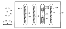
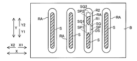
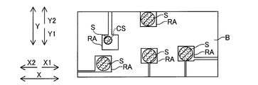
たとえば、図5に示すように、塗布装置1bの基板撮像部7が、一方側(X2側)から3番目の半田Sを塗布する所定箇所RAを撮像した場合、制御部8により半田Sの平面視における形状CS(二次元形状CS)が認識される。そして、図6に示すように、塗布装置1bの制御部8は、基板B上のFIマークの位置を基準位置としたときにおける、一方側(X2側)から3番目の所定箇所RAに塗布される半田Sの基準形状DSを取得する。制御部8は、半田Sの基準形状DSと半田Sの形状CSとの比較に基づいて、所定箇所RAの半田Sの検査結果の良または不良を判断する。
塗布装置1bの制御部8は、検査結果が不良であった場合に、半田Sの基準形状DSに基づいて、第1不足部分R1の平面内(XY平面内)における位置(第1不足位置SP1)を取得する。また、塗布装置1bの制御部8は、半田Sの基準形状DSに基づいて、第2不足部分R2の平面内(XY平面内)における位置(第2不足位置SP2)を取得する。なお、第1不足位置SP1および第2不足位置SP2は、各々特許請求の範囲の「不足位置」の一例である。
塗布装置1bの制御部8は、半田Sの基準形状DSに対する第1不足部分R1の割合を取得する。これにより、塗布装置1bの制御部8は、半田Sの基準形状DSを形成するために必要な半田Sの量と、半田Sの基準形状DSに対する第1不足部分R1の割合とに基づいて、第1不足部分R1に塗布する半田Sの量(第1不足量SQ1)を取得する。なお、第1不足量SQ1は、特許請求の範囲の「不足量」の一例である。
また、塗布装置1bの制御部8は、半田Sの基準形状DSに対する第2不足部分R2の割合を取得する。これにより、塗布装置1bの制御部8は、半田Sの基準形状DSを形成するために必要な半田Sの量と、半田Sの基準形状DSに対する第2不足部分R2の割合とに基づいて、第2不足部分R2に塗布する半田Sの量(第2不足量SQ2)を取得する。なお、第2不足量SQ2は、特許請求の範囲の「不足量」の一例である。
塗布装置1bの制御部8は、図7に示すように、第1不足位置SP1および第1不足量SQ1に基づいて、ディスペンスヘッド41により第1不足部分R1に半田Sを塗布させる。さらに、塗布装置1bの制御部8は、第2不足位置SP2および第2不足量SQ2に基づいて、ディスペンスヘッド41により第2不足部分R2に半田Sを塗布させる。このようにして、塗布装置1bでは、半田Sを塗布する所定箇所RAにおける補修箇所を補修している。ここで、所定箇所RAにおける補修箇所の補修は、ディスペンスヘッド41から半田Sを平面視において略円形状となるように塗布(点打ち)することにより行なっている。
〈基板作業処理のフローチャート〉
図8を参照して、基板作業プログラムBPにより実施される基板作業処理フローを説明する。
図8を参照して、基板作業プログラムBPにより実施される基板作業処理フローを説明する。
まず、ステップS1において、制御部8は、印刷装置1aにより印刷された基板B上の所定箇所RAの半田Sを検査する。すなわち、制御部8は、基板撮像部7の撮像により基板B上の半田Sを認識し、基板B上の半田Sの撮像結果と基準形状DSとを比較することにより、基板B上の半田Sを検査する。ステップS2において、制御部8は、基板B上の半田Sの検査結果が良か否かを判断する。制御部8は、基板B上の半田Sの検査が不良であった場合にステップS3に進む。制御部8は、基板B上の半田Sの検査が良であった場合に基板作業処理を終了する。
ステップS3において、制御部8は、ディスペンスヘッド41により塗布する半田Sの不足位置SPおよび不足量SQを設定する。ステップS4において、制御部8は、ディスペンスヘッド41により、不足位置SPに不足量SQ分の半田Sを塗布させ、ステップS1に戻る。これにより、半田Sの検査が良であると判断されるまで、補修が行なわれる。
(第1実施形態の効果)
第1実施形態では、以下のような効果を得ることができる。
第1実施形態では、以下のような効果を得ることができる。
第1実施形態では、上記のように、塗布装置1bは、基板B上の所定箇所RAに印刷された半田Sの量が不足している場合に、ディスペンスヘッド41により半田Sを塗布して補修する制御を行う制御部8を備えている。これにより、オペレータの手動による不良に対する作業を待つことなく自動で補修が行われるので、生産を停止することなく生産を継続することができる。この結果、補修が必要な基板Bが生じた場合にも、生産効率が大きく低下することを抑制することができる。
また、第1実施形態では、上記のように、制御部8は、基板B上の所定箇所RAに印刷された半田Sの検査により取得される半田Sの不足量SQに基づいて、ディスペンスヘッド41により半田Sを塗布して補修する制御を行うように構成されている。これにより、半田Sの不足量SQに基づく量を基板B上の所定箇所RAに塗布して補修することができるので、基板B上の所定箇所RAに適切な量の半田Sを塗布して補修することができる。
また、第1実施形態では、上記のように、制御部8は、基板B上の所定箇所RAに印刷された半田Sの検査により、半田Sの不足位置SPおよび不足位置SPにおける半田Sの不足量SQを取得するように構成されている。また、制御部8は、不足位置SPおよび不足量SQに基づいて、ディスペンスヘッド41により所定箇所RAにおける不足位置SPを補修する制御を行うように構成されている。これにより、半田Sの不足量SQに基づく量を基板B上の所定箇所RAにおける半田Sの不足位置SPに塗布して補修することができるので、基板B上の所定箇所RAの適切な位置に適切な量の半田Sを塗布することができる。この結果、より適切に補修を行なうことができる。
また、第1実施形態では、上記のように、塗布装置1bは、ディスペンスヘッド41に加えて、基板B上の所定箇所RAに印刷された半田Sを検査する基板撮像部7をさらに備えている。制御部8は、基板撮像部7により半田Sの検査を行うとともに、ディスペンスヘッド41により半田Sを塗布して補修する制御を行うように構成されている。これにより、同じ塗布装置1b内において所定箇所RAに塗布された半田Sの検査および基板B上の所定箇所RAの半田Sの補修を行うことができるので、所定箇所RAのディスペンスヘッド41による補修を迅速に行うことができる。
また、第1実施形態では、上記のように、ディスペンスヘッド41により半田Sを塗布して補修する制御を行う制御部8を含む塗布装置1bを備えている。これにより、所定箇所RAへの半田Sの塗布量が不足した基板Bを部品実装装置1cに供給することを抑制することができるので、部品実装システム1内において基板Bに対する作業が停止してしまうことを抑制することが可能である。この結果、補修が必要な基板Bが生じた場合に、生産効率が大きく低下することを抑制することが可能である。
(第2実施形態)
次に、図4および図9~図14を参照して、本発明の第2実施形態による部品実装システム201の構成について説明する。第2実施形態では、上記第1実施形態とは異なり、塗布装置201bが、第1実施形態の印刷装置1aの機能も有するように構成された例について説明する。なお、第2実施形態において、第1実施形態と同様の構成に関しては、同じ符号を付して説明を省略する。
次に、図4および図9~図14を参照して、本発明の第2実施形態による部品実装システム201の構成について説明する。第2実施形態では、上記第1実施形態とは異なり、塗布装置201bが、第1実施形態の印刷装置1aの機能も有するように構成された例について説明する。なお、第2実施形態において、第1実施形態と同様の構成に関しては、同じ符号を付して説明を省略する。
部品実装システム201では、上流から、塗布装置201bおよび部品実装装置1cの順に配置されている。塗布装置201bは、所定箇所RAへの半田Sの塗布を行なうとともに、所定箇所RAにおいて半田Sの塗布量過少および塗布抜けが発生したと判断した場合に、塗布装置201bにより所定箇所RAを補修する制御を行なうように構成されている。つまり、塗布装置201bは、第1実施形態の塗布装置1bの機能に加えて、第1実施形態の印刷装置1aの機能も兼ねている。部品実装装置1cは、塗布装置201bから搬出された基板Bに電子部品を実装するように構成されている。
〈基板作業処理〉
図10~図13に基づいて、塗布装置201bの制御部208により実施される基板作業プログラムBPについて説明する。
図10~図13に基づいて、塗布装置201bの制御部208により実施される基板作業プログラムBPについて説明する。
たとえば、図10に示すように、塗布装置201bの基板撮像部7が、一方側(X2側)から2番目の半田Sを塗布する所定箇所RAを撮像した場合、制御部208により半田Sの平面視における形状CS(二次元形状CS)が認識される。そして、図11に示すように、塗布装置201bの制御部208は、基板B上のFIマークの位置を基準位置としたときにおける、一方側(X2側)から2番目の所定箇所RAに塗布される半田Sの基準形状DSを取得する。制御部208は、半田Sの基準形状DSと半田Sの形状CSとの比較に基づいて、所定箇所RAの半田Sの検査結果の良または不良を判断する。
塗布装置201bの制御部208は、半田Sの基準形状DSに基づいて、第3不足部分R3の平面内(XY平面内)における位置(第3不足位置SP3)を取得する。塗布装置201bの制御部208は、半田Sの基準形状DSに対する第3不足部分R3の割合を取得する。これにより、塗布装置201bの制御部208は、半田Sの基準形状DSを形成するために必要な半田Sの量と、半田Sの基準形状DSに対する第3不足部分R3の割合とに基づいて、第3不足部分R3に塗布する半田Sの量(第3不足量SQ3)を取得する。なお、第3不足位置SP3および第3不足量SQ3は、それぞれ特許請求の範囲の「不足位置」および「不足量」の一例である。
塗布装置201bの制御部208は、基板B上の所定箇所RAに塗布された半田Sの第3不足量SQ3に応じて、ノズル241aの先端部と基板BとのクリアランスCRを調節する制御を行うように構成されている。具体的には、図12(A)に示すように、第3不足量SQ3が大きい場合には、ディスペンスヘッド41から塗布される半田Sの量が大きくなるので、制御部208は、ノズル241aの先端部と基板BとのクリアランスCRを大きくする。また、図12(B)に示すように、第3不足量SQ3が小さい場合には、ディスペンスヘッド41から塗布される半田Sの量が小さくなるので、制御部208は、ノズル241aの先端部と基板BとのクリアランスCRを小さくする。
また、制御部208は、ノズル241aの先端部と基板BとのクリアランスCRを小さくする場合において、ノズル241aの先端部と基板Bとが非接触の状態を保持させている。そして、制御部208は、ノズル241aの先端部と基板Bとが非接触の状態を保持するとともに、第3不足部分R3に半田Sを塗布するように構成されている。これにより、ノズル241aから正確な量の半田Sを第3不足部分R3に切り離すことが可能である。
塗布装置201bの制御部208は、図13に示すように、第3不足位置SP3および第3不足量SQ3に基づいて、ディスペンスヘッド41により第3不足部分R3に半田Sを塗布させる。このようにして、塗布装置201bでは、半田Sを塗布する所定箇所RAにおける補修箇所を補修している。なお、第2実施形態のその他の構成は、第1実施形態の構成と同様である。
〈基板作業処理のフローチャート〉
図14を参照して、基板作業プログラムBPにより実施される基板作業処理フローを説明する。
図14を参照して、基板作業プログラムBPにより実施される基板作業処理フローを説明する。
ステップS11において、制御部208は、ディスペンスヘッド41により基板B上の所定箇所RAに半田Sを塗布させる。そして、制御部208は、ステップS12~ステップS15のそれぞれにおいて、第1実施形態の検査処理のステップS1~ステップS4のそれぞれに対応する処理を行う。
(第2実施形態の効果)
第2実施形態では、以下のような効果を得ることができる。
第2実施形態では、以下のような効果を得ることができる。
第2実施形態では、上記のように、ディスペンスヘッド41は、半田Sが吐出されるノズル241aを含んでいる。制御部208は、基板B上の所定箇所RAに塗布された半田Sの第3不足量SQ3に応じて、ノズル241aの先端部と基板BとのクリアランスCRを調節する制御を行うように構成されている。これにより、ノズル241aの先端部と基板BとのクリアランスCRによりノズル241aの先端部と基板Bとが非接触となるので、ノズル241aの先端部の接触による基板B上の所定箇所に塗布された半田Sの形状の変形を抑制することができる。
また、第2実施形態では、上記のように、半田Sの不足量に応じてノズル241aの先端部と基板BとのクリアランスCRが調整されるので、基板B上の所定箇所RAの補修をより一層適切に行なうことができる。
(変形例)
なお、今回開示された実施形態は、全ての点で例示であって制限的なものではないと考えられるべきである。本発明の範囲は、上記した実施形態の説明ではなく請求の範囲によって示され、さらに請求の範囲と均等の意味および範囲内での全ての変更(変形例)が含まれる。
なお、今回開示された実施形態は、全ての点で例示であって制限的なものではないと考えられるべきである。本発明の範囲は、上記した実施形態の説明ではなく請求の範囲によって示され、さらに請求の範囲と均等の意味および範囲内での全ての変更(変形例)が含まれる。
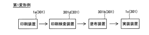
たとえば、上記第1および第2実施形態では、ヘッドユニット4に取り付けられた基板撮像部7により、基板B上の所定箇所RAの半田Sの撮像に基づく検査が行われている例を示したが、本発明はこれに限られない。本発明では、図4、図15および図16に示す第1変形例のように、基板上の所定箇所の半田の検査は、印刷装置1aの下流に配置された印刷検査装置301dにより行われてもよい。この場合、塗布装置301bの制御部308は、所定箇所に印刷された基板上の半田の印刷検査装置301dによる検査結果に基づいて、ディスペンスヘッドによる補修を行うように構成されている。また、制御部308による基板作業処理フローは図16に示すようになる。まず、ステップS21において、制御部308は、印刷検査装置301dの検査結果に基づいて、半田の不足位置および不足量を取得する。ステップS22において、制御部308は、ディスペンスヘッドにより塗布する半田の不足位置および不足量を設定する。ステップS23において、制御部308は、ディスペンスヘッドにより、不足位置に不足量分の半田を塗布させて、基板作業処理を終了する。
また、上記第1および第2実施形態では、基板撮像部7による基板B上の所定箇所RAの半田Sの撮像結果に基づいて、基板B上の所定箇所RAの半田Sの検査が行われる例を示したが、本発明はこれに限られない。本発明では、塗布装置1bは、半田Sの体積を測定可能な体積測定部を備えていてもよい。この場合、制御部8は、体積測定部により測定された半田Sの体積に基づいて、半田Sの不足量SQを取得するように構成されている。これにより、所定箇所RAに塗布または印刷された半田Sの量を正確に取得することができるので、不足量SQを正確に取得して基板B上の所定箇所RAにより適切な量の半田Sを塗布することができる。また、第1変形例に示す印刷検査装置301dが、体積測定部を備えていてもよい。なお、体積測定部は、半田Sの三次元形状を撮像可能なカメラ、または、半田Sの三次元形状を測定可能なレーザー計測部などを有する。
また、上記第1、第2実施形態および第1変形例では、基板B上の所定箇所RAにおける半田Sの補修が行われている例を示したが、本発明はこれに限られない。本発明では、基板上の所定箇所におけるフラックスなどの接着剤の補修が行われてもよい。
また、上記第1、第2実施形態および第1変形例では、制御部8(208、308)は、半田Sの不足位置SPに対して半田Sを不足量SQの分だけ塗布するように構成されている例を示したが、本発明はこれに限られない。本発明では、制御部は、不足量の半田を所定箇所の全体に塗布するように構成されていてもよい。
また、上記第1、第2実施形態および第1変形例では、制御部8(208、308)は、半田Sを不足量SQの分だけ塗布するように構成されている例を示したが、本発明はこれに限られない。本発明では、制御部は、一定量の半田を所定箇所に塗布するように構成されていてもよい。
また、上記第1~第2実施形態および第1変形例では、説明の便宜上、制御部8(208、308)の制御処理を、処理フローに沿って順番に処理を行うフロー駆動型のフローチャートを用いて説明した例について示したが、本発明はこれに限られない。本発明では、制御部の制御処理を、イベント単位で処理を実行するイベント駆動型(イベントドリブン型)の処理により行ってもよい。この場合、完全なイベント駆動型で行ってもよいし、イベント駆動およびフロー駆動を組み合わせて行ってもよい。
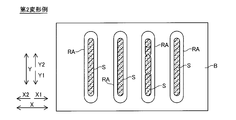
また、上記第1実施形態では、所定箇所RAにおける補修箇所の補修は、図7に示すように、ディスペンスヘッド41から半田Sを平面視において略円形状となるように塗布(点打ち)することにより行なっている例を示したが、本発明はこれに限られない。本発明では、所定箇所における補修箇所の補修は、図17に示す第2変形例のように、補修箇所の形状によっては、ディスペンスヘッドから半田を平面視において略矩形形状となるように塗布(線引き)することにより行なってもよい。
1、201、301 部品実装システム
1b、201b、301b 塗布装置(補修機能付き塗布装置)
1c 部品実装装置
7 基板撮像部(検査部)
8、208、308 制御部
41 ディスペンスヘッド(塗布部)
41a、241a ノズル
B 基板
CR クリアランス
RA 所定箇所
S 半田(液材)
SP 不足位置
SQ 不足量
1b、201b、301b 塗布装置(補修機能付き塗布装置)
1c 部品実装装置
7 基板撮像部(検査部)
8、208、308 制御部
41 ディスペンスヘッド(塗布部)
41a、241a ノズル
B 基板
CR クリアランス
RA 所定箇所
S 半田(液材)
SP 不足位置
SQ 不足量
Claims (7)
- 液材を基板に塗布する塗布部と、
前記基板上の所定箇所に塗布または印刷された前記液材の量が不足している場合に、前記塗布部により前記液材を塗布して補修する制御を行う制御部とを備える、補修機能付き塗布装置。 - 前記制御部は、前記基板上の前記所定箇所に塗布または印刷された前記液材の検査により取得される前記液材の不足量に基づいて、前記塗布部により前記液材を塗布して補修する制御を行うように構成されている、請求項1に記載の補修機能付き塗布装置。
- 前記制御部は、前記基板上の前記所定箇所に塗布または印刷された前記液材の検査により取得される前記液材の不足位置および前記不足位置における前記液材の不足量に基づいて、前記塗布部により前記所定箇所における前記不足位置を補修する制御を行うように構成されている、請求項2に記載の補修機能付き塗布装置。
- 前記塗布部に加えて、前記基板上の前記所定箇所に塗布または印刷された前記液材を検査する検査部をさらに備え、
前記制御部は、前記検査部により前記液材の検査を行うとともに、前記塗布部により前記液材を塗布して補修する制御を行うように構成されている、請求項1~3のいずれか1項に記載の補修機能付き塗布装置。 - 前記塗布部は、前記液材が吐出されるノズルを含み、
前記制御部は、前記基板上の前記所定箇所に塗布または印刷された前記液材の不足量に応じて、前記ノズルの先端部と前記基板とのクリアランスを調節する制御を行うように構成されている、請求項1~4のいずれか1項に記載の補修機能付き塗布装置。 - 前記検査部は、前記液材の体積を測定可能な体積測定部を含み、
前記制御部は、前記体積測定部により測定された前記液材の体積に基づいて、前記液材の不足量を取得するように構成されている、請求項4に記載の補修機能付き塗布装置。 - 液材を基板に塗布する塗布部と、前記基板上の所定箇所に塗布または印刷された前記液材の量が不足している場合に、前記塗布部により前記液材を塗布して補修する制御を行う制御部とを含む補修機能付き塗布装置と、
前記補修機能付き塗布装置の下流に配置され、前記補修機能付き塗布装置から搬出された前記基板に部品を実装する部品実装装置とを備える、部品実装システム。
Priority Applications (2)
| Application Number | Priority Date | Filing Date | Title |
|---|---|---|---|
| PCT/JP2017/034735 WO2019064341A1 (ja) | 2017-09-26 | 2017-09-26 | 補修機能付き塗布装置および部品実装システム |
| JP2019545419A JP7098642B2 (ja) | 2017-09-26 | 2017-09-26 | 補修機能付き塗布装置および部品実装システム |
Applications Claiming Priority (1)
| Application Number | Priority Date | Filing Date | Title |
|---|---|---|---|
| PCT/JP2017/034735 WO2019064341A1 (ja) | 2017-09-26 | 2017-09-26 | 補修機能付き塗布装置および部品実装システム |
Publications (1)
| Publication Number | Publication Date |
|---|---|
| WO2019064341A1 true WO2019064341A1 (ja) | 2019-04-04 |
Family
ID=65902879
Family Applications (1)
| Application Number | Title | Priority Date | Filing Date |
|---|---|---|---|
| PCT/JP2017/034735 Ceased WO2019064341A1 (ja) | 2017-09-26 | 2017-09-26 | 補修機能付き塗布装置および部品実装システム |
Country Status (2)
| Country | Link |
|---|---|
| JP (1) | JP7098642B2 (ja) |
| WO (1) | WO2019064341A1 (ja) |
Cited By (1)
| Publication number | Priority date | Publication date | Assignee | Title |
|---|---|---|---|---|
| CN116871116A (zh) * | 2023-07-11 | 2023-10-13 | 东莞勖祥精密模具有限公司 | 一种涂布头用涂布方法及涂布装置 |
Citations (5)
| Publication number | Priority date | Publication date | Assignee | Title |
|---|---|---|---|---|
| JP2000244107A (ja) * | 1999-02-24 | 2000-09-08 | Nec Corp | 吐出量制御機能付きディスペンサ及びクリーム半田の塗布方法 |
| JP2002166211A (ja) * | 2000-12-04 | 2002-06-11 | Sony Corp | ノズル高さ設定方法および塗布装置 |
| JP2005347387A (ja) * | 2004-06-01 | 2005-12-15 | Matsushita Electric Ind Co Ltd | 部品実装済み基板製造方法及び製造装置、並びに接合材料の供給状態異常修正方法 |
| JP2006108200A (ja) * | 2004-10-01 | 2006-04-20 | Hitachi Industries Co Ltd | はんだ印刷システム |
| JP2007222762A (ja) * | 2006-02-22 | 2007-09-06 | Shibaura Mechatronics Corp | ペースト塗布装置 |
Family Cites Families (1)
| Publication number | Priority date | Publication date | Assignee | Title |
|---|---|---|---|---|
| JP2015109397A (ja) * | 2013-12-06 | 2015-06-11 | パナソニックIpマネジメント株式会社 | 電子部品実装方法及び電子部品実装システム |
-
2017
- 2017-09-26 WO PCT/JP2017/034735 patent/WO2019064341A1/ja not_active Ceased
- 2017-09-26 JP JP2019545419A patent/JP7098642B2/ja active Active
Patent Citations (5)
| Publication number | Priority date | Publication date | Assignee | Title |
|---|---|---|---|---|
| JP2000244107A (ja) * | 1999-02-24 | 2000-09-08 | Nec Corp | 吐出量制御機能付きディスペンサ及びクリーム半田の塗布方法 |
| JP2002166211A (ja) * | 2000-12-04 | 2002-06-11 | Sony Corp | ノズル高さ設定方法および塗布装置 |
| JP2005347387A (ja) * | 2004-06-01 | 2005-12-15 | Matsushita Electric Ind Co Ltd | 部品実装済み基板製造方法及び製造装置、並びに接合材料の供給状態異常修正方法 |
| JP2006108200A (ja) * | 2004-10-01 | 2006-04-20 | Hitachi Industries Co Ltd | はんだ印刷システム |
| JP2007222762A (ja) * | 2006-02-22 | 2007-09-06 | Shibaura Mechatronics Corp | ペースト塗布装置 |
Cited By (1)
| Publication number | Priority date | Publication date | Assignee | Title |
|---|---|---|---|---|
| CN116871116A (zh) * | 2023-07-11 | 2023-10-13 | 东莞勖祥精密模具有限公司 | 一种涂布头用涂布方法及涂布装置 |
Also Published As
| Publication number | Publication date |
|---|---|
| JPWO2019064341A1 (ja) | 2020-08-13 |
| JP7098642B2 (ja) | 2022-07-11 |
Similar Documents
| Publication | Publication Date | Title |
|---|---|---|
| JP6346364B2 (ja) | ディスペンサーの供給ユニットを自動的に調整する方法 | |
| CN102037800B (zh) | 用于将材料分配到基板上的方法和装置 | |
| WO2014076968A1 (ja) | 電子部品装着システム | |
| TW201344824A (zh) | 電糊塗布裝置及電糊塗布方法以及晶粒接合器 | |
| JP2019047067A (ja) | 基板作業装置 | |
| WO2018207339A1 (ja) | 転写状態検査システム及び部品実装機 | |
| CN107079587A (zh) | 用于施加焊膏焊剂的方法和装置 | |
| TWI815930B (zh) | 從同步分配過渡到異步分配的系統及方法 | |
| JP2008198730A (ja) | 表面実装機、スクリーン印刷装置及び実装ライン | |
| TW201519718A (zh) | 焊膏印刷裝置及焊膏印刷方法 | |
| JP7098642B2 (ja) | 補修機能付き塗布装置および部品実装システム | |
| JP2017092342A (ja) | 導電性ボールを搭載するシステム | |
| GB2351347A (en) | Inspecting printing state of pattern eg on a printed circuit board | |
| JP4896855B2 (ja) | 部品実装システム | |
| JP2011018816A (ja) | 電子部品の装着方法 | |
| WO2017064777A1 (ja) | 部品実装装置 | |
| JP2009016499A5 (ja) | ||
| JP2009016499A (ja) | ペースト塗着装置 | |
| JP4459852B2 (ja) | 基板認識方法および部品実装システム | |
| WO2019049278A1 (ja) | スクリーン印刷機 | |
| JP2009152461A (ja) | 実装基板製造方法 | |
| KR20120081000A (ko) | 표면 형상 측정 장치 및 이를 이용한 스크린 프린터 관리 시스템 | |
| WO2021234848A1 (ja) | 部品実装システム | |
| JP7250157B2 (ja) | チェック装置 | |
| JPH0437090A (ja) | 接着剤塗布方法および電子部品固定用接着剤塗布装置 |
Legal Events
| Date | Code | Title | Description |
|---|---|---|---|
| 121 | Ep: the epo has been informed by wipo that ep was designated in this application |
Ref document number: 17926754 Country of ref document: EP Kind code of ref document: A1 |
|
| ENP | Entry into the national phase |
Ref document number: 2019545419 Country of ref document: JP Kind code of ref document: A |
|
| NENP | Non-entry into the national phase |
Ref country code: DE |
|
| 122 | Ep: pct application non-entry in european phase |
Ref document number: 17926754 Country of ref document: EP Kind code of ref document: A1 |