WO2019054239A1 - Module de conversion photoélectrique et procédé de fabrication de module de conversion photoélectrique - Google Patents
Module de conversion photoélectrique et procédé de fabrication de module de conversion photoélectrique Download PDFInfo
- Publication number
- WO2019054239A1 WO2019054239A1 PCT/JP2018/032774 JP2018032774W WO2019054239A1 WO 2019054239 A1 WO2019054239 A1 WO 2019054239A1 JP 2018032774 W JP2018032774 W JP 2018032774W WO 2019054239 A1 WO2019054239 A1 WO 2019054239A1
- Authority
- WO
- WIPO (PCT)
- Prior art keywords
- photoelectric conversion
- electrode layer
- region
- grid
- conversion module
- Prior art date
Links
- 238000006243 chemical reaction Methods 0.000 title claims abstract description 169
- 238000004519 manufacturing process Methods 0.000 title claims description 16
- 238000000034 method Methods 0.000 title description 12
- 238000002834 transmittance Methods 0.000 claims abstract description 30
- 239000000758 substrate Substances 0.000 claims description 17
- 230000015572 biosynthetic process Effects 0.000 claims description 15
- 238000009826 distribution Methods 0.000 claims description 5
- 239000010408 film Substances 0.000 description 24
- 239000000463 material Substances 0.000 description 24
- 239000004065 semiconductor Substances 0.000 description 15
- 230000004048 modification Effects 0.000 description 10
- 238000012986 modification Methods 0.000 description 10
- 230000008569 process Effects 0.000 description 8
- 238000013459 approach Methods 0.000 description 7
- 239000000047 product Substances 0.000 description 7
- 238000010586 diagram Methods 0.000 description 5
- 238000010304 firing Methods 0.000 description 4
- 239000011521 glass Substances 0.000 description 4
- 229910052751 metal Inorganic materials 0.000 description 4
- 239000002184 metal Substances 0.000 description 4
- 230000009467 reduction Effects 0.000 description 4
- XLOMVQKBTHCTTD-UHFFFAOYSA-N Zinc monoxide Chemical compound [Zn]=O XLOMVQKBTHCTTD-UHFFFAOYSA-N 0.000 description 3
- 239000013078 crystal Substances 0.000 description 3
- 238000005520 cutting process Methods 0.000 description 3
- 239000003574 free electron Substances 0.000 description 3
- 238000005259 measurement Methods 0.000 description 3
- 239000010409 thin film Substances 0.000 description 3
- 239000011701 zinc Substances 0.000 description 3
- 239000011248 coating agent Substances 0.000 description 2
- 238000000576 coating method Methods 0.000 description 2
- 239000004020 conductor Substances 0.000 description 2
- 229910052802 copper Inorganic materials 0.000 description 2
- 239000010949 copper Substances 0.000 description 2
- 230000007423 decrease Effects 0.000 description 2
- 239000002270 dispersing agent Substances 0.000 description 2
- 229910021476 group 6 element Inorganic materials 0.000 description 2
- 238000007641 inkjet printing Methods 0.000 description 2
- 239000003960 organic solvent Substances 0.000 description 2
- 239000002245 particle Substances 0.000 description 2
- 229910052709 silver Inorganic materials 0.000 description 2
- VYZAMTAEIAYCRO-UHFFFAOYSA-N Chromium Chemical compound [Cr] VYZAMTAEIAYCRO-UHFFFAOYSA-N 0.000 description 1
- RYGMFSIKBFXOCR-UHFFFAOYSA-N Copper Chemical compound [Cu] RYGMFSIKBFXOCR-UHFFFAOYSA-N 0.000 description 1
- 230000005355 Hall effect Effects 0.000 description 1
- ZOKXTWBITQBERF-UHFFFAOYSA-N Molybdenum Chemical compound [Mo] ZOKXTWBITQBERF-UHFFFAOYSA-N 0.000 description 1
- RTAQQCXQSZGOHL-UHFFFAOYSA-N Titanium Chemical compound [Ti] RTAQQCXQSZGOHL-UHFFFAOYSA-N 0.000 description 1
- 229910003363 ZnMgO Inorganic materials 0.000 description 1
- 229910052782 aluminium Inorganic materials 0.000 description 1
- 239000011230 binding agent Substances 0.000 description 1
- 239000000919 ceramic Substances 0.000 description 1
- 229910052804 chromium Inorganic materials 0.000 description 1
- 239000011651 chromium Substances 0.000 description 1
- 150000001875 compounds Chemical class 0.000 description 1
- 230000007797 corrosion Effects 0.000 description 1
- 238000005260 corrosion Methods 0.000 description 1
- 230000006378 damage Effects 0.000 description 1
- 230000006866 deterioration Effects 0.000 description 1
- 230000005611 electricity Effects 0.000 description 1
- 229910052733 gallium Inorganic materials 0.000 description 1
- 229910052737 gold Inorganic materials 0.000 description 1
- 229910052738 indium Inorganic materials 0.000 description 1
- AMGQUBHHOARCQH-UHFFFAOYSA-N indium;oxotin Chemical compound [In].[Sn]=O AMGQUBHHOARCQH-UHFFFAOYSA-N 0.000 description 1
- 229910052750 molybdenum Inorganic materials 0.000 description 1
- 239000011733 molybdenum Substances 0.000 description 1
- 239000012299 nitrogen atmosphere Substances 0.000 description 1
- 238000007645 offset printing Methods 0.000 description 1
- 230000003287 optical effect Effects 0.000 description 1
- 229910052760 oxygen Inorganic materials 0.000 description 1
- 230000035699 permeability Effects 0.000 description 1
- 238000007639 printing Methods 0.000 description 1
- 239000011347 resin Substances 0.000 description 1
- 229920005989 resin Polymers 0.000 description 1
- 238000007650 screen-printing Methods 0.000 description 1
- 239000003566 sealing material Substances 0.000 description 1
- 229910052711 selenium Inorganic materials 0.000 description 1
- 239000011265 semifinished product Substances 0.000 description 1
- 239000004332 silver Substances 0.000 description 1
- 238000004544 sputter deposition Methods 0.000 description 1
- 229910052717 sulfur Inorganic materials 0.000 description 1
- 229910052719 titanium Inorganic materials 0.000 description 1
- 239000010936 titanium Substances 0.000 description 1
- 238000007740 vapor deposition Methods 0.000 description 1
- 239000011787 zinc oxide Substances 0.000 description 1
Images


Classifications
-
- H—ELECTRICITY
- H01—ELECTRIC ELEMENTS
- H01L—SEMICONDUCTOR DEVICES NOT COVERED BY CLASS H10
- H01L31/00—Semiconductor devices sensitive to infrared radiation, light, electromagnetic radiation of shorter wavelength or corpuscular radiation and specially adapted either for the conversion of the energy of such radiation into electrical energy or for the control of electrical energy by such radiation; Processes or apparatus specially adapted for the manufacture or treatment thereof or of parts thereof; Details thereof
- H01L31/04—Semiconductor devices sensitive to infrared radiation, light, electromagnetic radiation of shorter wavelength or corpuscular radiation and specially adapted either for the conversion of the energy of such radiation into electrical energy or for the control of electrical energy by such radiation; Processes or apparatus specially adapted for the manufacture or treatment thereof or of parts thereof; Details thereof adapted as photovoltaic [PV] conversion devices
- H01L31/042—PV modules or arrays of single PV cells
- H01L31/0445—PV modules or arrays of single PV cells including thin film solar cells, e.g. single thin film a-Si, CIS or CdTe solar cells
- H01L31/046—PV modules composed of a plurality of thin film solar cells deposited on the same substrate
- H01L31/0465—PV modules composed of a plurality of thin film solar cells deposited on the same substrate comprising particular structures for the electrical interconnection of adjacent PV cells in the module
-
- H—ELECTRICITY
- H01—ELECTRIC ELEMENTS
- H01L—SEMICONDUCTOR DEVICES NOT COVERED BY CLASS H10
- H01L31/00—Semiconductor devices sensitive to infrared radiation, light, electromagnetic radiation of shorter wavelength or corpuscular radiation and specially adapted either for the conversion of the energy of such radiation into electrical energy or for the control of electrical energy by such radiation; Processes or apparatus specially adapted for the manufacture or treatment thereof or of parts thereof; Details thereof
- H01L31/02—Details
- H01L31/0224—Electrodes
- H01L31/022408—Electrodes for devices characterised by at least one potential jump barrier or surface barrier
- H01L31/022425—Electrodes for devices characterised by at least one potential jump barrier or surface barrier for solar cells
- H01L31/022433—Particular geometry of the grid contacts
-
- H—ELECTRICITY
- H01—ELECTRIC ELEMENTS
- H01L—SEMICONDUCTOR DEVICES NOT COVERED BY CLASS H10
- H01L31/00—Semiconductor devices sensitive to infrared radiation, light, electromagnetic radiation of shorter wavelength or corpuscular radiation and specially adapted either for the conversion of the energy of such radiation into electrical energy or for the control of electrical energy by such radiation; Processes or apparatus specially adapted for the manufacture or treatment thereof or of parts thereof; Details thereof
- H01L31/02—Details
- H01L31/0224—Electrodes
- H01L31/022466—Electrodes made of transparent conductive layers, e.g. TCO, ITO layers
-
- H—ELECTRICITY
- H01—ELECTRIC ELEMENTS
- H01L—SEMICONDUCTOR DEVICES NOT COVERED BY CLASS H10
- H01L31/00—Semiconductor devices sensitive to infrared radiation, light, electromagnetic radiation of shorter wavelength or corpuscular radiation and specially adapted either for the conversion of the energy of such radiation into electrical energy or for the control of electrical energy by such radiation; Processes or apparatus specially adapted for the manufacture or treatment thereof or of parts thereof; Details thereof
- H01L31/18—Processes or apparatus specially adapted for the manufacture or treatment of these devices or of parts thereof
- H01L31/1884—Manufacture of transparent electrodes, e.g. TCO, ITO
Definitions
- the present invention relates to a photoelectric conversion module having a grid electrode and a method of manufacturing the photoelectric conversion module.
- a photoelectric conversion module such as a solar cell module including a plurality of photoelectric conversion cells is known (Patent Document 1 below).
- the photoelectric conversion cell includes a transparent electrode layer located on the light receiving surface, a back electrode layer located on the surface opposite to the light receiving surface, and a transparent electrode And a photoelectric conversion layer between the layer and the back electrode layer.
- the electrical resistance value of the transparent electrode layer is generally higher than the electrical resistance value of the opaque electrode layer made of metal. Therefore, when the current generated by photoelectric conversion flows through the transparent electrode layer, a loss of power occurs due to the electric resistance value of the transparent electrode layer.
- a grid electrode (collecting electrode) made of a thin metal line may be provided on the transparent electrode layer.
- the current flowing through the transparent electrode layer is collected by the grid electrode, whereby the current path flowing through the transparent electrode layer is shortened. Therefore, the loss of power due to the electric resistance value of the transparent electrode layer can be reduced.
- the grid electrode is generally non-transparent, it blocks light incident on the photoelectric conversion layer. Therefore, the short circuit current (Isc) generated in the photoelectric conversion cell is reduced due to the reduction of the light reaching the photoelectric conversion layer.
- a photoelectric conversion module includes a strip-shaped photoelectric conversion cell including a first electrode layer, a second electrode layer, and a photoelectric conversion layer between the first electrode layer and the second electrode layer. And a plurality of grid electrodes provided side by side in the first direction in the photoelectric conversion cell and extending in a direction intersecting the first direction, and at least one of the first electrode layer and the second electrode layer is transparent.
- An electrode layer wherein the transparent electrode layer includes a first region and a second region, and the second region has a sheet resistance smaller than the sheet resistance in the first region, and a film thickness in the first region
- the film thickness or the transmittance smaller than the transmittance in the first region, and the distance between the grid electrodes adjacent to each other in the first direction in the first region is the first direction in the second region Next to each other Serial smaller than the spacing of the grid electrodes each other.
- a first electrode layer, a second electrode layer, and a photoelectric conversion layer between the first electrode layer and the second electrode layer are provided on a substrate. And forming a strip-shaped photoelectric conversion cell, wherein at least one of the first electrode layer and the second electrode layer is a transparent electrode layer, and the sheet resistance of the transparent electrode layer, the film And measuring the thickness or transmittance, and forming a plurality of grid electrodes which are provided in the first direction in the photoelectric conversion cell and extend in the direction intersecting the first direction.
- the grid electrode is formed such that the distance between the grid electrodes is smaller as the area having a larger sheet resistance, the area having a smaller film thickness, or the area having a larger transmittance.
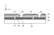
- FIG. 3 is a schematic cross-sectional view of the photoelectric conversion module taken along line 3A-3A of FIG. 2; It is a schematic perspective view of the photoelectric conversion module in area
- FIG. 5 is a schematic cross-sectional view of the photoelectric conversion module taken along line 5A-5A of FIG. It is a typical top view of the photoelectric conversion module in field 6R of FIG. It is a typical top view of the photoelectric conversion module in field 7R of FIG.
- connection part of the 1st grid electrode concerning the 1st modification, and the 2nd grid electrode. It is a typical top view of the connection part of the 1st grid electrode concerning the 2nd modification, and the 2nd grid electrode. It is a typical top view of the connection part of the 1st grid electrode concerning the 3rd modification, and the 2nd grid electrode. It is a typical sectional view showing the cell formation process in the manufacturing method of a photoelectric conversion module. It is a schematic diagram which shows the 1st grid formation process of forming a 1st grid electrode. It is a schematic diagram which shows the 2nd grid formation process of forming a 2nd grid electrode. It is a schematic diagram which shows 1 step of the process of forming wiring. It is a schematic diagram which shows the step following FIG. It is a schematic diagram which shows the process of cutting off a part of photoelectric conversion module.
- FIG. 1 is a schematic top view of the photoelectric conversion module according to the first embodiment.
- FIG. 2 is a schematic top view of the photoelectric conversion module in the region 2R of FIG.
- FIG. 3 is a schematic cross-sectional view of the photoelectric conversion module taken along line 3A-3A of FIG.
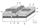
- FIG. 4 is a schematic perspective view of the photoelectric conversion module in the region 4R of FIG.
- FIG. 5 is a schematic cross-sectional view of the photoelectric conversion module taken along line 5A-5A of FIG.
- FIG. 6 is a schematic top view of the photoelectric conversion module in the region 6R of FIG.
- FIG. 7 is a schematic top view of the photoelectric conversion module in the region 7R of FIG.
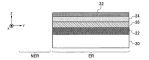
- the photoelectric conversion module 10 may be an integrated-type thin film photoelectric conversion module including a plurality of photoelectric conversion cells 12 integrated on a substrate 20.
- the photoelectric conversion module 10 is a solar cell module that converts light energy into electrical energy.
- the substrate 20 may be made of, for example, glass, ceramics, resin, metal or the like.
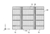
- the photoelectric conversion cells 12 may have a substantially band-like shape as viewed in the direction orthogonal to the main surface of the substrate 20. Each photoelectric conversion cell 12 may extend in the first direction (Y direction in the drawing). The plurality of photoelectric conversion cells 12 are arranged in a second direction (X direction in the drawing) intersecting the first direction. The photoelectric conversion cells 12 adjacent to each other may be separated from one another by the division parts P1, P2, and P3 extending in the first direction.
- Each photoelectric conversion cell 12 may include at least a first electrode layer 22, a second electrode layer 24, and a photoelectric conversion layer 26.
- the photoelectric conversion layer 26 is provided between the first electrode layer 22 and the second electrode layer 24.
- the first electrode layer 22 is provided between the photoelectric conversion layer 26 and the substrate 20.
- the second electrode layer 24 is located on the opposite side to the substrate 20 with respect to the photoelectric conversion layer 26.
- the second electrode layer 24 may be configured of a transparent electrode layer.
- the second electrode layer 24 is formed of a transparent electrode layer, light incident on the photoelectric conversion layer 26 or emitted from the photoelectric conversion layer 26 passes through the second electrode layer 24.
- the first electrode layer 22 may be formed of an opaque electrode layer or may be formed of a transparent electrode layer.
- the first electrode layer 22 is preferably formed of, for example, a metal such as molybdenum, titanium, or chromium from the viewpoint of corrosion resistance to a group VI element.
- the second electrode layer 24 is formed of an n-type semiconductor, more specifically, a material having n-type conductivity, a wide band gap, and a relatively low resistance. Ru.
- the second electrode layer 24 may be made of, for example, zinc oxide (ZnO) to which a group III element is added, or indium tin oxide (ITO). In this case, the second electrode layer 24 can have the functions of the n-type semiconductor and the transparent electrode layer.
- the photoelectric conversion layer 26 may include, for example, a p-type semiconductor.
- the photoelectric conversion layer 26 includes a group I element (Cu, Ag, Au, etc.), a group III element (Al, Ga, In, etc.) and a group VI element (O, S, Se, It is formed by the compound semiconductor containing Te etc.).
- the photoelectric conversion layer 26 is not limited to those described above, and may be made of any material that causes photoelectric conversion.
- the configuration of the photoelectric conversion cell 12 is not limited to the above embodiment, but can take various embodiments.
- the photoelectric conversion cell 12 may have a configuration in which both an n-type semiconductor and a p-type semiconductor are sandwiched between the first electrode layer and the second electrode layer.
- the second electrode layer may not be composed of an n-type semiconductor.
- the photoelectric conversion cell 12 is not limited to the pn junction type structure, but includes the pn junction type structure including an intrinsic semiconductor layer (i type semiconductor) between the n type semiconductor and the p type semiconductor. You may have.
- the photoelectric conversion cell 12 may have a buffer layer (not shown) between the photoelectric conversion layer 26 and the second electrode layer 24.
- the buffer layer may be a semiconductor material having the same conductivity type as the second electrode layer 24 or may be a semiconductor material having a different conductivity type.
- the buffer layer may be made of a material having a higher electrical resistance than the second electrode layer 24.
- the buffer layer may be a Zn-based buffer layer, a Cd-based buffer layer, or an In-based buffer layer.
- the Zn-based buffer layer may be, for example, ZnS, ZnO, Zn (OH) or ZnMgO, or a mixed crystal or laminate of these.
- the Cd-based buffer layer may be, for example, CdS, CdO or Cd (OH), or a mixed crystal or laminate of these.
- the In-based buffer layer may be, for example, InS, InO or In (OH), or a mixed crystal or laminate of these.
- the first electrode layers 22 of the photoelectric conversion cells 12 adjacent to each other are electrically separated from each other by the division portion P1.
- the second electrode layers 24 of the photoelectric conversion cells 12 adjacent to each other are electrically separated from each other by the dividing portion P3.
- the photoelectric conversion layers 26 of the photoelectric conversion cells 12 adjacent to each other are separated from each other by the division parts P2 and P3.
- the photoelectric conversion module 10 may have an electrical connection 34 between the photoelectric conversion cells 12 adjacent to each other.
- the electrical connection portion 34 electrically connects the photoelectric conversion cells 12 adjacent to each other in series.
- the electrical connection portion 34 is formed by a portion that is continuous with the second electrode layer 24.
- the electrical connection portion 34 may be made of the same material as the second electrode layer 24.
- the electrical connection 34 may be made of a conductive material different from that of the second electrode layer 24.
- the electrical connection portion 34 may be made of the same material as the material of the first grid electrode 31 or the second grid electrode 32 described later.
- the electrical connection portion 34 extends in the thickness direction of the photoelectric conversion module 10 at the second divided portion P 2, whereby the first electrode layer 22 of one photoelectric conversion cell 12 and the second electrode layer 24 of the other photoelectric conversion cell 12. And are electrically connected to each other.
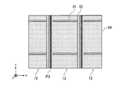
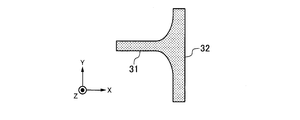
- the photoelectric conversion module 10 has a plurality of first grid electrodes 31 provided side by side in a first direction (Y direction in the drawing) in each photoelectric conversion cell 12. Each first grid electrode 31 extends in a second direction (X direction in the figure) intersecting the first direction.
- the first grid electrode 31 may be provided on the second electrode layer 24 of each photoelectric conversion cell 12.
- the first grid electrode 31 may be made of a material having higher conductivity than the transparent electrode layer constituting the second electrode layer 24.
- the first grid electrode 31 may be in direct contact with the transparent electrode layer.
- the width of the first grid electrode 31 in the first direction (Y direction in the drawing) may be, for example, 5 to 100 ⁇ m.
- the thickness of the first grid electrode 31 may be, for example, 0.1 to 20 ⁇ m.
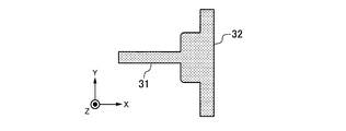
- a second grid electrode 32 extending in the first direction may be provided at an end of the first grid electrode 31 in the second direction (X direction in the drawing).
- the second grid electrode 32 is connected to the first grid electrode 31 at one end of the first grid electrode 31.
- the width of the second grid electrode 32 in the second direction (X direction in the figure) may be, for example, 5 to 200 ⁇ m.
- the thickness of the second grid electrode 32 may be, for example, 0.1 to 20 ⁇ m.
- the thickness is larger than the thickness of the first grid electrode 31 and the second grid electrode 32 (or the electrical connection portion 34) at a position distant from the intersection point.
- the thickness of the first grid electrode 31 may be gradually increased toward the intersection of the first grid electrode 31 and the second grid electrode 32 (or the electrical connection portion 34).
- the thickness of the second grid electrode 32 (or the electrical connection portion 34) may be gradually increased toward the intersection of the first grid electrode 31 and the second grid electrode 32 (or the electrical connection portion 34).
- the photoelectric conversion module 10 has a wiring 50 for supplying power to the photoelectric conversion module 10 or taking it out of the photoelectric conversion module 10.
- the wiring 50 may be provided adjacent to the photoelectric conversion cell 12 located at the end of the photoelectric conversion module 10 in the second direction (the X direction in the drawing).
- the transparent electrode layer constituting the second electrode layer 24 may include a region 2R as shown in FIG. 2 and a region 6R as shown in FIG.
- the area 2R and the area 6R are disposed in the same photoelectric conversion cell 12.
- the distance between the first grid electrodes 31 adjacent to each other in the first direction (Y direction) in the region 2R is smaller than the distance between the first grid electrodes 31 adjacent to each other in the first direction (Y direction) in the region 6R.
- the region 6R of the second electrode layer 24 has a sheet resistance smaller than the sheet resistance in the region 2R, a film thickness larger than the film thickness in the region 2R, or a transmittance smaller than the transmittance in the region 2R.
- the distance between the first grid electrodes 31 described above is the distance between the center line of an arbitrary first grid electrode 31 and the center line of the first grid electrode 31 adjacent thereto.
- the second electrode layer 24 may further include a region 7R as shown in FIG.
- the region 6R and the region 7R are disposed in different photoelectric conversion cells 12.
- the distance between the first grid electrodes 31 adjacent to each other in the first direction (Y direction) in the region 7R is smaller than the distance between the first grid electrodes 31 adjacent to each other in the first direction (Y direction) in the region 6R.
- the region 6R of the second electrode layer 24 has a sheet resistance smaller than the sheet resistance in the region 7R, a film thickness larger than the film thickness in the region 7R, or a transmittance smaller than the transmittance in the region 7R.
- the second electrode layer 24 of the photoelectric conversion module 10 has a distribution in sheet resistance, film thickness or transmittance, and a distance between the first grid electrodes 31 adjacent to each other in the first direction (Y direction). Is smaller as the sheet resistance is larger, smaller as the film thickness is smaller, or smaller as the transmittance is larger.
- the distribution of the electrical resistance value in which both the transparent electrode layer and the first grid electrode 31 are combined approaches uniform. In this manner, the overall sheet resistance is made uniform, and the density of the first grid electrode 31 (area density of grid electrodes per unit area in the plan view of the photoelectric conversion module) in unnecessary areas is lowered. It is possible to balance the problem of the loss of power due to the electric resistance value of the transparent electrode layer and the problem of the reduction of the short circuit current due to the shielding of light by the first grid electrode.
- the sheet resistance of the transparent electrode layer increases as the film thickness of the transparent electrode layer decreases. Furthermore, the sheet resistance of the transparent electrode layer is considered to be higher as the transmittance of the transparent electrode layer is larger. It is considered that this is because when the transmittance of the transparent electrode layer is large, the film thickness of the transparent electrode layer is generally small or the carrier concentration of the transparent electrode layer is low.
- both the transparent electrode layer and the first grid electrode 31 are combined. It is considered that the distribution of electrical resistance values approaches uniform. Even in this case, the problem of power loss due to the electric resistance value of the transparent electrode layer can be achieved by making the overall sheet resistance close to uniform and lowering the density of the first grid electrode 31 in unnecessary areas. And the problem of reducing the short circuit current due to the shielding of light by the first grid electrode can be balanced.
- the film thickness or transmittance of the transparent electrode layer can be measured more easily than the sheet resistance of the transparent electrode layer in the production line. Therefore, when setting the space
- FIG. 8 is a schematic top view of the connection portion of the first grid electrode 31 and the second grid electrode 32 according to the first modification.
- the width of the first grid electrode 31 in the first direction (Y direction) is wider as the second grid electrode 32 is approached.
- the width of the first grid electrode 31 in the first direction (Y direction) gradually increases as the second grid electrode 32 is approached.
- the width of the second grid electrode 32 in the second direction (X direction) may be gradually expanded as it approaches the first grid electrode 31.
- FIG. 9 is a schematic top view of the connection portion of the first grid electrode 31 and the second grid electrode 32 according to the second modification.
- the width of the first grid electrode 31 in the first direction (Y direction) is wider as the second grid electrode 32 is approached.
- the width of the first grid electrode 31 in the first direction (Y direction) gradually increases as it approaches the second grid electrode 32.
- the width of the second grid electrode 32 in the second direction (X direction) may be gradually expanded stepwise as it approaches the first grid electrode 31.
- the electricity in the connection portion between the first grid electrode 31 and the second grid electrode 32 is obtained. Connection failure or increase in electrical resistance can be suppressed.
- FIG. 10 is a schematic top view of the connection portion of the first grid electrode 31 and the second grid electrode 32 according to the third modification.
- the first grid electrode 31 approaches the second grid electrode 32 and is bent in the first direction (Y direction).
- Y direction the first direction
- the first grid electrode 31 may increase in thickness as it approaches the second grid electrode 32.
- each layer can be appropriately formed by a film forming means such as a sputtering method or a vapor deposition method.
- a strip-shaped photoelectric conversion cell 12 including a first electrode layer 22, a second electrode layer 24, and a photoelectric conversion layer 26 between the first electrode layer 22 and the second electrode layer 24 on a substrate 20.
- Cell formation step Specifically, first, the material forming the first electrode layer 22 is formed on the substrate 20. The material forming the first electrode layer 22 is formed in the region across the plurality of photoelectric conversion cells 12. The materials of the substrate 20 and the first electrode layer 22 are as described above. Next, a part of the material forming the first electrode layer 22 is removed in the form of a thin line to form a first divided portion P1 for forming the first electrode layer 22 into a plurality of strip shapes. The removal of part of the material making up the first electrode layer 22 can be performed by means such as a laser or a needle.
- a material forming the photoelectric conversion layer 26 is formed on the first electrode layer 22.
- the material of the photoelectric conversion layer 26 is as described above. Under the present circumstances, the material which comprises the photoelectric converting layer 26 may be filled also in the 1st division part P1. Instead of this, the first divided portion P1 may be filled with another insulating member different from the material of the photoelectric conversion layer 26.
- a part of the material forming the photoelectric conversion layer 26 is removed in a thin line shape, thereby forming a second divided portion P2 for forming the photoelectric conversion layer 26 into a plurality of strip shapes.
- a material forming the second electrode layer 24 is formed on the photoelectric conversion layer 26.
- the material of the second electrode layer 24 is as described above.
- the second electrode layer 24 is preferably a transparent electrode layer.
- the material that constitutes the second electrode layer 24 may also be filled in the second divided portion P2.
- the second electrode layer 24 filled also in the second divided portion P2 constitutes the above-described electrical connection portion 34.
- the second divided portion P2 may be filled with another conductive material different from the material of the second electrode layer 24.
- the second electrode layer 24 and the photoelectric conversion layer 26 are formed into a plurality of strip shapes by removing a part of the material constituting the second electrode layer 24 and the photoelectric conversion layer 26 in a thin line shape.
- the divided portion P3 is formed.
- the method of manufacturing the photoelectric conversion module may have a step of measuring the sheet resistance, the film thickness or the transmittance of the transparent electrode layer constituting the second electrode layer 24.
- the sheet resistance of the transparent electrode layer can be measured by, for example, a resistance measurement device by a four-terminal method or a resistance measurement device using a Hall effect.
- the film thickness of the transparent electrode layer can be measured by, for example, a spectrophotometer, an optical interference film thickness meter, an SEM (scanning electron microscope), a step difference meter or a laser microscope.
- the transmittance of the transparent electrode layer can be measured, for example, by a spectrophotometer.
- the measurement of the sheet resistance, film thickness or transmittance of the transparent electrode layer may be performed on a photoelectric conversion module used as a finished product, and a dummy photoelectric conversion module or dummy not used as a finished product May be performed on the glass substrate of When the photoelectric conversion module 10 is mass-produced, the sheet resistance, film thickness, or transmittance distribution of the transparent electrode layer in the same production line (lot) is substantially the same among products.
- a product not to be used as a finished product for example, a semi-finished product formed to the photoelectric conversion layer 26 on the substrate 20 or a dummy glass substrate on which the transparent electrode layer is formed is taken out and taken out
- the sheet resistance, film thickness or transmittance of the transparent electrode layer may be measured on the glass substrate of Thereby, the sheet resistance, film thickness, or transmittance of the transparent electrode layer of the photoelectric conversion module 10 used as a product in the same production line (lot) can be estimated.
- the method of manufacturing the photoelectric conversion module may have a grid forming step of forming grid electrodes 31 and 32 after the cell forming step.
- the grid formation step may include a first grid formation step and a second grid formation step.
- the first grid formation process may be performed at any timing before or after the second grid formation process.
- the grid formation process may be performed before the third divided portion P3 is formed.
- first grid forming step a plurality of first grid electrodes are provided in the photoelectric conversion cell 12 side by side in a first direction (Y direction in the drawing) and extend in a second direction (X direction in the drawing) intersecting the first direction.
- second grid electrode 32 extending in the first direction (the Y direction in the drawing) as described above is formed.
- the first grid electrode 31 and / or the second grid electrode 32 can be formed by, for example, ink jet printing, screen printing, gravure offset printing, or flexo printing.
- ink jet printing screen printing, gravure offset printing, or flexo printing.
- coating of a conductive ink for example, inkjet printing is demonstrated using FIG.12 and FIG.13.
- the conductive ink 102 may be composed of conductive particles such as silver and copper, an organic solvent, and a conductive paste containing a dispersant. In addition, the conductive ink 102 may contain a binder as needed.
- the conductive ink 102 is formed on the second electrode layer 24 by being ejected from the nozzle 100. The conductive ink 102 is preferably fired after being applied. The baking of the conductive ink 102 vaporizes the organic solvent and the dispersant, and the conductive particles remain in a predetermined coating pattern. Thereby, the first grid electrode 31 and the second grid electrode 32 are formed.
- the firing temperature of the conductive ink 102 may be in the range of 100 ° C. to 200 ° C.
- the firing temperature of the conductive ink 102 is preferably 150 ° C. or less in order to suppress the deterioration or destruction of the photoelectric conversion cell that constitutes the CIS-based photoelectric conversion module.
- the firing of the conductive ink 102 is more preferably performed in the air (more preferably, dry air) or in a nitrogen atmosphere.
- the firing time may be, for example, in the range of 5 to 60 minutes.
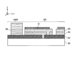
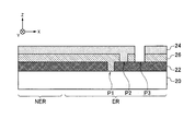
- the start point S1 at which the application of the conductive ink 102 is started in one photoelectric conversion module is located in the ineffective area NER not contributing to the electromotive force of the photoelectric conversion module (see FIG. 12).
- the conductive ink 102 is discharged from the nozzle 100 while scanning the nozzle 100 of the inkjet head from the start point S1 in the second direction (X direction), thereby the second direction Conductive ink 102 is formed.
- the start point S2 at which the application of the conductive ink 102 is started in one photoelectric conversion module is preferably located in the non-effective area NER not contributing to the electromotive force of the photoelectric conversion module.
- the conductive ink 102 is discharged from the nozzle 100 while scanning the nozzle 100 of the ink jet head in the first direction (Y direction) from the start point S2 to the second direction. Conductive ink 102 is formed.
- the non-effective area NER described above is defined by an area which does not contribute to photoelectric conversion in the middle of manufacturing or after completion of the product.
- the non-effective area NER is separated, for example, by cutting off the first electrode layer 22, the photoelectric conversion layer 26 and the second electrode layer 24 from the photoelectric conversion cell 12 contributing to photoelectric conversion, at least the area where the second electrode layer 24 is cut off. It may be an area which does not contribute to the photoelectric conversion, or an area cut away from the photoelectric conversion module 10 in production.
- a period (lead time) in which the conductive ink 102 is not applied may exist before the application of the ink to the start points S1 and S2 is started. If the conductive ink 102 is dried during this period, the conductive ink 102 may not be accurately applied to the start points S1 and S2. In this aspect, since the start points S1 and S2 are located in the ineffective area NER, even if the conductive ink 102 is not accurately applied to the start points S1 and S2, the performance of the photoelectric conversion module is unlikely to be affected.
- the method of manufacturing a photoelectric conversion module includes the step of removing at least a portion of the second electrode layer 24, preferably the second electrode layer 24 and the photoelectric conversion layer 26.
- the region from which at least the second electrode layer 24 is removed constitutes a non-effective region NER.
- the start point S1 at which the application of the conductive ink 102 is started may be located in the non-effective area NER.
- the above-described wiring 50 may be formed in a region where at least the second electrode layer 24 is removed.
- the area where at least the second electrode layer 24 is removed may be an end area of the photoelectric conversion module 10 in the second direction (X direction).
- the method of manufacturing the photoelectric conversion module may further include the step of cutting out a region including the start point S2 where application of the conductive ink 102 is started.
- the photoelectric conversion module 10 described in the first embodiment is obtained as described above.
- at least the second electrode layer 24 in the portion corresponding to the non-effective area NER is removed.
- the present invention is not limited to this, and the wiring 50 may be formed on the second electrode layer 24 without removing the second electrode layer 24.
- a division groove may be formed between the wiring 50 and the photoelectric conversion cell 12 adjacent to the wiring 50 to divide the non-effective region NER and the effective region ER contributing to photoelectric conversion.
- the division grooves can be formed, for example, by removing the first electrode layer 22, the photoelectric conversion layer 26, and the second electrode layer 24.
- the photoelectric conversion module 10 may be sealed by a transparent sealing material (not shown).
- the first grid electrode 31 and the second grid electrode 32 are provided on the second electrode layer 24.
- the first grid electrode 31 and the second grid electrode 32 may be provided between the photoelectric conversion layer 26 and the second electrode layer 24.
- the second electrode layer 24 is configured of a transparent electrode layer.
- the first electrode layer 22 may be constituted by a transparent electrode layer.
- the second electrode layer 24 may be constituted by a transparent electrode layer or may be constituted by an opaque electrode layer.
- the first grid electrode 31 and the second grid electrode 32 be provided adjacent to the first electrode layer 22.
- the substrate 20 may be made of a transparent substrate.
- all the first grid electrodes 31 have the same length in the second direction (X direction).
- the lengths of the first grid electrodes 31 in the second direction (X direction) may be different from each other in the same photoelectric conversion cell 12 or between different photoelectric conversion cells 12.
- the first grid electrode long in the second direction (X direction) and the first grid electrode short in the second direction (X direction) may be arranged in a predetermined pattern in the first direction (Y direction).
- the thin film photoelectric conversion module (having the dividing portions P1 to P3) having the integrated structure has been described as an example, but the present invention is not limited thereto.
- the present invention is also applicable to a photoelectric conversion module having no part P1 to P3.
- the intervals for forming the grid electrodes may be determined according to the sheet resistance, film thickness, and transmittance of the transparent electrode layer included in the photoelectric conversion module. .
- photoelectric conversion module 12 photoelectric conversion cell 20 substrate 22 first electrode layer 24 second electrode layer (n-type semiconductor) 26 Photoelectric conversion layer (p-type semiconductor) 31 first grid electrode 32 second grid electrode 50 wiring
Landscapes
- Engineering & Computer Science (AREA)
- Microelectronics & Electronic Packaging (AREA)
- Physics & Mathematics (AREA)
- Condensed Matter Physics & Semiconductors (AREA)
- Electromagnetism (AREA)
- General Physics & Mathematics (AREA)
- Computer Hardware Design (AREA)
- Power Engineering (AREA)
- Sustainable Development (AREA)
- Life Sciences & Earth Sciences (AREA)
- Sustainable Energy (AREA)
- Manufacturing & Machinery (AREA)
- Photovoltaic Devices (AREA)
Abstract
L'invention concerne un module de conversion photoélectrique (10) comprenant : une cellule de conversion photoélectrique en forme de bande (12) comprenant une première couche d'électrode (22), une seconde couche d'électrode (24), et une couche de conversion photoélectrique (26) ; et une pluralité d'électrodes de grille (31). La première couche d'électrode et/ou la seconde couche d'électrode est une couche d'électrode transparente. La couche d'électrode transparente comprend une première et une seconde région. La seconde région a une résistance en feuille qui est inférieure à la résistance en feuille dans la première région, une épaisseur de film qui est plus grande que l'épaisseur de film dans la première région, ou une transmittance qui est inférieure à la transmittance dans la première région. Le jeu entre les électrodes de grille adjacentes l'une à l'autre dans la première direction dans la première région est plus petit que le jeu entre les électrodes de grille adjacentes l'une à l'autre dans la première direction dans la seconde région.
Priority Applications (3)
| Application Number | Priority Date | Filing Date | Title |
|---|---|---|---|
| CN201880059780.3A CN111247643B (zh) | 2017-09-15 | 2018-09-04 | 光电变换模块以及制造光电变换模块的方法 |
| JP2019542010A JP7127042B2 (ja) | 2017-09-15 | 2018-09-04 | 光電変換モジュール及び光電変換モジュールを製造する方法 |
| US16/647,160 US20210028322A1 (en) | 2017-09-15 | 2018-09-04 | Photoelectric conversion module and method for manufacturing photoelectric conversion module |
Applications Claiming Priority (2)
| Application Number | Priority Date | Filing Date | Title |
|---|---|---|---|
| JP2017-178367 | 2017-09-15 | ||
| JP2017178367 | 2017-09-15 |
Publications (1)
| Publication Number | Publication Date |
|---|---|
| WO2019054239A1 true WO2019054239A1 (fr) | 2019-03-21 |
Family
ID=65722794
Family Applications (1)
| Application Number | Title | Priority Date | Filing Date |
|---|---|---|---|
| PCT/JP2018/032774 WO2019054239A1 (fr) | 2017-09-15 | 2018-09-04 | Module de conversion photoélectrique et procédé de fabrication de module de conversion photoélectrique |
Country Status (4)
| Country | Link |
|---|---|
| US (1) | US20210028322A1 (fr) |
| JP (1) | JP7127042B2 (fr) |
| CN (1) | CN111247643B (fr) |
| WO (1) | WO2019054239A1 (fr) |
Families Citing this family (2)
| Publication number | Priority date | Publication date | Assignee | Title |
|---|---|---|---|---|
| DE102021127720A1 (de) * | 2021-10-25 | 2023-04-27 | Heliatek Gmbh | Elektrisch leitfähige Beschichtung eines elektrischen Bauelements zur elektrisch leitfähigen Kontaktierung einer außerhalb der Beschichtung angeordneten Sammelschiene |
| WO2023141884A1 (fr) * | 2022-01-27 | 2023-08-03 | Triumph Science & Technology Group Co., Ltd | Imprimante à jet d'encre pour former des lignes conductrices entrecroisées de module solaire à film mince et système de métallisation automatisé |
Citations (5)
| Publication number | Priority date | Publication date | Assignee | Title |
|---|---|---|---|---|
| JPH03234066A (ja) * | 1990-02-09 | 1991-10-18 | Sanyo Electric Co Ltd | 光起電力装置 |
| JP2000058888A (ja) * | 1998-08-03 | 2000-02-25 | Sanyo Electric Co Ltd | 太陽電池及びその製造方法 |
| JP2012124328A (ja) * | 2010-12-08 | 2012-06-28 | Ulvac Japan Ltd | 太陽電池 |
| WO2013094233A1 (fr) * | 2011-12-21 | 2013-06-27 | 三菱電機株式会社 | Cellule solaire, procédé de production de celle-ci et module à cellule solaire |
| US20160284882A1 (en) * | 2013-09-17 | 2016-09-29 | Lg Innotek Co., Ltd. | Solar Cell |
Family Cites Families (11)
| Publication number | Priority date | Publication date | Assignee | Title |
|---|---|---|---|---|
| US4590327A (en) * | 1984-09-24 | 1986-05-20 | Energy Conversion Devices, Inc. | Photovoltaic device and method |
| JPS63143878A (ja) * | 1986-12-08 | 1988-06-16 | Matsushita Electric Ind Co Ltd | シリコン太陽電池 |
| US5859397A (en) * | 1996-05-17 | 1999-01-12 | Canon Kabushiki Kaisha | Process for the production of a photovoltaic element |
| JP2008277233A (ja) * | 2007-04-03 | 2008-11-13 | Oike Ind Co Ltd | 透明導電性フィルム及びその製造方法 |
| EP2296186B1 (fr) * | 2008-05-22 | 2018-08-29 | Kaneka Corporation | Dispositif de conversion photoélectrique à film mince et procédé de fabrication associé |
| JP2011216189A (ja) * | 2010-03-31 | 2011-10-27 | Sony Corp | 光電変換装置及び光電変換装置モジュール |
| JP5829101B2 (ja) * | 2011-10-28 | 2015-12-09 | オリンパス株式会社 | 神経刺激装置および埋込型心臓治療装置 |
| JP2013219143A (ja) * | 2012-04-06 | 2013-10-24 | Sharp Corp | 薄膜太陽電池モジュールおよび薄膜太陽電池モジュールの製造方法 |
| JP2015195341A (ja) * | 2014-03-24 | 2015-11-05 | 三菱電機株式会社 | 光電変換素子および光電変換素子の製造方法 |
| JP6422426B2 (ja) * | 2014-12-09 | 2018-11-14 | 三菱電機株式会社 | 太陽電池 |
| KR101821394B1 (ko) * | 2016-01-14 | 2018-01-23 | 엘지전자 주식회사 | 태양전지 |
-
2018
- 2018-09-04 WO PCT/JP2018/032774 patent/WO2019054239A1/fr active Application Filing
- 2018-09-04 JP JP2019542010A patent/JP7127042B2/ja active Active
- 2018-09-04 US US16/647,160 patent/US20210028322A1/en not_active Abandoned
- 2018-09-04 CN CN201880059780.3A patent/CN111247643B/zh active Active
Patent Citations (5)
| Publication number | Priority date | Publication date | Assignee | Title |
|---|---|---|---|---|
| JPH03234066A (ja) * | 1990-02-09 | 1991-10-18 | Sanyo Electric Co Ltd | 光起電力装置 |
| JP2000058888A (ja) * | 1998-08-03 | 2000-02-25 | Sanyo Electric Co Ltd | 太陽電池及びその製造方法 |
| JP2012124328A (ja) * | 2010-12-08 | 2012-06-28 | Ulvac Japan Ltd | 太陽電池 |
| WO2013094233A1 (fr) * | 2011-12-21 | 2013-06-27 | 三菱電機株式会社 | Cellule solaire, procédé de production de celle-ci et module à cellule solaire |
| US20160284882A1 (en) * | 2013-09-17 | 2016-09-29 | Lg Innotek Co., Ltd. | Solar Cell |
Also Published As
| Publication number | Publication date |
|---|---|
| CN111247643B (zh) | 2023-09-22 |
| JPWO2019054239A1 (ja) | 2020-10-22 |
| JP7127042B2 (ja) | 2022-08-29 |
| US20210028322A1 (en) | 2021-01-28 |
| CN111247643A (zh) | 2020-06-05 |
Similar Documents
| Publication | Publication Date | Title |
|---|---|---|
| KR101210168B1 (ko) | 태양광 발전장치 및 이의 제조방법 | |
| EP2416376A2 (fr) | Appareil de production d'énergie photovoltaïque solaire et procédé de fabrication de celui-ci | |
| KR100999797B1 (ko) | 태양광 발전장치 및 이의 제조방법 | |
| KR101072089B1 (ko) | 태양전지 및 이의 제조방법 | |
| KR20110001305A (ko) | 태양전지 및 이의 제조방법 | |
| KR101262455B1 (ko) | 태양광 발전장치 및 이의 제조방법 | |
| KR101168810B1 (ko) | 태양광 발전장치 및 이의 제조방법 | |
| JP7127042B2 (ja) | 光電変換モジュール及び光電変換モジュールを製造する方法 | |
| KR101201542B1 (ko) | 박막태양전지 및 그 제조방법 | |
| KR20120012325A (ko) | 태양광 발전장치 및 이의 제조방법 | |
| KR101550927B1 (ko) | 태양전지 및 이의 제조방법 | |
| KR101114079B1 (ko) | 태양광 발전장치 및 이의 제조방법 | |
| CN111247642B (zh) | 光电变换模块以及制造光电变换模块的方法 | |
| JP7053202B2 (ja) | 光電変換モジュール | |
| KR101055019B1 (ko) | 태양광 발전장치 및 이의 제조방법 | |
| KR101241467B1 (ko) | 태양전지 및 이의 제조방법 | |
| US20140144479A1 (en) | Photoelectric conversion module | |
| KR101349429B1 (ko) | 태양광 발전장치 | |
| KR20120086447A (ko) | 태양전지 및 이의 제조방법 | |
| KR101172178B1 (ko) | 태양광 발전장치 및 이의 제조방법 | |
| JP2011023443A (ja) | 太陽電池、太陽電池の製造方法 | |
| JP2019054166A (ja) | 光電変換モジュールの製造方法 | |
| JP2013149699A (ja) | 集積化太陽電池の製造方法 | |
| KR101543034B1 (ko) | 팁 및 이를 이용한 태양전지의 제조방법 | |
| KR101091499B1 (ko) | 팁, 태양전지 및 팁을 이용한 태양전지의 제조방법 |
Legal Events
| Date | Code | Title | Description |
|---|---|---|---|
| 121 | Ep: the epo has been informed by wipo that ep was designated in this application |
Ref document number: 18857131 Country of ref document: EP Kind code of ref document: A1 |
|
| WWE | Wipo information: entry into national phase |
Ref document number: 2019542010 Country of ref document: JP |
|
| NENP | Non-entry into the national phase |
Ref country code: DE |
|
| 122 | Ep: pct application non-entry in european phase |
Ref document number: 18857131 Country of ref document: EP Kind code of ref document: A1 |