WO2019031211A1 - 電力変換装置 - Google Patents
電力変換装置 Download PDFInfo
- Publication number
- WO2019031211A1 WO2019031211A1 PCT/JP2018/027482 JP2018027482W WO2019031211A1 WO 2019031211 A1 WO2019031211 A1 WO 2019031211A1 JP 2018027482 W JP2018027482 W JP 2018027482W WO 2019031211 A1 WO2019031211 A1 WO 2019031211A1
- Authority
- WO
- WIPO (PCT)
- Prior art keywords
- terminal
- power
- coexistence
- semiconductor module
- bus bar
- Prior art date
- Legal status (The legal status is an assumption and is not a legal conclusion. Google has not performed a legal analysis and makes no representation as to the accuracy of the status listed.)
- Ceased
Links
Images


Classifications
-
- H—ELECTRICITY
- H02—GENERATION; CONVERSION OR DISTRIBUTION OF ELECTRIC POWER
- H02M—APPARATUS FOR CONVERSION BETWEEN AC AND AC, BETWEEN AC AND DC, OR BETWEEN DC AND DC, AND FOR USE WITH MAINS OR SIMILAR POWER SUPPLY SYSTEMS; CONVERSION OF DC OR AC INPUT POWER INTO SURGE OUTPUT POWER; CONTROL OR REGULATION THEREOF
- H02M7/00—Conversion of AC power input into DC power output; Conversion of DC power input into AC power output
- H02M7/003—Constructional details, e.g. physical layout, assembly, wiring or busbar connections
-
- H—ELECTRICITY
- H02—GENERATION; CONVERSION OR DISTRIBUTION OF ELECTRIC POWER
- H02M—APPARATUS FOR CONVERSION BETWEEN AC AND AC, BETWEEN AC AND DC, OR BETWEEN DC AND DC, AND FOR USE WITH MAINS OR SIMILAR POWER SUPPLY SYSTEMS; CONVERSION OF DC OR AC INPUT POWER INTO SURGE OUTPUT POWER; CONTROL OR REGULATION THEREOF
- H02M7/00—Conversion of AC power input into DC power output; Conversion of DC power input into AC power output
- H02M7/42—Conversion of DC power input into AC power output without possibility of reversal
- H02M7/44—Conversion of DC power input into AC power output without possibility of reversal by static converters
- H02M7/48—Conversion of DC power input into AC power output without possibility of reversal by static converters using discharge tubes with control electrode or semiconductor devices with control electrode
- H02M7/53—Conversion of DC power input into AC power output without possibility of reversal by static converters using discharge tubes with control electrode or semiconductor devices with control electrode using devices of a triode or transistor type requiring continuous application of a control signal
- H02M7/537—Conversion of DC power input into AC power output without possibility of reversal by static converters using discharge tubes with control electrode or semiconductor devices with control electrode using devices of a triode or transistor type requiring continuous application of a control signal using semiconductor devices only, e.g. single switched pulse inverters
- H02M7/5387—Conversion of DC power input into AC power output without possibility of reversal by static converters using discharge tubes with control electrode or semiconductor devices with control electrode using devices of a triode or transistor type requiring continuous application of a control signal using semiconductor devices only, e.g. single switched pulse inverters in a bridge configuration
- H02M7/53871—Conversion of DC power input into AC power output without possibility of reversal by static converters using discharge tubes with control electrode or semiconductor devices with control electrode using devices of a triode or transistor type requiring continuous application of a control signal using semiconductor devices only, e.g. single switched pulse inverters in a bridge configuration with automatic control of output voltage or current
-
- H—ELECTRICITY
- H10—SEMICONDUCTOR DEVICES; ELECTRIC SOLID-STATE DEVICES NOT OTHERWISE PROVIDED FOR
- H10W—GENERIC PACKAGES, INTERCONNECTIONS, CONNECTORS OR OTHER CONSTRUCTIONAL DETAILS OF DEVICES COVERED BY CLASS H10
- H10W40/00—Arrangements for thermal protection or thermal control
- H10W40/20—Arrangements for cooling
- H10W40/22—Arrangements for cooling characterised by their shape, e.g. having conical or cylindrical projections
-
- H—ELECTRICITY
- H10—SEMICONDUCTOR DEVICES; ELECTRIC SOLID-STATE DEVICES NOT OTHERWISE PROVIDED FOR
- H10W—GENERIC PACKAGES, INTERCONNECTIONS, CONNECTORS OR OTHER CONSTRUCTIONAL DETAILS OF DEVICES COVERED BY CLASS H10
- H10W40/00—Arrangements for thermal protection or thermal control
- H10W40/40—Arrangements for thermal protection or thermal control involving heat exchange by flowing fluids
- H10W40/47—Arrangements for thermal protection or thermal control involving heat exchange by flowing fluids by flowing liquids, e.g. forced water cooling
-
- H—ELECTRICITY
- H10—SEMICONDUCTOR DEVICES; ELECTRIC SOLID-STATE DEVICES NOT OTHERWISE PROVIDED FOR
- H10W—GENERIC PACKAGES, INTERCONNECTIONS, CONNECTORS OR OTHER CONSTRUCTIONAL DETAILS OF DEVICES COVERED BY CLASS H10
- H10W74/00—Encapsulations, e.g. protective coatings
- H10W74/10—Encapsulations, e.g. protective coatings characterised by their shape or disposition
-
- H—ELECTRICITY
- H10—SEMICONDUCTOR DEVICES; ELECTRIC SOLID-STATE DEVICES NOT OTHERWISE PROVIDED FOR
- H10W—GENERIC PACKAGES, INTERCONNECTIONS, CONNECTORS OR OTHER CONSTRUCTIONAL DETAILS OF DEVICES COVERED BY CLASS H10
- H10W90/00—Package configurations
-
- H—ELECTRICITY
- H02—GENERATION; CONVERSION OR DISTRIBUTION OF ELECTRIC POWER
- H02P—CONTROL OR REGULATION OF ELECTRIC MOTORS, ELECTRIC GENERATORS OR DYNAMO-ELECTRIC CONVERTERS; CONTROLLING TRANSFORMERS, REACTORS OR CHOKE COILS
- H02P27/00—Arrangements or methods for the control of AC motors characterised by the kind of supply voltage
- H02P27/04—Arrangements or methods for the control of AC motors characterised by the kind of supply voltage using variable-frequency supply voltage, e.g. inverter or converter supply voltage
- H02P27/06—Arrangements or methods for the control of AC motors characterised by the kind of supply voltage using variable-frequency supply voltage, e.g. inverter or converter supply voltage using DC to AC converters or inverters
Definitions
- Patent Document 1 discloses a power conversion device in which a semiconductor module containing an upper arm switching element and a semiconductor module containing a lower arm switching element are arranged adjacent to each other.
- the positive electrode terminal of the upper arm semiconductor module connected to the positive electrode bus bar and the negative electrode terminal of the lower arm semiconductor module connected to the negative electrode bus bar are arranged adjacent to each other.
- the positive electrode bus bar protrudes from a terminal connected to the positive electrode terminal.
- the negative electrode bus bar projects a terminal connected to the negative electrode terminal.
- One each of these terminals is separately arrange
- the present disclosure seeks to provide a power converter that is easy to reduce the inductance.
- One aspect of the present disclosure is a power conversion device including a switching circuit unit including a plurality of upper arm switching elements connected to a positive electrode wire and a plurality of lower arm switching elements connected to a negative electrode wire, With multiple bus bars, And a plurality of semiconductor modules formed by projecting power terminals from the module main body,
- the bus bar it has a positive electrode bus bar which constitutes the positive electrode wire and a negative electrode bus bar which constitutes the negative electrode wire
- the semiconductor module a first semiconductor module including the positive arm terminal which is the power terminal connected to the positive bus bar while incorporating the upper arm switching element, the lower arm switching element and the negative bus bar.
- a second semiconductor module provided with a negative electrode terminal which is the power terminal to be connected;
- the first semiconductor module and the second semiconductor module are disposed in a state in which the positive electrode terminal and the negative electrode terminal are opposed to each other in a direction orthogonal to the protruding direction,
- the positive electrode bus bar and the negative electrode bus bar both have coexistence arrangement parts disposed between the positive electrode terminal and the negative electrode terminal when viewed from the projecting direction of the power terminal, At least a part of the coexistence / arrangement portion is in the power conversion device disposed in the space between the positive electrode terminal and the negative electrode terminal.
- the positive electrode bus bar and the negative electrode bus bar each have the coexistence arrangement portion. And, at least a part of the coexistence arrangement portion is arranged to coexist in the space between the positive electrode terminal and the negative electrode terminal arranged to face each other. According to this configuration, the positive electrode bus bar and the negative electrode bus bar are closely arranged in the coexistence arrangement portion. As a result, the inductance in the bus bar can be reduced.
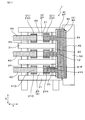
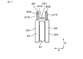
- FIG. 1 is a plan view of a power conversion device according to a first embodiment
- FIG. 2 is a circuit diagram of the power conversion device in the first embodiment
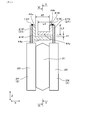
- FIG. 3 is a perspective view of a semiconductor module and a bus bar in Embodiment 1
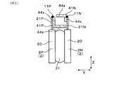
- FIG. 4 is a cross-sectional view of the semiconductor module and the coexistence and placement unit in the first embodiment
- 5 is a cross-sectional view taken along line VV of FIG. 6
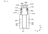
- FIG. 7 is a cross-sectional view of the semiconductor module and the output interposed portion in the first embodiment
- FIG. 8 is a plan view of the power conversion device in a state in which the bus bar is removed in the first embodiment
- FIG. 9 is a cross-sectional view of the semiconductor module and the coexistence / arrangement portion in the second embodiment
- FIG. 10 is a cross-sectional view of a semiconductor module and a coexistence arrangement portion in the third embodiment
- FIG. 11 is a cross-sectional view of the semiconductor module and the coexistence / disposition portion in the fourth embodiment
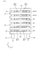
- FIG. 12 is a circuit diagram of the power conversion device in the fifth embodiment.
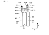
- the power conversion device 1 of the present embodiment is a switching circuit unit including a plurality of upper arm switching elements 20 u connected to the positive electrode wiring and a plurality of lower arm switching elements 20 d connected to the negative electrode wiring. It is equipped with 101.
- the power conversion device 1 has a plurality of bus bars 4 and a plurality of semiconductor modules 2 formed by projecting the power terminals 21 from the module body 20.
- the power conversion device 1 includes, as the bus bars 4, a positive electrode bus bar 4P that configures positive electrode wiring and a negative electrode bus bar 4N that configures negative electrode wiring.
- the power conversion device 1 includes a first semiconductor module 2P and a second semiconductor module 2N as the semiconductor module 2.
- the first semiconductor module 2P incorporates an upper arm switching element 20u.
- the first semiconductor module 2P also includes a positive terminal 21P, which is a power terminal 21 connected to the positive bus bar 4P.
- the second semiconductor module 2N incorporates the lower arm switching element 20d.
- the second semiconductor module 2N also includes a negative terminal 21N that is a power terminal 21 connected to the negative bus bar 4N.
- the first semiconductor module 2P and the second semiconductor module 2N are disposed in a state in which the positive electrode terminal 21P and the negative electrode terminal 21N are opposed in the direction orthogonal to the projecting direction.
- the positive electrode bus bar 4P and the negative electrode bus bar 4N each have coexistence placement portions 41P and 41N.
- the coexistence placement portions 41P and 41N are portions disposed between the positive electrode terminal 21P and the negative electrode terminal 21N when viewed from the projecting direction of the power terminal 21 as shown in FIG. At least a portion of the coexistence / arrangement portions 41P and 41N is disposed in the space between the positive electrode terminal 21P and the negative electrode terminal 21N.
- the coexistence / arrangement portions 41P and 41N are entirely disposed in the space between the positive electrode terminal 21P and the negative electrode terminal 21N.
- a direction parallel to the protruding direction of the power terminal 21 is referred to as the Z direction as appropriate.
- the direction in which the positive electrode terminal 21P and the negative electrode terminal 21N face each other is referred to as the X direction as appropriate.
- a direction orthogonal to both the X direction and the Z direction is referred to as a Y direction as appropriate.
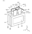
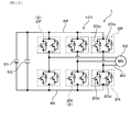
- the power conversion device 1 of the present embodiment is, for example, an inverter mounted on a vehicle. Then, as shown in FIG. 2, power conversion between DC power and AC power is performed between the DC power supply 51 and the three-phase AC rotating electrical machine 52.
- the switching circuit unit 101 of the power conversion device 1 includes three-phase legs. That is, the three-phase legs are connected in parallel with each other between the positive electrode wiring connected to the positive electrode of the DC power supply 51 and the negative electrode wiring connected to the negative electrode of the DC power supply 51.
- Each leg is formed of an upper arm switching element 20 u and a lower arm switching element 20 d connected in series with each other.
- connection point between the upper arm switching element 20 u and the lower arm switching element 20 d in each leg is connected to the three electrodes of the rotary electric machine 52 via the output wiring. Further, a capacitor 53 is connected between the DC power supply 51 and the switching circuit unit 101 so as to suspend the positive electrode wire and the negative electrode wire. In addition, flywheel diodes are connected in reverse parallel to the respective switching elements.
- the switching element can be formed of an IGBT.
- IGBT is an abbreviation for Insulated Gate Bipolar Transistor, that is, an insulated gate bipolar transistor.
- the switching element can also be a MOSFET.
- MOSFET is an abbreviation for Metal Oxide Semiconductor Field Effect Transistor, or metal oxide field effect transistor.
- the positive electrode wiring is configured by the positive electrode bus bar 4P.
- the negative electrode wiring is configured by the negative electrode bus bar 4N.
- the output wiring is configured by the output bus bar 4O.
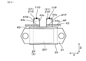
- Each semiconductor module 2 has two power terminals 21. As shown in FIG. 5, the first semiconductor module 2P has, as the power terminal 21, a positive electrode terminal 21P and an output terminal 21O. As shown in FIG. 6, the second semiconductor module 2N has, as a power terminal 21, a negative electrode terminal 21N and an output terminal 21O.
- the upper arm switching elements 20 u and the lower arm switching elements 20 d are respectively incorporated in the individual semiconductor modules 2.
- one upper arm switching element 20u is incorporated in one first semiconductor module 2P
- one lower arm switching element 20d is incorporated in one second semiconductor module 2N.
- the positive electrode terminal 21P is at the same potential as the collector of the upper arm switching element 20u
- the output terminal 21O is at the same potential as the emitter of the upper arm switching element 20u
- the output terminal 21O is at the same potential as the collector of the lower arm switching element 20d
- the negative terminal 21N is at the same potential as the emitter of the lower arm switching element 20d.
- Each semiconductor module 2 projects two power terminals 21 from the module body 20 in the same direction as the Z direction. Moreover, although illustration is abbreviate
- the module main body 20 exposes the heat sink 201 on both main surfaces thereof.
- the first semiconductor module 2P and the second semiconductor module 2N are disposed such that the heat dissipation plates 201 face each other.
- the plurality of semiconductor modules 2 are stacked in the X direction together with the plurality of cooling pipes 31 so that the first semiconductor modules 2P and the second semiconductor modules 2N are alternately arranged.
- the cooling pipe 31 is disposed so as to be in thermal contact with the heat dissipation plate 201 of the semiconductor module 2.
- the cooling pipe 31 is provided with a refrigerant flow path through which the refrigerant flows.
- the cooling pipes 31 adjacent to each other in the X direction are connected by the connecting pipe 32 in the vicinity of both ends in the Y direction. Further, the cooling pipe 31 disposed at one end in the X direction is provided with a refrigerant introduction pipe 33 for introducing the refrigerant and a refrigerant discharge pipe 34 for discharging the refrigerant.
- the cooling pipe 31 is made of a metal having excellent thermal conductivity, such as an aluminum alloy.
- the power terminal 21 of the semiconductor module 2 protrudes further than the cooling pipe 31 in the Z direction. The power terminals 21 of the plurality of semiconductor modules 2 project to the same side in the Z direction.
- a capacitor 53 is disposed on one side in the Y direction with respect to the stacked portion of the semiconductor module 2.
- the two power terminals 21 in each semiconductor module 2 are provided with the positive electrode terminal 21P or the negative electrode terminal 21N closer to the capacitor 53 than the output terminal 21O in the Y direction.
- An output bus bar 4O is connected to the output terminal 21O.
- Each output bus bar 4O is connected to both the output terminals 21O of the first semiconductor module 2P and the second semiconductor module 2N adjacent in the X direction.
- the output bus bar 4O is formed to extend in the lateral direction Y from the connection with the output terminal 21O.
- a positive bus bar 4P and a negative bus bar 4N are disposed so as to connect the positive electrode and the negative electrode of the capacitor 53 to the power terminal 21 of the semiconductor module 2.
- the positive electrode bus bar 4P and the negative electrode bus bar 4N are integrated with the capacitor 53.
- Positive electrode bus bar 4P and negative electrode bus bar 4N each have main body plate portion 42 disposed so as to overlap each other in the Z direction, and a plurality of branch portions 43 extending from main body plate portion 42 to power terminal 21 in the Y direction. . A part of this branch part 43 becomes the above-mentioned coexistence arrangement parts 41P and 41N.
- Each branch portion 43 is connected to one positive terminal 21P and one negative terminal 21N adjacent in the X direction. Then, counting from one end in the X direction, between the semiconductor modules 2 of the first and second stages, between the semiconductor modules 2 of the third and fourth stages, and the fifth and sixth stages
- the coexistence placement units 41P and 41N are disposed between the semiconductor modules 2 of FIG. That is, between the power terminals 21 adjacent to each other in the X direction, there are portions where the coexistence / arrangement portions 41P and 41N are disposed and portions where the coexistence / disposition portions 41P and 41N are not disposed.
- the coexistence / arrangement portions 41P and 41N have opposing portions arranged so that the main surfaces thereof face each other.
- the coexistence / arrangement portions 41P and 41N have, as opposing portions, an array opposing portion 44x that opposes the array direction of the positive electrode terminal 21P and the negative electrode terminal 21N, that is, the X direction.
- the coexistence / arrangement portions 41P and 41N have, as opposing portions, a projecting opposing portion 44z opposing in the projecting direction of the power terminal 21, that is, the Z direction. That is, in the present embodiment, the coexistence / arrangement parts 41P and 41N have both the line opposing part 44x and the protruding opposing part 44z as the opposing part.
- the coexistence placement units 41P and 41N are substantially L-shaped in a cross section orthogonal to the Y direction.
- the coexistence placement portions 41P and 41N are formed by bending one end edge in the X direction of the end portions of the branch portions 43 of the bus bars 4 in one of the Z directions.
- a portion standing in the Z direction is the line facing portion 44 x, and a protruding facing portion 44 z is formed in a portion of the branch portion 43 where the main surface is directed in the Z direction.
- the erecting direction of the row opposing portion 44x from the projecting opposing portion 44z is the same as the projecting direction of the power terminal 21.
- the distance d1 between the pair of coexistence portions 41P and 41N in the protrusion facing portion 44z is smaller than the distance d2 between the pair of coexistence portions 41P and 41N in the row facing portion 44x.
- the distance between the protrusion opposing portion 44z of the coexistence arrangement portion 41P in the positive electrode bus bar 4P and the protrusion opposing portion 44z of the coexistence arrangement portion 41N in the negative electrode bus bar 4N is a distance d1.
- the distance between the alignment facing portion 44x of the coexistence arranging portion 41P in the positive electrode bus bar 4P and the alignment opposing portion 44x of the coexistence arranging portion 41N in the negative electrode bus bar 4N is a distance d2.
- these intervals d1 and d2 have a relation of d2> d1.
- the length L1 of the protrusion facing portion 44z in the direction in which the positive electrode terminal 21P and the negative electrode terminal 21N are aligned, ie, the X direction, is longer than the length L2 of the row facing portion 44x in the protruding direction of the power terminal 21, ie, the Z direction. .
- the coexistence placement part in which the protruding facing part 44z is disposed closer to the module main body 20 has the protruding facing part 44z in the module body than the connection part with the power terminal 21. It is placed near 20.
- the protrusion opposing portion 44 z is disposed at a position closer to the module main body 20 in the coexistence arrangement portion 41 P of the positive electrode bus bar 4 P. Therefore, the protrusion opposing portion 44z of the coexistence arrangement portion 41P of the positive electrode bus bar 4P is disposed at a position closer to the module body 20 than the connection portion 11P.
- each of the bus bars 4 the row facing portion 44 x is superimposed on the power terminal 21 in the X direction.
- the end portions of the power terminals 21 and the end portions of the opposing portions 44x are welded to each other.
- the welded portions become the connection portions 11P and 11N.
- laser welding can be used.
- connection portion 11P between the positive electrode bus bar 4P and the positive electrode terminal 21P in the colocated portion 41P, 41N and the connection portion 11N between the negative bus bar 4N and the negative terminal 21N in the colocated portion 41P, 41N have the same position in the Z direction. is there.
- the positions in the Z direction are equal, for example, the difference in the position in the Z direction between the connection portion 11P and the connection portion 11N can be approximately equal to or less than the thickness of the bus bar 4.
- the output intervening portion 41O and the coexistence placement portions 41P and 41N disposed between the adjacent first semiconductor module 2P and the second semiconductor module 2N are the respective power terminals 21 and
- the connection portions 11O, 11P, and 11N are disposed at equivalent positions in the Z direction.
- the output intervening portion 41O has a substrate portion 451 having a main surface facing in the Z direction, and a pair of standing portions 452 rising from the substrate portion 451 in the protruding direction of the power terminal 21.
- the distance between the substrate 451 and the module body 20 is shorter than the distance between the substrate 451 and the tip of the output terminal 21O in the Z direction.
- the positive electrode bus bar 4P and the negative electrode bus bar 4N respectively have coexistence placement portions 41P and 41N. And, at least a part of the coexistence / arrangement portions 41P and 41N are arranged to coexist in the space between the positive electrode terminal 21P and the negative electrode terminal 21N which are arranged to be opposed to each other. With this configuration, the positive electrode bus bar 4P and the negative electrode bus bar 4N are closely arranged in the coexistence arrangement portions 41P and 41N. As a result, the inductance in bus bar 4 can be reduced.
- the coexistence placement units 41P and 41N have facing portions 44x and 44z. Thus, currents in opposite directions flow through the facing portions of the positive electrode bus bar 4P and the negative electrode bus bar 4N. Therefore, the inductance can be more effectively reduced by arranging them to face each other.
- the coexistence / arrangement portions 41P and 41N have a row opposing portion 44x as the opposing portion.
- the bus bars 4 can be easily connected to the power terminals 21 in the row facing portion 44 x.
- the coexistence / arrangement portions 41P and 41N have a projecting opposing portion 44z as the opposing portion.
- the coexistence / arrangement portions 41P and 41N can be easily arranged close to each other over a wide area. Therefore, it is easier to reduce the inductance.
- both the line facing portion 44x and the protruding facing portion 44z are provided.
- the above two effects can be obtained simultaneously. That is, the connection structure between the bus bar 4 and the power terminal 21 can be simplified, and the reduction of the inductance can be effectively achieved.
- the distance d1 between the pair of coexistence portions 41P and 41N in the protrusion facing portion 44z is smaller than the distance d2 between the pair of coexistence portions 41P and 41N in the row facing portion 44x.
- the length L1 of the projecting facing portion 44z in the X direction is longer than the length L2 of the line facing portion 44x in the Z direction.
- the current loop formed by the switching element and the internal wiring inside the module main body portion 20, the coexistence placement portion 41P, and the power terminal 21 can be reduced.
- the inductance can be reduced.
- a cooling pipe 31 is interposed between the first semiconductor module 2P and the second semiconductor module 2N which are disposed adjacent to each other. Thereby, the semiconductor module 2 can be cooled effectively. Further, by interposing the cooling pipe 31, the coexistence placement parts 41P and 41N are disposed in the dead space formed between the power terminals 21 in the X direction. Therefore, in particular, the arrangement of the coexistence placement units 41P and 41N does not prevent the miniaturization of the power conversion device 1.
- the protrusion facing portion 44z is disposed at a position farther from the module main body 20 than the connection portion for one of the pair of coexistence / arrangement portions 41P and 41N.
- the protruding facing portion 44z is arranged at a position farther from the module main body portion 20 than the connection portion 11N.
- the protruding opposing portion 44z of the negative electrode bus bar 4N is disposed at a position farther from the module body 20 than the tip of the negative electrode terminal 21N.
- the coexistence arrangement portion 41N arranges the row facing portion 44x closer to the module body portion 20 than the protruding facing portion 44z.
- the protrusion facing portion 44z is arranged closer to the module body 20 than the connection portion 11P. That is, the coexistence arrangement portion 41P, in which the protrusion facing portion 44z is disposed closer to the module body portion 20, of the pair of coexistence arrangement portions 41P and 41N, is closer to the module body portion than the connection portion 11P. It is placed near 20. This point is the same as that of the first embodiment.
- the pair of coexistence / arrangement portions 41P and 41N arrange a part of each between the pair of power terminals 21. This can reduce the inductance. Further, the pair of coexistence / arrangement portions 41P and 41N have a row opposing portion 44x and a projecting opposing portion 44z. Thereby, the inductance can be effectively reduced.
- the coexistence arrangement portion of the positive electrode bus bar is disposed closer to the module main portion than the coexistence arrangement portion of the negative electrode bus bar, but this positional relationship is particularly limited. is not. That is, the coexistence arrangement portion of the negative electrode bus bar may be disposed closer to the module main body than the coexistence arrangement portion of the positive electrode bus bar.
- the pair of coexistence placement units may be disposed so as to have the same distance from the module main body.
Landscapes
- Engineering & Computer Science (AREA)
- Power Engineering (AREA)
- Inverter Devices (AREA)
Priority Applications (1)
| Application Number | Priority Date | Filing Date | Title |
|---|---|---|---|
| US16/782,158 US11509234B2 (en) | 2017-08-09 | 2020-02-05 | Power conversion apparatus |
Applications Claiming Priority (2)
| Application Number | Priority Date | Filing Date | Title |
|---|---|---|---|
| JP2017154398A JP2019033628A (ja) | 2017-08-09 | 2017-08-09 | 電力変換装置 |
| JP2017-154398 | 2017-08-09 |
Related Child Applications (1)
| Application Number | Title | Priority Date | Filing Date |
|---|---|---|---|
| US16/782,158 Continuation US11509234B2 (en) | 2017-08-09 | 2020-02-05 | Power conversion apparatus |
Publications (1)
| Publication Number | Publication Date |
|---|---|
| WO2019031211A1 true WO2019031211A1 (ja) | 2019-02-14 |
Family
ID=65272174
Family Applications (1)
| Application Number | Title | Priority Date | Filing Date |
|---|---|---|---|
| PCT/JP2018/027482 Ceased WO2019031211A1 (ja) | 2017-08-09 | 2018-07-23 | 電力変換装置 |
Country Status (3)
| Country | Link |
|---|---|
| US (1) | US11509234B2 (https=) |
| JP (2) | JP2019033628A (https=) |
| WO (1) | WO2019031211A1 (https=) |
Cited By (2)
| Publication number | Priority date | Publication date | Assignee | Title |
|---|---|---|---|---|
| JP2020145321A (ja) * | 2019-03-06 | 2020-09-10 | 株式会社デンソー | 半導体モジュール |
| CN112310766A (zh) * | 2020-08-28 | 2021-02-02 | 上特展示(厦门)股份有限公司 | 取电模块、取电装置以及展示系统 |
Families Citing this family (5)
| Publication number | Priority date | Publication date | Assignee | Title |
|---|---|---|---|---|
| US11070140B2 (en) * | 2018-10-25 | 2021-07-20 | Eaton Intelligent Power Limited | Low inductance bus assembly and power converter apparatus including the same |
| JP7052783B2 (ja) * | 2019-08-27 | 2022-04-12 | 株式会社デンソー | 電力変換回路用通電部 |
| JP2024037375A (ja) * | 2022-09-07 | 2024-03-19 | 三菱電機株式会社 | 電力制御装置および電力制御装置の製造方法 |
| JP7796623B2 (ja) * | 2022-10-14 | 2026-01-09 | 三菱電機株式会社 | 半導体装置、電力変換装置 |
| JP2024108671A (ja) * | 2023-01-31 | 2024-08-13 | 三菱電機株式会社 | 半導体製造装置および半導体製造装置の製造方法 |
Citations (5)
| Publication number | Priority date | Publication date | Assignee | Title |
|---|---|---|---|---|
| JP2008253055A (ja) * | 2007-03-30 | 2008-10-16 | Denso Corp | 電力変換装置 |
| JP2015015787A (ja) * | 2013-07-03 | 2015-01-22 | 株式会社デンソー | 電力変換装置 |
| JP2015136224A (ja) * | 2014-01-16 | 2015-07-27 | トヨタ自動車株式会社 | 電力変換器 |
| JP2015149883A (ja) * | 2014-01-09 | 2015-08-20 | 株式会社デンソー | 電力変換装置 |
| JP2016163396A (ja) * | 2015-02-27 | 2016-09-05 | トヨタ自動車株式会社 | 電力変換装置 |
Family Cites Families (6)
| Publication number | Priority date | Publication date | Assignee | Title |
|---|---|---|---|---|
| US7042086B2 (en) * | 2002-10-16 | 2006-05-09 | Nissan Motor Co., Ltd. | Stacked semiconductor module and assembling method of the same |
| JP5380376B2 (ja) * | 2010-06-21 | 2014-01-08 | 日立オートモティブシステムズ株式会社 | パワー半導体装置 |
| JP5488638B2 (ja) * | 2012-04-11 | 2014-05-14 | 株式会社デンソー | 電力変換装置 |
| WO2014002442A1 (ja) * | 2012-06-29 | 2014-01-03 | 株式会社デンソー | 半導体装置および半導体装置の接続構造 |
| JP2015149833A (ja) * | 2014-02-06 | 2015-08-20 | デクセリアルズ株式会社 | 電子機器 |
| WO2015145679A1 (ja) * | 2014-03-27 | 2015-10-01 | 株式会社日立製作所 | 電力変換ユニット、電力変換装置、及び電力変換装置の製造方法 |
-
2017
- 2017-08-09 JP JP2017154398A patent/JP2019033628A/ja active Pending
-
2018
- 2018-07-23 WO PCT/JP2018/027482 patent/WO2019031211A1/ja not_active Ceased
-
2020
- 2020-02-05 US US16/782,158 patent/US11509234B2/en active Active
-
2021
- 2021-09-09 JP JP2021146881A patent/JP7375797B2/ja active Active
Patent Citations (5)
| Publication number | Priority date | Publication date | Assignee | Title |
|---|---|---|---|---|
| JP2008253055A (ja) * | 2007-03-30 | 2008-10-16 | Denso Corp | 電力変換装置 |
| JP2015015787A (ja) * | 2013-07-03 | 2015-01-22 | 株式会社デンソー | 電力変換装置 |
| JP2015149883A (ja) * | 2014-01-09 | 2015-08-20 | 株式会社デンソー | 電力変換装置 |
| JP2015136224A (ja) * | 2014-01-16 | 2015-07-27 | トヨタ自動車株式会社 | 電力変換器 |
| JP2016163396A (ja) * | 2015-02-27 | 2016-09-05 | トヨタ自動車株式会社 | 電力変換装置 |
Cited By (3)
| Publication number | Priority date | Publication date | Assignee | Title |
|---|---|---|---|---|
| JP2020145321A (ja) * | 2019-03-06 | 2020-09-10 | 株式会社デンソー | 半導体モジュール |
| JP7124769B2 (ja) | 2019-03-06 | 2022-08-24 | 株式会社デンソー | 半導体モジュール |
| CN112310766A (zh) * | 2020-08-28 | 2021-02-02 | 上特展示(厦门)股份有限公司 | 取电模块、取电装置以及展示系统 |
Also Published As
| Publication number | Publication date |
|---|---|
| JP2019033628A (ja) | 2019-02-28 |
| JP2021185742A (ja) | 2021-12-09 |
| US20200177093A1 (en) | 2020-06-04 |
| JP7375797B2 (ja) | 2023-11-08 |
| US11509234B2 (en) | 2022-11-22 |
Similar Documents
| Publication | Publication Date | Title |
|---|---|---|
| JP7375797B2 (ja) | 電力変換装置 | |
| US9184670B2 (en) | Power conversion device | |
| JP6753475B2 (ja) | 半導体モジュール、電気自動車、及びパワーコントロールユニット | |
| US11538794B2 (en) | Power converter with an upper arm and a lower arm and at least first and second semiconductor devices connected by a bridging member | |
| JP6272385B2 (ja) | 半導体装置 | |
| JP6086863B2 (ja) | 半導体モジュール | |
| JP5924164B2 (ja) | 半導体装置 | |
| JP5893369B2 (ja) | 半導体装置 | |
| JP2019118164A (ja) | 電力変換装置 | |
| CN103312190B (zh) | 电力转换器 | |
| CN111668165B (zh) | 半导体模块和具备该半导体模块的半导体装置 | |
| JP6647189B2 (ja) | 半導体モジュール、半導体装置および電力装置 | |
| JP2013099213A (ja) | インバータ装置 | |
| US20190333843A1 (en) | Semiconductor device | |
| JP2019030043A (ja) | 電力変換装置 | |
| US20110284924A1 (en) | Semiconductor device, semiconductor unit, and power semiconductor device | |
| US20130242631A1 (en) | Power converter apparatus | |
| JP6123722B2 (ja) | 半導体装置 | |
| CN114144965B (zh) | 电路装置 | |
| WO2019031546A1 (ja) | 電力変換装置 | |
| CN101854127B (zh) | 电源转换器的电源电路结构 | |
| JP7003641B2 (ja) | 半導体モジュール及び電力変換装置 | |
| JP2019161997A (ja) | 電力変換装置 |
Legal Events
| Date | Code | Title | Description |
|---|---|---|---|
| 121 | Ep: the epo has been informed by wipo that ep was designated in this application |
Ref document number: 18843209 Country of ref document: EP Kind code of ref document: A1 |
|
| NENP | Non-entry into the national phase |
Ref country code: DE |
|
| 122 | Ep: pct application non-entry in european phase |
Ref document number: 18843209 Country of ref document: EP Kind code of ref document: A1 |