WO2019031211A1 - Power conversion device - Google Patents
Power conversion device Download PDFInfo
- Publication number
- WO2019031211A1 WO2019031211A1 PCT/JP2018/027482 JP2018027482W WO2019031211A1 WO 2019031211 A1 WO2019031211 A1 WO 2019031211A1 JP 2018027482 W JP2018027482 W JP 2018027482W WO 2019031211 A1 WO2019031211 A1 WO 2019031211A1
- Authority
- WO
- WIPO (PCT)
- Prior art keywords
- terminal
- power
- coexistence
- semiconductor module
- bus bar
- Prior art date
Links
Images


Classifications
-
- H—ELECTRICITY
- H01—ELECTRIC ELEMENTS
- H01L—SEMICONDUCTOR DEVICES NOT COVERED BY CLASS H10
- H01L23/00—Details of semiconductor or other solid state devices
- H01L23/34—Arrangements for cooling, heating, ventilating or temperature compensation ; Temperature sensing arrangements
- H01L23/46—Arrangements for cooling, heating, ventilating or temperature compensation ; Temperature sensing arrangements involving the transfer of heat by flowing fluids
- H01L23/473—Arrangements for cooling, heating, ventilating or temperature compensation ; Temperature sensing arrangements involving the transfer of heat by flowing fluids by flowing liquids
-
- H—ELECTRICITY
- H01—ELECTRIC ELEMENTS
- H01L—SEMICONDUCTOR DEVICES NOT COVERED BY CLASS H10
- H01L23/00—Details of semiconductor or other solid state devices
- H01L23/28—Encapsulations, e.g. encapsulating layers, coatings, e.g. for protection
- H01L23/31—Encapsulations, e.g. encapsulating layers, coatings, e.g. for protection characterised by the arrangement or shape
-
- H—ELECTRICITY
- H01—ELECTRIC ELEMENTS
- H01L—SEMICONDUCTOR DEVICES NOT COVERED BY CLASS H10
- H01L23/00—Details of semiconductor or other solid state devices
- H01L23/34—Arrangements for cooling, heating, ventilating or temperature compensation ; Temperature sensing arrangements
- H01L23/36—Selection of materials, or shaping, to facilitate cooling or heating, e.g. heatsinks
- H01L23/367—Cooling facilitated by shape of device
-
- H—ELECTRICITY
- H01—ELECTRIC ELEMENTS
- H01L—SEMICONDUCTOR DEVICES NOT COVERED BY CLASS H10
- H01L25/00—Assemblies consisting of a plurality of individual semiconductor or other solid state devices ; Multistep manufacturing processes thereof
- H01L25/18—Assemblies consisting of a plurality of individual semiconductor or other solid state devices ; Multistep manufacturing processes thereof the devices being of types provided for in two or more different subgroups of the same main group of groups H01L27/00 - H01L33/00, or in a single subclass of H10K, H10N
-
- H—ELECTRICITY
- H02—GENERATION; CONVERSION OR DISTRIBUTION OF ELECTRIC POWER
- H02M—APPARATUS FOR CONVERSION BETWEEN AC AND AC, BETWEEN AC AND DC, OR BETWEEN DC AND DC, AND FOR USE WITH MAINS OR SIMILAR POWER SUPPLY SYSTEMS; CONVERSION OF DC OR AC INPUT POWER INTO SURGE OUTPUT POWER; CONTROL OR REGULATION THEREOF
- H02M7/00—Conversion of ac power input into dc power output; Conversion of dc power input into ac power output
- H02M7/003—Constructional details, e.g. physical layout, assembly, wiring or busbar connections
-
- H—ELECTRICITY
- H02—GENERATION; CONVERSION OR DISTRIBUTION OF ELECTRIC POWER
- H02M—APPARATUS FOR CONVERSION BETWEEN AC AND AC, BETWEEN AC AND DC, OR BETWEEN DC AND DC, AND FOR USE WITH MAINS OR SIMILAR POWER SUPPLY SYSTEMS; CONVERSION OF DC OR AC INPUT POWER INTO SURGE OUTPUT POWER; CONTROL OR REGULATION THEREOF
- H02M7/00—Conversion of ac power input into dc power output; Conversion of dc power input into ac power output
- H02M7/42—Conversion of dc power input into ac power output without possibility of reversal
- H02M7/44—Conversion of dc power input into ac power output without possibility of reversal by static converters
- H02M7/48—Conversion of dc power input into ac power output without possibility of reversal by static converters using discharge tubes with control electrode or semiconductor devices with control electrode
- H02M7/53—Conversion of dc power input into ac power output without possibility of reversal by static converters using discharge tubes with control electrode or semiconductor devices with control electrode using devices of a triode or transistor type requiring continuous application of a control signal
- H02M7/537—Conversion of dc power input into ac power output without possibility of reversal by static converters using discharge tubes with control electrode or semiconductor devices with control electrode using devices of a triode or transistor type requiring continuous application of a control signal using semiconductor devices only, e.g. single switched pulse inverters
- H02M7/5387—Conversion of dc power input into ac power output without possibility of reversal by static converters using discharge tubes with control electrode or semiconductor devices with control electrode using devices of a triode or transistor type requiring continuous application of a control signal using semiconductor devices only, e.g. single switched pulse inverters in a bridge configuration
- H02M7/53871—Conversion of dc power input into ac power output without possibility of reversal by static converters using discharge tubes with control electrode or semiconductor devices with control electrode using devices of a triode or transistor type requiring continuous application of a control signal using semiconductor devices only, e.g. single switched pulse inverters in a bridge configuration with automatic control of output voltage or current
-
- H—ELECTRICITY
- H02—GENERATION; CONVERSION OR DISTRIBUTION OF ELECTRIC POWER
- H02P—CONTROL OR REGULATION OF ELECTRIC MOTORS, ELECTRIC GENERATORS OR DYNAMO-ELECTRIC CONVERTERS; CONTROLLING TRANSFORMERS, REACTORS OR CHOKE COILS
- H02P27/00—Arrangements or methods for the control of AC motors characterised by the kind of supply voltage
- H02P27/04—Arrangements or methods for the control of AC motors characterised by the kind of supply voltage using variable-frequency supply voltage, e.g. inverter or converter supply voltage
- H02P27/06—Arrangements or methods for the control of AC motors characterised by the kind of supply voltage using variable-frequency supply voltage, e.g. inverter or converter supply voltage using dc to ac converters or inverters
Definitions
- Patent Document 1 discloses a power conversion device in which a semiconductor module containing an upper arm switching element and a semiconductor module containing a lower arm switching element are arranged adjacent to each other.
- the positive electrode terminal of the upper arm semiconductor module connected to the positive electrode bus bar and the negative electrode terminal of the lower arm semiconductor module connected to the negative electrode bus bar are arranged adjacent to each other.
- the positive electrode bus bar protrudes from a terminal connected to the positive electrode terminal.
- the negative electrode bus bar projects a terminal connected to the negative electrode terminal.
- One each of these terminals is separately arrange
- the present disclosure seeks to provide a power converter that is easy to reduce the inductance.
- One aspect of the present disclosure is a power conversion device including a switching circuit unit including a plurality of upper arm switching elements connected to a positive electrode wire and a plurality of lower arm switching elements connected to a negative electrode wire, With multiple bus bars, And a plurality of semiconductor modules formed by projecting power terminals from the module main body,
- the bus bar it has a positive electrode bus bar which constitutes the positive electrode wire and a negative electrode bus bar which constitutes the negative electrode wire
- the semiconductor module a first semiconductor module including the positive arm terminal which is the power terminal connected to the positive bus bar while incorporating the upper arm switching element, the lower arm switching element and the negative bus bar.
- a second semiconductor module provided with a negative electrode terminal which is the power terminal to be connected;
- the first semiconductor module and the second semiconductor module are disposed in a state in which the positive electrode terminal and the negative electrode terminal are opposed to each other in a direction orthogonal to the protruding direction,
- the positive electrode bus bar and the negative electrode bus bar both have coexistence arrangement parts disposed between the positive electrode terminal and the negative electrode terminal when viewed from the projecting direction of the power terminal, At least a part of the coexistence / arrangement portion is in the power conversion device disposed in the space between the positive electrode terminal and the negative electrode terminal.
- the positive electrode bus bar and the negative electrode bus bar each have the coexistence arrangement portion. And, at least a part of the coexistence arrangement portion is arranged to coexist in the space between the positive electrode terminal and the negative electrode terminal arranged to face each other. According to this configuration, the positive electrode bus bar and the negative electrode bus bar are closely arranged in the coexistence arrangement portion. As a result, the inductance in the bus bar can be reduced.
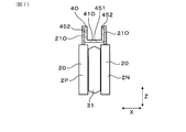
- FIG. 1 is a plan view of a power conversion device according to a first embodiment
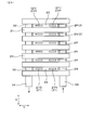
- FIG. 2 is a circuit diagram of the power conversion device in the first embodiment
- FIG. 3 is a perspective view of a semiconductor module and a bus bar in Embodiment 1
- FIG. 4 is a cross-sectional view of the semiconductor module and the coexistence and placement unit in the first embodiment
- 5 is a cross-sectional view taken along line VV of FIG. 6
- FIG. 7 is a cross-sectional view of the semiconductor module and the output interposed portion in the first embodiment
- FIG. 8 is a plan view of the power conversion device in a state in which the bus bar is removed in the first embodiment
- FIG. 9 is a cross-sectional view of the semiconductor module and the coexistence / arrangement portion in the second embodiment
- FIG. 10 is a cross-sectional view of a semiconductor module and a coexistence arrangement portion in the third embodiment
- FIG. 11 is a cross-sectional view of the semiconductor module and the coexistence / disposition portion in the fourth embodiment
- FIG. 12 is a circuit diagram of the power conversion device in the fifth embodiment.
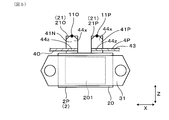
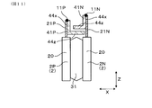
- the power conversion device 1 of the present embodiment is a switching circuit unit including a plurality of upper arm switching elements 20 u connected to the positive electrode wiring and a plurality of lower arm switching elements 20 d connected to the negative electrode wiring. It is equipped with 101.
- the power conversion device 1 has a plurality of bus bars 4 and a plurality of semiconductor modules 2 formed by projecting the power terminals 21 from the module body 20.
- the power conversion device 1 includes, as the bus bars 4, a positive electrode bus bar 4P that configures positive electrode wiring and a negative electrode bus bar 4N that configures negative electrode wiring.
- the power conversion device 1 includes a first semiconductor module 2P and a second semiconductor module 2N as the semiconductor module 2.
- the first semiconductor module 2P incorporates an upper arm switching element 20u.
- the first semiconductor module 2P also includes a positive terminal 21P, which is a power terminal 21 connected to the positive bus bar 4P.
- the second semiconductor module 2N incorporates the lower arm switching element 20d.
- the second semiconductor module 2N also includes a negative terminal 21N that is a power terminal 21 connected to the negative bus bar 4N.
- the first semiconductor module 2P and the second semiconductor module 2N are disposed in a state in which the positive electrode terminal 21P and the negative electrode terminal 21N are opposed in the direction orthogonal to the projecting direction.
- the positive electrode bus bar 4P and the negative electrode bus bar 4N each have coexistence placement portions 41P and 41N.
- the coexistence placement portions 41P and 41N are portions disposed between the positive electrode terminal 21P and the negative electrode terminal 21N when viewed from the projecting direction of the power terminal 21 as shown in FIG. At least a portion of the coexistence / arrangement portions 41P and 41N is disposed in the space between the positive electrode terminal 21P and the negative electrode terminal 21N.
- the coexistence / arrangement portions 41P and 41N are entirely disposed in the space between the positive electrode terminal 21P and the negative electrode terminal 21N.
- a direction parallel to the protruding direction of the power terminal 21 is referred to as the Z direction as appropriate.
- the direction in which the positive electrode terminal 21P and the negative electrode terminal 21N face each other is referred to as the X direction as appropriate.
- a direction orthogonal to both the X direction and the Z direction is referred to as a Y direction as appropriate.
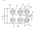
- the power conversion device 1 of the present embodiment is, for example, an inverter mounted on a vehicle. Then, as shown in FIG. 2, power conversion between DC power and AC power is performed between the DC power supply 51 and the three-phase AC rotating electrical machine 52.
- the switching circuit unit 101 of the power conversion device 1 includes three-phase legs. That is, the three-phase legs are connected in parallel with each other between the positive electrode wiring connected to the positive electrode of the DC power supply 51 and the negative electrode wiring connected to the negative electrode of the DC power supply 51.
- Each leg is formed of an upper arm switching element 20 u and a lower arm switching element 20 d connected in series with each other.
- connection point between the upper arm switching element 20 u and the lower arm switching element 20 d in each leg is connected to the three electrodes of the rotary electric machine 52 via the output wiring. Further, a capacitor 53 is connected between the DC power supply 51 and the switching circuit unit 101 so as to suspend the positive electrode wire and the negative electrode wire. In addition, flywheel diodes are connected in reverse parallel to the respective switching elements.
- the switching element can be formed of an IGBT.
- IGBT is an abbreviation for Insulated Gate Bipolar Transistor, that is, an insulated gate bipolar transistor.
- the switching element can also be a MOSFET.
- MOSFET is an abbreviation for Metal Oxide Semiconductor Field Effect Transistor, or metal oxide field effect transistor.
- the positive electrode wiring is configured by the positive electrode bus bar 4P.
- the negative electrode wiring is configured by the negative electrode bus bar 4N.
- the output wiring is configured by the output bus bar 4O.
- Each semiconductor module 2 has two power terminals 21. As shown in FIG. 5, the first semiconductor module 2P has, as the power terminal 21, a positive electrode terminal 21P and an output terminal 21O. As shown in FIG. 6, the second semiconductor module 2N has, as a power terminal 21, a negative electrode terminal 21N and an output terminal 21O.
- the upper arm switching elements 20 u and the lower arm switching elements 20 d are respectively incorporated in the individual semiconductor modules 2.
- one upper arm switching element 20u is incorporated in one first semiconductor module 2P
- one lower arm switching element 20d is incorporated in one second semiconductor module 2N.
- the positive electrode terminal 21P is at the same potential as the collector of the upper arm switching element 20u
- the output terminal 21O is at the same potential as the emitter of the upper arm switching element 20u
- the output terminal 21O is at the same potential as the collector of the lower arm switching element 20d
- the negative terminal 21N is at the same potential as the emitter of the lower arm switching element 20d.
- Each semiconductor module 2 projects two power terminals 21 from the module body 20 in the same direction as the Z direction. Moreover, although illustration is abbreviate
- the module main body 20 exposes the heat sink 201 on both main surfaces thereof.
- the first semiconductor module 2P and the second semiconductor module 2N are disposed such that the heat dissipation plates 201 face each other.
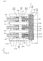
- the plurality of semiconductor modules 2 are stacked in the X direction together with the plurality of cooling pipes 31 so that the first semiconductor modules 2P and the second semiconductor modules 2N are alternately arranged.
- the cooling pipe 31 is disposed so as to be in thermal contact with the heat dissipation plate 201 of the semiconductor module 2.
- the cooling pipe 31 is provided with a refrigerant flow path through which the refrigerant flows.
- the cooling pipes 31 adjacent to each other in the X direction are connected by the connecting pipe 32 in the vicinity of both ends in the Y direction. Further, the cooling pipe 31 disposed at one end in the X direction is provided with a refrigerant introduction pipe 33 for introducing the refrigerant and a refrigerant discharge pipe 34 for discharging the refrigerant.
- the cooling pipe 31 is made of a metal having excellent thermal conductivity, such as an aluminum alloy.
- the power terminal 21 of the semiconductor module 2 protrudes further than the cooling pipe 31 in the Z direction. The power terminals 21 of the plurality of semiconductor modules 2 project to the same side in the Z direction.
- a capacitor 53 is disposed on one side in the Y direction with respect to the stacked portion of the semiconductor module 2.
- the two power terminals 21 in each semiconductor module 2 are provided with the positive electrode terminal 21P or the negative electrode terminal 21N closer to the capacitor 53 than the output terminal 21O in the Y direction.
- An output bus bar 4O is connected to the output terminal 21O.
- Each output bus bar 4O is connected to both the output terminals 21O of the first semiconductor module 2P and the second semiconductor module 2N adjacent in the X direction.
- the output bus bar 4O is formed to extend in the lateral direction Y from the connection with the output terminal 21O.
- a positive bus bar 4P and a negative bus bar 4N are disposed so as to connect the positive electrode and the negative electrode of the capacitor 53 to the power terminal 21 of the semiconductor module 2.
- the positive electrode bus bar 4P and the negative electrode bus bar 4N are integrated with the capacitor 53.
- Positive electrode bus bar 4P and negative electrode bus bar 4N each have main body plate portion 42 disposed so as to overlap each other in the Z direction, and a plurality of branch portions 43 extending from main body plate portion 42 to power terminal 21 in the Y direction. . A part of this branch part 43 becomes the above-mentioned coexistence arrangement parts 41P and 41N.
- Each branch portion 43 is connected to one positive terminal 21P and one negative terminal 21N adjacent in the X direction. Then, counting from one end in the X direction, between the semiconductor modules 2 of the first and second stages, between the semiconductor modules 2 of the third and fourth stages, and the fifth and sixth stages
- the coexistence placement units 41P and 41N are disposed between the semiconductor modules 2 of FIG. That is, between the power terminals 21 adjacent to each other in the X direction, there are portions where the coexistence / arrangement portions 41P and 41N are disposed and portions where the coexistence / disposition portions 41P and 41N are not disposed.
- the coexistence / arrangement portions 41P and 41N have opposing portions arranged so that the main surfaces thereof face each other.
- the coexistence / arrangement portions 41P and 41N have, as opposing portions, an array opposing portion 44x that opposes the array direction of the positive electrode terminal 21P and the negative electrode terminal 21N, that is, the X direction.
- the coexistence / arrangement portions 41P and 41N have, as opposing portions, a projecting opposing portion 44z opposing in the projecting direction of the power terminal 21, that is, the Z direction. That is, in the present embodiment, the coexistence / arrangement parts 41P and 41N have both the line opposing part 44x and the protruding opposing part 44z as the opposing part.
- the coexistence placement units 41P and 41N are substantially L-shaped in a cross section orthogonal to the Y direction.
- the coexistence placement portions 41P and 41N are formed by bending one end edge in the X direction of the end portions of the branch portions 43 of the bus bars 4 in one of the Z directions.
- a portion standing in the Z direction is the line facing portion 44 x, and a protruding facing portion 44 z is formed in a portion of the branch portion 43 where the main surface is directed in the Z direction.
- the erecting direction of the row opposing portion 44x from the projecting opposing portion 44z is the same as the projecting direction of the power terminal 21.
- the distance d1 between the pair of coexistence portions 41P and 41N in the protrusion facing portion 44z is smaller than the distance d2 between the pair of coexistence portions 41P and 41N in the row facing portion 44x.
- the distance between the protrusion opposing portion 44z of the coexistence arrangement portion 41P in the positive electrode bus bar 4P and the protrusion opposing portion 44z of the coexistence arrangement portion 41N in the negative electrode bus bar 4N is a distance d1.
- the distance between the alignment facing portion 44x of the coexistence arranging portion 41P in the positive electrode bus bar 4P and the alignment opposing portion 44x of the coexistence arranging portion 41N in the negative electrode bus bar 4N is a distance d2.
- these intervals d1 and d2 have a relation of d2> d1.
- the length L1 of the protrusion facing portion 44z in the direction in which the positive electrode terminal 21P and the negative electrode terminal 21N are aligned, ie, the X direction, is longer than the length L2 of the row facing portion 44x in the protruding direction of the power terminal 21, ie, the Z direction. .
- the coexistence placement part in which the protruding facing part 44z is disposed closer to the module main body 20 has the protruding facing part 44z in the module body than the connection part with the power terminal 21. It is placed near 20.
- the protrusion opposing portion 44 z is disposed at a position closer to the module main body 20 in the coexistence arrangement portion 41 P of the positive electrode bus bar 4 P. Therefore, the protrusion opposing portion 44z of the coexistence arrangement portion 41P of the positive electrode bus bar 4P is disposed at a position closer to the module body 20 than the connection portion 11P.
- each of the bus bars 4 the row facing portion 44 x is superimposed on the power terminal 21 in the X direction.
- the end portions of the power terminals 21 and the end portions of the opposing portions 44x are welded to each other.
- the welded portions become the connection portions 11P and 11N.
- laser welding can be used.
- connection portion 11P between the positive electrode bus bar 4P and the positive electrode terminal 21P in the colocated portion 41P, 41N and the connection portion 11N between the negative bus bar 4N and the negative terminal 21N in the colocated portion 41P, 41N have the same position in the Z direction. is there.
- the positions in the Z direction are equal, for example, the difference in the position in the Z direction between the connection portion 11P and the connection portion 11N can be approximately equal to or less than the thickness of the bus bar 4.
- the output intervening portion 41O and the coexistence placement portions 41P and 41N disposed between the adjacent first semiconductor module 2P and the second semiconductor module 2N are the respective power terminals 21 and
- the connection portions 11O, 11P, and 11N are disposed at equivalent positions in the Z direction.
- the output intervening portion 41O has a substrate portion 451 having a main surface facing in the Z direction, and a pair of standing portions 452 rising from the substrate portion 451 in the protruding direction of the power terminal 21.
- the distance between the substrate 451 and the module body 20 is shorter than the distance between the substrate 451 and the tip of the output terminal 21O in the Z direction.
- the positive electrode bus bar 4P and the negative electrode bus bar 4N respectively have coexistence placement portions 41P and 41N. And, at least a part of the coexistence / arrangement portions 41P and 41N are arranged to coexist in the space between the positive electrode terminal 21P and the negative electrode terminal 21N which are arranged to be opposed to each other. With this configuration, the positive electrode bus bar 4P and the negative electrode bus bar 4N are closely arranged in the coexistence arrangement portions 41P and 41N. As a result, the inductance in bus bar 4 can be reduced.
- the coexistence placement units 41P and 41N have facing portions 44x and 44z. Thus, currents in opposite directions flow through the facing portions of the positive electrode bus bar 4P and the negative electrode bus bar 4N. Therefore, the inductance can be more effectively reduced by arranging them to face each other.
- the coexistence / arrangement portions 41P and 41N have a row opposing portion 44x as the opposing portion.
- the bus bars 4 can be easily connected to the power terminals 21 in the row facing portion 44 x.
- the coexistence / arrangement portions 41P and 41N have a projecting opposing portion 44z as the opposing portion.
- the coexistence / arrangement portions 41P and 41N can be easily arranged close to each other over a wide area. Therefore, it is easier to reduce the inductance.
- both the line facing portion 44x and the protruding facing portion 44z are provided.
- the above two effects can be obtained simultaneously. That is, the connection structure between the bus bar 4 and the power terminal 21 can be simplified, and the reduction of the inductance can be effectively achieved.
- the distance d1 between the pair of coexistence portions 41P and 41N in the protrusion facing portion 44z is smaller than the distance d2 between the pair of coexistence portions 41P and 41N in the row facing portion 44x.
- the length L1 of the projecting facing portion 44z in the X direction is longer than the length L2 of the line facing portion 44x in the Z direction.
- the current loop formed by the switching element and the internal wiring inside the module main body portion 20, the coexistence placement portion 41P, and the power terminal 21 can be reduced.
- the inductance can be reduced.
- a cooling pipe 31 is interposed between the first semiconductor module 2P and the second semiconductor module 2N which are disposed adjacent to each other. Thereby, the semiconductor module 2 can be cooled effectively. Further, by interposing the cooling pipe 31, the coexistence placement parts 41P and 41N are disposed in the dead space formed between the power terminals 21 in the X direction. Therefore, in particular, the arrangement of the coexistence placement units 41P and 41N does not prevent the miniaturization of the power conversion device 1.
- the protrusion facing portion 44z is disposed at a position farther from the module main body 20 than the connection portion for one of the pair of coexistence / arrangement portions 41P and 41N.
- the protruding facing portion 44z is arranged at a position farther from the module main body portion 20 than the connection portion 11N.
- the protruding opposing portion 44z of the negative electrode bus bar 4N is disposed at a position farther from the module body 20 than the tip of the negative electrode terminal 21N.
- the coexistence arrangement portion 41N arranges the row facing portion 44x closer to the module body portion 20 than the protruding facing portion 44z.
- the protrusion facing portion 44z is arranged closer to the module body 20 than the connection portion 11P. That is, the coexistence arrangement portion 41P, in which the protrusion facing portion 44z is disposed closer to the module body portion 20, of the pair of coexistence arrangement portions 41P and 41N, is closer to the module body portion than the connection portion 11P. It is placed near 20. This point is the same as that of the first embodiment.
- the pair of coexistence / arrangement portions 41P and 41N arrange a part of each between the pair of power terminals 21. This can reduce the inductance. Further, the pair of coexistence / arrangement portions 41P and 41N have a row opposing portion 44x and a projecting opposing portion 44z. Thereby, the inductance can be effectively reduced.
- the coexistence arrangement portion of the positive electrode bus bar is disposed closer to the module main portion than the coexistence arrangement portion of the negative electrode bus bar, but this positional relationship is particularly limited. is not. That is, the coexistence arrangement portion of the negative electrode bus bar may be disposed closer to the module main body than the coexistence arrangement portion of the positive electrode bus bar.
- the pair of coexistence placement units may be disposed so as to have the same distance from the module main body.
Abstract
A power conversion device (1) has a positive electrode bus bar (4P), and a negative electrode bus bar (4N). The power conversion device (1) has: a first semiconductor module (2P), which has a built-in upper arm switching element (20u), and which is provided with a positive electrode terminal (21P); and a second semiconductor module (2N), which has a built-in lower arm switching element (20d), and which is provided with a negative electrode terminal (21N). The first semiconductor module (2P) and the second semiconductor module (2N) are disposed in a state wherein the positive electrode terminal (21P) and the negative electrode terminal (21N) face each other in the direction orthogonal to the protruding direction. When viewed from the protruding direction of a power terminal (21), the positive electrode bus bar (4P) and the negative electrode bus bar (4N) respectively have co-disposed sections (41P, 41N) that are disposed between the positive electrode terminal (21P) and the negative electrode terminal (21N). At least a part of each of the co-disposed sections (41P, 41N) is disposed in a space between the positive electrode terminal (21P) and the negative electrode terminal (21N).
Description
本出願は、2017年8月9日に出願された日本出願番号2017-154398号に基づくもので、ここにその記載内容を援用する。
This application is based on Japanese Patent Application No. 2017-154398 filed on Aug. 9, 2017, the contents of which are incorporated herein by reference.
本開示は、複数の半導体モジュールを備えた電力変換装置に関する。
The present disclosure relates to a power converter including a plurality of semiconductor modules.
上アームスイッチング素子を内蔵した半導体モジュールと、下アームスイッチング素子を内蔵した半導体モジュールとを、隣り合うように配置した電力変換装置が、特許文献1に開示されている。この電力変換装置においては、正極バスバーに接続される、上アームの半導体モジュールの正極端子と、負極バスバーに接続される、下アームの半導体モジュールの負極端子とが、隣り合って配置されている。
Patent Document 1 discloses a power conversion device in which a semiconductor module containing an upper arm switching element and a semiconductor module containing a lower arm switching element are arranged adjacent to each other. In this power conversion device, the positive electrode terminal of the upper arm semiconductor module connected to the positive electrode bus bar and the negative electrode terminal of the lower arm semiconductor module connected to the negative electrode bus bar are arranged adjacent to each other.
正極バスバーは、正極端子に接続される端子を突出してなる。また、負極バスバーは、負極端子と接続される端子を突出してなる。これらの端子は、隣り合う正極端子と負極端子との間に、それぞれ1本ずつ個別に配置されている。
The positive electrode bus bar protrudes from a terminal connected to the positive electrode terminal. In addition, the negative electrode bus bar projects a terminal connected to the negative electrode terminal. One each of these terminals is separately arrange | positioned between the positive electrode terminal which adjoins, and a negative electrode terminal.
上記のような、正極バスバーの端子及び負極バスバーの端子の配置構成の場合、各端子部分におけるインダクタンスを充分に低減することが困難である。特に、近年、電力変換装置において求められるスイッチング損失の低減に伴い、高速スイッチングが求められている。そうすると、バスバーにおけるインダクタンスの低減が求められる。このように、バスバー及びこれに接続される半導体モジュールとの接続部におけるインダクタンスの低減は、重要課題の一つとなっている。
In the case of the arrangement configuration of the terminal of the positive electrode bus bar and the terminal of the negative electrode bus bar as described above, it is difficult to sufficiently reduce the inductance at each terminal portion. In particular, in recent years, high-speed switching has been required along with the reduction of switching loss required for power converters. Then, reduction of the inductance in the bus bar is required. As described above, the reduction of the inductance at the connecting portion between the bus bar and the semiconductor module connected thereto is one of the important issues.
本開示は、インダクタンスを低減しやすい電力変換装置を提供しようとするものである。
The present disclosure seeks to provide a power converter that is easy to reduce the inductance.
本開示の一態様は、正極配線に接続される複数の上アームスイッチング素子と、負極配線に接続される複数の下アームスイッチング素子とを有するスイッチング回路部を備えた電力変換装置であって、
複数のバスバーと、
モジュール本体部からパワー端子を突出してなる複数の半導体モジュールと、を有し、
上記バスバーとして、上記正極配線を構成する正極バスバーと、上記負極配線を構成する負極バスバーと、を有し、
上記半導体モジュールとして、上記上アームスイッチング素子を内蔵すると共に上記正極バスバーに接続される上記パワー端子である正極端子を備えた第1半導体モジュールと、上記下アームスイッチング素子を内蔵すると共に上記負極バスバーに接続される上記パワー端子である負極端子を備えた第2半導体モジュールと、を有し、
上記第1半導体モジュールと上記第2半導体モジュールとは、上記正極端子と上記負極端子とを突出方向に直交する方向に対向させた状態で、配置されており、
上記正極バスバー及び上記負極バスバーは、上記パワー端子の突出方向から見たとき、共に上記正極端子と上記負極端子との間に配される共存配置部をそれぞれ有し、
上記共存配置部の少なくとも一部は、上記正極端子と上記負極端子との間の空間に配されている、電力変換装置にある。 One aspect of the present disclosure is a power conversion device including a switching circuit unit including a plurality of upper arm switching elements connected to a positive electrode wire and a plurality of lower arm switching elements connected to a negative electrode wire,
With multiple bus bars,
And a plurality of semiconductor modules formed by projecting power terminals from the module main body,
As the bus bar, it has a positive electrode bus bar which constitutes the positive electrode wire and a negative electrode bus bar which constitutes the negative electrode wire,
As the semiconductor module, a first semiconductor module including the positive arm terminal which is the power terminal connected to the positive bus bar while incorporating the upper arm switching element, the lower arm switching element and the negative bus bar. A second semiconductor module provided with a negative electrode terminal which is the power terminal to be connected;
The first semiconductor module and the second semiconductor module are disposed in a state in which the positive electrode terminal and the negative electrode terminal are opposed to each other in a direction orthogonal to the protruding direction,
The positive electrode bus bar and the negative electrode bus bar both have coexistence arrangement parts disposed between the positive electrode terminal and the negative electrode terminal when viewed from the projecting direction of the power terminal,
At least a part of the coexistence / arrangement portion is in the power conversion device disposed in the space between the positive electrode terminal and the negative electrode terminal.
上記電力変換装置においては、上記正極バスバーと上記負極バスバーとが、それぞれ上記共存配置部を有する。そして、共存配置部の少なくとも一部が、互いに対向配置された正極端子と負極端子との間の空間に共存するように配置されている。かかる構成により、正極バスバーと負極バスバーとが、共存配置部において近接配置されることとなる。その結果、バスバーにおけるインダクタンスを低減することができる。
In the power converter, the positive electrode bus bar and the negative electrode bus bar each have the coexistence arrangement portion. And, at least a part of the coexistence arrangement portion is arranged to coexist in the space between the positive electrode terminal and the negative electrode terminal arranged to face each other. According to this configuration, the positive electrode bus bar and the negative electrode bus bar are closely arranged in the coexistence arrangement portion. As a result, the inductance in the bus bar can be reduced.
以上のごとく、上記態様によれば、インダクタンスを低減しやすい電力変換装置を提供することができる。
As described above, according to the above aspect, it is possible to provide a power conversion device that can easily reduce the inductance.
本開示についての上記目的およびその他の目的、特徴や利点は、添付の図面を参照しながら下記の詳細な記述により、より明確になる。その図面は、
図1は、実施形態1における、電力変換装置の平面図であり、
図2は、実施形態1における、電力変換装置の回路図であり、
図3は、実施形態1における、半導体モジュールとバスバーの斜視図であり、
図4は、実施形態1における、半導体モジュールと共存配置部の断面図であり、
図5は、図4のV-V線矢視断面図であり、
図6は、図4のVI-VI線矢視断面図であり、
図7は、実施形態1における、半導体モジュールと出力介在部の断面図であり、
図8は、実施形態1における、バスバーを取り除いた状態の電力変換装置の平面図であり、
図9は、実施形態2における、半導体モジュールと共存配置部の断面図であり、
図10は、実施形態3における、半導体モジュールと共存配置部の断面図であり、
図11は、実施形態4における、半導体モジュールと共存配置部の断面図であり、
図12は、実施形態5における、電力変換装置の回路図である。
The above object and other objects, features and advantages of the present disclosure will become more apparent from the following detailed description with reference to the attached drawings. The drawing is
FIG. 1 is a plan view of a power conversion device according to a first embodiment, FIG. 2 is a circuit diagram of the power conversion device in the first embodiment, FIG. 3 is a perspective view of a semiconductor module and a bus bar in Embodiment 1; FIG. 4 is a cross-sectional view of the semiconductor module and the coexistence and placement unit in the first embodiment, 5 is a cross-sectional view taken along line VV of FIG. 6 is a cross-sectional view taken along line VI-VI of FIG. 7 is a cross-sectional view of the semiconductor module and the output interposed portion in the first embodiment, FIG. 8 is a plan view of the power conversion device in a state in which the bus bar is removed in the first embodiment, FIG. 9 is a cross-sectional view of the semiconductor module and the coexistence / arrangement portion in the second embodiment, FIG. 10 is a cross-sectional view of a semiconductor module and a coexistence arrangement portion in the third embodiment, FIG. 11 is a cross-sectional view of the semiconductor module and the coexistence / disposition portion in the fourth embodiment, FIG. 12 is a circuit diagram of the power conversion device in the fifth embodiment.
(実施形態1)
電力変換装置に係る実施形態について、図1~図8を参照して説明する。
本実施形態の電力変換装置1は、図2に示すごとく、正極配線に接続される複数の上アームスイッチング素子20uと、負極配線に接続される複数の下アームスイッチング素子20dとを有するスイッチング回路部101を備えたものである。 (Embodiment 1)
Embodiments of the power converter will be described with reference to FIGS. 1 to 8.
As shown in FIG. 2, thepower conversion device 1 of the present embodiment is a switching circuit unit including a plurality of upper arm switching elements 20 u connected to the positive electrode wiring and a plurality of lower arm switching elements 20 d connected to the negative electrode wiring. It is equipped with 101.
電力変換装置に係る実施形態について、図1~図8を参照して説明する。
本実施形態の電力変換装置1は、図2に示すごとく、正極配線に接続される複数の上アームスイッチング素子20uと、負極配線に接続される複数の下アームスイッチング素子20dとを有するスイッチング回路部101を備えたものである。 (Embodiment 1)
Embodiments of the power converter will be described with reference to FIGS. 1 to 8.
As shown in FIG. 2, the
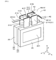
電力変換装置1は、図1に示すごとく、複数のバスバー4と、モジュール本体部20からパワー端子21を突出してなる複数の半導体モジュール2と、を有する。
電力変換装置1は、バスバー4として、正極配線を構成する正極バスバー4Pと、負極配線を構成する負極バスバー4Nと、を有する。
電力変換装置1は、半導体モジュール2として、第1半導体モジュール2Pと、第2半導体モジュール2Nと、を有する。 As shown in FIG. 1, thepower conversion device 1 has a plurality of bus bars 4 and a plurality of semiconductor modules 2 formed by projecting the power terminals 21 from the module body 20.
Thepower conversion device 1 includes, as the bus bars 4, a positive electrode bus bar 4P that configures positive electrode wiring and a negative electrode bus bar 4N that configures negative electrode wiring.
Thepower conversion device 1 includes a first semiconductor module 2P and a second semiconductor module 2N as the semiconductor module 2.
電力変換装置1は、バスバー4として、正極配線を構成する正極バスバー4Pと、負極配線を構成する負極バスバー4Nと、を有する。
電力変換装置1は、半導体モジュール2として、第1半導体モジュール2Pと、第2半導体モジュール2Nと、を有する。 As shown in FIG. 1, the
The
The
図2~図5に示すごとく、第1半導体モジュール2Pは、上アームスイッチング素子20uを内蔵している。また、第1半導体モジュール2Pは、正極バスバー4Pに接続されるパワー端子21である正極端子21Pを備えている。図2~図4、図6に示すごとく、第2半導体モジュール2Nは、下アームスイッチング素子20dを内蔵している。また、第2半導体モジュール2Nは、負極バスバー4Nに接続されるパワー端子21である負極端子21Nを備えている。
As shown in FIGS. 2 to 5, the first semiconductor module 2P incorporates an upper arm switching element 20u. The first semiconductor module 2P also includes a positive terminal 21P, which is a power terminal 21 connected to the positive bus bar 4P. As shown in FIG. 2 to FIG. 4 and FIG. 6, the second semiconductor module 2N incorporates the lower arm switching element 20d. The second semiconductor module 2N also includes a negative terminal 21N that is a power terminal 21 connected to the negative bus bar 4N.
図3、図4に示すごとく、第1半導体モジュール2Pと第2半導体モジュール2Nとは、正極端子21Pと負極端子21Nとを突出方向に直交する方向に対向させた状態で、配置されている。
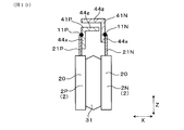
正極バスバー4P及び負極バスバー4Nは、共存配置部41P、41Nをそれぞれ有する。共存配置部41P、41Nは、図1に示すごとく、パワー端子21の突出方向から見たとき、共に正極端子21Pと負極端子21Nとの間に配される部位である。
共存配置部41P、41Nの少なくとも一部は、正極端子21Pと負極端子21Nとの間の空間に配されている。特に、本実施形態においては、共存配置部41P、41Nは、その全体が、正極端子21Pと負極端子21Nとの間の空間に配されている。 As shown in FIGS. 3 and 4, thefirst semiconductor module 2P and the second semiconductor module 2N are disposed in a state in which the positive electrode terminal 21P and the negative electrode terminal 21N are opposed in the direction orthogonal to the projecting direction.
The positiveelectrode bus bar 4P and the negative electrode bus bar 4N each have coexistence placement portions 41P and 41N. The coexistence placement portions 41P and 41N are portions disposed between the positive electrode terminal 21P and the negative electrode terminal 21N when viewed from the projecting direction of the power terminal 21 as shown in FIG.
At least a portion of the coexistence / arrangement portions 41P and 41N is disposed in the space between the positive electrode terminal 21P and the negative electrode terminal 21N. In particular, in the present embodiment, the coexistence / arrangement portions 41P and 41N are entirely disposed in the space between the positive electrode terminal 21P and the negative electrode terminal 21N.
正極バスバー4P及び負極バスバー4Nは、共存配置部41P、41Nをそれぞれ有する。共存配置部41P、41Nは、図1に示すごとく、パワー端子21の突出方向から見たとき、共に正極端子21Pと負極端子21Nとの間に配される部位である。
共存配置部41P、41Nの少なくとも一部は、正極端子21Pと負極端子21Nとの間の空間に配されている。特に、本実施形態においては、共存配置部41P、41Nは、その全体が、正極端子21Pと負極端子21Nとの間の空間に配されている。 As shown in FIGS. 3 and 4, the
The positive
At least a portion of the coexistence /
なお、以下において、パワー端子21の突出方向に平行な方向を、適宜、Z方向という。また、正極端子21Pと負極端子21Nとが対向する方向を、適宜、X方向という。また、X方向とZ方向との双方に直交する方向を、適宜、Y方向というものとする。
In the following, a direction parallel to the protruding direction of the power terminal 21 is referred to as the Z direction as appropriate. Further, the direction in which the positive electrode terminal 21P and the negative electrode terminal 21N face each other is referred to as the X direction as appropriate. In addition, a direction orthogonal to both the X direction and the Z direction is referred to as a Y direction as appropriate.
本実施形態の電力変換装置1は、例えば、車両に搭載されるインバータである。そして、図2に示すごとく、直流電源51と三相交流の回転電機52との間において、直流電力と交流電力との電力変換を行う。電力変換装置1のスイッチング回路部101は、3相のレグを備える。すなわち、3相のレグは、直流電源51の正極に接続される正極配線と、直流電源51の負極に接続される負極配線との間に、互いに並列に接続されている。各レグは、互いに直列接続された上アームスイッチング素子20uと下アームスイッチング素子20dとによって形成されている。
The power conversion device 1 of the present embodiment is, for example, an inverter mounted on a vehicle. Then, as shown in FIG. 2, power conversion between DC power and AC power is performed between the DC power supply 51 and the three-phase AC rotating electrical machine 52. The switching circuit unit 101 of the power conversion device 1 includes three-phase legs. That is, the three-phase legs are connected in parallel with each other between the positive electrode wiring connected to the positive electrode of the DC power supply 51 and the negative electrode wiring connected to the negative electrode of the DC power supply 51. Each leg is formed of an upper arm switching element 20 u and a lower arm switching element 20 d connected in series with each other.
そして、各レグにおける、上アームスイッチング素子20uと下アームスイッチング素子20dとの接続点が、それぞれ出力配線を介して、回転電機52の3つの電極に接続されている。また、直流電源51とスイッチング回路部101との間において、正極配線と負極配線とを懸架するように、コンデンサ53が接続されている。また、各スイッチング素子には、フライホイールダイオードが逆並列接続されている。
The connection point between the upper arm switching element 20 u and the lower arm switching element 20 d in each leg is connected to the three electrodes of the rotary electric machine 52 via the output wiring. Further, a capacitor 53 is connected between the DC power supply 51 and the switching circuit unit 101 so as to suspend the positive electrode wire and the negative electrode wire. In addition, flywheel diodes are connected in reverse parallel to the respective switching elements.
なお、スイッチング素子は、IGBTにて構成することができる。ここで、IGBTは、Insulated Gate Bipolar Transistor、すなわち、絶縁ゲートバイポーラトランジスタの略である。また、スイッチング素子は、MOSFETとすることもできる。MOSFETは、Metal Oxide Semiconductor Field Effect Transistor、すなわち、金属酸化物電界効果トランジスタの略である。
The switching element can be formed of an IGBT. Here, IGBT is an abbreviation for Insulated Gate Bipolar Transistor, that is, an insulated gate bipolar transistor. The switching element can also be a MOSFET. MOSFET is an abbreviation for Metal Oxide Semiconductor Field Effect Transistor, or metal oxide field effect transistor.
上述のように、正極配線は、正極バスバー4Pによって構成されている。負極配線は、負極バスバー4Nによって構成されている。また、出力配線は、出力バスバー4Oによって構成されている。
各半導体モジュール2は、2本のパワー端子21を有する。図5に示すごとく、第1半導体モジュール2Pは、パワー端子21として、正極端子21Pと出力端子21Oとを有する。図6に示すごとく、第2半導体モジュール2Nは、パワー端子21として、負極端子21Nと出力端子21Oとを有する。 As described above, the positive electrode wiring is configured by the positiveelectrode bus bar 4P. The negative electrode wiring is configured by the negative electrode bus bar 4N. Also, the output wiring is configured by the output bus bar 4O.
Eachsemiconductor module 2 has two power terminals 21. As shown in FIG. 5, the first semiconductor module 2P has, as the power terminal 21, a positive electrode terminal 21P and an output terminal 21O. As shown in FIG. 6, the second semiconductor module 2N has, as a power terminal 21, a negative electrode terminal 21N and an output terminal 21O.
各半導体モジュール2は、2本のパワー端子21を有する。図5に示すごとく、第1半導体モジュール2Pは、パワー端子21として、正極端子21Pと出力端子21Oとを有する。図6に示すごとく、第2半導体モジュール2Nは、パワー端子21として、負極端子21Nと出力端子21Oとを有する。 As described above, the positive electrode wiring is configured by the positive
Each
図2に示すごとく、各上アームスイッチング素子20u及び各下アームスイッチング素子20dが、それぞれ個別の半導体モジュール2に内蔵されている。特に本実施形態においては、一つの第1半導体モジュール2Pに一つの上アームスイッチング素子20uを内蔵し、一つの第2半導体モジュール2Nに一つの下アームスイッチング素子20dを内蔵している。
As shown in FIG. 2, the upper arm switching elements 20 u and the lower arm switching elements 20 d are respectively incorporated in the individual semiconductor modules 2. In the present embodiment, in particular, one upper arm switching element 20u is incorporated in one first semiconductor module 2P, and one lower arm switching element 20d is incorporated in one second semiconductor module 2N.
それゆえ、第1半導体モジュール2Pにおいて、正極端子21Pが、上アームスイッチング素子20uのコレクタと同電位であり、出力端子21Oが、上アームスイッチング素子20uのエミッタと同電位である。第2半導体モジュール2Nにおいて、出力端子21Oが、下アームスイッチング素子20dのコレクタと同電位であり、負極端子21Nが、下アームスイッチング素子20dのエミッタと同電位である。
Therefore, in the first semiconductor module 2P, the positive electrode terminal 21P is at the same potential as the collector of the upper arm switching element 20u, and the output terminal 21O is at the same potential as the emitter of the upper arm switching element 20u. In the second semiconductor module 2N, the output terminal 21O is at the same potential as the collector of the lower arm switching element 20d, and the negative terminal 21N is at the same potential as the emitter of the lower arm switching element 20d.
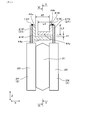
図3~図7に示すごとく、半導体モジュール2は、略直方体形状のモジュール本体部20を有する。モジュール本体部20は、他の面よりも面積の大きい一対の主面を備えている。この主面の法線方向に、複数の半導体モジュール2が積層されている(図8参照)。また、半導体モジュール2のパワー端子21は、略板状に形成されている。パワー端子21の主面は、モジュール本体部20の主面と略平行である。つまり、モジュール本体部20の主面も、パワー端子21の主面も、上述したX方向を向いている。
As shown in FIG. 3 to FIG. 7, the semiconductor module 2 has a module main body 20 having a substantially rectangular parallelepiped shape. The module main body 20 includes a pair of main surfaces having a larger area than the other surfaces. A plurality of semiconductor modules 2 are stacked in the normal direction of the main surface (see FIG. 8). Also, the power terminals 21 of the semiconductor module 2 are formed in a substantially plate shape. The main surface of the power terminal 21 is substantially parallel to the main surface of the module body 20. That is, both the main surface of the module main body 20 and the main surface of the power terminal 21 face the above-described X direction.
各半導体モジュール2は、2本のパワー端子21をモジュール本体部20から、Z方向の同じ方向に突出してなる。また、図示を省略するが、半導体モジュール2は、Z方向において、パワー端子21と反対側に、制御端子を突出させているものとすることができる。モジュール本体部20は、その両主面に、放熱板201を露出させている。第1半導体モジュール2Pと第2半導体モジュール2Nとは、放熱板201同士が対向するように配置されている。
Each semiconductor module 2 projects two power terminals 21 from the module body 20 in the same direction as the Z direction. Moreover, although illustration is abbreviate | omitted, the semiconductor module 2 can be made to project the control terminal on the opposite side to the power terminal 21 in the Z direction. The module main body 20 exposes the heat sink 201 on both main surfaces thereof. The first semiconductor module 2P and the second semiconductor module 2N are disposed such that the heat dissipation plates 201 face each other.
そして、図8に示すごとく、複数の半導体モジュール2は、第1半導体モジュール2Pと第2半導体モジュール2Nとが交互に並ぶように、複数の冷却管31と共にX方向に積層されている。冷却管31は、半導体モジュール2の放熱板201に熱的に接触するように、配置されている。
Then, as shown in FIG. 8, the plurality of semiconductor modules 2 are stacked in the X direction together with the plurality of cooling pipes 31 so that the first semiconductor modules 2P and the second semiconductor modules 2N are alternately arranged. The cooling pipe 31 is disposed so as to be in thermal contact with the heat dissipation plate 201 of the semiconductor module 2.
冷却管31は、内部に冷媒を流通させる冷媒流路を備えている。X方向に隣り合う冷却管31同士は、Y方向における両端部付近において、連結管32によって接続されている。また、X方向の一端に配された冷却管31には、冷媒を導入する冷媒導入管33と、冷媒を排出する冷媒排出管34とが設けてある。冷却管31は、アルミニウム合金等、熱伝導性に優れた金属によって構成されている。半導体モジュール2のパワー端子21は、Z方向において、冷却管31よりも突出している。複数の半導体モジュール2のパワー端子21は、Z方向における同じ側に突出している。
The cooling pipe 31 is provided with a refrigerant flow path through which the refrigerant flows. The cooling pipes 31 adjacent to each other in the X direction are connected by the connecting pipe 32 in the vicinity of both ends in the Y direction. Further, the cooling pipe 31 disposed at one end in the X direction is provided with a refrigerant introduction pipe 33 for introducing the refrigerant and a refrigerant discharge pipe 34 for discharging the refrigerant. The cooling pipe 31 is made of a metal having excellent thermal conductivity, such as an aluminum alloy. The power terminal 21 of the semiconductor module 2 protrudes further than the cooling pipe 31 in the Z direction. The power terminals 21 of the plurality of semiconductor modules 2 project to the same side in the Z direction.
図1に示すごとく、半導体モジュール2の積層部に対して、Y方向の一方側に、コンデンサ53が配置されている。各半導体モジュール2における2つのパワー端子21は、正極端子21P又は負極端子21Nを、Y方向において、出力端子21Oよりもコンデンサ53側に設けてある。
As shown in FIG. 1, a capacitor 53 is disposed on one side in the Y direction with respect to the stacked portion of the semiconductor module 2. The two power terminals 21 in each semiconductor module 2 are provided with the positive electrode terminal 21P or the negative electrode terminal 21N closer to the capacitor 53 than the output terminal 21O in the Y direction.
出力端子21Oには、出力バスバー4Oが接続される。各出力バスバー4Oは、X方向に隣り合う第1半導体モジュール2P及び第2半導体モジュール2Nの出力端子21Oの双方に接続されている。そして、出力バスバー4Oは、出力端子21Oとの接続部から、横方向Yに延びるように形成されている。
An output bus bar 4O is connected to the output terminal 21O. Each output bus bar 4O is connected to both the output terminals 21O of the first semiconductor module 2P and the second semiconductor module 2N adjacent in the X direction. The output bus bar 4O is formed to extend in the lateral direction Y from the connection with the output terminal 21O.
また、コンデンサ53の正極及び負極と、半導体モジュール2のパワー端子21とを接続するように、正極バスバー4P及び負極バスバー4Nが配されている。なお、正極バスバー4P及び負極バスバー4Nは、コンデンサ53と一体化されている。正極バスバー4P及び負極バスバー4Nは、それぞれ、Z方向に互いに重なるように配される本体板部42と、該本体板部42からY方向におけるパワー端子21側へ延びる複数の分岐部43とを有する。この分岐部43の一部が、上述の共存配置部41P、41Nとなる。
Further, a positive bus bar 4P and a negative bus bar 4N are disposed so as to connect the positive electrode and the negative electrode of the capacitor 53 to the power terminal 21 of the semiconductor module 2. The positive electrode bus bar 4P and the negative electrode bus bar 4N are integrated with the capacitor 53. Positive electrode bus bar 4P and negative electrode bus bar 4N each have main body plate portion 42 disposed so as to overlap each other in the Z direction, and a plurality of branch portions 43 extending from main body plate portion 42 to power terminal 21 in the Y direction. . A part of this branch part 43 becomes the above-mentioned coexistence arrangement parts 41P and 41N.
各分岐部43は、X方向に隣り合う一つの正極端子21Pと一つの負極端子21Nとに接続されている。そして、X方向の一方の端部から数えて、1段目と2段目の半導体モジュール2の間と、3段目と4段目の半導体モジュール2の間と、5段目と6段目の半導体モジュール2の間とに、それぞれ共存配置部41P、41Nが配される。すなわち、X方向に隣り合うパワー端子21の間には、共存配置部41P、41Nが配置される部分と、配置されない部分とがある。
Each branch portion 43 is connected to one positive terminal 21P and one negative terminal 21N adjacent in the X direction. Then, counting from one end in the X direction, between the semiconductor modules 2 of the first and second stages, between the semiconductor modules 2 of the third and fourth stages, and the fifth and sixth stages The coexistence placement units 41P and 41N are disposed between the semiconductor modules 2 of FIG. That is, between the power terminals 21 adjacent to each other in the X direction, there are portions where the coexistence / arrangement portions 41P and 41N are disposed and portions where the coexistence / disposition portions 41P and 41N are not disposed.
図4に示すごとく、共存配置部41P、41Nは、互いの主面が対向するように配置された対向部を有する。共存配置部41P、41Nは、対向部として、正極端子21Pと負極端子21Nとの並び方向、すなわちX方向に対向する並び対向部44xを有する。また、共存配置部41P、41Nは、対向部として、パワー端子21の突出方向、すなわちZ方向に対向する突出対向部44zを有する。つまり、本実施形態においては、共存配置部41P、41Nは、対向部として、並び対向部44xと突出対向部44zとの双方を有する。
As shown in FIG. 4, the coexistence / arrangement portions 41P and 41N have opposing portions arranged so that the main surfaces thereof face each other. The coexistence / arrangement portions 41P and 41N have, as opposing portions, an array opposing portion 44x that opposes the array direction of the positive electrode terminal 21P and the negative electrode terminal 21N, that is, the X direction. Further, the coexistence / arrangement portions 41P and 41N have, as opposing portions, a projecting opposing portion 44z opposing in the projecting direction of the power terminal 21, that is, the Z direction. That is, in the present embodiment, the coexistence / arrangement parts 41P and 41N have both the line opposing part 44x and the protruding opposing part 44z as the opposing part.
共存配置部41P、41Nは、Y方向に直交する断面において、略L字状となっている。共存配置部41P、41Nは、各バスバー4の分岐部43の先端部において、そのX方向の一方の端縁を、Z方向の一方へ屈曲させて形成されている。Z方向に立設した部分が、並び対向部44xとなり、分岐部43におけるZ方向に主面が向いた部分に、突出対向部44zが形成されている。突出対向部44zからの並び対向部44xの立設方向は、パワー端子21の突出方向と同じである。
The coexistence placement units 41P and 41N are substantially L-shaped in a cross section orthogonal to the Y direction. The coexistence placement portions 41P and 41N are formed by bending one end edge in the X direction of the end portions of the branch portions 43 of the bus bars 4 in one of the Z directions. A portion standing in the Z direction is the line facing portion 44 x, and a protruding facing portion 44 z is formed in a portion of the branch portion 43 where the main surface is directed in the Z direction. The erecting direction of the row opposing portion 44x from the projecting opposing portion 44z is the same as the projecting direction of the power terminal 21.
突出対向部44zにおける一対の共存配置部41P、41Nの間の間隔d1は、並び対向部44xにおける一対の共存配置部41P、41Nの間の間隔d2よりも小さい。正極バスバー4Pにおける共存配置部41Pの突出対向部44zと、負極バスバー4Nにおける共存配置部41Nの突出対向部44zとの間の間隔が、間隔d1である。また、正極バスバー4Pにおける共存配置部41Pの並び対向部44xと、負極バスバー4Nにおける共存配置部41Nの並び対向部44xとの間の間隔が、間隔d2である。そして、これらの間隔d1、d2が、d2>d1の関係を有する。
The distance d1 between the pair of coexistence portions 41P and 41N in the protrusion facing portion 44z is smaller than the distance d2 between the pair of coexistence portions 41P and 41N in the row facing portion 44x. The distance between the protrusion opposing portion 44z of the coexistence arrangement portion 41P in the positive electrode bus bar 4P and the protrusion opposing portion 44z of the coexistence arrangement portion 41N in the negative electrode bus bar 4N is a distance d1. Further, the distance between the alignment facing portion 44x of the coexistence arranging portion 41P in the positive electrode bus bar 4P and the alignment opposing portion 44x of the coexistence arranging portion 41N in the negative electrode bus bar 4N is a distance d2. And these intervals d1 and d2 have a relation of d2> d1.
また、正極端子21Pと負極端子21Nとの並び方向、すなわちX方向における突出対向部44zの長さL1は、パワー端子21の突出方向、すなわちZ方向における並び対向部44xの長さL2よりも長い。
Further, the length L1 of the protrusion facing portion 44z in the direction in which the positive electrode terminal 21P and the negative electrode terminal 21N are aligned, ie, the X direction, is longer than the length L2 of the row facing portion 44x in the protruding direction of the power terminal 21, ie, the Z direction. .
一対の共存配置部41P、41Nのうち、突出対向部44zがモジュール本体部20により近い側に配された共存配置部は、突出対向部44zを、パワー端子21との接続部よりもモジュール本体部20に近い位置に配置している。本実施形態においては、正極バスバー4Pの共存配置部41Pの方が、突出対向部44zをよりモジュール本体部20に近い位置に配置している。それゆえ、正極バスバー4Pの共存配置部41Pの突出対向部44zが、接続部11Pよりもモジュール本体部20に近い位置に配されている。
Of the pair of coexistence placement parts 41P and 41N, the coexistence placement part in which the protruding facing part 44z is disposed closer to the module main body 20 has the protruding facing part 44z in the module body than the connection part with the power terminal 21. It is placed near 20. In the present embodiment, the protrusion opposing portion 44 z is disposed at a position closer to the module main body 20 in the coexistence arrangement portion 41 P of the positive electrode bus bar 4 P. Therefore, the protrusion opposing portion 44z of the coexistence arrangement portion 41P of the positive electrode bus bar 4P is disposed at a position closer to the module body 20 than the connection portion 11P.
また、各バスバー4において、並び対向部44xがパワー端子21に対して、X方向に重ね合わせられている。そして、パワー端子21の先端部と並び対向部44xの先端部とにおいて、互いに溶接されている。この溶接部が、接続部11P、11Nとなる。溶接は、例えばレーザー溶接を用いることができる。
Further, in each of the bus bars 4, the row facing portion 44 x is superimposed on the power terminal 21 in the X direction. The end portions of the power terminals 21 and the end portions of the opposing portions 44x are welded to each other. The welded portions become the connection portions 11P and 11N. For welding, for example, laser welding can be used.
共存配置部41P、41Nにおける正極バスバー4Pと正極端子21Pとの接続部11Pと、共存配置部41P、41Nにおける負極バスバー4Nと負極端子21Nとの接続部11Nとは、Z方向における位置が同等である。ここで、Z方向における位置が同等とは、例えば、接続部11Pと接続部11NとのZ方向の位置の差が、バスバー4の厚み以下程度とすることができる。
The connection portion 11P between the positive electrode bus bar 4P and the positive electrode terminal 21P in the colocated portion 41P, 41N and the connection portion 11N between the negative bus bar 4N and the negative terminal 21N in the colocated portion 41P, 41N have the same position in the Z direction. is there. Here, if the positions in the Z direction are equal, for example, the difference in the position in the Z direction between the connection portion 11P and the connection portion 11N can be approximately equal to or less than the thickness of the bus bar 4.
図1、図7に示すごとく、第1半導体モジュール2Pと第2半導体モジュール2Nとは、互いの出力端子21O同士を対向配置させてなる。出力バスバー4Oは、対向配置された出力端子21O同士の間の空間に配される出力介在部41Oを有する。出力介在部41Oに、第1半導体モジュール2Pの出力端子21Oと第2半導体モジュール2Nの出力端子21Oとの双方が接続されている。
As shown in FIGS. 1 and 7, the first semiconductor module 2P and the second semiconductor module 2N are configured such that their output terminals 21O face each other. The output bus bar 4O has an output interposed portion 41O disposed in the space between the opposingly arranged output terminals 21O. Both the output terminal 21O of the first semiconductor module 2P and the output terminal 21O of the second semiconductor module 2N are connected to the output intervening portion 41O.
図5、図6に示すごとく、隣り合う第1半導体モジュール2Pと第2半導体モジュール2Nとの間に配された、出力介在部41Oと共存配置部41P、41Nとは、それぞれのパワー端子21との接続部11O、11P、11Nを、Z方向における同等の位置に有する。特に、すべてのパワー端子21とバスバー4との接続部11O、11P、11Nが、Z方向における同等の位置に配されていることが、より好ましい。
As shown in FIGS. 5 and 6, the output intervening portion 41O and the coexistence placement portions 41P and 41N disposed between the adjacent first semiconductor module 2P and the second semiconductor module 2N are the respective power terminals 21 and The connection portions 11O, 11P, and 11N are disposed at equivalent positions in the Z direction. In particular, it is more preferable that the connection portions 11O, 11P, 11N between all the power terminals 21 and the bus bars 4 be disposed at the same position in the Z direction.
出力介在部41Oは、Z方向を向く主面を有する基板部451と、基板部451からパワー端子21の突出方向に立ち上がる一対の立設部452とを有する。基板部451は、Z方向において、出力端子21Oの先端との距離よりもモジュール本体部20との距離の方が短い。
The output intervening portion 41O has a substrate portion 451 having a main surface facing in the Z direction, and a pair of standing portions 452 rising from the substrate portion 451 in the protruding direction of the power terminal 21. The distance between the substrate 451 and the module body 20 is shorter than the distance between the substrate 451 and the tip of the output terminal 21O in the Z direction.
次に、本実施形態の作用効果につき説明する。
上記電力変換装置1においては、図1、図3、図4に示すごとく、正極バスバー4Pと負極バスバー4Nとが、それぞれ共存配置部41P、41Nを有する。そして、共存配置部41P、41Nの少なくとも一部が、互いに対向配置された正極端子21Pと負極端子21Nとの間の空間に共存するように配置されている。かかる構成により、正極バスバー4Pと負極バスバー4Nとが、共存配置部41P、41Nにおいて近接配置されることとなる。その結果、バスバー4におけるインダクタンスを低減することができる。 Next, the operation and effect of the present embodiment will be described.
In thepower converter 1, as shown in FIG. 1, FIG. 3 and FIG. 4, the positive electrode bus bar 4P and the negative electrode bus bar 4N respectively have coexistence placement portions 41P and 41N. And, at least a part of the coexistence / arrangement portions 41P and 41N are arranged to coexist in the space between the positive electrode terminal 21P and the negative electrode terminal 21N which are arranged to be opposed to each other. With this configuration, the positive electrode bus bar 4P and the negative electrode bus bar 4N are closely arranged in the coexistence arrangement portions 41P and 41N. As a result, the inductance in bus bar 4 can be reduced.
上記電力変換装置1においては、図1、図3、図4に示すごとく、正極バスバー4Pと負極バスバー4Nとが、それぞれ共存配置部41P、41Nを有する。そして、共存配置部41P、41Nの少なくとも一部が、互いに対向配置された正極端子21Pと負極端子21Nとの間の空間に共存するように配置されている。かかる構成により、正極バスバー4Pと負極バスバー4Nとが、共存配置部41P、41Nにおいて近接配置されることとなる。その結果、バスバー4におけるインダクタンスを低減することができる。 Next, the operation and effect of the present embodiment will be described.
In the
共存配置部41P、41Nは、対向部44x、44zを有する。これにより、正極バスバー4Pと負極バスバー4Nの対向部同士には、互いに反対向きの電流が流れる。それゆえ、これらが互いに対向配置されることで、インダクタンスをより効果的に低減することができる。
The coexistence placement units 41P and 41N have facing portions 44x and 44z. Thus, currents in opposite directions flow through the facing portions of the positive electrode bus bar 4P and the negative electrode bus bar 4N. Therefore, the inductance can be more effectively reduced by arranging them to face each other.
また、共存配置部41P、41Nは、対向部として、並び対向部44xを有する。これにより、並び対向部44xにおいて、各バスバー4を、パワー端子21に接続しやすくなる。
また、共存配置部41P、41Nは、対向部として、突出対向部44zを有する。これにより、共存配置部41P、41N同士を、広い面積にわたり近接配置しやすくなる。それゆえ、インダクタンスの低減をより図りやすくなる。 Further, the coexistence / arrangement portions 41P and 41N have a row opposing portion 44x as the opposing portion. As a result, the bus bars 4 can be easily connected to the power terminals 21 in the row facing portion 44 x.
Further, the coexistence / arrangement portions 41P and 41N have a projecting opposing portion 44z as the opposing portion. As a result, the coexistence / arrangement portions 41P and 41N can be easily arranged close to each other over a wide area. Therefore, it is easier to reduce the inductance.
また、共存配置部41P、41Nは、対向部として、突出対向部44zを有する。これにより、共存配置部41P、41N同士を、広い面積にわたり近接配置しやすくなる。それゆえ、インダクタンスの低減をより図りやすくなる。 Further, the coexistence /
Further, the coexistence /
特に、本実施形態においては、対向部として、並び対向部44xと突出対向部44zとの双方を有する。これにより、上記2つの効果を同時に得ることができる。つまり、バスバー4とパワー端子21との接続構造を簡素化できると共に、インダクタンスの低減を効果的に図ることができる。
In particular, in the present embodiment, as the facing portion, both the line facing portion 44x and the protruding facing portion 44z are provided. Thereby, the above two effects can be obtained simultaneously. That is, the connection structure between the bus bar 4 and the power terminal 21 can be simplified, and the reduction of the inductance can be effectively achieved.
突出対向部44zにおける一対の共存配置部41P、41Nの間の間隔d1は、並び対向部44xにおける一対の共存配置部41P、41Nの間の間隔d2よりも小さい。これにより、X方向に隣り合うパワー端子21の間の距離が大きくても、共存配置部41Pと共存配置部41Nとを充分に近接配置することができる。それゆえ、容易に、インダクタンスの低減を図ることができる。
The distance d1 between the pair of coexistence portions 41P and 41N in the protrusion facing portion 44z is smaller than the distance d2 between the pair of coexistence portions 41P and 41N in the row facing portion 44x. As a result, even if the distance between the power terminals 21 adjacent in the X direction is large, the coexistence arrangement portion 41P and the coexistence arrangement portion 41N can be arranged sufficiently close to each other. Therefore, the inductance can be easily reduced.
X方向における突出対向部44zの長さL1は、Z方向における並び対向部44xの長さL2よりも長い。これにより、近接配置しやすい突出対向部44zにおける対向面積を大きくすることができる。その結果、より効果的にインダクタンスの低減を図ることができる。また、共存配置部41P、41NのZ方向の寸法を小さくすることができ、電力変換装置1の小型化に寄与することができる。
The length L1 of the projecting facing portion 44z in the X direction is longer than the length L2 of the line facing portion 44x in the Z direction. Thereby, the opposing area in the protrusion opposing part 44z which is easy to carry out proximity arrangement can be enlarged. As a result, the inductance can be reduced more effectively. Moreover, the dimension of the coexistence arrangement parts 41P and 41N in the Z direction can be reduced, which can contribute to the downsizing of the power conversion device 1.
また、突出対向部44zがモジュール本体部20に近い側に配された共存配置部41Pは、突出対向部44zを接続部11Pよりもモジュール本体部20に近い位置に配置している。これにより、モジュール本体部20の内部におけるスイッチング素子及び内部配線と、共存配置部41Pと、パワー端子21とによって形成される電流ループを小さくすることができる。その結果、インダクタンスを低減することができる。
Further, the coexistence arrangement portion 41P in which the protruding facing portion 44z is disposed closer to the module body portion 20 arranges the protruding facing portion 44z closer to the module body portion 20 than the connecting portion 11P. As a result, the current loop formed by the switching element and the internal wiring inside the module main body portion 20, the coexistence placement portion 41P, and the power terminal 21 can be reduced. As a result, the inductance can be reduced.
また、互いに隣り合う位置に配置された第1半導体モジュール2Pと第2半導体モジュール2Nとの間には、冷却管31が介在している。これにより、半導体モジュール2を効果的に冷却することができる。また、冷却管31を介在させることにより、X方向において、パワー端子21の間に形成されるデッドスペースに、共存配置部41P、41Nを配置することとなる。それゆえ、特に、共存配置部41P、41Nの配置により、電力変換装置1の小型化が妨げられることがない。
Further, a cooling pipe 31 is interposed between the first semiconductor module 2P and the second semiconductor module 2N which are disposed adjacent to each other. Thereby, the semiconductor module 2 can be cooled effectively. Further, by interposing the cooling pipe 31, the coexistence placement parts 41P and 41N are disposed in the dead space formed between the power terminals 21 in the X direction. Therefore, in particular, the arrangement of the coexistence placement units 41P and 41N does not prevent the miniaturization of the power conversion device 1.
共存配置部41Pにおける正極バスバー4Pと正極端子21Pとの接続部11Pと、共存配置部41Nにおける負極バスバー4Nと負極端子21Nとの接続部11Nとは、Z方向における位置が同等である。これにより、各接続部11P、11Nにおける接続作業を容易に行うことができる。例えば、レーザー溶接を用いて接合する場合、溶接作業を効率的に行うことができる。その結果、電力変換装置1の生産性の向上につながる。
The connection portion 11P of the positive electrode bus bar 4P and the positive electrode terminal 21P in the coexistence arrangement portion 41P and the connection portion 11N of the negative electrode busbar 4N and the negative electrode terminal 21N in the coexistence arrangement portion 41N have the same position in the Z direction. Thereby, the connection work in each connection part 11P and 11N can be performed easily. For example, in the case of joining using laser welding, the welding operation can be performed efficiently. As a result, the productivity of the power conversion device 1 can be improved.
また、出力バスバー4Oは、対向配置された出力端子21O同士の間の空間に配される出力介在部41Oを有する。そして、出力介在部41Oに、第1半導体モジュール2Pの出力端子21Oと第2半導体モジュール2Nの出力端子21Oとの双方が接続されている。これにより、第1半導体モジュール2Pの出力端子21Oと第2半導体モジュール2Nの出力端子21Oとの間の電流経路を短くすることができる。そのため、インダクタンスの低減を、より効果的に図ることができる。
Further, the output bus bar 4O has an output interposed portion 41O disposed in the space between the output terminals 21O disposed opposite to each other. Then, both the output terminal 21O of the first semiconductor module 2P and the output terminal 21O of the second semiconductor module 2N are connected to the output intervening portion 41O. Thereby, the current path between the output terminal 21O of the first semiconductor module 2P and the output terminal 21O of the second semiconductor module 2N can be shortened. Therefore, the reduction of the inductance can be achieved more effectively.
隣り合う第1半導体モジュール2Pと第2半導体モジュール2Nとの間に配された、出力介在部41Oと共存配置部41P、41Nとは、それぞれのパワー端子21との接続部11O、11P、11Nを、Z方向における同等の位置に有する。これにより、各接続部11P、11Nにおける接続作業を容易に行うことができる。それゆえ、電力変換装置1の生産性を一層向上させることができる。
The output intervening portion 41O and the coexistence placement portions 41P and 41N disposed between the first semiconductor module 2P and the second semiconductor module 2N adjacent to each other are connected to the power terminals 21 at connection portions 11O, 11P and 11N, respectively. , At the same position in the Z direction. Thereby, the connection work in each connection part 11P and 11N can be performed easily. Therefore, the productivity of the power conversion device 1 can be further improved.
出力介在部41Oは、基板部451と一対の立設部452とを有する。そして、基板部451は、Z方向において、パワー端子21の先端との距離よりもモジュール本体部20との距離の方が短い。これにより、出力介在部41Oと、パワー端子21と、モジュール本体部20の内部のスイッチング素子や内部配線とによって構成される電流ループを小さくすることができる。その結果、インダクタンスを一層低減することができる。
The output intervening portion 41O has a substrate portion 451 and a pair of standing portions 452. The distance between the substrate 451 and the module body 20 is shorter than the distance between the base 451 and the tip of the power terminal 21 in the Z direction. As a result, the current loop formed by the output intervening portion 41O, the power terminal 21, and the switching element and internal wiring inside the module main body 20 can be reduced. As a result, the inductance can be further reduced.
また、正極バスバー4P及び負極バスバー4Nは、コンデンサ53と一体化されている。そのため、電力変換装置1の部品点数を低減することができる。また、コンデンサ53と半導体モジュール2との間の電流経路を簡素化しやすいため、インダクタンスを低減しやすい。
The positive electrode bus bar 4P and the negative electrode bus bar 4N are integrated with the capacitor 53. Therefore, the number of parts of the power conversion device 1 can be reduced. In addition, since the current path between the capacitor 53 and the semiconductor module 2 can be easily simplified, the inductance can be easily reduced.
以上のごとく、本実施形態によれば、インダクタンスを低減しやすい電力変換装置を提供することができる。
As described above, according to the present embodiment, it is possible to provide a power conversion device that can easily reduce the inductance.
(実施形態2)
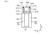
本実施形態は、図9に示すごとく、一対の共存配置部41P、41Nのうちの一方について、接続部よりもモジュール本体部20から遠い位置に突出対向部44zを配置した形態である。 Second Embodiment
In the present embodiment, as shown in FIG. 9, theprotrusion facing portion 44z is disposed at a position farther from the module main body 20 than the connection portion for one of the pair of coexistence / arrangement portions 41P and 41N.
本実施形態は、図9に示すごとく、一対の共存配置部41P、41Nのうちの一方について、接続部よりもモジュール本体部20から遠い位置に突出対向部44zを配置した形態である。 Second Embodiment
In the present embodiment, as shown in FIG. 9, the
本実施形態においては、負極バスバー4Nの共存配置部41Nについて、接続部11Nよりもモジュール本体部20から遠い位置に突出対向部44zを配置している。そして、負極バスバー4Nの突出対向部44zは、負極端子21Nの先端よりも、モジュール本体部20から遠い位置に配されている。
共存配置部41Nは、並び対向部44xを、突出対向部44zよりもモジュール本体部20に近い側に配置している。 In the present embodiment, in thecoexistence arrangement portion 41N of the negative electrode bus bar 4N, the protruding facing portion 44z is arranged at a position farther from the module main body portion 20 than the connection portion 11N. The protruding opposing portion 44z of the negative electrode bus bar 4N is disposed at a position farther from the module body 20 than the tip of the negative electrode terminal 21N.
Thecoexistence arrangement portion 41N arranges the row facing portion 44x closer to the module body portion 20 than the protruding facing portion 44z.
共存配置部41Nは、並び対向部44xを、突出対向部44zよりもモジュール本体部20に近い側に配置している。 In the present embodiment, in the
The
なお、正極バスバー4Pの共存配置部41Pについては、接続部11Pよりも突出対向部44zを、モジュール本体部20に近い側に配置している。すなわち、一対の共存配置部41P、41Nのうち、突出対向部44zが、モジュール本体部20に近い側に配された共存配置部41Pは、突出対向部44zを、接続部11Pよりもモジュール本体部20に近い位置に配置している。この点は、実施形態1と同様である。
In the coexistence arrangement portion 41P of the positive electrode bus bar 4P, the protrusion facing portion 44z is arranged closer to the module body 20 than the connection portion 11P. That is, the coexistence arrangement portion 41P, in which the protrusion facing portion 44z is disposed closer to the module body portion 20, of the pair of coexistence arrangement portions 41P and 41N, is closer to the module body portion than the connection portion 11P. It is placed near 20. This point is the same as that of the first embodiment.
その他の構成についても、実施形態1と同様である。
なお、実施形態2以降において用いた符号のうち、既出の実施形態において用いた符号と同一のものは、特に示さない限り、既出の実施形態におけるものと同様の構成要素等を表す。 The other configuration is the same as that of the first embodiment.
In addition, the code | symbol same as the code | symbol used in already-appeared embodiment among the code | symbol used inEmbodiment 2 or subsequent ones represents the component similar to the thing in already-appeared embodiment, etc., unless shown.
なお、実施形態2以降において用いた符号のうち、既出の実施形態において用いた符号と同一のものは、特に示さない限り、既出の実施形態におけるものと同様の構成要素等を表す。 The other configuration is the same as that of the first embodiment.
In addition, the code | symbol same as the code | symbol used in already-appeared embodiment among the code | symbol used in
本実施形態においても、一対の共存配置部41P、41Nが、それぞれの一部を、一対のパワー端子21の間に配置している。これにより、インダクタンスを低減することができる。また、一対の上記共存配置部41P、41Nは、並び対向部44xと突出対向部44zとを有する。これにより、インダクタンスを効果的に低減することができる。
Also in the present embodiment, the pair of coexistence / arrangement portions 41P and 41N arrange a part of each between the pair of power terminals 21. This can reduce the inductance. Further, the pair of coexistence / arrangement portions 41P and 41N have a row opposing portion 44x and a projecting opposing portion 44z. Thereby, the inductance can be effectively reduced.
また、突出対向部44zがモジュール本体部20に近い側に配された共存配置部41Pについては、突出対向部44zを接続部11Pよりもモジュール本体部20に近い位置に配置している。これにより、モジュール本体部20の内部におけるスイッチング素子及び内部配線と、共存配置部41Pと、パワー端子21とによって形成される電流ループを小さくすることができる。その結果、インダクタンスを低減することができる。
その他、実施形態1と同様の作用効果を有する。 Further, in thecoexistence arrangement portion 41P in which the projecting facing portion 44z is disposed closer to the module body portion 20, the projecting facing portion 44z is disposed at a position closer to the module body portion 20 than the connecting portion 11P. As a result, the current loop formed by the switching element and the internal wiring inside the module main body portion 20, the coexistence placement portion 41P, and the power terminal 21 can be reduced. As a result, the inductance can be reduced.
In addition, it has the same operation effect asEmbodiment 1.
その他、実施形態1と同様の作用効果を有する。 Further, in the
In addition, it has the same operation effect as
(実施形態3)
本実施形態においては、図10に示すごとく、一対の共存配置部41P、41Nの双方について、接続部11P、11Nよりもモジュール本体部20から遠い位置に突出対向部44zを配置した形態である。 (Embodiment 3)
In the present embodiment, as shown in FIG. 10, the projecting opposingportion 44z is disposed at a position farther from the module main body 20 than the connecting portions 11P and 11N for both of the pair of coexistence / arrangement portions 41P and 41N.
本実施形態においては、図10に示すごとく、一対の共存配置部41P、41Nの双方について、接続部11P、11Nよりもモジュール本体部20から遠い位置に突出対向部44zを配置した形態である。 (Embodiment 3)
In the present embodiment, as shown in FIG. 10, the projecting opposing
また、突出対向部44zは、並び対向部44xよりもモジュール本体部20から遠い側に配置している。また、一対の突出対向部44zは、パワー端子21の先端よりも、モジュール本体部20から遠い位置に配されている。
そして、一対の突出対向部44zは、Z方向において、近接して対向配置されている。
その他の構成は、実施形態1と同様である。 Further, the protruding facingportion 44z is disposed farther from the module main body portion 20 than the line facing portion 44x. Further, the pair of projecting facing portions 44 z is disposed at a position farther from the module body 20 than the tip of the power terminal 21.
And a pair of projecting opposingparts 44z adjoin and are opposingly arranged in the Z direction.
The other configuration is the same as that of the first embodiment.
そして、一対の突出対向部44zは、Z方向において、近接して対向配置されている。
その他の構成は、実施形態1と同様である。 Further, the protruding facing
And a pair of projecting opposing
The other configuration is the same as that of the first embodiment.
本実施形態においても、一対の共存配置部41P、41Nが、それぞれの一部を、一対のパワー端子21の間に配置している。これにより、インダクタンスを低減することができる。また、一対の上記共存配置部41P、41Nは、並び対向部44xと突出対向部44zとを有する。これにより、インダクタンスを効果的に低減することができる。
Also in the present embodiment, the pair of coexistence / arrangement portions 41P and 41N arrange a part of each between the pair of power terminals 21. This can reduce the inductance. Further, the pair of coexistence / arrangement portions 41P and 41N have a row opposing portion 44x and a projecting opposing portion 44z. Thereby, the inductance can be effectively reduced.
また、本実施形態においては、特に、一対の共存配置部41P、41Nのうち、突出対向部44zがモジュール本体部20により近い側に配された、共存配置部41Pが、突出対向部44zを、接続部11Pよりもモジュール本体部20から遠い位置に配置している。これにより、突出対向部44zと冷却管31との間の距離を確保して、両者の絶縁を確保しやすい。
その他、実施形態1と同様の作用効果を有する。 Further, in the present embodiment, thecoexistence arrangement portion 41P, of the pair of coexistence arrangement portions 41P and 41N, in which the protrusion facing portion 44z is disposed closer to the module body portion 20, corresponds to the protrusion facing portion 44z, It arrange | positions in the position far from the module main-body part 20 rather than the connection part 11P. As a result, the distance between the protrusion facing portion 44z and the cooling pipe 31 can be secured, and the insulation between the two can be easily secured.
In addition, it has the same operation effect asEmbodiment 1.
その他、実施形態1と同様の作用効果を有する。 Further, in the present embodiment, the
In addition, it has the same operation effect as
(実施形態4)
本実施形態は、図11に示すごとく、共存配置部41Pにおける正極バスバー4Pと正極端子21Pとの接続部11Pと、共存配置部41Nにおける負極バスバー4Nと負極端子21Nとの接続部11Nとは、Z方向における位置が互いに異なる形態である。 (Embodiment 4)
In the present embodiment, as shown in FIG. 11, theconnection portion 11P of the positive electrode bus bar 4P and the positive electrode terminal 21P in the coexistence arrangement portion 41P and the connection portion 11N of the negative electrode busbar 4N and the negative electrode terminal 21N in the coexistence arrangement portion 41N are The positions in the Z direction are different from each other.
本実施形態は、図11に示すごとく、共存配置部41Pにおける正極バスバー4Pと正極端子21Pとの接続部11Pと、共存配置部41Nにおける負極バスバー4Nと負極端子21Nとの接続部11Nとは、Z方向における位置が互いに異なる形態である。 (Embodiment 4)
In the present embodiment, as shown in FIG. 11, the
特に、突出対向部44zがよりモジュール本体部20側に配された共存配置部41Pが、その接続部11Pを、他方の共存配置部41Nよりも、モジュール本体部20に近い側に配している。正極端子21Pにおけるモジュール本体部20から接続部11Pまでの電流経路を極力短くすることができる。その結果、インダクタンスを低減することができる。
In particular, the coexistence arrangement portion 41P in which the protruding facing portion 44z is disposed closer to the module main body 20 side has the connection portion 11P disposed closer to the module main body portion 20 than the other coexistence arrangement portion 41N. . The current path from the module main body 20 to the connection portion 11P in the positive electrode terminal 21P can be shortened as much as possible. As a result, the inductance can be reduced.
すなわち、接続性等の観点からは、並び対向部44xのZ方向の長さをある程度確保することが望ましい。突出対向部44zがモジュール本体部20に近い側に配された正極側の共存配置部41Pは、モジュール本体部20に比較的近い位置に並び対向部44xの先端を設けても、接続性を確保することができる。そこで、なるべく、モジュール本体部20に近い位置に、正極側の接続部11Pを設けている。一方、負極側の接続部11Nは、ある程度モジュール本体部20から遠い位置にしないと、並び対向部44xのZ方向の長さを確保しにくい。それゆえ、極力、正極側の接続部11Pをモジュール本体部20に近付けると、結果的に、負極側の接続部11Nよりも、モジュール本体部20に近くなる。
その他の構成は、実施形態1と同様である。 That is, from the viewpoint of connectivity and the like, it is desirable to secure the length in the Z direction of therow facing portion 44x to a certain extent. The coexistence placement portion 41P on the positive electrode side, in which the protruding facing portion 44z is disposed closer to the module body portion 20, ensures connectivity even when the leading end of the facing portion 44x is arranged relatively close to the module body portion 20. can do. Therefore, the connection portion 11P on the positive electrode side is provided as close to the module body 20 as possible. On the other hand, unless the connecting portion 11N on the negative electrode side is at a position far from the module main body 20 to some extent, it is difficult to secure the length in the Z direction of the facing portion 44x. Therefore, when the connection portion 11P on the positive electrode side is brought close to the module body 20 as much as possible, as a result, it becomes closer to the module body 20 than the connection portion 11N on the negative electrode side.
The other configuration is the same as that of the first embodiment.
その他の構成は、実施形態1と同様である。 That is, from the viewpoint of connectivity and the like, it is desirable to secure the length in the Z direction of the
The other configuration is the same as that of the first embodiment.
本実施形態においては、上述のように、インダクタンスをより低減することができる。その他、実施形態1と同様の作用効果を有する。
In the present embodiment, as described above, the inductance can be further reduced. In addition, it has the same operation effect as Embodiment 1.
(実施形態5)
本実施形態は、図12に示すごとく、第1半導体モジュール2P及び第2半導体モジュール2Nが、互いに並列接続された複数のスイッチング素子を内蔵してなる形態である。
すなわち、第1半導体モジュール2Pは、互いに並列接続された複数の上アームスイッチング素子20uを内蔵している。また、第2半導体モジュール2Nは、互いに並列接続された複数の下アームスイッチング素子20dを内蔵している。
その他の構成は、実施形態1と同様である。 Embodiment 5
In this embodiment, as shown in FIG. 12, thefirst semiconductor module 2P and the second semiconductor module 2N incorporate a plurality of switching elements connected in parallel to each other.
That is, thefirst semiconductor module 2P incorporates a plurality of upper arm switching elements 20u connected in parallel to each other. Further, the second semiconductor module 2N incorporates a plurality of lower arm switching elements 20d connected in parallel to each other.
The other configuration is the same as that of the first embodiment.
本実施形態は、図12に示すごとく、第1半導体モジュール2P及び第2半導体モジュール2Nが、互いに並列接続された複数のスイッチング素子を内蔵してなる形態である。
すなわち、第1半導体モジュール2Pは、互いに並列接続された複数の上アームスイッチング素子20uを内蔵している。また、第2半導体モジュール2Nは、互いに並列接続された複数の下アームスイッチング素子20dを内蔵している。
その他の構成は、実施形態1と同様である。 Embodiment 5
In this embodiment, as shown in FIG. 12, the
That is, the
The other configuration is the same as that of the first embodiment.
本実施形態においては、各アームに流れる電流の許容値を大きくすることができる。それゆえ、より高出力の電力変換装置1を得ることができる。
その他、実施形態1と同様の作用効果を有する。 In the present embodiment, the allowable value of the current flowing to each arm can be increased. Therefore, thepower converter 1 with higher output can be obtained.
In addition, it has the same operation effect asEmbodiment 1.
その他、実施形態1と同様の作用効果を有する。 In the present embodiment, the allowable value of the current flowing to each arm can be increased. Therefore, the
In addition, it has the same operation effect as
本実施形態においては、各半導体モジュール2が、互いに並列接続された2個のスイッチング素子を内蔵した例を示したが、半導体モジュール2としては、互いに並列接続された3個以上のスイッチング素子を内蔵したものとすることもできる。また、互いに並列接続するスイッチング素子としては、同種のものを並列接続してもよいし、異種のスイッチング素子を並列接続して内蔵してもよい。
In the present embodiment, an example is shown in which each semiconductor module 2 incorporates two switching elements connected in parallel with each other. However, as the semiconductor module 2, three or more switching elements connected in parallel with each other are incorporated. It can also be done. Further, as the switching elements connected in parallel with each other, the same kind of elements may be connected in parallel, or different switching elements may be connected in parallel and incorporated.
例えば、一つの半導体モジュール2に、SiC-MOSFETとSi-IGBTとを並列接続してもよい。SiC-MOSFETは、SiC(すなわち、炭化シリコン)によって形成されるMOSFETである。また、Si-IGBTは、Si(すなわち、シリコン)によって形成されるIGBTである。
For example, a SiC-MOSFET and a Si-IGBT may be connected in parallel to one semiconductor module 2. The SiC-MOSFET is a MOSFET formed of SiC (ie, silicon carbide). The Si-IGBT is an IGBT formed of Si (ie, silicon).
なお、第1半導体モジュール2P及び第2半導体モジュール2Nの少なくとも一つが、互いに並列接続された複数のスイッチング素子を内蔵するようにしてもよい。
また、上述の実施形態においては、正極バスバーの共存配置部を、負極バスバーの共存配置部よりも、モジュール本体部に近い側に配した形態を示したが、この位置関係は特に限定されるものではない。すなわち、負極バスバーの共存配置部を、正極バスバーの共存配置部よりも、モジュール本体部に近い側に配した形態とすることもできる。また、一対の共存配置部を、モジュール本体部からの距離が同じになるように配してもよい。 Note that at least one of thefirst semiconductor module 2P and the second semiconductor module 2N may incorporate a plurality of switching elements connected in parallel with each other.
In the above embodiment, the coexistence arrangement portion of the positive electrode bus bar is disposed closer to the module main portion than the coexistence arrangement portion of the negative electrode bus bar, but this positional relationship is particularly limited. is not. That is, the coexistence arrangement portion of the negative electrode bus bar may be disposed closer to the module main body than the coexistence arrangement portion of the positive electrode bus bar. In addition, the pair of coexistence placement units may be disposed so as to have the same distance from the module main body.
また、上述の実施形態においては、正極バスバーの共存配置部を、負極バスバーの共存配置部よりも、モジュール本体部に近い側に配した形態を示したが、この位置関係は特に限定されるものではない。すなわち、負極バスバーの共存配置部を、正極バスバーの共存配置部よりも、モジュール本体部に近い側に配した形態とすることもできる。また、一対の共存配置部を、モジュール本体部からの距離が同じになるように配してもよい。 Note that at least one of the
In the above embodiment, the coexistence arrangement portion of the positive electrode bus bar is disposed closer to the module main portion than the coexistence arrangement portion of the negative electrode bus bar, but this positional relationship is particularly limited. is not. That is, the coexistence arrangement portion of the negative electrode bus bar may be disposed closer to the module main body than the coexistence arrangement portion of the positive electrode bus bar. In addition, the pair of coexistence placement units may be disposed so as to have the same distance from the module main body.
本開示は上記各実施形態に限定されるものではなく、その要旨を逸脱しない範囲において種々の実施形態に適用することが可能である。
The present disclosure is not limited to the above embodiments, and can be applied to various embodiments without departing from the scope of the invention.
本開示は、実施形態に準拠して記述されたが、本開示は当該実施形態や構造に限定されるものではないと理解される。本開示は、様々な変形例や均等範囲内の変形をも包含する。加えて、様々な組み合わせや形態、さらには、それらに一要素のみ、それ以上、あるいはそれ以下、を含む他の組み合わせや形態をも、本開示の範疇や思想範囲に入るものである。
Although the present disclosure has been described in accordance with the embodiment, it is understood that the present disclosure is not limited to the embodiment or the structure. The present disclosure also includes various modifications and variations within the equivalent range. In addition, various combinations and forms, and further, other combinations and forms including only one element, or more or less than these elements are also within the scope and the scope of the present disclosure.
Claims (16)
- 正極配線に接続される複数の上アームスイッチング素子(20u)と、負極配線に接続される複数の下アームスイッチング素子(20d)とを有するスイッチング回路部(101)を備えた電力変換装置(1)であって、
複数のバスバー(4)と、
モジュール本体部(20)からパワー端子(21)を突出してなる複数の半導体モジュール(2)と、を有し、
上記バスバーとして、上記正極配線を構成する正極バスバー(4P)と、上記負極配線を構成する負極バスバー(4N)と、を有し、
上記半導体モジュールとして、上記上アームスイッチング素子を内蔵すると共に上記正極バスバーに接続される上記パワー端子である正極端子(21P)を備えた第1半導体モジュール(2P)と、上記下アームスイッチング素子を内蔵すると共に上記負極バスバーに接続される上記パワー端子である負極端子(21N)を備えた第2半導体モジュール(2N)と、を有し、
上記第1半導体モジュールと上記第2半導体モジュールとは、上記正極端子と上記負極端子とを突出方向に直交する方向に対向させた状態で、配置されており、
上記正極バスバー及び上記負極バスバーは、上記パワー端子の突出方向から見たとき、共に上記正極端子と上記負極端子との間に配される共存配置部(41P、41N)をそれぞれ有し、
上記共存配置部の少なくとも一部は、上記正極端子と上記負極端子との間の空間に配されている、電力変換装置。 Power converter (1) comprising a switching circuit unit (101) having a plurality of upper arm switching elements (20u) connected to a positive electrode wiring and a plurality of lower arm switching elements (20d) connected to a negative electrode wiring And
With multiple bus bars (4),
A plurality of semiconductor modules (2) formed by projecting a power terminal (21) from a module body (20);
As the bus bar, a positive bus bar (4P) constituting the positive wiring, and a negative bus bar (4N) constituting the negative wiring,
As the semiconductor module, a first semiconductor module (2P) including the positive arm terminal (21P) which is the power terminal connected to the positive bus bar and has the built-in upper arm switching element and the lower arm switching element. And a second semiconductor module (2N) having a negative terminal (21N) which is the power terminal connected to the negative bus bar.
The first semiconductor module and the second semiconductor module are disposed in a state in which the positive electrode terminal and the negative electrode terminal are opposed to each other in a direction orthogonal to the protruding direction,
The positive electrode bus bar and the negative electrode bus bar both have coexistence placement portions (41P, 41N) disposed between the positive electrode terminal and the negative electrode terminal, respectively, when viewed from the projecting direction of the power terminal,
At least one part of the said coexistence arrangement | positioning part is a power converter device distribute | arranged to the space between the said positive electrode terminal and the said negative electrode terminal. - 上記共存配置部は、互いの主面が対向するように配置された対向部(44x、44z)を有する、請求項1に記載の電力変換装置。 The power conversion device according to claim 1, wherein the coexistence arrangement part has opposing parts (44x, 44z) arranged such that the main surfaces of the coexistence arrangement parts face each other.
- 上記共存配置部は、上記対向部として、上記正極端子と上記負極端子との並び方向に対向する並び対向部(44x)を有する、請求項2に記載の電力変換装置。 The power conversion device according to claim 2, wherein the coexistence arrangement portion has, as the facing portion, a row facing portion (44x) facing in the direction in which the positive electrode terminal and the negative electrode terminal are aligned.
- 上記共存配置部は、上記対向部として、上記パワー端子の突出方向に対向する突出対向部(44z)を有する、請求項2又は3に記載の電力変換装置。 The power conversion device according to claim 2 or 3, wherein the coexistence arrangement portion has a protruding facing portion (44z) facing in the protruding direction of the power terminal as the facing portion.
- 上記共存配置部は、上記対向部として、上記正極端子と上記負極端子との並び方向に対向する並び対向部(44x)と、上記突出対向部とを有する、請求項4に記載の電力変換装置。 The power conversion device according to claim 4, wherein the coexistence arrangement portion has, as the facing portion, a row facing portion (44x) facing in the direction in which the positive electrode terminal and the negative electrode terminal are aligned, and the protruding facing portion. .
- 上記突出対向部における一対の上記共存配置部の間の間隔d1は、上記並び対向部における一対の上記共存配置部の間の間隔d2よりも小さい、請求項5に記載の電力変換装置。 The power conversion device according to claim 5, wherein a distance d1 between the pair of coexistence / arrangement portions in the protrusion facing portion is smaller than a distance d2 between the pair of coexistence / arrangement portions in the row facing portion.
- 上記正極端子と上記負極端子との並び方向における上記突出対向部の長さL1は、上記パワー端子の突出方向における上記並び対向部の長さL2よりも長い、請求項5又は6に記載の電力変換装置。 The power according to claim 5 or 6, wherein a length L1 of the protruding facing portion in the direction in which the positive electrode terminal and the negative electrode terminal are lined is longer than a length L2 of the row facing portion in the protruding direction of the power terminal. Converter.
- 一対の上記共存配置部のうち、上記突出対向部が、上記モジュール本体部に近い側に配された上記共存配置部は、上記突出対向部を、上記パワー端子との接続部よりも上記モジュール本体部に近い位置に配置している、請求項4~7のいずれか一項に記載の電力変換装置。 Among the pair of coexistence and arrangement parts, the coexistence arrangement part in which the protrusion opposing part is disposed closer to the module body part is the module body than the connection part with the power terminal. The power conversion device according to any one of claims 4 to 7, wherein the power conversion device is arranged at a position close to the unit.
- 一対の上記共存配置部のうち、上記突出対向部が上記モジュール本体部により近い側に配された上記共存配置部は、上記突出対向部を、上記パワー端子との接続部よりも上記モジュール本体部から遠い位置に配置している、請求項4~7のいずれか一項に記載の電力変換装置。 Among the pair of coexistence arrangement parts, the coexistence arrangement part in which the protrusion opposing part is disposed closer to the module body part is the module body part than the connection part with the power terminal. The power conversion device according to any one of claims 4 to 7, wherein the power conversion device is disposed at a position distant from the
- 上記第1半導体モジュール及び上記第2半導体モジュールの少なくとも一つは、互いに並列接続された複数のスイッチング素子を内蔵してなる、請求項1~9のいずれか一項に記載の電力変換装置。 The power conversion device according to any one of claims 1 to 9, wherein at least one of the first semiconductor module and the second semiconductor module includes a plurality of switching elements connected in parallel to each other.
- 互いに隣り合う位置に配置された上記第1半導体モジュールと上記第2半導体モジュールとの間には、冷媒流路を内部に有する冷却管(3)が介在している、請求項1~10のいずれか一項に記載の電力変換装置。 11. A cooling pipe (3) having a refrigerant flow path inside is interposed between the first semiconductor module and the second semiconductor module arranged at mutually adjacent positions. The power converter according to any one of the preceding claims.
- 上記共存配置部における上記正極バスバーと上記正極端子との接続部(11P)と、上記共存配置部における上記負極バスバーと上記負極端子との接続部(11N)とは、上記パワー端子の突出方向における位置が同等である、請求項1~11のいずれか一項に記載の電力変換装置。 The connection portion (11P) between the positive electrode bus bar and the positive electrode terminal in the coexistence arrangement portion and the connection portion (11N) between the negative electrode bus bar and the negative electrode terminal in the coexistence arrangement portion are in the protrusion direction of the power terminal The power converter according to any one of claims 1 to 11, wherein the positions are equal.
- 上記共存配置部における上記正極バスバーと上記正極端子との接続部と、上記共存配置部における上記負極バスバーと上記負極端子との接続部とは、上記パワー端子の突出方向における位置が互いに異なる、請求項1~11のいずれか一項に記載の電力変換装置。 The connection portion between the positive electrode bus bar and the positive electrode terminal in the coexistence arrangement portion and the connection portion between the negative electrode bus bar and the negative electrode terminal in the coexistence arrangement portion have different positions in the projecting direction of the power terminal. Item 12. The power conversion device according to any one of items 1 to 11.
- 出力配線を構成する出力バスバー(4O)を有し、上記半導体モジュールは、上記パワー端子の一つとして、上記出力バスバーに接続される出力端子(21O)を有し、上記第1半導体モジュールと上記第2半導体モジュールとは、互いの上記出力端子同士を対向配置させてなり、上記出力バスバーは、対向配置された上記出力端子同士の間の空間に配される出力介在部(41O)を有し、該出力介在部に、上記第1半導体モジュールの上記出力端子と上記第2半導体モジュールの上記出力端子との双方が接続されている、請求項1~13のいずれか一項に記載の電力変換装置。 The semiconductor module includes an output bus bar (4O) constituting an output wiring, and the semiconductor module has an output terminal (21O) connected to the output bus bar as one of the power terminals, and the first semiconductor module and the above In the second semiconductor module, the output terminals are arranged opposite to each other, and the output bus bar has an output interposed portion (41O) disposed in the space between the output terminals arranged opposite to each other. The power conversion according to any one of claims 1 to 13, wherein both the output terminal of the first semiconductor module and the output terminal of the second semiconductor module are connected to the output intervening portion. apparatus.
- 隣り合う上記第1半導体モジュールと上記第2半導体モジュールとの間に配された、上記出力介在部と上記共存配置部とは、それぞれの上記パワー端子との接続部(11P、11N、11O)を、上記パワー端子の突出方向における同等の位置に有する、請求項14に記載の電力変換装置。 The output intervening portion and the coexistence / arrangement portion disposed between the adjacent first semiconductor module and the second semiconductor module are connected portions (11P, 11N, 11O) with the respective power terminals. The power converter according to claim 14, wherein the power converter has the same position in the projecting direction of the power terminal.
- 上記出力介在部は、上記パワー端子の突出方向を向く主面を有する基板部(451)と、該基板部から上記パワー端子の突出方向に立ち上がる一対の立設部(452)とを有し、上記基板部は、上記パワー端子の突出方向において、上記出力端子の先端との距離よりも上記モジュール本体部との距離の方が短い、請求項14又は15に記載の電力変換装置。 The output interposed portion has a substrate portion (451) having a main surface facing the protrusion direction of the power terminal, and a pair of standing portions (452) rising from the substrate portion in the protrusion direction of the power terminal. The power conversion device according to claim 14, wherein a distance between the substrate and the module main body is shorter than a distance between the substrate and the end of the output terminal in the protruding direction of the power terminal.
Priority Applications (1)
| Application Number | Priority Date | Filing Date | Title |
|---|---|---|---|
| US16/782,158 US11509234B2 (en) | 2017-08-09 | 2020-02-05 | Power conversion apparatus |
Applications Claiming Priority (2)
| Application Number | Priority Date | Filing Date | Title |
|---|---|---|---|
| JP2017-154398 | 2017-08-09 | ||
| JP2017154398A JP2019033628A (en) | 2017-08-09 | 2017-08-09 | Power conversion device |
Related Child Applications (1)
| Application Number | Title | Priority Date | Filing Date |
|---|---|---|---|
| US16/782,158 Continuation US11509234B2 (en) | 2017-08-09 | 2020-02-05 | Power conversion apparatus |
Publications (1)
| Publication Number | Publication Date |
|---|---|
| WO2019031211A1 true WO2019031211A1 (en) | 2019-02-14 |
Family
ID=65272174
Family Applications (1)
| Application Number | Title | Priority Date | Filing Date |
|---|---|---|---|
| PCT/JP2018/027482 WO2019031211A1 (en) | 2017-08-09 | 2018-07-23 | Power conversion device |
Country Status (3)
| Country | Link |
|---|---|
| US (1) | US11509234B2 (en) |
| JP (2) | JP2019033628A (en) |
| WO (1) | WO2019031211A1 (en) |
Cited By (1)
| Publication number | Priority date | Publication date | Assignee | Title |
|---|---|---|---|---|
| JP2020145321A (en) * | 2019-03-06 | 2020-09-10 | 株式会社デンソー | Semiconductor module |
Families Citing this family (1)
| Publication number | Priority date | Publication date | Assignee | Title |
|---|---|---|---|---|
| JP7052783B2 (en) * | 2019-08-27 | 2022-04-12 | 株式会社デンソー | Energized part for power conversion circuit |
Citations (5)
| Publication number | Priority date | Publication date | Assignee | Title |
|---|---|---|---|---|
| JP2008253055A (en) * | 2007-03-30 | 2008-10-16 | Denso Corp | Power converter |
| JP2015015787A (en) * | 2013-07-03 | 2015-01-22 | 株式会社デンソー | Power conversion device |
| JP2015136224A (en) * | 2014-01-16 | 2015-07-27 | トヨタ自動車株式会社 | power converter |
| JP2015149883A (en) * | 2014-01-09 | 2015-08-20 | 株式会社デンソー | Power conversion device |
| JP2016163396A (en) * | 2015-02-27 | 2016-09-05 | トヨタ自動車株式会社 | Power conversion device |
Family Cites Families (6)
| Publication number | Priority date | Publication date | Assignee | Title |
|---|---|---|---|---|
| US7042086B2 (en) * | 2002-10-16 | 2006-05-09 | Nissan Motor Co., Ltd. | Stacked semiconductor module and assembling method of the same |
| JP5380376B2 (en) * | 2010-06-21 | 2014-01-08 | 日立オートモティブシステムズ株式会社 | Power semiconductor device |
| JP5488638B2 (en) * | 2012-04-11 | 2014-05-14 | 株式会社デンソー | Power converter |
| CN104412383B (en) * | 2012-06-29 | 2017-09-26 | 株式会社电装 | The connecting structure of semiconductor device and semiconductor device |
| JP2015149833A (en) * | 2014-02-06 | 2015-08-20 | デクセリアルズ株式会社 | Electronic apparatus |
| CN105580503B (en) * | 2014-03-27 | 2019-03-01 | 株式会社日立制作所 | The manufacturing method of electric power conversion unit, power-converting device and power-converting device |
-
2017
- 2017-08-09 JP JP2017154398A patent/JP2019033628A/en active Pending
-
2018
- 2018-07-23 WO PCT/JP2018/027482 patent/WO2019031211A1/en active Application Filing
-
2020
- 2020-02-05 US US16/782,158 patent/US11509234B2/en active Active
-
2021
- 2021-09-09 JP JP2021146881A patent/JP7375797B2/en active Active
Patent Citations (5)
| Publication number | Priority date | Publication date | Assignee | Title |
|---|---|---|---|---|
| JP2008253055A (en) * | 2007-03-30 | 2008-10-16 | Denso Corp | Power converter |
| JP2015015787A (en) * | 2013-07-03 | 2015-01-22 | 株式会社デンソー | Power conversion device |
| JP2015149883A (en) * | 2014-01-09 | 2015-08-20 | 株式会社デンソー | Power conversion device |
| JP2015136224A (en) * | 2014-01-16 | 2015-07-27 | トヨタ自動車株式会社 | power converter |
| JP2016163396A (en) * | 2015-02-27 | 2016-09-05 | トヨタ自動車株式会社 | Power conversion device |
Cited By (2)
| Publication number | Priority date | Publication date | Assignee | Title |
|---|---|---|---|---|
| JP2020145321A (en) * | 2019-03-06 | 2020-09-10 | 株式会社デンソー | Semiconductor module |
| JP7124769B2 (en) | 2019-03-06 | 2022-08-24 | 株式会社デンソー | semiconductor module |
Also Published As
| Publication number | Publication date |
|---|---|
| JP2019033628A (en) | 2019-02-28 |
| JP2021185742A (en) | 2021-12-09 |
| US20200177093A1 (en) | 2020-06-04 |
| US11509234B2 (en) | 2022-11-22 |
| JP7375797B2 (en) | 2023-11-08 |
Similar Documents
| Publication | Publication Date | Title |
|---|---|---|
| JP6272385B2 (en) | Semiconductor device | |
| US11538794B2 (en) | Power converter with an upper arm and a lower arm and at least first and second semiconductor devices connected by a bridging member | |
| US9184670B2 (en) | Power conversion device | |
| JP6086863B2 (en) | Semiconductor module | |
| JP5924164B2 (en) | Semiconductor device | |
| US7869193B2 (en) | Power conversion apparatus | |
| JP6753475B2 (en) | Semiconductor modules, electric vehicles, and power control units | |
| JP2019118164A (en) | Power conversion system | |
| JP5893369B2 (en) | Semiconductor device | |
| JP2019030043A (en) | Power conversion device | |
| US20110284924A1 (en) | Semiconductor device, semiconductor unit, and power semiconductor device | |
| JP7375797B2 (en) | power converter | |
| JP2012034566A (en) | Bus bar module | |
| US20130242631A1 (en) | Power converter apparatus | |
| JP6647189B2 (en) | Semiconductor module, semiconductor device and power device | |
| JP2013099213A (en) | Inverter device | |
| CN113728546A (en) | Power conversion device | |
| WO2019031546A1 (en) | Electric power conversion device | |
| JP6583137B2 (en) | Power converter | |
| CN111668165B (en) | Semiconductor module and semiconductor device provided with same | |
| JP6123722B2 (en) | Semiconductor device | |
| JP7003641B2 (en) | Semiconductor modules and power converters | |
| JP2012222133A (en) | Semiconductor module and power converter using the same | |
| JP2019161997A (en) | Power conversion equipment | |
| JP2020089034A (en) | Switching element unit |
Legal Events
| Date | Code | Title | Description |
|---|---|---|---|
| 121 | Ep: the epo has been informed by wipo that ep was designated in this application |
Ref document number: 18843209 Country of ref document: EP Kind code of ref document: A1 |
|
| NENP | Non-entry into the national phase |
Ref country code: DE |
|
| 122 | Ep: pct application non-entry in european phase |
Ref document number: 18843209 Country of ref document: EP Kind code of ref document: A1 |