WO2019019278A1 - 阵列基板及其制作方法 - Google Patents
阵列基板及其制作方法 Download PDFInfo
- Publication number
- WO2019019278A1 WO2019019278A1 PCT/CN2017/100718 CN2017100718W WO2019019278A1 WO 2019019278 A1 WO2019019278 A1 WO 2019019278A1 CN 2017100718 W CN2017100718 W CN 2017100718W WO 2019019278 A1 WO2019019278 A1 WO 2019019278A1
- Authority
- WO
- WIPO (PCT)
- Prior art keywords
- via hole
- layer
- insulating layer
- hole
- array substrate
- Prior art date
- Legal status (The legal status is an assumption and is not a legal conclusion. Google has not performed a legal analysis and makes no representation as to the accuracy of the status listed.)
- Ceased
Links
Images


Classifications
-
- H—ELECTRICITY
- H10—SEMICONDUCTOR DEVICES; ELECTRIC SOLID-STATE DEVICES NOT OTHERWISE PROVIDED FOR
- H10D—INORGANIC ELECTRIC SEMICONDUCTOR DEVICES
- H10D86/00—Integrated devices formed in or on insulating or conducting substrates, e.g. formed in silicon-on-insulator [SOI] substrates or on stainless steel or glass substrates
- H10D86/40—Integrated devices formed in or on insulating or conducting substrates, e.g. formed in silicon-on-insulator [SOI] substrates or on stainless steel or glass substrates characterised by multiple TFTs
-
- H—ELECTRICITY
- H10—SEMICONDUCTOR DEVICES; ELECTRIC SOLID-STATE DEVICES NOT OTHERWISE PROVIDED FOR
- H10D—INORGANIC ELECTRIC SEMICONDUCTOR DEVICES
- H10D30/00—Field-effect transistors [FET]
- H10D30/01—Manufacture or treatment
- H10D30/021—Manufacture or treatment of FETs having insulated gates [IGFET]
- H10D30/031—Manufacture or treatment of FETs having insulated gates [IGFET] of thin-film transistors [TFT]
- H10D30/0312—Manufacture or treatment of FETs having insulated gates [IGFET] of thin-film transistors [TFT] characterised by the gate electrodes
- H10D30/0314—Manufacture or treatment of FETs having insulated gates [IGFET] of thin-film transistors [TFT] characterised by the gate electrodes of lateral top-gate TFTs comprising only a single gate
-
- H—ELECTRICITY
- H10—SEMICONDUCTOR DEVICES; ELECTRIC SOLID-STATE DEVICES NOT OTHERWISE PROVIDED FOR
- H10D—INORGANIC ELECTRIC SEMICONDUCTOR DEVICES
- H10D30/00—Field-effect transistors [FET]
- H10D30/01—Manufacture or treatment
- H10D30/021—Manufacture or treatment of FETs having insulated gates [IGFET]
- H10D30/031—Manufacture or treatment of FETs having insulated gates [IGFET] of thin-film transistors [TFT]
- H10D30/0321—Manufacture or treatment of FETs having insulated gates [IGFET] of thin-film transistors [TFT] comprising silicon, e.g. amorphous silicon or polysilicon
-
- H—ELECTRICITY
- H10—SEMICONDUCTOR DEVICES; ELECTRIC SOLID-STATE DEVICES NOT OTHERWISE PROVIDED FOR
- H10D—INORGANIC ELECTRIC SEMICONDUCTOR DEVICES
- H10D30/00—Field-effect transistors [FET]
- H10D30/60—Insulated-gate field-effect transistors [IGFET]
- H10D30/67—Thin-film transistors [TFT]
- H10D30/6729—Thin-film transistors [TFT] characterised by the electrodes
- H10D30/673—Thin-film transistors [TFT] characterised by the electrodes characterised by the shapes, relative sizes or dispositions of the gate electrodes
- H10D30/6731—Top-gate only TFTs
-
- H—ELECTRICITY
- H10—SEMICONDUCTOR DEVICES; ELECTRIC SOLID-STATE DEVICES NOT OTHERWISE PROVIDED FOR
- H10D—INORGANIC ELECTRIC SEMICONDUCTOR DEVICES
- H10D30/00—Field-effect transistors [FET]
- H10D30/60—Insulated-gate field-effect transistors [IGFET]
- H10D30/67—Thin-film transistors [TFT]
- H10D30/674—Thin-film transistors [TFT] characterised by the active materials
- H10D30/6741—Group IV materials, e.g. germanium or silicon carbide
- H10D30/6743—Silicon
- H10D30/6745—Polycrystalline or microcrystalline silicon
-
- H—ELECTRICITY
- H10—SEMICONDUCTOR DEVICES; ELECTRIC SOLID-STATE DEVICES NOT OTHERWISE PROVIDED FOR
- H10D—INORGANIC ELECTRIC SEMICONDUCTOR DEVICES
- H10D86/00—Integrated devices formed in or on insulating or conducting substrates, e.g. formed in silicon-on-insulator [SOI] substrates or on stainless steel or glass substrates
- H10D86/01—Manufacture or treatment
- H10D86/021—Manufacture or treatment of multiple TFTs
-
- H—ELECTRICITY
- H10—SEMICONDUCTOR DEVICES; ELECTRIC SOLID-STATE DEVICES NOT OTHERWISE PROVIDED FOR
- H10D—INORGANIC ELECTRIC SEMICONDUCTOR DEVICES
- H10D86/00—Integrated devices formed in or on insulating or conducting substrates, e.g. formed in silicon-on-insulator [SOI] substrates or on stainless steel or glass substrates
- H10D86/01—Manufacture or treatment
- H10D86/021—Manufacture or treatment of multiple TFTs
- H10D86/0212—Manufacture or treatment of multiple TFTs comprising manufacture, treatment or coating of substrates
-
- H—ELECTRICITY
- H10—SEMICONDUCTOR DEVICES; ELECTRIC SOLID-STATE DEVICES NOT OTHERWISE PROVIDED FOR
- H10D—INORGANIC ELECTRIC SEMICONDUCTOR DEVICES
- H10D86/00—Integrated devices formed in or on insulating or conducting substrates, e.g. formed in silicon-on-insulator [SOI] substrates or on stainless steel or glass substrates
- H10D86/40—Integrated devices formed in or on insulating or conducting substrates, e.g. formed in silicon-on-insulator [SOI] substrates or on stainless steel or glass substrates characterised by multiple TFTs
- H10D86/441—Interconnections, e.g. scanning lines
-
- H—ELECTRICITY
- H10—SEMICONDUCTOR DEVICES; ELECTRIC SOLID-STATE DEVICES NOT OTHERWISE PROVIDED FOR
- H10D—INORGANIC ELECTRIC SEMICONDUCTOR DEVICES
- H10D86/00—Integrated devices formed in or on insulating or conducting substrates, e.g. formed in silicon-on-insulator [SOI] substrates or on stainless steel or glass substrates
- H10D86/40—Integrated devices formed in or on insulating or conducting substrates, e.g. formed in silicon-on-insulator [SOI] substrates or on stainless steel or glass substrates characterised by multiple TFTs
- H10D86/60—Integrated devices formed in or on insulating or conducting substrates, e.g. formed in silicon-on-insulator [SOI] substrates or on stainless steel or glass substrates characterised by multiple TFTs wherein the TFTs are in active matrices
-
- H—ELECTRICITY
- H10—SEMICONDUCTOR DEVICES; ELECTRIC SOLID-STATE DEVICES NOT OTHERWISE PROVIDED FOR
- H10D—INORGANIC ELECTRIC SEMICONDUCTOR DEVICES
- H10D30/00—Field-effect transistors [FET]
- H10D30/60—Insulated-gate field-effect transistors [IGFET]
- H10D30/67—Thin-film transistors [TFT]
- H10D30/6704—Thin-film transistors [TFT] having supplementary regions or layers in the thin films or in the insulated bulk substrates for controlling properties of the device
- H10D30/6713—Thin-film transistors [TFT] having supplementary regions or layers in the thin films or in the insulated bulk substrates for controlling properties of the device characterised by the properties of the source or drain regions, e.g. compositions or sectional shapes
- H10D30/6715—Thin-film transistors [TFT] having supplementary regions or layers in the thin films or in the insulated bulk substrates for controlling properties of the device characterised by the properties of the source or drain regions, e.g. compositions or sectional shapes characterised by the doping profiles, e.g. having lightly-doped source or drain extensions
-
- H—ELECTRICITY
- H10—SEMICONDUCTOR DEVICES; ELECTRIC SOLID-STATE DEVICES NOT OTHERWISE PROVIDED FOR
- H10D—INORGANIC ELECTRIC SEMICONDUCTOR DEVICES
- H10D86/00—Integrated devices formed in or on insulating or conducting substrates, e.g. formed in silicon-on-insulator [SOI] substrates or on stainless steel or glass substrates
- H10D86/40—Integrated devices formed in or on insulating or conducting substrates, e.g. formed in silicon-on-insulator [SOI] substrates or on stainless steel or glass substrates characterised by multiple TFTs
- H10D86/471—Integrated devices formed in or on insulating or conducting substrates, e.g. formed in silicon-on-insulator [SOI] substrates or on stainless steel or glass substrates characterised by multiple TFTs having different architectures, e.g. having both top-gate and bottom-gate TFTs
Definitions
- the invention relates to a display panel technology, in particular to an array substrate of low temperature polysilicon and a manufacturing method thereof.
- a buffer layer, an active layer, and a gate insulating layer are sequentially formed on a substrate.
- a layer, a gate, and then an interlayer insulating layer is formed and etched to a via of the source and drain ends of the active layer, the vias are exposed to a portion of the active layer, and then a source/drain, a flat layer, and a common electrode are formed a passivation layer and a pixel electrode, the pixel electrode is in contact with the drain;
- the via for the pixel electrode in contact with the active layer is formed from the interlayer insulating layer, and is patterned in the interlayer insulating layer (ILD)
- the active layer (poly) used for contact with the pixel electrode after etching is in a bare state; in the subsequent processes, such as source/drain (SD), flat layer (PLN), common electrode (Com ITO), passivation
- the present invention provides an array substrate and a manufacturing method thereof, which prevent static electricity generated during fabrication from being transmitted to the active layer to cause electrostatic discharge, avoid product performance failure, and improve product quality.
- the present invention provides an array substrate comprising a substrate, a buffer layer sequentially disposed on the substrate, an active layer, a gate insulating layer, a gate electrode, an interlayer insulating layer, a first via hole via the interlayer insulating layer, and a gate a second via having a second via hole in contact with the active layer, a flat layer, a common electrode, and a passivation layer, wherein the common electrode is provided with a fourth via at the active layer, and the fourth layer is located on the flat layer a third via hole is disposed at the via hole, and a fifth via hole penetrating the fourth via hole, the third via hole, the flat layer, the interlayer insulating layer, and the gate insulating layer is disposed on the passivation layer at the passivation layer A pixel electrode is further disposed thereon, and the pixel electrode is in contact with the active layer via the fifth via.
- the third via hole and the fourth via hole are disposed on the same axis.
- the fifth via comprises a sixth via provided on the gate insulating layer, a seventh via disposed on the interlayer insulating layer, and an eighth via disposed in the third via.
- the fifth via hole is disposed on the same axis as the third via hole and the fourth via hole.
- the apertures of the sixth via, the seventh via, the eighth via, the nin via, and the tenth via are equal and smaller than the aperture of the fourth via.
- the invention also provides a method for fabricating an array substrate, comprising the following steps:
- a first via hole and a second via hole are formed on the interlayer insulating layer and the gate insulating layer is located at one end of the active layer;
- a pixel electrode is formed on the passivation layer, and the pixel electrode is in contact with the other end of the active layer via the fifth via.
- the third via hole and the fourth via hole are disposed on the same axis.
- the fifth via comprises a sixth via provided on the gate insulating layer, a seventh via disposed on the interlayer insulating layer, and an eighth via disposed in the third via.
- the fifth via hole is disposed on the same axis as the third via hole and the fourth via hole.
- the apertures of the sixth via, the seventh via, the eighth via, the nin via, and the tenth via are equal and smaller than the aperture of the fourth via.
- the present invention uses only the source when the source and the drain for contacting the active layer are fabricated, and the drain for connecting the pixel electrode and the active layer is not formed, so that the active layer is used.
- the one end connecting the pixel electrodes is protected from the interlayer insulating layer to the passivation layer, thereby effectively preventing electrostatic discharge generated in the interlayer insulating layer to the passivation layer from being generated to the active layer to cause electrostatic discharge. Avoid the problem that the active layer is injured, resulting in product performance failure, and further improve the quality of the product.
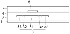
- FIG. 1 is a schematic structural view of fabricating an interlayer insulating layer of the present invention
- FIG. 2 is a schematic structural view of a via hole formed on an interlayer insulating layer of the present invention
- FIG. 3 is a schematic structural view of a source of the present invention.
- FIG. 4 is a schematic structural view of a flat layer, a common electrode, and a passivation layer according to the present invention
- Figure 5 is a schematic view showing the structure of the fifth via hole of the present invention.
- Fig. 6 is a schematic view showing the structure of a pixel electrode of the present invention.
- the array substrate of the present invention comprises a substrate 1, a buffer layer 2, an active layer 3, a gate insulating layer 4, a gate electrode 5, an interlayer insulating layer 6, and an interlayer layer which are sequentially disposed on the substrate 1.
- the common electrode 9 A fourth via 91 is disposed on the active layer 3, and a third via 81 is disposed on the flat via 8 at the fourth via 91.
- the fourth via 91 is disposed on the passivation layer 10.
- the third via hole 81, the flat layer 8, the interlayer insulating layer 6, and the fifth via hole 11 of the gate insulating layer 4 are further provided with a pixel electrode 12 on the passivation layer 10, and the pixel electrode 12 passes through the fifth via hole. 11 is in contact with the active layer 3.
- the active layer 3 includes an undoped layer 31, a heavily doped layer 33 disposed on both sides of the undoped layer 31, and a lightly doped layer 32 disposed between the heavily doped layer 33 and the undoped layer 31.
- the lightly doped layer 32 is an N-type lightly doped layer
- the heavily doped layer 33 is an N-type heavily doped layer, but the invention is not limited thereto, for example, the lightly doped layer 32 may also be a P-type lightly doped layer.
- the impurity layer, the heavily doped layer 33 may also be a P-type heavily doped layer
- the source 7 and the pixel electrode 12 are respectively in contact with the heavily doped layer 33
- the first via 13 and the second via 14 are provided in one of the weights.
- the third via 81, the fourth via 91, and the fifth via 11 are provided at another heavily doped layer 33, which is composed of low temperature polysilicon (Poly-Si).
- the aperture of the first via hole 13 is larger than the aperture of the second via hole 14 and is disposed on the same axis.
- the first via hole 13 and the second via hole 14 are both inverted trapezoidal holes.
- the third via 91 and the fourth via 81 are disposed on the same axis and the aperture of the third via 91 is larger than the aperture of the fourth via 81.
- the fifth via hole 11 is provided by the sixth via hole 41 provided on the gate insulating layer 4, the seventh via hole 61 provided on the interlayer insulating layer 6, and the third via hole 81 provided in the third via hole 81.
- An eight via hole 82, a ninth via hole 92 provided in the fourth via hole 91, and a tenth via hole 101 provided on the passivation layer 10, the sixth via hole 41, the seventh via hole 61, and the The eight vias 82, the ninth vias 92, and the tenth vias 101 are disposed on the same axis; wherein the fifth vias 11 and the third vias 91 and the fourth vias 81 are disposed on the same axis;
- the apertures of the sixth via 41, the seventh via 61, the eighth via 82, the ninth via 92, and the tenth via 101 are equal and smaller than the aperture of the fourth via 81.
- the method for fabricating the array substrate of the present invention comprises the following steps:
- Step one providing a substrate 1;
- the buffer layer 2 is formed on the substrate 1.
- the buffer layer 2 can be fabricated by chemical vapor deposition CVD, and the buffer layer 2 can be a SiN x /SiO x structure, but the invention is not limited thereto, such as buffering.
- Layer 2 can also be a single layer SiN x structure or SiO x structure. ;
- Step 3 forming the active layer 3 on the buffer layer 2, specifically, forming an amorphous silicon layer on the buffer layer 2 by plasma enhanced chemical vapor deposition (PECVD); and then, using the excimer laser
- PECVD plasma enhanced chemical vapor deposition
- the amorphous silicon layer is recrystallized to form an active layer 3 of low temperature polysilicon (Poly-Si).
- the active layer 3 includes an undoped layer 31, a heavily doped layer 33 disposed on both sides of the undoped layer 31, and a lightly doped layer 32 disposed between the heavily doped layer 33 and the undoped layer 31.
- the lightly doped layer 32 is an N-type lightly doped layer
- the heavily doped layer 33 is an N-type heavily doped layer, but the invention is not limited thereto, for example, the lightly doped layer 32 may also be a P-type lightly doped layer.
- the hetero-layer, the heavily doped layer 33 may also be a P-type heavily doped layer;
- the gate insulating layer 4 is formed on the buffer layer 2 and the buffer layer.
- the gate insulating layer 4 may be a SiN x /SiO x structure, but the invention is not limited thereto, for example, the gate insulating layer 4 It may also be a single-layer SiN x structure or a SiO x structure.
- the gate insulating layer 4 can be prepared by chemical vapor deposition CVD, and is not specific here;
- Step 5 forming a gate 5 on the gate insulating layer 4 at the active layer 3.
- the gate 5 faces the undoped layer 31, and the gate 5 may be a molybdenum aluminum molybdenum (MoAlMo) structure or titanium aluminum.
- the titanium (TiAlTi) structure may also be a single-layer molybdenum structure or a single-layer aluminum structure, but the invention is not limited thereto; in the present invention, the gate electrode 5 may be patterned by a physical vapor deposition process to form a gate layer. Process production, but not specific here;
- the interlayer insulating layer 6 is formed on the gate 5 and the gate insulating layer 4.
- the interlayer insulating layer 6 may be a SiN x /SiO x structure, but the invention is not limited thereto.
- the interlayer insulating layer 6 may also be a single-layer SiN x structure or a SiO x structure.
- the interlayer insulating layer 6 may be prepared by chemical vapor deposition CVD, and is not specific here;
- Step 7 as shown in FIG. 2, a first via hole 13 and a second via hole 14 are formed on the interlayer insulating layer 6 and the gate insulating layer 4 is located at one end of the active layer 3, specifically, the first via hole. 13 and a second via 14 is disposed at one of the heavily doped layers 33, and the heavily doped layer 33 is exposed.
- the first via 13 and the second via 14 can be prepared by an etching process, and no specific limited;
- Step 8 As shown in FIG. 3, the source 7 is formed on the interlayer insulating layer 6, and the source 7 is passed through the first via. 13. The second via 14 is in contact with the active layer 3.
- the source 7 may be a molybdenum aluminum molybdenum (MoAlMo) structure or a titanium aluminum titanium (TiAlTi) structure, or may be a single layer molybdenum structure or a single layer.
- the source 7 is in contact with the heavily doped layer 33 via the first via 13 and the second via 14, and the aperture of the first via 13 is larger than the second via 14
- the apertures are disposed on the same axis, and the first vias 13 and the second vias 14 are inverted trapezoidal holes, and the source 7 can be prepared by physical vapor deposition to obtain a source layer and then prepared by a patterning process. No specific limitation is made here;
- Step IX As shown in FIG. 4, a flat layer 8 is formed on the source 7 and on the interlayer insulating layer 6, and a third via 81 is formed on the flat layer 8 at a position opposite to the other end of the active layer 3. Ground, the third via 81 is disposed above the other heavily doped layer 33;
- Step 10 As shown in FIG. 4, the common electrode 9 is formed on the flat layer 8, and the fourth via 91 is formed on the common electrode 9 at the third via 81. Specifically, the aperture of the fourth via 91 is larger than that of the first via 91.
- the apertures of the three via holes 81 are disposed on the same axis; the common electrode 9 is prepared by an etching process after forming a transparent conductive film on the planar layer 8 by physical vapor deposition, which is not specifically limited herein;
- Step 11 As shown in FIG. 4, a passivation layer 10 is formed on the common electrode 9.
- the passivation layer 10 fills the third via 81 and the fourth via 91.
- the passivation layer 10 may be SiN.
- the structure of the passivation layer 10 can be prepared by chemical vapor deposition CVD, which is not specifically limited herein;
- Step 12 as shown in FIG. 5, the fourth via hole 91, the third via hole 81, the interlayer insulating layer 6, and the gate insulating layer 4 are formed on the passivation layer 10 at the fourth via hole 91.
- a fifth via 11, the fifth via 11 and the third via 91 and the fourth via 81 are disposed on the same axis; specifically, the fifth via 11 exposes another heavily doped layer 33,
- the fifth via hole 11 is provided by a sixth via hole 41 provided on the gate insulating layer 4, a seventh via hole 61 provided on the interlayer insulating layer 6, and an eighth via hole 82 provided in the third via hole 81.
- the via hole may be prepared by an etching process, and is not specifically limited herein;
- Step 13 As shown in FIG. 6, the pixel electrode 12 is formed on the passivation layer 10, and the pixel electrode 12 is in contact with the other end of the active layer 4 via the fifth via 11, specifically, the pixel electrode 12 is directly connected to the other
- the heavily doped layer 33 is in contact, and the pixel electrode 12 can be formed by physical vapor deposition of PVD on the passivation layer 10.
- the transparent conductive film After the transparent conductive film is formed on the passivation layer 10, it is prepared by an etching process, which is not limited herein.
- the present invention has only a via hole in one of the heavily doped layers for the connection of the source and the active layer on the interlayer insulating layer, and the other is used for the heavy doping in contact with the pixel electrode.
- the layer is not opened, so that the process from the interlayer insulating layer to the passivation layer is protected, effectively preventing electrostatic discharge of the interlayer insulating layer to the passivation layer process to the active layer to cause electrostatic discharge, thereby causing the active layer to be damaged. This can avoid product performance failure and improve product quality.
Landscapes
- Liquid Crystal (AREA)
- Thin Film Transistor (AREA)
- Devices For Indicating Variable Information By Combining Individual Elements (AREA)
- Internal Circuitry In Semiconductor Integrated Circuit Devices (AREA)
Abstract
一种阵列基板,包括基板(1)、依次设置于基板上的缓冲层(2)、有源层(3)、栅极绝缘层(4)、栅极(5)、层间绝缘层(6)、经层间绝缘层的第一过孔(13)以及栅极绝缘层的第二过孔(14)与有源层接触的源极(7)、平坦层(8)、公共电极(9)、钝化层(10),公共电极上位于有源层处设有第四过孔(91),平坦层上位于第四过孔处设有第三过孔(81),在钝化层上设有贯通第四过孔、第三过孔、平坦层、层间绝缘层、栅极绝缘层的第五过孔(11),在钝化层上还设置有像素电极(12),像素电极经第五过孔与有源层接触。还提供了一种阵列基板的制作方法。与现有技术相比,有效防止在层间绝缘层到钝化层制作中所产生的静电传输至有源层造成静电释放,避免有源层被炸伤,导致产品性能失效的问题,进一步提升产品的品质。
Description
本发明涉及一种显示面板技术,特别是一种低温多晶硅的阵列基板及其制作方法。
在低温多晶硅液晶显示面板(LTPS TFT(thin film transistor)LCD(liquid crystal display))在传统的薄膜晶体管阵列基板的制作工艺流程中,首先于基板上依次制作缓冲层、有源层、栅极绝缘层、栅极、然后制作层间绝缘层并进行蚀刻至有源层的源漏极端的过孔,过孔均将有源层的部分裸露,然后制作源\漏极、制作平坦层、公共电极、钝化层以及像素电极,像素电极与漏极接触;在传统工艺中,用于像素电极与有源层接触的过孔从层间绝缘层开始即成形,在层间绝缘层(ILD)刻蚀后用于与像素电极接触的有源层(poly)为裸露状态;在后面的制程中,如源\漏极(SD)、平坦层(PLN)、公共电极(Com ITO)、钝化层(PV CVD)、像素电极(Pixel ITO),会将产生的静电及易传递至有源层(多晶硅poly Si),从而导致位于层间绝缘层过孔与栅极处的有源层发生静电释放(ESD、Electro-Static discharge)炸伤,造成制程异常,影响产品品质。
发明内容
为克服现有技术的不足,本发明提供一种阵列基板及其制作方法,防止制作中产生的静电传输至有源层造成静电释放,避免产品性能失效,提升产品品质。
本发明提供了一种阵列基板,包括基板、依次设置于基板上的缓冲层、有源层、栅极绝缘层、栅极、层间绝缘层、经层间绝缘层的第一过孔以及栅极绝缘层的第二过孔与有源层接触的源极、平坦层、公共电极、钝化层,所述公共电极上位于有源层处设有第四过孔,平坦层上位于第四过孔处设有第三过孔,在钝化层上设有贯通第四过孔、第三过孔、平坦层、层间绝缘层、栅极绝缘层的第五过孔,在钝化层上还设置有像素电极,所述像素电极经第五过孔与有源层接触。
进一步地,所述第三过孔与第四过孔设置在同一轴线上。
进一步地,所述第五过孔由设于栅极绝缘层上的第六过孔、设于层间绝缘层上的第七过孔、设于第三过孔中的第八过孔、设于第四过孔中的第九过孔以及设于钝化层上的第十过孔构成,所述第六过孔、第七过孔、第八过孔、第九过孔以及第十过孔设置在同一轴线上。
进一步地,所述第五过孔与第三过孔以及第四过孔设置在同一轴线上。
进一步地,所述第六过孔、第七过孔、第八过孔、第九过孔以及第十过孔的孔径相等且小于第四过孔的孔径。
本发明还提供了一种阵列基板的制作方法,包括如下步骤:
提供一基板;
在基板上制作缓冲层;
在缓冲层上制作有源层;
在缓冲层以及缓冲层上制作栅极绝缘层;
在栅极绝缘层上位于有源层处制作栅极;
在栅极以及栅极绝缘层上制作层间绝缘层;
在层间绝缘层上以及栅极绝缘层位于有源层的一端制作有第一过孔、第二过孔;
在层间绝缘层上制作源极,源极经第一过孔、第二过孔与有源层接触;
在源极上以及层间绝缘层上制作平坦层,在平坦层上位于有源层另一端相对的位置处制作第三过孔;
在平坦层上制作公共电极并在公共电极上位于第三过孔处制作第四过孔;
在公共电极上制作钝化层,所述钝化层填充第三过孔、第四过孔;
在钝化层上位于第四过孔处制作贯通第四过孔、第三过孔、层间绝缘层、栅极绝缘层的第五过孔;
在钝化层上制作像素电极,像素电极经第五过孔与有源层的另一端接触。
进一步地,所述第三过孔与第四过孔设置在同一轴线上。
进一步地,所述第五过孔由设于栅极绝缘层上的第六过孔、设于层间绝缘层上的第七过孔、设于第三过孔中的第八过孔、设于第四过孔中的第九过孔以及设于钝化层上的第十过孔构成,所述第六过孔、第七过孔、第八过孔、第九过孔以及第十过孔设置在同一轴线上。
进一步地,所述第五过孔与第三过孔以及第四过孔设置在同一轴线上。
进一步地,所述第六过孔、第七过孔、第八过孔、第九过孔以及第十过孔的孔径相等且小于第四过孔的孔径。
本发明与现有技术相比,通过在制作用于与有源层接触的源漏极时仅制作源极,而用于连接像素电极与有源层的漏极不制作,使得有源层用于连接像素电极的一端从层间绝缘层至钝化层的制作中均被保护起来,从而有效防止在层间绝缘层到钝化层制作中所产生的静电传输至有源层造成静电释放,避免有源层被炸伤,导致产品性能失效的问题,进一步提升产品的品质。
图1是本发明制作层间绝缘层的结构示意图;
图2是本发明在层间绝缘层上制作过孔的结构示意图;
图3是本发明制作源极的结构示意图;
图4是本发明制作平坦层、公共电极以及钝化层的结构示意图;
图5是本发明制作第五过孔的结构示意图;
图6是本发明制作像素电极的结构示意图。
下面结合附图和实施例对本发明作进一步详细说明。
如图6所示,本发明的阵列基板包括基板1、依次设置于基板1上的缓冲层2、有源层3、栅极绝缘层4、栅极5、层间绝缘层6、经层间绝缘层6的第一过孔13以及栅极绝缘层4的第二过孔14与有源层3接触的源极7、平坦层8、公共电极9、钝化层10;所述公共电极9上位于有源层3处设有第四过孔91,平坦层8上位于第四过孔91处设有第三过孔81,在钝化层10上设有贯通第四过孔91、第三过孔81、平坦层8、层间绝缘层6、栅极绝缘层4的第五过孔11,在钝化层10上还设置有像素电极12,所述像素电极12经第五过孔11与有源层3接触。
有源层3包括未掺杂层31、分别设置于未掺杂层31两侧的重掺杂层33及设置于重掺杂层33和未掺杂层31之间的轻掺杂层32。这里,轻掺杂层32为N型轻掺杂层,重掺杂层33为N型重掺杂层,但本发明并不限制于此,例如轻掺杂层32也可以为P型轻掺杂层,重掺杂层33也可以为P型重掺杂层,源极7以及像素电极12分别与重掺杂层33接触,第一过孔13和第二过孔14设于其中一个重掺杂层33处,第三过孔81、第四过孔91及第五过孔11设于另一个重掺杂层33处,所述有源层由低温多晶硅(Poly-Si)构成。
所述第一过孔13的孔径大于第二过孔14的孔径,并且设置在同一轴线上,第一过孔13和第二过孔14均为倒梯形孔。
所述第三过孔91与第四过孔81设置在同一轴线上并且第三过孔91的孔径大于第四过孔81的孔径。
本发明中,第五过孔11由设于栅极绝缘层4上的第六过孔41、设于层间绝缘层6上的第七过孔61、设于第三过孔81中的第八过孔82、设于第四过孔91中的第九过孔92以及设于钝化层10上的第十过孔101构成,所述第六过孔41、第七过孔61、第八过孔82、第九过孔92以及第十过孔101设置在同一轴线上;其中,所述第五过孔11与第三过孔91以及第四过孔81设置在同一轴线上;第六过孔41、第七过孔61、第八过孔82、第九过孔92以及第十过孔101的孔径相等且小于第四过孔81的孔径。
本发明的阵列基板的制作方法包括如下步骤:
步骤一、提供一基板1;
步骤二、在基板1上制作缓冲层2,具体地,缓冲层2可采用化学气相沉积CVD进行制作,缓冲层2可以是SiNx/SiOx结构,但本发明并不限制于此,例如缓冲层2也可以是单层的SiNx结构或SiOx结构。;
步骤三、在缓冲层2上制作有源层3,具体地,利用等离子体增强化学气相沉积法(PECVD)在缓冲层2上制作形成非晶硅层;接着,以利用准分子镭射使所述非晶硅层再结晶,从而生成低温多晶硅(Poly-Si)的有源层3。有源层3包括未掺杂层31、分别设置于未掺杂层31两侧的重掺杂层33及设置于重掺杂层33和未掺杂层31之间的轻掺杂层32。这里,轻掺杂层32为N型轻掺杂层,重掺杂层33为N型重掺杂层,但本发明并不限制于此,例如轻掺杂层32也可以为P型轻掺杂层,重掺杂层33也可以为P型重掺杂层;
步骤四、在缓冲层2以及缓冲层上制作栅极绝缘层4,具体地,栅极绝缘层4可以是SiNx/SiOx结构,但本发明并不限制于此,例如栅极绝缘层4也可以是单层的SiNx结构或SiOx结构,本发明中栅极绝缘层4可采用化学气相沉积CVD制备得到,在此不做具体;
步骤五、在栅极绝缘层4上位于有源层3处制作栅极5,具体地,栅极5正对未掺杂层31,栅极5可以是钼铝钼(MoAlMo)结构或钛铝钛(TiAlTi)结构,也可以是单层的钼结构或者单层的铝结构,但本发明并不限制于此;本发明中栅极5可采用物理气相沉积工艺形成栅极层后通过图形化工艺制作得到,但在此不做具体;
步骤六、如图1所示,在栅极5以及栅极绝缘层4上制作层间绝缘层6,具体地,层间绝缘层6可以是SiNx/SiOx结构,但本发明并不限制于此,例如层间绝缘层6也可以是单层的SiNx结构或SiOx结构,本发明中层间绝缘层6可采用化学气相沉积CVD制备得到,在此不做具体;
步骤七、如图2所示,在层间绝缘层6上以及栅极绝缘层4位于有源层3的一端制作有第一过孔13、第二过孔14,具体地,第一过孔13以及第二过孔14设于其中一重掺杂层33处,并将该重掺杂层33裸露,第一过孔13以及第二过孔14可采用蚀刻工艺制备得到,在此不做具体限定;
步骤八、如图3所示,在层间绝缘层6上制作源极7,源极7经第一过孔
13、第二过孔14与有源层3接触,具体地,源极7可采用钼铝钼(MoAlMo)结构或钛铝钛(TiAlTi)结构,也可以是单层的钼结构或者单层的铝结构,但本发明并不限制于此;所述源极7经第一过孔13、第二过孔14与重掺杂层33接触,第一过孔13的孔径大于第二过孔14的孔径,并且设置在同一轴线上,第一过孔13和第二过孔14均为倒梯形孔,所述源极7可采用物理气相沉积制作得到源极层后通过图形化工艺制备得到,在此不做具体限定;
步骤九、如图4所示,在源极7上以及层间绝缘层6上制作平坦层8,在平坦层8上位于有源层3另一端相对的位置处制作第三过孔81,具体地,第三过孔81设置在另一个重掺杂层33上方;
步骤十、如图4所示,在平坦层8上制作公共电极9并在公共电极9上位于第三过孔81处制作第四过孔91,具体地,第四过孔91的孔径大于第三过孔81的孔径且两者设置在同一轴线上;公共电极9通过在物理气相沉积在平坦层8上形成透明导电膜后通过蚀刻工艺制备得到,在此不做具体限定;
步骤十一、如图4所示,在公共电极9上制作钝化层10,所述钝化层10填充第三过孔81、第四过孔91,具体地,钝化层10可以是SiNx结构,钝化层10可通过化学气相沉积CVD制备得到,在此不作具体限定;
步骤十二、如图5所示,在钝化层10上位于第四过孔91处制作贯通第四过孔91、第三过孔81、层间绝缘层6、栅极绝缘层4的第五过孔11,所述第五过孔11与第三过孔91以及第四过孔81设置在同一轴线上;具体地,第五过孔11将另一个重掺杂层33裸露,所述第五过孔11由设于栅极绝缘层4上的第六过孔41、设于层间绝缘层6上的第七过孔61、设于第三过孔81中的第八过孔82、设于第四过孔91中的第九过孔92以及设于钝化层10上的第十过孔101构成,所述第六过孔41、第七过孔61、第八过孔82、第九过孔92以及第十过孔101设置在同一轴线上,第六过孔41、第七过孔61、第八过孔82、第九过孔92以及第十过孔101的孔径相等且小于第四过孔81的孔径,上述过孔可通过蚀刻工艺制备得到,在此不做具体限定;
步骤十三、如图6所示,在钝化层10上制作像素电极12,像素电极12经第五过孔11与有源层4的另一端接触,具体地,像素电极12直接与另一个重掺杂层33接触,像素电极12可通过在钝化层10上以物理气相沉积PVD制
备方法在钝化层10上形成透明导电膜后通过蚀刻工艺制备得到,在此不做限定。
本发明与传统的LTPS工艺结构相比,在层间绝缘层上仅在其中一重掺杂层开设过孔用于源极与有源层的连接,另一个用于与像素电极接触的重掺杂层不开孔,从而在层间绝缘层至钝化层制程均被保护,有效防止层间绝缘层至钝化层制程的静电传输至有源层造成静电释放从而导致将有源层炸伤,这样能够避免产品性能失效,提升产品品质。
虽然已经参照特定实施例示出并描述了本发明,但是本领域的技术人员将理解:在不脱离由权利要求及其等同物限定的本发明的精神和范围的情况下,可在此进行形式和细节上的各种变化。
Claims (16)
- 一种阵列基板,其中:包括基板、依次设置于基板上的缓冲层、有源层、栅极绝缘层、栅极、层间绝缘层、经层间绝缘层的第一过孔以及栅极绝缘层的第二过孔与有源层接触的源极、平坦层、公共电极、钝化层,所述公共电极上位于有源层处设有第四过孔,平坦层上位于第四过孔处设有第三过孔,在钝化层上设有贯通第四过孔、第三过孔、平坦层、层间绝缘层、栅极绝缘层的第五过孔,在钝化层上还设置有像素电极,所述像素电极经第五过孔与有源层接触。
- 根据权利要求1所述的阵列基板,其中:所述第三过孔与第四过孔设置在同一轴线上。
- 根据权利要求1所述的阵列基板,其中:所述第五过孔由设于栅极绝缘层上的第六过孔、设于层间绝缘层上的第七过孔、设于第三过孔中的第八过孔、设于第四过孔中的第九过孔以及设于钝化层上的第十过孔构成,所述第六过孔、第七过孔、第八过孔、第九过孔以及第十过孔设置在同一轴线上。
- 根据权利要求2所述的阵列基板,其中:所述第五过孔由设于栅极绝缘层上的第六过孔、设于层间绝缘层上的第七过孔、设于第三过孔中的第八过孔、设于第四过孔中的第九过孔以及设于钝化层上的第十过孔构成,所述第六过孔、第七过孔、第八过孔、第九过孔以及第十过孔设置在同一轴线上。
- 根据权利要求3所述的阵列基板,其中:所述第五过孔与第三过孔以及第四过孔设置在同一轴线上。
- 根据权利要求4所述的阵列基板,其中:所述第五过孔与第三过孔(91)以及第四过孔设置在同一轴线上。
- 根据权利要求5所述的阵列基板,其中:所述第六过孔、第七过孔、第八过孔、第九过孔以及第十过孔的孔径相等且小于第四过孔的孔径。
- 根据权利要求6所述的阵列基板,其中:所述第六过孔、第七过孔、第八过孔、第九过孔以及第十过孔的孔径相等且小于第四过孔的孔径。
- 一种阵列基板的制作方法,其中:包括如下步骤:提供一基板;在基板上制作缓冲层;在缓冲层上制作有源层;在缓冲层以及缓冲层上制作栅极绝缘层;在栅极绝缘层上位于有源层处制作栅极;在栅极以及栅极绝缘层上制作层间绝缘层;在层间绝缘层上以及栅极绝缘层位于有源层的一端制作有第一过孔、第二过孔;在层间绝缘层上制作源极,源极经第一过孔、第二过孔与有源层接触;在源极上以及层间绝缘层上制作平坦层,在平坦层上位于有源层另一端相对的位置处制作第三过孔;在平坦层上制作公共电极并在公共电极上位于第三过孔处制作第四过孔;在公共电极上制作钝化层,所述钝化层填充第三过孔、第四过孔;在钝化层上位于第四过孔处制作贯通第四过孔、第三过孔、层间绝缘层、栅极绝缘层的第五过孔;在钝化层上制作像素电极,像素电极经第五过孔与有源层的另一端接触。
- 根据权利要求9所述的阵列基板的制作方法,其中:所述第三过孔与第四过孔设置在同一轴线上。
- 根据权利要求9所述的阵列基板的制作方法,其中:所述第五过孔由设于栅极绝缘层上的第六过孔、设于层间绝缘层上的第七过孔、设于第三过孔中的第八过孔、设于第四过孔中的第九过孔以及设于钝化层上的第十过孔构成,所述第六过孔、第七过孔、第八过孔、第九过孔以及第十过孔设置在同一 轴线上。
- 根据权利要求10所述的阵列基板的制作方法,其中:所述第五过孔由设于栅极绝缘层上的第六过孔、设于层间绝缘层上的第七过孔、设于第三过孔中的第八过孔、设于第四过孔中的第九过孔以及设于钝化层上的第十过孔构成,所述第六过孔、第七过孔、第八过孔、第九过孔以及第十过孔设置在同一轴线上。
- 根据权利要求11所述的阵列基板的制作方法,其中:所述第五过孔与第三过孔以及第四过孔设置在同一轴线上。
- 根据权利要求12所述的阵列基板的制作方法,其中:所述第五过孔与第三过孔以及第四过孔设置在同一轴线上。
- 根据权利要求13所述的阵列基板的制作方法,其中:所述第六过孔、第七过孔、第八过孔、第九过孔以及第十过孔的孔径相等且小于第四过孔的孔径。
- 根据权利要求14所述的阵列基板的制作方法,其中:所述第六过孔、第七过孔、第八过孔、第九过孔以及第十过孔的孔径相等且小于第四过孔的孔径。
Priority Applications (1)
| Application Number | Priority Date | Filing Date | Title |
|---|---|---|---|
| US15/577,705 US10553616B2 (en) | 2017-07-24 | 2017-09-06 | Array substrate and method of manufacturing the same |
Applications Claiming Priority (2)
| Application Number | Priority Date | Filing Date | Title |
|---|---|---|---|
| CN201710606999.8 | 2017-07-24 | ||
| CN201710606999.8A CN107240590B (zh) | 2017-07-24 | 2017-07-24 | 阵列基板及其制作方法 |
Publications (1)
| Publication Number | Publication Date |
|---|---|
| WO2019019278A1 true WO2019019278A1 (zh) | 2019-01-31 |
Family
ID=59988013
Family Applications (1)
| Application Number | Title | Priority Date | Filing Date |
|---|---|---|---|
| PCT/CN2017/100718 Ceased WO2019019278A1 (zh) | 2017-07-24 | 2017-09-06 | 阵列基板及其制作方法 |
Country Status (3)
| Country | Link |
|---|---|
| US (1) | US10553616B2 (zh) |
| CN (1) | CN107240590B (zh) |
| WO (1) | WO2019019278A1 (zh) |
Cited By (1)
| Publication number | Priority date | Publication date | Assignee | Title |
|---|---|---|---|---|
| CN110993620A (zh) * | 2019-12-05 | 2020-04-10 | 深圳市华星光电半导体显示技术有限公司 | 阵列基板及其制备方法、显示面板 |
Families Citing this family (3)
| Publication number | Priority date | Publication date | Assignee | Title |
|---|---|---|---|---|
| CN114137771B (zh) * | 2021-12-08 | 2023-08-01 | Tcl华星光电技术有限公司 | 阵列基板及其制作方法 |
| WO2023184402A1 (zh) * | 2022-03-31 | 2023-10-05 | 京东方科技集团股份有限公司 | 显示基板及其制作方法、显示面板 |
| CN114784113B (zh) * | 2022-04-02 | 2025-08-12 | 深圳市华星光电半导体显示技术有限公司 | 显示面板及显示装置 |
Citations (3)
| Publication number | Priority date | Publication date | Assignee | Title |
|---|---|---|---|---|
| CN105140244A (zh) * | 2015-09-25 | 2015-12-09 | 武汉华星光电技术有限公司 | 阵列基板及其制造方法、显示装置 |
| CN106158882A (zh) * | 2016-09-27 | 2016-11-23 | 厦门天马微电子有限公司 | 一种显示装置、显示面板、阵列基板及其制作方法 |
| CN106847743A (zh) * | 2017-02-07 | 2017-06-13 | 武汉华星光电技术有限公司 | Tft基板及其制作方法 |
Family Cites Families (3)
| Publication number | Priority date | Publication date | Assignee | Title |
|---|---|---|---|---|
| JP4818839B2 (ja) * | 2006-07-19 | 2011-11-16 | 株式会社 日立ディスプレイズ | 液晶表示装置及びその製造方法 |
| CN105679765A (zh) * | 2016-01-12 | 2016-06-15 | 武汉华星光电技术有限公司 | Tft阵列基板结构 |
| CN105446000B (zh) * | 2016-01-21 | 2018-07-10 | 武汉华星光电技术有限公司 | 护眼式液晶显示装置的制作方法 |
-
2017
- 2017-07-24 CN CN201710606999.8A patent/CN107240590B/zh active Active
- 2017-09-06 WO PCT/CN2017/100718 patent/WO2019019278A1/zh not_active Ceased
- 2017-09-06 US US15/577,705 patent/US10553616B2/en active Active
Patent Citations (3)
| Publication number | Priority date | Publication date | Assignee | Title |
|---|---|---|---|---|
| CN105140244A (zh) * | 2015-09-25 | 2015-12-09 | 武汉华星光电技术有限公司 | 阵列基板及其制造方法、显示装置 |
| CN106158882A (zh) * | 2016-09-27 | 2016-11-23 | 厦门天马微电子有限公司 | 一种显示装置、显示面板、阵列基板及其制作方法 |
| CN106847743A (zh) * | 2017-02-07 | 2017-06-13 | 武汉华星光电技术有限公司 | Tft基板及其制作方法 |
Cited By (1)
| Publication number | Priority date | Publication date | Assignee | Title |
|---|---|---|---|---|
| CN110993620A (zh) * | 2019-12-05 | 2020-04-10 | 深圳市华星光电半导体显示技术有限公司 | 阵列基板及其制备方法、显示面板 |
Also Published As
| Publication number | Publication date |
|---|---|
| US20190081074A1 (en) | 2019-03-14 |
| US10553616B2 (en) | 2020-02-04 |
| CN107240590B (zh) | 2020-01-17 |
| CN107240590A (zh) | 2017-10-10 |
Similar Documents
| Publication | Publication Date | Title |
|---|---|---|
| US9478562B2 (en) | Array substrate and manufacturing method thereof, display device, thin film transistor and manufacturing method thereof | |
| US10795478B2 (en) | Array substrate and preparation method therefor, and display apparatus | |
| KR101710179B1 (ko) | 평판 표시 장치 및 그 제조 방법 | |
| KR102169014B1 (ko) | 박막트랜지스터 어레이 기판 및 그 제조방법 | |
| US8198631B2 (en) | Display device and method of fabricating the same | |
| US7057675B2 (en) | Liquid crystal display device and the fabricating method thereof comprising pixel electrode completely covering adjacent gate line and adjacent channel region unconnected to the pixel electrode | |
| US7999262B2 (en) | Thin film transistor, method of fabricating the same, and method of fabricating liquid crystal display device having the same | |
| US20140117370A1 (en) | Array substrate, display device and manufacturing method thereof | |
| WO2018188146A1 (zh) | 一种阵列基板、显示装置及其制作方法 | |
| US20150295094A1 (en) | Thin film transistor, manufacturing method thereof, array substrate and display device | |
| WO2015074420A1 (zh) | 阵列基板及其制备方法和显示装置 | |
| CN107240590B (zh) | 阵列基板及其制作方法 | |
| WO2015096307A1 (zh) | 氧化物薄膜晶体管、显示器件、及阵列基板的制造方法 | |
| US10290665B2 (en) | Array substrates, display devices, and the manufacturing methods thereof | |
| US20240355840A1 (en) | Array substrate and manufacturing method thereof, and display panel | |
| CN109545820B (zh) | 显示装置和制造该显示装置的方法 | |
| US7638371B2 (en) | Method for manufacturing thin film transistor display array with dual-layer metal line | |
| WO2014172957A1 (zh) | 电路板、其制作方法以及显示装置 | |
| CN110854113B (zh) | 静电防护结构、制造方法以及阵列基板母板 | |
| TWI469356B (zh) | 薄膜電晶體及其製造方法 | |
| WO2021103142A1 (zh) | 一种显示面板及其制作方法及电子设备 | |
| CN108321122B (zh) | Cmos薄膜晶体管及其制备方法和显示装置 | |
| CN103151253B (zh) | 信号线的制作方法、薄膜晶体管、阵列基板及显示装置 | |
| US8329518B1 (en) | Methods for manufacturing thin film transistor array substrate and display panel | |
| KR100787805B1 (ko) | 화소 구조의 제조 방법 |
Legal Events
| Date | Code | Title | Description |
|---|---|---|---|
| 121 | Ep: the epo has been informed by wipo that ep was designated in this application |
Ref document number: 17919545 Country of ref document: EP Kind code of ref document: A1 |
|
| NENP | Non-entry into the national phase |
Ref country code: DE |
|
| 122 | Ep: pct application non-entry in european phase |
Ref document number: 17919545 Country of ref document: EP Kind code of ref document: A1 |