WO2019013131A1 - プレーナ型トランス及びdcdcコンバータ - Google Patents
プレーナ型トランス及びdcdcコンバータ Download PDFInfo
- Publication number
- WO2019013131A1 WO2019013131A1 PCT/JP2018/025717 JP2018025717W WO2019013131A1 WO 2019013131 A1 WO2019013131 A1 WO 2019013131A1 JP 2018025717 W JP2018025717 W JP 2018025717W WO 2019013131 A1 WO2019013131 A1 WO 2019013131A1
- Authority
- WO
- WIPO (PCT)
- Prior art keywords
- planar
- air core
- primary side
- core coil
- secondary side
- Prior art date
- Legal status (The legal status is an assumption and is not a legal conclusion. Google has not performed a legal analysis and makes no representation as to the accuracy of the status listed.)
- Ceased
Links
Images




Classifications
-
- H—ELECTRICITY
- H01—ELECTRIC ELEMENTS
- H01F—MAGNETS; INDUCTANCES; TRANSFORMERS; SELECTION OF MATERIALS FOR THEIR MAGNETIC PROPERTIES
- H01F38/00—Adaptations of transformers or inductances for specific applications or functions
- H01F38/08—High-leakage transformers or inductances
-
- H—ELECTRICITY
- H01—ELECTRIC ELEMENTS
- H01F—MAGNETS; INDUCTANCES; TRANSFORMERS; SELECTION OF MATERIALS FOR THEIR MAGNETIC PROPERTIES
- H01F27/00—Details of transformers or inductances, in general
- H01F27/28—Coils; Windings; Conductive connections
- H01F27/2804—Printed windings
-
- H—ELECTRICITY
- H01—ELECTRIC ELEMENTS
- H01F—MAGNETS; INDUCTANCES; TRANSFORMERS; SELECTION OF MATERIALS FOR THEIR MAGNETIC PROPERTIES
- H01F27/00—Details of transformers or inductances, in general
- H01F27/28—Coils; Windings; Conductive connections
- H01F27/32—Insulating of coils, windings, or parts thereof
- H01F27/324—Insulation between coil and core, between different winding sections, around the coil; Other insulation structures
- H01F27/326—Insulation between coil and core, between different winding sections, around the coil; Other insulation structures specifically adapted for discharge lamp ballasts
-
- H—ELECTRICITY
- H01—ELECTRIC ELEMENTS
- H01F—MAGNETS; INDUCTANCES; TRANSFORMERS; SELECTION OF MATERIALS FOR THEIR MAGNETIC PROPERTIES
- H01F27/00—Details of transformers or inductances, in general
- H01F27/34—Special means for preventing or reducing unwanted electric or magnetic effects, e.g. no-load losses, reactive currents, harmonics, oscillations, leakage fields
- H01F27/346—Preventing or reducing leakage fields
-
- H—ELECTRICITY
- H01—ELECTRIC ELEMENTS
- H01F—MAGNETS; INDUCTANCES; TRANSFORMERS; SELECTION OF MATERIALS FOR THEIR MAGNETIC PROPERTIES
- H01F3/00—Cores, Yokes, or armatures
- H01F3/10—Composite arrangements of magnetic circuits
- H01F3/14—Constrictions; Gaps, e.g. air-gaps
-
- H—ELECTRICITY
- H02—GENERATION; CONVERSION OR DISTRIBUTION OF ELECTRIC POWER
- H02M—APPARATUS FOR CONVERSION BETWEEN AC AND AC, BETWEEN AC AND DC, OR BETWEEN DC AND DC, AND FOR USE WITH MAINS OR SIMILAR POWER SUPPLY SYSTEMS; CONVERSION OF DC OR AC INPUT POWER INTO SURGE OUTPUT POWER; CONTROL OR REGULATION THEREOF
- H02M3/00—Conversion of DC power input into DC power output
- H02M3/01—Resonant DC/DC converters
-
- H—ELECTRICITY
- H02—GENERATION; CONVERSION OR DISTRIBUTION OF ELECTRIC POWER
- H02M—APPARATUS FOR CONVERSION BETWEEN AC AND AC, BETWEEN AC AND DC, OR BETWEEN DC AND DC, AND FOR USE WITH MAINS OR SIMILAR POWER SUPPLY SYSTEMS; CONVERSION OF DC OR AC INPUT POWER INTO SURGE OUTPUT POWER; CONTROL OR REGULATION THEREOF
- H02M3/00—Conversion of DC power input into DC power output
- H02M3/22—Conversion of DC power input into DC power output with intermediate conversion into AC
- H02M3/24—Conversion of DC power input into DC power output with intermediate conversion into AC by static converters
- H02M3/28—Conversion of DC power input into DC power output with intermediate conversion into AC by static converters using discharge tubes with control electrode or semiconductor devices with control electrode to produce the intermediate AC
- H02M3/325—Conversion of DC power input into DC power output with intermediate conversion into AC by static converters using discharge tubes with control electrode or semiconductor devices with control electrode to produce the intermediate AC using devices of a triode or a transistor type requiring continuous application of a control signal
- H02M3/335—Conversion of DC power input into DC power output with intermediate conversion into AC by static converters using discharge tubes with control electrode or semiconductor devices with control electrode to produce the intermediate AC using devices of a triode or a transistor type requiring continuous application of a control signal using semiconductor devices only
- H02M3/33569—Conversion of DC power input into DC power output with intermediate conversion into AC by static converters using discharge tubes with control electrode or semiconductor devices with control electrode to produce the intermediate AC using devices of a triode or a transistor type requiring continuous application of a control signal using semiconductor devices only having several active switching elements
- H02M3/33571—Half-bridge at primary side of an isolation transformer
-
- H—ELECTRICITY
- H02—GENERATION; CONVERSION OR DISTRIBUTION OF ELECTRIC POWER
- H02M—APPARATUS FOR CONVERSION BETWEEN AC AND AC, BETWEEN AC AND DC, OR BETWEEN DC AND DC, AND FOR USE WITH MAINS OR SIMILAR POWER SUPPLY SYSTEMS; CONVERSION OF DC OR AC INPUT POWER INTO SURGE OUTPUT POWER; CONTROL OR REGULATION THEREOF
- H02M3/00—Conversion of DC power input into DC power output
- H02M3/22—Conversion of DC power input into DC power output with intermediate conversion into AC
- H02M3/24—Conversion of DC power input into DC power output with intermediate conversion into AC by static converters
- H02M3/28—Conversion of DC power input into DC power output with intermediate conversion into AC by static converters using discharge tubes with control electrode or semiconductor devices with control electrode to produce the intermediate AC
- H02M3/325—Conversion of DC power input into DC power output with intermediate conversion into AC by static converters using discharge tubes with control electrode or semiconductor devices with control electrode to produce the intermediate AC using devices of a triode or a transistor type requiring continuous application of a control signal
- H02M3/335—Conversion of DC power input into DC power output with intermediate conversion into AC by static converters using discharge tubes with control electrode or semiconductor devices with control electrode to produce the intermediate AC using devices of a triode or a transistor type requiring continuous application of a control signal using semiconductor devices only
- H02M3/33569—Conversion of DC power input into DC power output with intermediate conversion into AC by static converters using discharge tubes with control electrode or semiconductor devices with control electrode to produce the intermediate AC using devices of a triode or a transistor type requiring continuous application of a control signal using semiconductor devices only having several active switching elements
- H02M3/33576—Conversion of DC power input into DC power output with intermediate conversion into AC by static converters using discharge tubes with control electrode or semiconductor devices with control electrode to produce the intermediate AC using devices of a triode or a transistor type requiring continuous application of a control signal using semiconductor devices only having several active switching elements having at least one active switching element at the secondary side of an isolation transformer
-
- H—ELECTRICITY
- H01—ELECTRIC ELEMENTS
- H01F—MAGNETS; INDUCTANCES; TRANSFORMERS; SELECTION OF MATERIALS FOR THEIR MAGNETIC PROPERTIES
- H01F27/00—Details of transformers or inductances, in general
- H01F27/28—Coils; Windings; Conductive connections
- H01F27/2804—Printed windings
- H01F2027/2819—Planar transformers with printed windings, e.g. surrounded by two cores and to be mounted on printed circuit
-
- H—ELECTRICITY
- H02—GENERATION; CONVERSION OR DISTRIBUTION OF ELECTRIC POWER
- H02M—APPARATUS FOR CONVERSION BETWEEN AC AND AC, BETWEEN AC AND DC, OR BETWEEN DC AND DC, AND FOR USE WITH MAINS OR SIMILAR POWER SUPPLY SYSTEMS; CONVERSION OF DC OR AC INPUT POWER INTO SURGE OUTPUT POWER; CONTROL OR REGULATION THEREOF
- H02M1/00—Details of apparatus for conversion
- H02M1/0048—Circuits or arrangements for reducing losses
- H02M1/0054—Transistor switching losses
- H02M1/0058—Transistor switching losses by employing soft switching techniques, i.e. commutation of transistors when applied voltage is zero or when current flow is zero
-
- H—ELECTRICITY
- H02—GENERATION; CONVERSION OR DISTRIBUTION OF ELECTRIC POWER
- H02M—APPARATUS FOR CONVERSION BETWEEN AC AND AC, BETWEEN AC AND DC, OR BETWEEN DC AND DC, AND FOR USE WITH MAINS OR SIMILAR POWER SUPPLY SYSTEMS; CONVERSION OF DC OR AC INPUT POWER INTO SURGE OUTPUT POWER; CONTROL OR REGULATION THEREOF
- H02M1/00—Details of apparatus for conversion
- H02M1/0064—Magnetic structures combining different functions, e.g. storage, filtering or transformation
-
- H—ELECTRICITY
- H02—GENERATION; CONVERSION OR DISTRIBUTION OF ELECTRIC POWER
- H02M—APPARATUS FOR CONVERSION BETWEEN AC AND AC, BETWEEN AC AND DC, OR BETWEEN DC AND DC, AND FOR USE WITH MAINS OR SIMILAR POWER SUPPLY SYSTEMS; CONVERSION OF DC OR AC INPUT POWER INTO SURGE OUTPUT POWER; CONTROL OR REGULATION THEREOF
- H02M3/00—Conversion of DC power input into DC power output
- H02M3/003—Constructional details, e.g. physical layout, assembly, wiring or busbar connections
Definitions
- the present invention relates to a planar transformer.
- the above-described transformer is mainly configured to actively generate a leakage inductance on the secondary side, there is a possibility that a sufficient leakage inductance can not be secured when viewed as a whole of the transformer.
- the present invention has been made in view of the above-described circumstances, and an object of the present invention is to ensure sufficient leakage inductance.
- the planar type transformer according to one aspect of the present invention is disposed at a distance from the planar air core coil on the primary side and the planar air core coil on the primary side in the winding center axis direction of the planar air core coil on the primary side.
- a planar air core coil on the secondary side having a non-facing portion not facing the planar air core coil on the primary side in the winding central axis direction, a planar air core coil on the primary side in the winding central axis direction and a planar surface on the secondary side
- FIG. 1 is a circuit diagram showing a DCDC converter using a planar transformer according to an embodiment of the present invention.
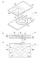
- 2A and 2B show the basic configuration of a planar type transformer constituting the transformer of FIG. 1, wherein FIG. 2A is an exploded perspective view, FIG. 2B is a side view, and FIG. 2C is a plan view.
- FIG. 3 (a) is an explanatory view showing a leakage inductance and an excitation inductance generated in the planar air core coil of the primary side and the secondary side of the planar type transformer arranged in FIG. 2, and FIG. It is explanatory drawing which shows the leakage inductance and excitation inductance which arise in the planar air core coil of the primary side and secondary side which were made to match.
- FIG. 3 (a) is an explanatory view showing a leakage inductance and an excitation inductance generated in the planar air core coil of the primary side and the secondary side of the planar type transformer arranged in FIG. 2, and FIG. It is ex
- FIG. 4 is a graph showing the correlation between the magnitudes of leakage inductance and excitation inductance generated in the planar air core coil on the primary side and the secondary side of FIG. 2 and the deviation of the winding central axis of both planar air core coils.
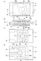
- FIG. 5 shows a specific configuration of a planar type transformer used as the transformer of FIG. 1, where (a) is a plan view, (b) is a cross-sectional view taken along the line II of (a), and (c) is a first order
- FIG. 7D is a plan view showing the front surface side of the substrate on which the side planar core is formed, and FIG. 7D is a plan view showing the back surface side of the substrate on which the secondary side planar core is formed.
- FIG. 6 is a cross-sectional view of a planar type transformer used as the transformer of FIG. 1 in which the size of the planar air core coil differs between the primary side and the secondary side.
- FIG. 1 is a circuit diagram showing a DCDC converter using a planar transformer according to an embodiment of the present invention.
- the DCDC converter 1 of the present embodiment shown in FIG. 1 is an isolated DCDC converter using an asymmetric half bridge LLC converter 3 on the primary side of a transformer T.
- the DC-DC converter 1 converts the direct-current voltage Vin input to the primary side into alternating current by switching of the semiconductor elements Q1 and Q2 configured with the MOSFET of the LLC converter 3 and the like, and coils on the primary and secondary sides of the transformer T After boosting between Np and Ns, the voltage is returned to direct current by the rectifying diodes D1 and D2 and the smoothing capacitor Co, and is supplied to the load Ro on the secondary side.
- switching loss in the LLC converter 3 is suppressed by alternately turning on and off the semiconductor elements Q1 and Q2 in the cycle of the resonance frequency of the series resonance circuit of the leakage inductance of the primary coil Np and the resonance capacitor Cr.
- the DC voltage Vin can be boosted with high efficiency.
- the DCDC converter 1 is constituted by a resonant circuit, and turns on and off the semiconductor elements Q1 and Q2 at a high frequency (at least 1 MHz as the high frequency referred to here). Also, in order to establish a resonant circuit at a high frequency, a very small excitation inductance (for example, 0.8 ⁇ H for driving at 2 MHz) and a large leakage inductance (for example, 1.1 ⁇ H for driving at 2 MHz) are required. .
- a planar transformer is used as the transformer T.
- the configuration of the planar transformer will be described with reference to FIG. 2A and 2B show the basic configuration of the planar type transformer that constitutes the transformer T, wherein (a) is an exploded perspective view, (b) is a side view, and (c) is a plan view.
- the planar type transformer Tp in the example shown in FIG. 2A is configured of a primary side planar core Cp made of a magnetic material, a metal primary side planar air core coil Nap laminated thereon, and a magnetic material. And the metallic secondary side planar air core coil Nas stacked on the secondary side planar core Cs.
- planar air core coil Nap on the primary side and the planar air core coil Nas on the secondary side are formed in an annular shape having the same diameter, and are disposed non-coaxially.
- planar core Cp on the primary side and the planar core Cs on the secondary side are formed in a rectangular shape of the same size.
- the planar core Cp on the primary side and the planar core Cs on the secondary side have an outer diameter larger than the outer diameters of the planar air core coil Nap on the primary side and the planar air core coil Nas on the secondary side.
- the planar core Cp on the primary side is disposed to face the planar core Cs on the secondary side at an interval. Then, the planar air core coil Nap on the primary side and the planar air core coil Nas on the secondary side are respectively stacked on mutually opposing surfaces of the planar core Cp on the primary side and the planar core Cs on the secondary side.
- planar air core coil Nap on the primary side and the planar air core coil Nas on the secondary side are the spacing direction between the planar core Cp on the primary side and the planar core Cs on the secondary side, that is, the respective winding central axes Sp, There is a gap in the axial direction of Ss.
- the planar air core coil Nap on the primary side and the planar air core coil Nas on the secondary side wind the positions of the winding central axes Sp and Ss such that the air cores Ap and As partially overlap with each other. They are arranged to be shifted in the radial direction orthogonal to the line central axes Sp and Ss.
- the primary side flat air core coil Nap overlaps the secondary side flat air core coil Nas in the radial direction of the winding central axis Sp.
- a facing portion Fp and a non-facing portion NFp located on the outside of the planar air core coil Nas on the secondary side are provided.
- an opposing portion Fs overlapping the planar air core coil Nap on the primary side in the radial direction of the winding central axis Ss and the outside of the planar air core coil Nap on the primary side A non-facing portion NFs located is provided.
- the explanatory view of FIG. As shown in the diagram, between the two planar air core coils Nap and Nas, the excitation inductance Lm is generated in the facing portions Fp and Fs, and the leakage inductance Lr is generated in the non-facing portions NFp and NFs.
- FIG. 3A a planar type in which the winding central axis Sp of the primary side flat air core coil Nap and the winding central axis Ss of the secondary side flat air core coil Nas are mutually offset.
- the transformer Tp is a coaxial planar type transformer in which the winding central axis Sp of the primary side flat air core coil Nap and the winding central axis Ss of the secondary side flat air core coil Nas shown in FIG. 3B overlap.
- the transformer T of FIG. 1 is more suitable than the transformer Tp as a transformer T for causing the leakage inductance of the primary side coil Np to be in series resonance with the resonance capacitor Cr.
- a leakage inductance Lr having a size that resonates in series with the resonance capacitor Cr of FIG. 1 between the two planar air core coils Nap and Nas of the primary side and the secondary side of FIG.
- a planar type transformer Tp having a displacement amount that produces an excitation inductance Lm of a size that satisfies the necessary coupling coefficient between the coils Np and Ns on the secondary side is used as the transformer T in FIG.
- the amount of deviation between the primary and secondary planar air core coils Nap and Nas for obtaining a desired leakage inductance Lr can be set to a range in which at least the outer edges of the two overlap each other. .
- 5 (a) is a plan view of the planar transformer Tp
- (b) is a cross-sectional view taken along the line II of (a)
- (c) is a plan view showing the surface side of the substrate on which the planar core of the primary side is formed.
- (D) is a top view which shows the back surface side of the board
- the planar type transformer Tp of this embodiment shown in FIG. 5 (a) is a plane empty on the primary side between the front surface 51 and the back surface 53, as shown in FIG. 5 (b) which is a sectional view taken along the line II of FIG. It has the board
- the substrate 5 is rigidly formed of, for example, an insulating resin material such as glass epoxy.
- the primary side flat air core coil Nap formed on the surface 51 of the substrate 5 has terminal portions Rp provided on both ends of the conductor looped in a square shape, the long sides of the surface 51 It is extended to the side.
- the secondary side flat air core coil Nas formed on the back surface 53 of the substrate 5 is, as shown in FIG. 5 (d), a primary side looped in a square shape. Terminal portions Rs provided at both ends of a conductor having the same shape as the planar air core coil Nap are extended to the short side of the back surface 53.
- both the terminal portions Rp and Rs are magnetic circuits.
- the planar transformer Tp configured as described above is used as the transformer T of the LLC converter 3
- the planar air core coil Nap on the primary side and the planar air core on the secondary side are used.
- the deviation between the planar air core coil Nap on the primary side and the planar air core coil Nas on the secondary side means the deviation of the center of both windings.
- a leakage inductance Lr of a size large enough to cause series resonance with the large capacity resonance capacitor Cr matched to the semiconductor elements Q1 and Q2 switching at high frequency is generated in the planar transformer Tp.
- the LLC converter 3 can be driven at high frequency.
- planar core Cp on the primary side It is possible to eliminate the need to process the structure of the planar transformer Tp including the planar core Cs of the secondary side and the secondary side with high accuracy.
- planar core Cp on the primary side and the planar core Cs on the secondary side have a center pole inserted into the air cores Ap and As of the planar air core coil Nap on the primary side and the planar air core coil Nas on the secondary side. I did not. Therefore, the biplanar cores Cp and Cs sandwich the air cores Ap and As of the primary and secondary flat air core coils Nap and Nas, and the winding central axes Sp and Ss of the flat air core coils Nap and Nas. It is arranged to face each other at intervals in the axial direction of.
- the magnetic flux passing through the planar air core coil Nap on the primary side and the planar air core coil Nas on the secondary side is the planar core Cp on the primary side and the planar core Cs on the secondary side. There is no concentration.
- the center pole inserted into the air cores Ap and As of the planar air core coils Nap and Nas on the primary side and the secondary side is a planar core on the primary side.
- the planar core Cp on the primary side and the planar core Cs on the secondary side may be configured by an EE core or an EI core by providing the planar core Cs on the Cp or secondary side.
- the planar core Cp on the primary side and the planar core Cs on the secondary side of the planar transformer Tp can be replaced by the planar air core coil Nap on the primary side and the planar air core on the secondary side.
- the outer diameter of the coil Nas was larger than the outer diameter.
- planar core Cp on the primary side and the planar core Cs on the secondary side may have an outer diameter smaller than the outer diameter of the planar air core coil Nap on the primary side and the planar air core coil Nas on the secondary side.
- planar air core coil Nap on the primary side of the planar transformer Tp and the planar air core coil Nas on the secondary side have the same shape except for the terminal portions Rp and Rs.
- the sizes of the planar air core coils Nap and Nas may be made different between the primary side and the secondary side, or the planar air core coils Nap and Nas may be different on the primary side
- the number of turns of the core coils Nap and Nas may be made different.
- planar air core coil Nap on the primary side and the planar air core coil Nas on the secondary side can be formed by etching or the like, and the respective positions can be processed with high accuracy. Then, when performing such processing, a reference portion (for example, a through hole) may be opened somewhere on the substrate 5.
- planar air core coil Nas on the secondary side it is processed so as to shift the winding center of the planar air core coil Nas by a predetermined distance from the reference portion, and the primary side is formed.
- the deviation accuracy between the planar air core coil Nap and the planar air core coil Nas on the secondary side can be increased.
- the present invention is not limited to the transformer of the isolated DC-DC converter using the asymmetric half bridge LLC converter, and can be widely applied to various transformers used in the field utilizing leakage inductance.
- One aspect of the present invention can be used in various transformers used in the field utilizing leakage inductance.
Landscapes
- Engineering & Computer Science (AREA)
- Power Engineering (AREA)
- Chemical & Material Sciences (AREA)
- Composite Materials (AREA)
- Dc-Dc Converters (AREA)
Priority Applications (2)
| Application Number | Priority Date | Filing Date | Title |
|---|---|---|---|
| CN201880046635.1A CN110914938B (zh) | 2017-07-14 | 2018-07-06 | 平面型变压器和dcdc转换器 |
| US16/630,071 US11404202B2 (en) | 2017-07-14 | 2018-07-06 | Planar transformer and DC-DC converter |
Applications Claiming Priority (2)
| Application Number | Priority Date | Filing Date | Title |
|---|---|---|---|
| JP2017-137997 | 2017-07-14 | ||
| JP2017137997A JP6895832B2 (ja) | 2017-07-14 | 2017-07-14 | プレーナ型トランス及びdcdcコンバータ |
Publications (1)
| Publication Number | Publication Date |
|---|---|
| WO2019013131A1 true WO2019013131A1 (ja) | 2019-01-17 |
Family
ID=65002656
Family Applications (1)
| Application Number | Title | Priority Date | Filing Date |
|---|---|---|---|
| PCT/JP2018/025717 Ceased WO2019013131A1 (ja) | 2017-07-14 | 2018-07-06 | プレーナ型トランス及びdcdcコンバータ |
Country Status (4)
| Country | Link |
|---|---|
| US (1) | US11404202B2 (https=) |
| JP (1) | JP6895832B2 (https=) |
| CN (1) | CN110914938B (https=) |
| WO (1) | WO2019013131A1 (https=) |
Families Citing this family (6)
| Publication number | Priority date | Publication date | Assignee | Title |
|---|---|---|---|---|
| JP7182513B2 (ja) * | 2019-05-24 | 2022-12-02 | 株式会社Soken | 磁気部品及びこれを備えた電力変換装置 |
| JP7779650B2 (ja) | 2020-11-19 | 2025-12-03 | 株式会社京三製作所 | スイッチングモジュール |
| US11631523B2 (en) * | 2020-11-20 | 2023-04-18 | Analog Devices International Unlimited Company | Symmetric split planar transformer |
| CN114496518B (zh) * | 2021-12-28 | 2025-08-08 | 深圳顺络电子股份有限公司 | 一种立式多相电感器及其制造方法 |
| CN114864238B (zh) * | 2022-04-25 | 2025-03-18 | 武汉大学 | 一种用于太赫兹谐波提取的片上低插损双频变压器 |
| US20240339262A1 (en) * | 2023-04-07 | 2024-10-10 | Murata Manufacturing Co., Ltd. | Magnetic component |
Citations (3)
| Publication number | Priority date | Publication date | Assignee | Title |
|---|---|---|---|---|
| JPH05326295A (ja) * | 1992-05-15 | 1993-12-10 | Matsushita Electric Works Ltd | 平面型トランス |
| JP2000243637A (ja) * | 1999-02-23 | 2000-09-08 | Nec Kansai Ltd | 薄型インダクタ及びこれを用いた薄型dc−dcコンバータ |
| JP2013080881A (ja) * | 2011-10-05 | 2013-05-02 | Tdk Corp | コイル部品 |
Family Cites Families (7)
| Publication number | Priority date | Publication date | Assignee | Title |
|---|---|---|---|---|
| JPS57152110A (en) * | 1981-03-17 | 1982-09-20 | Kourin Giken:Kk | Composite coil |
| JPS61188338U (https=) | 1985-05-16 | 1986-11-25 | ||
| JP4175367B2 (ja) * | 2003-08-11 | 2008-11-05 | サンケン電気株式会社 | スイッチング電源装置 |
| JP4391314B2 (ja) * | 2004-05-10 | 2009-12-24 | パナソニック株式会社 | 高周波加熱装置 |
| KR101122983B1 (ko) * | 2007-02-20 | 2012-03-15 | 세이코 엡슨 가부시키가이샤 | 코일 유닛 및 전자 기기 |
| JP2009267077A (ja) * | 2008-04-25 | 2009-11-12 | Seiko Epson Corp | コイルユニット及びそれを用いた電子機器 |
| CN101630578A (zh) * | 2008-07-22 | 2010-01-20 | 光诠科技股份有限公司 | 高压可调漏磁变压器 |
-
2017
- 2017-07-14 JP JP2017137997A patent/JP6895832B2/ja not_active Expired - Fee Related
-
2018
- 2018-07-06 WO PCT/JP2018/025717 patent/WO2019013131A1/ja not_active Ceased
- 2018-07-06 US US16/630,071 patent/US11404202B2/en active Active
- 2018-07-06 CN CN201880046635.1A patent/CN110914938B/zh not_active Expired - Fee Related
Patent Citations (3)
| Publication number | Priority date | Publication date | Assignee | Title |
|---|---|---|---|---|
| JPH05326295A (ja) * | 1992-05-15 | 1993-12-10 | Matsushita Electric Works Ltd | 平面型トランス |
| JP2000243637A (ja) * | 1999-02-23 | 2000-09-08 | Nec Kansai Ltd | 薄型インダクタ及びこれを用いた薄型dc−dcコンバータ |
| JP2013080881A (ja) * | 2011-10-05 | 2013-05-02 | Tdk Corp | コイル部品 |
Also Published As
| Publication number | Publication date |
|---|---|
| CN110914938B (zh) | 2022-09-20 |
| US11404202B2 (en) | 2022-08-02 |
| JP2019021733A (ja) | 2019-02-07 |
| US20200211765A1 (en) | 2020-07-02 |
| CN110914938A (zh) | 2020-03-24 |
| JP6895832B2 (ja) | 2021-06-30 |
Similar Documents
| Publication | Publication Date | Title |
|---|---|---|
| CN110914938B (zh) | 平面型变压器和dcdc转换器 | |
| US8570133B2 (en) | Transformer | |
| CN108962556B (zh) | 变压器和具有所述变压器的llc谐振转换器 | |
| US11398344B2 (en) | Transformer | |
| JP2008205466A (ja) | 磁気部品 | |
| WO2020071512A1 (ja) | 巻鉄心及び変圧器 | |
| CN107924755B (zh) | 变压器及具备其的谐振电路 | |
| JP2014063856A (ja) | 複合磁性部品及びスイッチング電源装置 | |
| CN104025213A (zh) | 电感性组件和使用 | |
| CN110635663B (zh) | 集成磁组合件和将其组装的方法 | |
| JP4287495B1 (ja) | 三相高周波トランス | |
| KR20140041867A (ko) | 리액터 및 전기 기기 | |
| JP2009059995A (ja) | 複合磁気部品 | |
| US20110032062A1 (en) | Transformer improved in leakage inductance | |
| US8970339B2 (en) | Integrated magnetic assemblies and methods of assembling same | |
| JP2011077255A (ja) | 電源用薄形トランス | |
| JP2008166624A (ja) | トランス及びそれを用いた共振型スイッチング電源 | |
| JP2009105180A (ja) | トランス | |
| US20240290536A1 (en) | Cellular flyback transformer | |
| CN103137303B (zh) | 一种提高气隙磁芯电感系数的方法 | |
| JP2018067660A (ja) | トランス及び電力変換装置 | |
| US20190013138A1 (en) | Core for transformer or reactor | |
| JP2008159817A (ja) | リアクトル及びこれを用いた電源装置 | |
| JP2008270347A (ja) | トランス | |
| JP2022150081A (ja) | リーケージトランス |
Legal Events
| Date | Code | Title | Description |
|---|---|---|---|
| 121 | Ep: the epo has been informed by wipo that ep was designated in this application |
Ref document number: 18831906 Country of ref document: EP Kind code of ref document: A1 |
|
| DPE1 | Request for preliminary examination filed after expiration of 19th month from priority date (pct application filed from 20040101) | ||
| NENP | Non-entry into the national phase |
Ref country code: DE |
|
| 122 | Ep: pct application non-entry in european phase |
Ref document number: 18831906 Country of ref document: EP Kind code of ref document: A1 |