WO2019012934A1 - デジタルアンプおよび出力装置 - Google Patents
デジタルアンプおよび出力装置 Download PDFInfo
- Publication number
- WO2019012934A1 WO2019012934A1 PCT/JP2018/023505 JP2018023505W WO2019012934A1 WO 2019012934 A1 WO2019012934 A1 WO 2019012934A1 JP 2018023505 W JP2018023505 W JP 2018023505W WO 2019012934 A1 WO2019012934 A1 WO 2019012934A1
- Authority
- WO
- WIPO (PCT)
- Prior art keywords
- signal
- amplifier
- digital
- pulse width
- output
- Prior art date
- Legal status (The legal status is an assumption and is not a legal conclusion. Google has not performed a legal analysis and makes no representation as to the accuracy of the status listed.)
- Ceased
Links
Images

Classifications
-
- H—ELECTRICITY
- H03—ELECTRONIC CIRCUITRY
- H03F—AMPLIFIERS
- H03F3/00—Amplifiers with only discharge tubes or only semiconductor devices as amplifying elements
- H03F3/20—Power amplifiers, e.g. Class B amplifiers, Class C amplifiers
- H03F3/21—Power amplifiers, e.g. Class B amplifiers, Class C amplifiers with semiconductor devices only
- H03F3/217—Class D power amplifiers; Switching amplifiers
-
- H—ELECTRICITY
- H03—ELECTRONIC CIRCUITRY
- H03F—AMPLIFIERS
- H03F3/00—Amplifiers with only discharge tubes or only semiconductor devices as amplifying elements
- H03F3/181—Low-frequency amplifiers, e.g. audio preamplifiers
-
- H—ELECTRICITY
- H03—ELECTRONIC CIRCUITRY
- H03F—AMPLIFIERS
- H03F3/00—Amplifiers with only discharge tubes or only semiconductor devices as amplifying elements
- H03F3/20—Power amplifiers, e.g. Class B amplifiers, Class C amplifiers
- H03F3/21—Power amplifiers, e.g. Class B amplifiers, Class C amplifiers with semiconductor devices only
- H03F3/217—Class D power amplifiers; Switching amplifiers
- H03F3/2175—Class D power amplifiers; Switching amplifiers using analogue-digital or digital-analogue conversion
-
- H—ELECTRICITY
- H03—ELECTRONIC CIRCUITRY
- H03F—AMPLIFIERS
- H03F3/00—Amplifiers with only discharge tubes or only semiconductor devices as amplifying elements
- H03F3/50—Amplifiers in which input is applied to, or output is derived from, an impedance common to input and output circuits of the amplifying element, e.g. cathode follower
-
- H—ELECTRICITY
- H03—ELECTRONIC CIRCUITRY
- H03F—AMPLIFIERS
- H03F3/00—Amplifiers with only discharge tubes or only semiconductor devices as amplifying elements
- H03F3/68—Combinations of amplifiers, e.g. multi-channel amplifiers for stereophonics
-
- H—ELECTRICITY
- H03—ELECTRONIC CIRCUITRY
- H03H—IMPEDANCE NETWORKS, e.g. RESONANT CIRCUITS; RESONATORS
- H03H11/00—Networks using active elements
- H03H11/02—Multiple-port networks
- H03H11/04—Frequency selective two-port networks
- H03H11/12—Frequency selective two-port networks using amplifiers with feedback
- H03H11/126—Frequency selective two-port networks using amplifiers with feedback using a single operational amplifier
-
- H—ELECTRICITY
- H03—ELECTRONIC CIRCUITRY
- H03K—PULSE TECHNIQUE
- H03K7/00—Modulating pulses with a continuously-variable modulating signal
- H03K7/08—Duration or width modulation ; Duty cycle modulation
-
- H—ELECTRICITY
- H03—ELECTRONIC CIRCUITRY
- H03M—CODING; DECODING; CODE CONVERSION IN GENERAL
- H03M1/00—Analogue/digital conversion; Digital/analogue conversion
- H03M1/06—Continuously compensating for, or preventing, undesired influence of physical parameters
- H03M1/0617—Continuously compensating for, or preventing, undesired influence of physical parameters characterised by the use of methods or means not specific to a particular type of detrimental influence
- H03M1/0634—Continuously compensating for, or preventing, undesired influence of physical parameters characterised by the use of methods or means not specific to a particular type of detrimental influence by averaging out the errors, e.g. using sliding scale
- H03M1/0636—Continuously compensating for, or preventing, undesired influence of physical parameters characterised by the use of methods or means not specific to a particular type of detrimental influence by averaging out the errors, e.g. using sliding scale in the amplitude domain
- H03M1/0639—Continuously compensating for, or preventing, undesired influence of physical parameters characterised by the use of methods or means not specific to a particular type of detrimental influence by averaging out the errors, e.g. using sliding scale in the amplitude domain using dither, e.g. using triangular or sawtooth waveforms
-
- H—ELECTRICITY
- H03—ELECTRONIC CIRCUITRY
- H03F—AMPLIFIERS
- H03F2200/00—Indexing scheme relating to amplifiers
- H03F2200/03—Indexing scheme relating to amplifiers the amplifier being designed for audio applications
-
- H—ELECTRICITY
- H03—ELECTRONIC CIRCUITRY
- H03F—AMPLIFIERS
- H03F3/00—Amplifiers with only discharge tubes or only semiconductor devices as amplifying elements
- H03F3/20—Power amplifiers, e.g. Class B amplifiers, Class C amplifiers
- H03F3/21—Power amplifiers, e.g. Class B amplifiers, Class C amplifiers with semiconductor devices only
- H03F3/217—Class D power amplifiers; Switching amplifiers
- H03F3/2171—Class D power amplifiers; Switching amplifiers with field-effect devices
-
- H—ELECTRICITY
- H03—ELECTRONIC CIRCUITRY
- H03F—AMPLIFIERS
- H03F3/00—Amplifiers with only discharge tubes or only semiconductor devices as amplifying elements
- H03F3/20—Power amplifiers, e.g. Class B amplifiers, Class C amplifiers
- H03F3/21—Power amplifiers, e.g. Class B amplifiers, Class C amplifiers with semiconductor devices only
- H03F3/217—Class D power amplifiers; Switching amplifiers
- H03F3/2173—Class D power amplifiers; Switching amplifiers of the bridge type
Definitions
- One embodiment of the present invention relates to a digital amplifier whose input signal is a digital signal and an output device using the digital amplifier.
- a digital audio reproduction system includes a DA converter (quantizer), and a digital signal system and an analog signal system are mixed.
- Patent Document 1 describes a digital amplifier that adds an output of a switching circuit and an output of an LC filter that receives the output as an input, and inputs the addition result to an LPF on a feedback loop.
- Patent Document 2 discloses digital switching in which each of the 1-bit signals subjected to delta sigma modulation is attenuated and an adjustment voltage is added so that the DC voltage level difference between the negative feedback signals to the delta sigma modulation circuit becomes zero. An amplifier is described.
- Patent Document 3 a digital switching amplifier is provided on a feedback loop that feeds a switching signal back to the delta sigma modulation unit, and a digital switching amplifier provided with a decompression unit that decompresses the switching signal by resistance division to generate a feedback signal.
- a digital switching amplifier provided with a decompression unit that decompresses the switching signal by resistance division to generate a feedback signal.
- Patent Document 4 describes a signal correction device that adjusts a pulse width based on a feedback signal based on an output signal of a switching circuit that amplifies an output signal of a pulse width adjustment circuit.
- Japanese Patent Publication No. Japanese Patent Application Laid-Open No. 2007-5957 (released on January 11, 2007)" Japanese Patent Laid-Open Publication No. 2001-32939 (published on November 30, 2001) Japanese Patent Laid-Open Publication No. 2000-295049 (October 20, 2000) Japanese Patent Laid-Open Publication No. 2010-268211 (released on November 25, 2010)
- the present invention has been made in view of the above problems, and an object thereof is to provide a technology for realizing a digital amplifier using a feedback signal or a dither signal with minimizing and limiting an analog signal system. It is in.
- a digital amplifier includes a pulse width adjustment circuit that adjusts a pulse width of a digital signal, a switching circuit that amplifies an output signal of the pulse width adjustment circuit, and And a feedback signal generation unit that generates a feedback signal based on an output signal of the switching circuit, wherein the pulse width adjustment circuit adjusts the pulse width of the digital signal with reference to the feedback signal, and the feedback signal generation unit
- a first amplifier for outputting a first amplified signal obtained by amplifying the difference between the output signal of the switching circuit and one of the reference voltage and the dither signal; and the other of the first amplified signal, the dither signal and the reference voltage
- a second amplifier for amplifying the difference between the signal and the output signal, and outputting the amplified difference as the feedback signal.
- an output device includes a first digital amplifier for amplifying a first digital signal, and a second of a phase opposite to that of the first digital signal.
- a first digital amplifier for amplifying a digital signal of the first digital amplifier comprising: a first pulse width adjusting circuit for adjusting a pulse width of the first digital signal;
- a first switching circuit for amplifying an output signal of the adjustment circuit, and a first feedback signal generating unit for generating a first feedback signal based on the output signal of the first switching circuit,
- the pulse width adjustment circuit adjusts the pulse width of the first digital signal with reference to the first feedback signal, and the first feedback signal generator further includes the first switch.
- a first amplifier for outputting a first amplified signal obtained by amplifying the difference between the output signal of the output circuit and one of the reference voltage and the dither signal, and the difference between the first amplified signal and the other of the dither signal and the reference voltage
- a second amplifier for outputting the amplified difference as the first feedback signal, and the second digital amplifier adjusts the pulse width of the second digital signal.
- a second switching circuit for amplifying an output signal of the second pulse width adjusting circuit, and a second feedback signal generating circuit based on an output signal of the second switching circuit.
- the second pulse width adjustment circuit adjusts the pulse width of the second digital signal with reference to the second feedback signal, and And a third amplifier for outputting a third amplified signal obtained by amplifying the difference between the output signal of the second switching circuit and one of the reference voltage and the dither signal, and the third amplified signal. And a fourth amplifier for amplifying the difference between the signal and the other of the dither signal and the reference voltage and outputting the amplified difference as the second feedback signal.
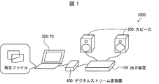
- FIG. 1 is a conceptual view of a digital audio reproduction system including an output device according to Embodiment 1 of the present invention.
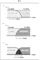
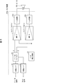
- FIG. 1 is a block diagram showing a main configuration of an output device according to Embodiment 1 of the present invention. It is a figure which shows the frequency characteristic of the filter of the output device which concerns on Embodiment 1 of this invention. It is a block diagram of the output device which carried out BTL connection of the digital amplifier concerning Embodiment 2 of this invention.
- Embodiment 1 Hereinafter, embodiments of the present invention will be described in detail.
- FIG. 1 is a conceptual view of a digital audio reproduction system 1000 including an output device 100 according to an embodiment of the present invention. As shown in FIG. 1, the digital audio reproduction system 1000 includes an output device 100, a speaker 200, a personal computer (PC) 300, and a digital stream converter 400, which will be described later.
- PC personal computer
- the PC 300 outputs the reproduction data of the reproduction file as a serial digital signal encoded.
- the digital stream converter 400 outputs, to the output device 100, a DSD signal obtained by digitizing the encoded serial digital signal acquired from the PC 300 in accordance with the Direct Stream Digital (DSD) conversion method.
- DSD Direct Stream Digital
- the output device 100 amplifies the acquired digital signal and outputs the amplified signal to the speaker 200.
- the speaker 200 outputs a sound based on the signal output from the output device 100.
- the digital audio reproduction system 1000 can output reproduction data of a reproduction file reproduced by the PC 300 from the speaker 200.
- FIG. 2 is a block diagram showing the main configuration of the output device 100 according to the embodiment of the present invention.
- the output device 100 includes differential receivers 10 and 12, digital sampling 14, a dither generation circuit (dither signal generation circuit) 16, a digital amplifier 1, and a filter circuit 42.
- the digital signal of the input signal is input to the differential receiver 10 through two signal lines, and a digital signal is output according to the difference between the two signal lines.
- the clock signal is input to the differential receiver 12 through two signal lines, and the clock signal is output according to the difference between the two signal lines.
- the digital signal output from the differential receiver 10 and the clock signal output from the differential receiver 12 are input to the digital sampling 14, and digital sampling is performed according to the digital signal and the clock signal.
- the dither generation circuit 16 outputs a dither signal for suppressing noise of the signal output from the digital amplifier 1.
- the dither generation circuit 16 outputs a triangular wave or white noise.
- the frequency of the dither signal output from the dither generation circuit 16 is a frequency other than an integral multiple of the sampling frequency of the digital signal input to the digital amplifier 1.
- the digital amplifier 1 receives a digital signal output from the digital sampling 14 as an input signal.
- the digital amplifier 1 outputs a digital signal obtained by amplifying the input digital signal to the filter circuit 42.
- the digital amplifier 1 includes a pulse width modulator (pulse width adjustment circuit) 18, a switching circuit module 20, a dead time generator 26, a variable voltage source 28, an attenuator 30, a current monitoring circuit 32, and a feedback signal generation unit 40. ing.
- the pulse width modulator 18 adjusts the pulse width of the digital signal output from the digital sampling 14, and outputs the adjusted digital signal to the switching circuit module 20.
- the switching circuit module 20 includes a gate drive circuit 22 and a switching circuit 24.
- the switching circuit module 20 amplifies the voltage of the digital signal output from the pulse width modulator 18 according to the power supply voltage output from the variable voltage source 28, and outputs the amplified digital signal.
- the dead time generator 26 generates a dead time for adjusting the timing for driving the switching circuit 24.
- the variable voltage source 28 is a voltage source for supplying a power supply voltage for amplifying the voltage by the switching circuit module 20 and a reference voltage to be described later. By varying the variable voltage source 28, the output voltage of the switching circuit module 20 is adjusted.
- the attenuator 30 is an attenuator for adjusting the reference voltage.
- the current monitoring circuit 32 is a protection circuit that monitors the current flowing through the switching circuit 24.
- the feedback signal generation unit 40 generates a feedback signal based on the output signal of the switching circuit module 20, the dither signal, and the reference voltage, and outputs the feedback signal to the pulse width modulator 18.
- the feedback signal generation unit 40 includes an attenuator 34, a first stage amplifier 36, and a second stage amplifier 38, as shown in FIG.
- the feedback signal generation unit 40 generates three signals of the output signal of the switching circuit module 20, the power supply voltage from the variable voltage source 28, and the dither signal output from the dither generation circuit 16 into the pulse width give feedback. In other words, the feedback signal generation unit 40 feeds back the pulse width adjustment signal to the pulse width modulator 18 according to the three parameters of the output signal, the power supply voltage, and the dither signal.
- the pulse width modulator 18 adjusts the pulse width of the digital signal with reference to the feedback signal.
- the attenuator 34 outputs an output signal obtained by attenuating the output from the switching circuit module 20.
- the first stage amplifier 36 outputs a first amplified signal obtained by amplifying the difference between the output signal from the attenuator 34 and the reference voltage from the variable voltage source 28.
- the feedback by the first stage amplifier 36 can suppress distortion of the output signal of the switching circuit module 20 caused by load fluctuation of the power supply voltage output from the variable voltage source 28. Further, the first stage amplifier 36 can suppress the DC component of the output signal, which contributes to noise reduction. Further, the response to the voltage fluctuation is improved by the output of the first stage amplifier 36, so that the braking characteristic of the output signal is increased.
- the first stage amplifier 36 contributes to the reduction of analog noise caused by fluctuation of the power supply voltage generated inside the circuit of the digital amplifier 1 and digital noise caused by the generation of dead time.
- the second stage amplifier 38 amplifies the difference between the dither signal from the dither generation circuit 16 and the first amplified signal, and outputs the amplified difference to the pulse width modulator 18 as a feedback signal.
- the second stage amplifier 38 contributes to the reduction of noise due to the quantization error of the digital signal by the dither signal.
- the second stage amplifier 38 breaks up the frequency distribution of non-periodic noise such as white noise and can disperse the noise component.
- the frequency of the triangular wave output from the dither generation circuit 16 be an integral multiple of the sampling frequency in order to prevent beat interference.
- the noise generated by the quantization error has a frequency component in the audible range, it becomes a noise source to be heard.
- the periodicity of this noise can be reduced by the input of the dither signal. For example, to suppress noise having random frequency components, it is effective to input a triangular wave signal exceeding the audible range.
- the frequency of the noise can be broken and noise can be dispersed.
- white noise input having various frequency components is effective for suppressing pink noise having a certain periodicity. Since the periodicity of pink noise can be broken by white noise, the influence of noise can be suppressed.
- At least one of the first stage amplifier 36 and the second stage amplifier 38 can function as a filter. Then, in view of Example 2 to be described later, the frequency characteristics of at least one of the filter functions of the first stage amplifier 36 and the second stage amplifier 38 are changed in order to suppress only specific noise.
- FIG. 3 shows an example of a filter in the case of applying feedback to a low frequency region.
- the first stage amplifier 36 does not function as a filter
- the second stage amplifier 38 functions as a low pass filter.
- first stage amplifier 36 and the second stage amplifier 38 may function as a low pass filter
- first stage amplifier 36 may function as a low pass filter
- second stage amplifier 38 may function as a filter. It does not have to be.
- both the first stage amplifier 36 and the second stage amplifier 38 may function as a low pass filter.
- FIG. 3 shows an example of a filter in the case of applying feedback to a high frequency region.
- the first stage amplifier 36 does not function as a filter
- the second stage amplifier 38 functions as a high pass filter.
- feedback can be applied only to relatively high frequency regions, and low frequency noise components can be removed.
- at least one of the first stage amplifier 36 and the second stage amplifier 38 only needs to function as a high pass filter, and the first stage amplifier 36 functions as a high pass filter, and the second stage amplifier 38 functions as a filter It does not have to be.
- both the first stage amplifier 36 and the second stage amplifier 38 may function as a high pass filter.
- FIG. 3 shows an example of a filter in the case of applying feedback to a specific frequency region.
- the first stage amplifier 36 functions as a low pass filter
- the second stage amplifier 38 functions as a high pass filter.
- feedback can be applied only to a specific frequency region like a band pass filter, and specific noise components can be removed.
- One of the first stage amplifier 36 and the second stage amplifier 38 may be made to function as a low pass filter, and the other may be made to function as a high pass filter, and the first stage amplifier 36 be made to function as a high pass filter.
- the eye amplifier 38 may function as a low pass filter.
- the amplifier function as a filter, the degree of freedom of feedback can be expanded.
- the gains of the first stage amplifier 36 and the second stage amplifier 38 can be changed.
- the present invention is not limited to this configuration. That is, a dither signal may be input to the first stage amplifier 36 and a reference voltage may be input to the second stage amplifier 38.
- the first stage amplifier 36 outputs a first amplified signal obtained by amplifying the difference between the output signal of the switching circuit 24 and the dither signal
- the second stage amplifier 38 outputs the first amplified signal and the reference voltage. The difference between the two signals is amplified, and the amplified difference is output as a feedback signal.
- the first stage amplifier 36 may output a first amplified signal obtained by amplifying the difference between the output signal of the switching circuit module 20 and one of the reference voltage and the dither signal.
- the second stage amplifier 38 may amplify the difference between the first amplification signal and the other of the dither signal and the reference voltage, and output the amplified difference as a feedback signal.
- the filter circuit 42 is composed of an inductor and a capacitor, and extracts a desired frequency component.
- the digital amplifier 1 By connecting the filter circuit 42 to the digital amplifier 1, the digital amplifier 1 can amplify the input audio signal and output it as a digital signal for driving the speaker 200.
- FIG. 4 is a block diagram of an output device 100a in which the digital amplifier 1 according to the first embodiment of the present invention is BTL connected.
- the output device 100 a includes differential receivers 10 and 12, digital sampling 14, a dither generation circuit 16, a digital amplifier (first digital amplifier) 1 a that amplifies a first digital signal, and a filter circuit 42 a. And a digital amplifier (second digital amplifier) 1b for amplifying a second digital signal in reverse phase to the first digital signal, and a filter circuit 42b.
- the output of the digital sampling 14 and the output of the dither generation circuit 16 are input to each of the digital amplifier 1a and the digital amplifier 1b.
- a filter circuit 42a is connected to the output side of the digital amplifier 1a.
- a filter circuit 42 b is connected to the output side of the digital amplifier 1 b.
- a speaker 200 (load) is connected to the output side of the filter circuit 42a and the filter circuit 42b.
- the output device 100 a can amplify an audio signal, which is an input digital signal, and output an audio from the speaker 200.
- the digital sampling 14 uses a flip flop, and outputs a first digital signal (Q) and a second digital signal (a signal in reverse phase of Q).
- the first digital signal (Q) is output to the digital amplifier 1a
- the second digital signal (signal in reverse phase of Q) is output to the digital amplifier 1b.
- the digital sampling 14 can output a signal of positive phase to the digital amplifier 1a, and can output a signal of reverse phase opposite to the signal output to the digital amplifier 1a to the digital amplifier 1b. . With this configuration, it is possible to cancel DC components of the output signals of the digital amplifier 1a and the digital amplifier 1b.
- the dither generation circuit 16 outputs an in-phase signal to the digital amplifier 1a and the digital amplifier 1b. With this configuration, the respective dither signals of the digital amplifier 1a and the digital amplifier 1b can also be canceled out at the output.
- the digital amplifier 1 a and the digital amplifier 1 b are BTL connected. Therefore, the output device 100a can realize a digital amplifier whose output voltage is doubled.
- Example 1 Full digital amplifier with DSD signal as sound source
- a full digital amplifier that amplifies a DSD signal as it is a digital signal
- digital noise not included in the original DSD signal source is generated.
- a DC dither signal was input to operate feedback by applying a DC voltage.
- the input of the direct current dither signal contributes to the suppression of the offset voltage of the output, and the noise of the output signal is suppressed.
- Example 2 Frter function of amplifier
- a low pass filter having a cutoff frequency of 30 Hz was applied to the amplifier.
- feedback can be applied only to the offset voltage having a component of 30 Hz or less that causes noise, and noise can be removed without affecting the output signal.
- the digital amplifiers 1, 1a and 1b include a pulse width adjustment circuit (pulse width modulator 18) for adjusting the pulse width of a digital signal, and the pulse width adjustment circuit (pulse width modulator 18).
- a switching circuit 24 for amplifying an output signal
- a feedback signal generation unit 40 for generating a feedback signal based on the output signal of the switching circuit 24.
- the pulse width adjusting circuit (pulse width modulator 18) The pulse width of the digital signal is adjusted with reference to the signal, and the feedback signal generation unit 40 amplifies a difference between the output signal of the switching circuit 24 and one of the reference voltage and the dither signal.
- a first amplifier for outputting, and the other of the first amplification signal, the dither signal and the reference voltage
- the difference was amplified and the amplified the difference comprises a, a second amplifier that outputs (second stage amplifier 38) as the feedback signal.
- the first amplifier (first stage amplifier 36) amplifies the difference between the output signal of the switching circuit 24 and the reference voltage
- the second amplifier amplifies the difference between the first amplification signal and the dither signal, and uses the amplified difference as the feedback signal. You may output it.
- the digital signal at the input can be appropriately fed back, and noise in the output signal of the switching circuit can be appropriately eliminated.
- the frequency characteristic of the first amplifier is in the audible frequency range (.about.20 kHz)
- the frequency characteristic of the second amplifier for injecting the dither signal is a band where the dither signal frequency can sufficiently pass (a band wider than the audible frequency).
- the digital amplifiers 1, 1a and 1b according to aspect 3 of the present invention further include a dither signal generation circuit (dither generation circuit 16) that generates the dither signal in the above aspect 1 or 2, and the dither signal generation circuit (dither The generation circuit 16) may output a triangular wave or white noise.
- dither generation circuit 16 a dither signal generation circuit that generates the dither signal in the above aspect 1 or 2
- the dither signal generation circuit may output a triangular wave or white noise.
- the frequency of the dither signal may be a frequency other than an integral multiple of the sampling frequency of the digital signal.
- the digital amplifiers 1, 1a and 1b according to aspect 5 of the present invention are the same as the aspects 1 to 4 in at least at least the first amplifier (first stage amplifier 36) and the second amplifier (second stage amplifier 38).
- One may function as a filter.
- the digital amplifiers 1, 1a and 1b according to aspect 6 of the present invention are the same as the aspects 1 to 5 described above in that the first amplifier (first stage amplifier 36) and the second amplifier (second stage amplifier 38) are It may function as a low pass filter.
- the digital amplifiers 1, 1a and 1b according to aspect 7 of the present invention are the same as the above-mentioned aspects 1 to 5, wherein the first amplifier (first stage amplifier 36) and the second amplifier (second stage amplifier 38) are It may function as a high pass filter.
- feedback can be applied only to a relatively high frequency region, and low frequency noise components can be removed.
- the digital amplifiers 1, 1a and 1b according to the eighth aspect of the present invention are the same as the first amplifier (first stage amplifier 36) and the second amplifier (second stage amplifier 38) in the first to fifth aspects. , One may function as a low pass filter and the other may function as a high pass filter.
- An output device 100a amplifies a first digital amplifier (digital amplifier 1a) for amplifying a first digital signal, and a second digital signal in reverse phase to the first digital signal.
- a first digital amplifier (digital amplifier 1b), and the first digital amplifier (digital amplifier 1a) is a first pulse width adjustment circuit (pulse width) for adjusting the pulse width of the first digital signal.
- the generation unit 40) outputs a first amplified signal obtained by amplifying the difference between the output signal of the first switching circuit (switching circuit 24) and one of the reference voltage and the dither signal (first stage)
- a second amplifier (a second stage amplifier) which amplifies the difference between the amplifier 36) and the other of the first amplified signal and the dither signal and the other of the reference voltage and outputs the amplified difference as the first feedback signal 38), and the second digital amplifier (digital amplifier 1b) is a
- a modulator 18 a second switching circuit (switching circuit 24) for amplifying an output signal of the second pulse width adjusting circuit (pulse width modulator 18), and the second switching circuit (switching circuit 24) And a second feedback signal generation unit (feedback signal generation unit 40) for generating a second feedback signal based on the output signal from the second pulse width adjustment circuit (pulse width modulator 18).
- the pulse width of the second digital signal is adjusted with reference to a second feedback signal, and the second feedback signal generation unit (feedback signal generation unit 40) adjusts the second switching circuit (switching circuit 24).
- Third amplifier (a first stage) that outputs a third amplified signal obtained by amplifying the difference between the output signal of the reference signal and one of the reference voltage and the dither signal
- a fourth amplifier (second stage amplifier) which amplifies the difference between the amplifier 36) and the other of the third amplified signal and the dither signal and the reference voltage and outputs the amplified difference as the second feedback signal 38) and.
- the output device 100a can realize a digital amplifier in which the output voltage is doubled.
Landscapes
- Engineering & Computer Science (AREA)
- Power Engineering (AREA)
- Theoretical Computer Science (AREA)
- Multimedia (AREA)
- Amplifiers (AREA)
Abstract
アナログ信号系を最小かつ限定的にして、フィードバック信号やディザ信号を用いたデジタルアンプを実現する。デジタル信号のパルス幅を調整するパルス幅変調器(18)と、パルス幅変調器(18)の出力信号を増幅するスイッチング回路(24)と、スイッチング回路(24)の出力信号に基づいてフィードバック信号を生成する減衰器(34)とを備え、パルス幅変調器(18)は、フィードバック信号を参照してデジタル信号のパルス幅を調整し、減衰器(34)は、スイッチング回路(24)の出力信号と基準電圧およびディザ信号の一方との差分を増幅した第1の増幅信号を出力する第1の増幅器(36)と、第1の増幅信号とディザ信号および基準電圧の他方との差分を増幅し、増幅された当該差分を上記フィードバック信号として出力する第2の増幅器(38)と、を備える。
Description
本発明の一様態は、入力信号がデジタル信号であるデジタルアンプ、およびデジタルアンプを用いた出力装置に関する。
従来、デジタルオーディオ再生系にはDAコンバータ(量子化器)が含まれており、デジタル信号系とアナログ信号系とが混在していた。
例えば、特許文献1には、スイッチング回路の出力と、当該出力を入力とするLCフィルタの出力とを加算し、その加算結果をフィードバックループ上のLPFに入力するデジタルアンプが記載されている。
また、特許文献2には、デルタシグマ変調した1ビット信号のそれぞれを減衰し、デルタシグマ変調回路への負帰還信号間の直流電圧レベル差がゼロになるように調整用電圧を付加するデジタルスイッチング増幅器が記載されている。
また、特許文献3には、スイッチング信号を上記デルタシグマ変調部へ帰還する帰還ループ上に、当該スイッチング信号を抵抗分割により減圧して帰還信号を生成する減圧部が設けられているデジタルスイッチングアンプが記載されている。
また、特許文献4には、パルス幅調整回路の出力信号を増幅するスイッチング回路の出力信号に基づいたフィードバック信号をもとに、パルス幅を調整する信号補正装置が記載されている。
上述したように、特許文献1~4に記載の技術では、デジタル信号系とアナログ信号系とが混在している。これに対して、デジタル信号系のみのデジタルオーディオ再生系では、より原音に忠実な音を再生できるものの、フィードバック信号やディザ信号を用いることができないため、ノイズ特性などの性能に限界があった。
本発明は、前記の問題点に鑑みてなされたものであり、その目的は、アナログ信号系を最小かつ限定的にして、フィードバック信号やディザ信号を用いたデジタルアンプを実現する技術を提供することにある。
上記の課題を解決するために、本発明の一態様に係るデジタルアンプは、デジタル信号のパルス幅を調整するパルス幅調整回路と、上記パルス幅調整回路の出力信号を増幅するスイッチング回路と、上記スイッチング回路の出力信号に基づいてフィードバック信号を生成するフィードバック信号生成部とを備え、上記パルス幅調整回路は、上記フィードバック信号を参照して上記デジタル信号のパルス幅を調整し、上記フィードバック信号生成部は、上記スイッチング回路の出力信号と基準電圧およびディザ信号の一方との差分を増幅した第1の増幅信号を出力する第1の増幅器と、上記第1の増幅信号とディザ信号および基準電圧の他方との差分を増幅し、増幅された当該差分を上記フィードバック信号として出力する第2の増幅器と、を備えている。
また、上記の課題を解決するために、本発明の一態様に係る出力装置は、第1のデジタル信号を増幅する第1のデジタルアンプと、上記第1のデジタル信号とは逆位相の第2のデジタル信号を増幅する第2のデジタルアンプとを備え、上記第1のデジタルアンプは、上記第1のデジタル信号のパルス幅を調整する第1のパルス幅調整回路と、上記第1のパルス幅調整回路の出力信号を増幅する第1のスイッチング回路と、上記第1のスイッチング回路の出力信号に基づいて第1のフィードバック信号を生成する第1のフィードバック信号生成部とを備え、上記第1のパルス幅調整回路は、上記第1のフィードバック信号を参照して上記第1のデジタル信号のパルス幅を調整し、上記第1のフィードバック信号生成部は、上記第1のスイッチング回路の出力信号と基準電圧およびディザ信号の一方との差分を増幅した第1の増幅信号を出力する第1の増幅器と、上記第1の増幅信号とディザ信号および基準電圧の他方との差分を増幅し、増幅された当該差分を上記第1のフィードバック信号として出力する第2の増幅器と、を備え、上記第2のデジタルアンプは、上記第2のデジタル信号のパルス幅を調整する第2のパルス幅調整回路と、上記第2のパルス幅調整回路の出力信号を増幅する第2のスイッチング回路と、上記第2のスイッチング回路の出力信号に基づいて第2のフィードバック信号を生成する第2のフィードバック信号生成部とを備え、上記第2のパルス幅調整回路は、上記第2のフィードバック信号を参照して上記第2のデジタル信号のパルス幅を調整し、上記第2のフィードバック信号生成部は、上記第2のスイッチング回路の出力信号と基準電圧およびディザ信号の一方との差分を増幅した第3の増幅信号を出力する第3の増幅器と、上記第3の増幅信号とディザ信号および基準電圧の他方との差分を増幅し、増幅された当該差分を上記第2のフィードバック信号として出力する第4の増幅器と、を備えている。
本発明の一態様によれば、アナログ信号系を最小かつ限定的にして、フィードバック信号やディザ信号を用いたデジタルアンプを実現することができる。
〔実施形態1〕
以下、本発明の実施の形態について、詳細に説明する。
以下、本発明の実施の形態について、詳細に説明する。
(デジタルオーディオ再生系1000)
図1は、本発明の実施形態に係る出力装置100を含むデジタルオーディオ再生系1000の概念図である。図1に示すように、デジタルオーディオ再生系1000は、後述する出力装置100、スピーカ200、パーソナルコンピュータ(PC)300、およびデジタルストリーム変換器400を含む。
図1は、本発明の実施形態に係る出力装置100を含むデジタルオーディオ再生系1000の概念図である。図1に示すように、デジタルオーディオ再生系1000は、後述する出力装置100、スピーカ200、パーソナルコンピュータ(PC)300、およびデジタルストリーム変換器400を含む。
PC300は、再生ファイルの再生データを符号化された直列デジタル信号で出力する。
デジタルストリーム変換器400は、PC300から取得した符号化された直列デジタル信号を、ダイレクトストリームデジタル(DSD: Direct Stream Digital)変換方式でデジタル信号化したDSD信号を出力装置100へ出力する。
出力装置100は、取得したデジタル信号を増幅し、増幅した信号をスピーカ200に出力する。
スピーカ200は、出力装置100から出力される信号に基づいて音を出力する。
このように、デジタルオーディオ再生系1000では、PC300において再生された再生ファイルの再生データをスピーカ200から出力することができる。
(出力装置100)
図2は、本発明の実施形態に係る出力装置100の要部構成を示すブロック図である。図2に示すように、出力装置100は、差動レシーバ10、12、デジタルサンプリング14、ディザ発生回路(ディザ信号発生回路)16、デジタルアンプ1、およびフィルタ回路42を備えている。
図2は、本発明の実施形態に係る出力装置100の要部構成を示すブロック図である。図2に示すように、出力装置100は、差動レシーバ10、12、デジタルサンプリング14、ディザ発生回路(ディザ信号発生回路)16、デジタルアンプ1、およびフィルタ回路42を備えている。
差動レシーバ10には、入力信号のデジタル信号が2本の信号線で入力され、当該2本の信号線の差に応じてデジタル信号を出力する。
差動レシーバ12には、クロック信号が2本の信号線で入力され、当該2本の信号線の差に応じてクロック信号を出力する。
デジタルサンプリング14には、差動レシーバ10が出力するデジタル信号および差動レシーバ12が出力するクロック信号が入力され、当該デジタル信号およびクロック信号に応じたデジタルサンプリングを行う。
ディザ発生回路16は、デジタルアンプ1が出力する信号のノイズを抑えるためのディザ信号を出力する。ディザ発生回路16は、三角波またはホワイトノイズを出力する。また、ディザ発生回路16が出力するディザ信号の周波数は、デジタルアンプ1が入力するデジタル信号の標本化周波数の整数倍以外の周波数である。
(デジタルアンプ1)
デジタルアンプ1には、入力信号としてデジタルサンプリング14が出力したデジタル信号が入力される。デジタルアンプ1は、入力されたデジタル信号を増幅したデジタル信号をフィルタ回路42へ出力する。
デジタルアンプ1には、入力信号としてデジタルサンプリング14が出力したデジタル信号が入力される。デジタルアンプ1は、入力されたデジタル信号を増幅したデジタル信号をフィルタ回路42へ出力する。
デジタルアンプ1は、パルス幅変調器(パルス幅調整回路)18、スイッチング回路モジュール20、デッドタイム発生器26、可変電圧源28、減衰器30、電流監視回路32、およびフィードバック信号生成部40を備えている。
パルス幅変調器18は、デジタルサンプリング14が出力したデジタル信号のパルス幅を調整し、調整したデジタル信号をスイッチング回路モジュール20に出力する。
スイッチング回路モジュール20は、ゲート駆動回路22およびスイッチング回路24を含む。スイッチング回路モジュール20は、可変電圧源28から出力される電源電圧に応じて、パルス幅変調器18から出力されたデジタル信号の電圧を増幅し、増幅したデジタル信号を出力する。
デッドタイム発生器26は、スイッチング回路24を駆動するタイミングを調整するためのデッドタイムを発生させる。
可変電圧源28は、スイッチング回路モジュール20が電圧を増幅するための電源電圧および後述する基準電圧を供給するための電圧源である。可変電圧源28を可変することにより、スイッチング回路モジュール20の出力電圧を調整する。
減衰器30は、基準電圧を調整するための減衰器である。
電流監視回路32は、スイッチング回路24に流れる電流を監視する保護回路である。
フィードバック信号生成部40は、スイッチング回路モジュール20の出力信号、ディザ信号、および基準電圧に基づいて、フィードバック信号を生成し、パルス幅変調器18に出力する。フィードバック信号生成部40は、図2に示すように、減衰器34、1段目増幅器36、および2段目増幅器38を備えている。フィードバック信号生成部40は、スイッチング回路モジュール20の出力信号、可変電圧源28からの電源電圧、ディザ発生回路16が出力するディザ信号の3つの信号を2段の誤差増幅器によってパルス幅変調器18にフィードバックする。換言すると、フィードバック信号生成部40は、出力信号、電源電圧、ディザ信号の3つのパラメータに応じて、パルス幅変調器18にパルス幅調整用信号をフィードバックする。パルス幅変調器18は、フィードバック信号を参照してデジタル信号のパルス幅を調整する。
減衰器34は、スイッチング回路モジュール20からの出力を減衰させた出力信号を出力する。
1段目増幅器36は、減衰器34からの出力信号と可変電圧源28からの基準電圧との差分を増幅した第1の増幅信号を出力する。1段目増幅器36によるフィードバックにより、可変電圧源28から出力される電源電圧の負荷変動により生じる、スイッチング回路モジュール20の出力信号の歪みを抑制できる。また、1段目増幅器36は、出力信号の直流成分を抑制できるので、ノイズ低減に寄与する。また、1段目増幅器36の出力により、電圧変動に対する応答性が良くなるので、出力信号の制動特性が上昇する。1段目増幅器36は、デジタルアンプ1の回路内部で生じる、電源電圧の変動に起因するアナログノイズや、デッドタイムの生成に起因するデジタルノイズの低減に寄与する。
2段目増幅器38は、ディザ発生回路16からのディザ信号と第1の増幅信号との差分を増幅し、増幅された差分をフィードバック信号としてパルス幅変調器18に出力する。2段目増幅器38は、ディザ信号によるデジタル信号の量子化誤差に起因するノイズの低減に寄与する。ディザ発生回路16が一定の傾きを持つ三角波の信号を出力した場合、2段目増幅器38は、ホワイトノイズのような周期性を持たないノイズの周波数分布を崩し、ノイズ成分を分散できる。ここで、ディザ発生回路16が出力する三角波の周波数は、ビート干渉を防ぐために、標本化周波数の整数倍を避けることが望ましい。
(ディザ信号の選択)
上述した通り、フィードバックループの増幅器にディザ信号を入力することで、ノイズの抑制ができる。このディザ信号の入力は、デジタル信号の量子化誤差によって生じたノイズの低減に効果的である。
上述した通り、フィードバックループの増幅器にディザ信号を入力することで、ノイズの抑制ができる。このディザ信号の入力は、デジタル信号の量子化誤差によって生じたノイズの低減に効果的である。
量子化誤差により生じたノイズが可聴音域の周波数成分を持った場合、耳につくノイズ源となる。ディザ信号の入力により、このノイズの周期性を薄めることができる。例えば、ランダムな周波数成分をもつノイズの抑制には、可聴音域を超える三角波の信号の入力が効果的である。また、ランダムなノイズに対し変化が単調な信号を入力すると、ノイズの周波数を崩すことができるのでノイズを分散できる。一方で、ある一定の周期性を持つピンクノイズの抑制には、様々な周波数成分を持つホワイトノイズの入力が効果的である。ホワイトノイズによりピンクノイズの周期性を崩すことができるのでノイズの影響を抑えることができる。
(フィードバック対象周波数の選択)
1段目増幅器36、および2段目増幅器38の少なくとも一方は、フィルタとして機能することができる。そして、後述の実施例2に鑑み、特定のノイズのみ抑制すべく、1段目増幅器36、および2段目増幅器38の少なくとも一方のフィルタ機能の周波数特性を変更する。
1段目増幅器36、および2段目増幅器38の少なくとも一方は、フィルタとして機能することができる。そして、後述の実施例2に鑑み、特定のノイズのみ抑制すべく、1段目増幅器36、および2段目増幅器38の少なくとも一方のフィルタ機能の周波数特性を変更する。
図3を参照して、1段目増幅器36、および2段目増幅器38をフィルタとして機能させた場合の作用効果を説明する。
低周波の付近にノイズ成分を持つピンクノイズの場合は、1段目増幅器36、および2段目増幅器38の少なくとも一方をローパスフィルタとして機能させることで低周波領域にのみフィードバックを効かせることができる。図3の(a)は、低周波領域にフィードバックをかける場合のフィルタ例を示す。低周波帯に周期性を持つノイズが存在する場合、1段目増幅器36はフィルタとして機能させず、2段目増幅器38をローパスフィルタとして機能させる。これにより、比較的低周波な領域だけにフィードバックをかけることができ、低周波なノイズ成分を除去できる。なお、1段目増幅器36、および2段目増幅器38の少なくとも一方を、ローパスフィルタとして機能させればよく、1段目増幅器36をローパスフィルタとして機能させ、2段目増幅器38はフィルタとして機能させなくてもよい。また、1段目増幅器36、および2段目増幅器38の両方をローパスフィルタとして機能させてもよい。
図3の(b)は、高周波領域にフィードバックをかける場合のフィルタ例を示す。高周波帯に周期性を持つノイズが存在する場合、1段目増幅器36をフィルタとして機能させず、2段目増幅器38をハイパスフィルタとして機能させる。これにより、比較的高周波な領域だけにフィードバックをかけることができ、低周波なノイズ成分を除去できる。なお、1段目増幅器36、および2段目増幅器38の少なくとも一方を、ハイパスフィルタとして機能させればよく、1段目増幅器36をハイパスフィルタとして機能させ、2段目増幅器38はフィルタとして機能させなくてもよい。また、1段目増幅器36、および2段目増幅器38の両方をハイパスフィルタとして機能させてもよい。
図3の(c)は、特定の周波数領域にフィードバックをかける場合のフィルタ例を示す。特定の周波数帯に周期性を持つノイズが存在する場合、1段目増幅器36をローパスフィルタとして機能させ、2段目増幅器38をハイパスフィルタして機能させる。これにより、バンドパスフィルタのように特定の周波数領域だけにフィードバックをかけることができ、特定のノイズ成分を除去できる。なお、1段目増幅器36、および2段目増幅器38のうち、一方はローパスフィルタとして機能させ、他方はハイパスフィルタとして機能させればよく、1段目増幅器36をハイパスフィルタとして機能させ、2段目増幅器38をローパスフィルタして機能させてもよい。
このように、増幅器をフィルタとして機能させることにより、フィードバックの自由度を拡大することができる。
(ゲインの選択)
また、1段目増幅器36、および2段目増幅器38のゲインは、変更することができる。
また、1段目増幅器36、および2段目増幅器38のゲインは、変更することができる。
なお、図2では、1段目増幅器36に基準電圧を入力し、2段目増幅器38にディザ信号を、入力しているが、この構成に限定されない。すなわち、1段目増幅器36にディザ信号を入力し、2段目増幅器38に基準電圧を、入力してもよい。この場合、1段目増幅器36が、スイッチング回路24の出力信号とディザ信号との差分を増幅した第1の増幅信号を出力し、2段目増幅器38が、第1の増幅信号と基準電圧との差分を増幅し、増幅された差分をフィードバック信号として出力する。つまり、1段目増幅器36は、スイッチング回路モジュール20の出力信号と、基準電圧およびディザ信号の一方と、の差分を増幅した第1の増幅信号を出力すればよい。また、2段目増幅器38は、第1の増幅信号と、ディザ信号および基準電圧の他方との差分を増幅し、増幅された当該差分をフィードバック信号として出力すればよい。
フィルタ回路42は、インダクタおよびコンデンサによって構成され、所望の周波数成分を抽出する。
デジタルアンプ1にフィルタ回路42を接続することにより、デジタルアンプ1は、入力されたオーディオ信号を増幅し、スピーカ200を駆動するためのデジタル信号として出力することができる。
〔実施形態2〕
本発明の実施形態2について、以下に説明する。なお、説明の便宜上、前記実施形態にて説明した部材と同じ機能を有する部材については、同じ符号を付記し、その説明を省略する。
本発明の実施形態2について、以下に説明する。なお、説明の便宜上、前記実施形態にて説明した部材と同じ機能を有する部材については、同じ符号を付記し、その説明を省略する。
(BTL接続)
デジタルアンプを2つ用いてBTL接続(Bridged Transformer less接続、ブリッジ接続)することによって出力装置を実現した場合について、図4を用いて説明する。図4は、本発明の実施形態1に係るデジタルアンプ1をBTL接続した出力装置100aのブロック図である。
デジタルアンプを2つ用いてBTL接続(Bridged Transformer less接続、ブリッジ接続)することによって出力装置を実現した場合について、図4を用いて説明する。図4は、本発明の実施形態1に係るデジタルアンプ1をBTL接続した出力装置100aのブロック図である。
図4に示すように、出力装置100aは、差動レシーバ10、12、デジタルサンプリング14、ディザ発生回路16、第1のデジタル信号を増幅するデジタルアンプ(第1のデジタルアンプ)1a、フィルタ回路42a、第1のデジタル信号とは逆位相の第2のデジタル信号を増幅するデジタルアンプ(第2のデジタルアンプ)1b、およびフィルタ回路42bを備えている。
図4に示すように、出力装置100aでは、デジタルアンプ1a、およびデジタルアンプ1bのそれぞれに対して、デジタルサンプリング14の出力およびディザ発生回路16の出力が入力される。また、デジタルアンプ1aの出力側には、フィルタ回路42aが接続されている。また、デジタルアンプ1bの出力側には、フィルタ回路42bが接続されている。フィルタ回路42aおよびフィルタ回路42bの出力側にはスピーカ200(負荷)が接続されている。出力装置100aは、入力されたデジタル信号であるオーディオ信号を増幅して、スピーカ200から音声出力することができる。
デジタルサンプリング14は、フリップフロップを用いており、第1のデジタル信号(Q)と第2のデジタル信号(Qの逆位相の信号)を出力する。第1のデジタル信号(Q)は、デジタルアンプ1aに出力され、第2のデジタル信号(Qの逆位相の信号)は、デジタルアンプ1bに出力される。例えば、デジタルサンプリング14は、デジタルアンプ1aに対して、正相の信号を出力し、デジタルアンプ1bに対して、デジタルアンプ1aに出力した信号とは逆の逆位相の信号を出力することができる。この構成により、デジタルアンプ1aおよびデジタルアンプ1bのそれぞれの出力信号のDC成分を打ち消し合うことができる。
ディザ発生回路16は、デジタルアンプ1aおよびデジタルアンプ1bに対して、同相の信号を出力する。この構成により、デジタルアンプ1aおよびデジタルアンプ1bのそれぞれのディザ信号も、出力で打ち消し合うことができる。
このように、本実施形態に係る出力装置100aでは、デジタルアンプ1aおよびデジタルアンプ1bはBTL接続されている。そのため、出力装置100aは、出力電圧が2倍になるデジタルアンプを実現することができる。
(実施例1)
(DSD信号を音源としたフルデジタルアンプ)
DSD信号をデジタル信号のまま増幅するフルデジタルアンプを設計する場合、もとのDSD信号音源には含まれていないデジタルノイズが発生するという問題があった。このデジタルノイズに関し、出力のオフセット電圧を抑制する目的で、直流電圧を印加することで、直流ディザ信号を入力してフィードバックを動作させた。動作の結果、直流ディザ信号の入力が、出力のオフセット電圧の抑制に寄与し、出力信号のノイズが抑制された。
(DSD信号を音源としたフルデジタルアンプ)
DSD信号をデジタル信号のまま増幅するフルデジタルアンプを設計する場合、もとのDSD信号音源には含まれていないデジタルノイズが発生するという問題があった。このデジタルノイズに関し、出力のオフセット電圧を抑制する目的で、直流電圧を印加することで、直流ディザ信号を入力してフィードバックを動作させた。動作の結果、直流ディザ信号の入力が、出力のオフセット電圧の抑制に寄与し、出力信号のノイズが抑制された。
本実施例においては、ディザ信号として、直流ディザ信号を入力したが、三角波の信号、ホワイトノイズを入力することにより、デジタルアンプの出力特性を向上させることが期待できる。
(実施例2)
(増幅器のフィルタ機能)
また、もとのDSD信号音源には含まれていないデジタルノイズを解析したところ、このデジタルノイズは30Hz以下の低周波であることが判明した。これに応じ、音声出力に30Hzのハイパスフィルタを適応すると、デジタルノイズだけでなく出力信号にも影響が生じてしまい不適であった。
(増幅器のフィルタ機能)
また、もとのDSD信号音源には含まれていないデジタルノイズを解析したところ、このデジタルノイズは30Hz以下の低周波であることが判明した。これに応じ、音声出力に30Hzのハイパスフィルタを適応すると、デジタルノイズだけでなく出力信号にも影響が生じてしまい不適であった。
一方、デジタルノイズが30Hz以下の低周波である場合に、増幅器に、30Hzのカットオフ周波数を持つローパスフィルタを適応した。この場合、ノイズの原因となる30Hz以下の成分を持つオフセット電圧にのみフィードバックをかけることができ、出力信号に影響を及ぼすことなく、ノイズを除去することができた。
〔まとめ〕
本発明の態様1に係るデジタルアンプ1,1a,1bは、デジタル信号のパルス幅を調整するパルス幅調整回路(パルス幅変調器18)と、上記パルス幅調整回路(パルス幅変調器18)の出力信号を増幅するスイッチング回路24と、上記スイッチング回路24の出力信号に基づいてフィードバック信号を生成するフィードバック信号生成部40とを備え、上記パルス幅調整回路(パルス幅変調器18)は、上記フィードバック信号を参照して上記デジタル信号のパルス幅を調整し、上記フィードバック信号生成部40は、上記スイッチング回路24の出力信号と基準電圧およびディザ信号の一方との差分を増幅した第1の増幅信号を出力する第1の増幅器(1段目増幅器36)と、上記第1の増幅信号とディザ信号および基準電圧の他方との差分を増幅し、増幅された当該差分を上記フィードバック信号として出力する第2の増幅器(2段目増幅器38)と、を備えている。
本発明の態様1に係るデジタルアンプ1,1a,1bは、デジタル信号のパルス幅を調整するパルス幅調整回路(パルス幅変調器18)と、上記パルス幅調整回路(パルス幅変調器18)の出力信号を増幅するスイッチング回路24と、上記スイッチング回路24の出力信号に基づいてフィードバック信号を生成するフィードバック信号生成部40とを備え、上記パルス幅調整回路(パルス幅変調器18)は、上記フィードバック信号を参照して上記デジタル信号のパルス幅を調整し、上記フィードバック信号生成部40は、上記スイッチング回路24の出力信号と基準電圧およびディザ信号の一方との差分を増幅した第1の増幅信号を出力する第1の増幅器(1段目増幅器36)と、上記第1の増幅信号とディザ信号および基準電圧の他方との差分を増幅し、増幅された当該差分を上記フィードバック信号として出力する第2の増幅器(2段目増幅器38)と、を備えている。
上記構成によれば、アナログ信号系を最小かつ限定的にして、フィードバック信号やディザ信号を用いたデジタルアンプを実現することができる。
本発明の態様2に係るデジタルアンプ1,1a,1bは、上記態様1において、上記第1の増幅器(1段目増幅器36)は、上記スイッチング回路24の出力信号と基準電圧との差分を増幅した第1の増幅信号を出力し、上記第2の増幅器(2段目増幅器38)は、上記第1の増幅信号とディザ信号との差分を増幅し、増幅された当該差分を上記フィードバック信号として出力してもよい。
上記構成によれば、入力のデジタル信号を適切にフィードバックすることができスイッチング回路の出力信号におけるノイズを適切に除去できる。また、上記第1の増幅器の周波数特性を可聴周波数域(~20kHz)とし、ディザ信号を注入する第2の増幅器の周波数特性をディザ信号周波数が十分通過できる帯域(可聴周波数よりも広い帯域)とすることにより、更なる低雑音化が期待できる。
本発明の態様3に係るデジタルアンプ1,1a,1bは、上記態様1または2において、上記ディザ信号を発生するディザ信号発生回路(ディザ発生回路16)をさらに備え、上記ディザ信号発生回路(ディザ発生回路16)は三角波またはホワイトノイズを出力してもよい。
上記構成によれば、ノイズに応じて異なる特性の信号を出力することができる。
本発明の態様4に係るデジタルアンプ1,1a,1bは、上記態様1~3において、上記ディザ信号の周波数は、上記デジタル信号の標本化周波数の整数倍以外の周波数であってもよい。
上記構成によれば、ビート干渉を防ぐことができる。
本発明の態様5に係るデジタルアンプ1,1a,1bは、上記態様1~4において、上記第1の増幅器(1段目増幅器36)および上記第2の増幅器(2段目増幅器38)の少なくとも一方は、フィルタとして機能してもよい。
上記構成によれば、特定の周波数の領域だけにフィードバックをかけることができる。
本発明の態様6に係るデジタルアンプ1,1a,1bは、上記態様1~5において、上記第1の増幅器(1段目増幅器36)および上記第2の増幅器(2段目増幅器38)は、ローパスフィルタとして機能してもよい。
上記構成によれば、比較的低周波な領域だけにフィードバックをかけることができ、低周波なノイズ成分を除去できる。
本発明の態様7に係るデジタルアンプ1,1a,1bは、上記態様1~5において、上記第1の増幅器(1段目増幅器36)および上記第2の増幅器(2段目増幅器38)は、ハイパスフィルタとして機能してもよい。
上記構成によれば、比較的高周波な領域だけにフィードバックをかけることができ、低周波なノイズ成分を除去できる。
本発明の態様8に係るデジタルアンプ1,1a,1bは、上記態様1~5において、上記第1の増幅器(1段目増幅器36)および上記第2の増幅器(2段目増幅器38)のうち、一方はローパスフィルタとして機能し、他方はハイパスフィルタとして機能してもよい。
上記構成によれば、特定の周波数領域だけにフィードバックをかけることができ、特定のノイズ成分を除去できる。
本発明の態様9に係る出力装置100aは、第1のデジタル信号を増幅する第1のデジタルアンプ(デジタルアンプ1a)と、上記第1のデジタル信号とは逆位相の第2のデジタル信号を増幅する第2のデジタルアンプ(デジタルアンプ1b)とを備え、上記第1のデジタルアンプ(デジタルアンプ1a)は、上記第1のデジタル信号のパルス幅を調整する第1のパルス幅調整回路(パルス幅変調器18)と、上記第1のパルス幅調整回路(パルス幅変調器18)の出力信号を増幅する第1のスイッチング回路(スイッチング回路24)と、上記第1のスイッチング回路(スイッチング回路24)の出力信号に基づいて第1のフィードバック信号を生成する第1のフィードバック信号生成部(フィードバック信号生成部40)とを備え、上記第1のパルス幅調整回路(パルス幅変調器18)は、上記第1のフィードバック信号を参照して上記第1のデジタル信号のパルス幅を調整し、上記第1のフィードバック信号生成部(フィードバック信号生成部40)は、上記第1のスイッチング回路(スイッチング回路24)の出力信号と基準電圧およびディザ信号の一方との差分を増幅した第1の増幅信号を出力する第1の増幅器(1段目増幅器36)と、上記第1の増幅信号とディザ信号および基準電圧の他方との差分を増幅し、増幅された当該差分を上記第1のフィードバック信号として出力する第2の増幅器(2段目増幅器38)と、を備え、上記第2のデジタルアンプ(デジタルアンプ1b)は、上記第2のデジタル信号のパルス幅を調整する第2のパルス幅調整回路(パルス幅変調器18)と、上記第2のパルス幅調整回路(パルス幅変調器18)の出力信号を増幅する第2のスイッチング回路(スイッチング回路24)と、上記第2のスイッチング回路(スイッチング回路24)の出力信号に基づいて第2のフィードバック信号を生成する第2のフィードバック信号生成部(フィードバック信号生成部40)とを備え、上記第2のパルス幅調整回路(パルス幅変調器18)は、上記第2のフィードバック信号を参照して上記第2のデジタル信号のパルス幅を調整し、上記第2のフィードバック信号生成部(フィードバック信号生成部40)は、上記第2のスイッチング回路(スイッチング回路24)の出力信号と基準電圧およびディザ信号の一方との差分を増幅した第3の増幅信号を出力する第3の増幅器(1段目増幅器36)と、上記第3の増幅信号とディザ信号および基準電圧の他方との差分を増幅し、増幅された当該差分を上記第2のフィードバック信号として出力する第4の増幅器(2段目増幅器38)と、を備えている。
上記構成によれば、出力装置100aは、出力電圧が2倍になるデジタルアンプを実現することができる。
本発明は上述した各実施形態に限定されるものではなく、請求項に示した範囲で種々の変更が可能であり、異なる実施形態にそれぞれ開示された技術的手段を適宜組み合わせて得られる実施形態についても本発明の技術的範囲に含まれる。さらに、各実施形態にそれぞれ開示された技術的手段を組み合わせることにより、新しい技術的特徴を形成することができる。
1,1a,1b デジタルアンプ
16 ディザ発生回路(ディザ信号発生回路)
18 パルス幅変調器(パルス幅調整回路)
24 スイッチング回路
36 1段目増幅器(第1の増幅器)
38 2段目増幅器(第2の増幅器)
40 フィードバック信号生成部
100,100a 出力装置
16 ディザ発生回路(ディザ信号発生回路)
18 パルス幅変調器(パルス幅調整回路)
24 スイッチング回路
36 1段目増幅器(第1の増幅器)
38 2段目増幅器(第2の増幅器)
40 フィードバック信号生成部
100,100a 出力装置
Claims (9)
- デジタル信号のパルス幅を調整するパルス幅調整回路と、
上記パルス幅調整回路の出力信号を増幅するスイッチング回路と、
上記スイッチング回路の出力信号に基づいてフィードバック信号を生成するフィードバック信号生成部とを備え、
上記パルス幅調整回路は、上記フィードバック信号を参照して上記デジタル信号のパルス幅を調整し、
上記フィードバック信号生成部は、
上記スイッチング回路の出力信号と基準電圧およびディザ信号の一方との差分を増幅した第1の増幅信号を出力する第1の増幅器と、
上記第1の増幅信号とディザ信号および基準電圧の他方との差分を増幅し、増幅された当該差分を上記フィードバック信号として出力する第2の増幅器と、
を備えることを特徴とするデジタルアンプ。 - 上記第1の増幅器は、上記スイッチング回路の出力信号と基準電圧との差分を増幅した第1の増幅信号を出力し、
上記第2の増幅器は、上記第1の増幅信号とディザ信号との差分を増幅し、増幅された当該差分を上記フィードバック信号として出力する
ことを特徴とする請求項1に記載のデジタルアンプ。 - 上記ディザ信号を発生するディザ信号発生回路をさらに備え、
上記ディザ信号発生回路は三角波またはホワイトノイズを出力する
ことを特徴とする請求項1または2に記載のデジタルアンプ。 - 上記ディザ信号の周波数は、上記デジタル信号の標本化周波数の整数倍以外の周波数である
ことを特徴とする請求項1~3の何れか1項に記載のデジタルアンプ。 - 上記第1の増幅器および上記第2の増幅器の少なくとも一方は、フィルタとして機能する
ことを特徴とする請求項1~4の何れか1項に記載のデジタルアンプ。 - 上記第1の増幅器および上記第2の増幅器は、ローパスフィルタとして機能する
ことを特徴とする請求項1~5の何れか1項に記載のデジタルアンプ。 - 上記第1の増幅器および上記第2の増幅器は、ハイパスフィルタとして機能する
ことを特徴とする請求項1~5の何れか1項に記載のデジタルアンプ。 - 上記第1の増幅器および上記第2の増幅器のうち、一方はローパスフィルタとして機能し、他方はハイパスフィルタとして機能する
ことを特徴とする請求項1~5の何れか1項に記載のデジタルアンプ。 - 第1のデジタル信号を増幅する第1のデジタルアンプと、
上記第1のデジタル信号とは逆位相の第2のデジタル信号を増幅する第2のデジタルアンプと、
を備え、
上記第1のデジタルアンプは、
上記第1のデジタル信号のパルス幅を調整する第1のパルス幅調整回路と、
上記第1のパルス幅調整回路の出力信号を増幅する第1のスイッチング回路と、
上記第1のスイッチング回路の出力信号に基づいて第1のフィードバック信号を生成する第1のフィードバック信号生成部とを備え、
上記第1のパルス幅調整回路は、上記第1のフィードバック信号を参照して上記第1のデジタル信号のパルス幅を調整し、
上記第1のフィードバック信号生成部は、
上記第1のスイッチング回路の出力信号と基準電圧およびディザ信号の一方との差分を増幅した第1の増幅信号を出力する第1の増幅器と、
上記第1の増幅信号とディザ信号および基準電圧の他方との差分を増幅し、増幅された当該差分を上記第1のフィードバック信号として出力する第2の増幅器と、
を備え、
上記第2のデジタルアンプは、
上記第2のデジタル信号のパルス幅を調整する第2のパルス幅調整回路と、
上記第2のパルス幅調整回路の出力信号を増幅する第2のスイッチング回路と、
上記第2のスイッチング回路の出力信号に基づいて第2のフィードバック信号を生成する第2のフィードバック信号生成部とを備え、
上記第2のパルス幅調整回路は、上記第2のフィードバック信号を参照して上記第2のデジタル信号のパルス幅を調整し、
上記第2のフィードバック信号生成部は、
上記第2のスイッチング回路の出力信号と基準電圧およびディザ信号の一方との差分を増幅した第3の増幅信号を出力する第3の増幅器と、
上記第3の増幅信号とディザ信号および基準電圧の他方との差分を増幅し、増幅された当該差分を上記第2のフィードバック信号として出力する第4の増幅器と、
を備えることを特徴とする出力装置。
Priority Applications (1)
| Application Number | Priority Date | Filing Date | Title |
|---|---|---|---|
| US16/627,497 US11088662B2 (en) | 2017-07-13 | 2018-06-20 | Digital amplifier and output device |
Applications Claiming Priority (2)
| Application Number | Priority Date | Filing Date | Title |
|---|---|---|---|
| JP2017-137355 | 2017-07-13 | ||
| JP2017137355 | 2017-07-13 |
Publications (1)
| Publication Number | Publication Date |
|---|---|
| WO2019012934A1 true WO2019012934A1 (ja) | 2019-01-17 |
Family
ID=65001204
Family Applications (1)
| Application Number | Title | Priority Date | Filing Date |
|---|---|---|---|
| PCT/JP2018/023505 Ceased WO2019012934A1 (ja) | 2017-07-13 | 2018-06-20 | デジタルアンプおよび出力装置 |
Country Status (2)
| Country | Link |
|---|---|
| US (1) | US11088662B2 (ja) |
| WO (1) | WO2019012934A1 (ja) |
Families Citing this family (1)
| Publication number | Priority date | Publication date | Assignee | Title |
|---|---|---|---|---|
| JP2022140946A (ja) * | 2021-03-15 | 2022-09-29 | 株式会社Jvcケンウッド | デジタルパワーアンプ、スピーカ駆動システム、及びスピーカ駆動方法 |
Citations (4)
| Publication number | Priority date | Publication date | Assignee | Title |
|---|---|---|---|---|
| US20070096811A1 (en) * | 2003-11-26 | 2007-05-03 | Andre Kokkeler | Predistortion control device and method, assembly including a predistortion control device |
| JP2007135177A (ja) * | 2005-03-18 | 2007-05-31 | Yamaha Corp | D級増幅器 |
| JP2010268211A (ja) * | 2009-05-14 | 2010-11-25 | Sharp Corp | 信号補正装置、音声処理装置及びパルス増幅方法 |
| US20110305353A1 (en) * | 2010-06-11 | 2011-12-15 | Yunping Lang | Audio amplifier with closed-loop power |
Family Cites Families (6)
| Publication number | Priority date | Publication date | Assignee | Title |
|---|---|---|---|---|
| JP3369503B2 (ja) | 1998-03-10 | 2003-01-20 | シャープ株式会社 | ディジタルスイッチングアンプ |
| JP3576461B2 (ja) | 2000-05-22 | 2004-10-13 | シャープ株式会社 | ディジタルスイッチング増幅器 |
| JP2007005957A (ja) | 2005-06-22 | 2007-01-11 | Alpine Electronics Inc | デジタルアンプ |
| US7312654B2 (en) * | 2005-12-20 | 2007-12-25 | Freescale Semiconductor, Inc. | Quiet power up and power down of a digital audio amplifier |
| US8228117B2 (en) * | 2009-07-15 | 2012-07-24 | Freescale Semiconductor, Inc. | Quiet power up and power down of closed loop digital PWM modulators |
| JP5388362B2 (ja) * | 2010-03-11 | 2014-01-15 | パナソニック株式会社 | デジタルアンプ |
-
2018
- 2018-06-20 US US16/627,497 patent/US11088662B2/en active Active
- 2018-06-20 WO PCT/JP2018/023505 patent/WO2019012934A1/ja not_active Ceased
Patent Citations (4)
| Publication number | Priority date | Publication date | Assignee | Title |
|---|---|---|---|---|
| US20070096811A1 (en) * | 2003-11-26 | 2007-05-03 | Andre Kokkeler | Predistortion control device and method, assembly including a predistortion control device |
| JP2007135177A (ja) * | 2005-03-18 | 2007-05-31 | Yamaha Corp | D級増幅器 |
| JP2010268211A (ja) * | 2009-05-14 | 2010-11-25 | Sharp Corp | 信号補正装置、音声処理装置及びパルス増幅方法 |
| US20110305353A1 (en) * | 2010-06-11 | 2011-12-15 | Yunping Lang | Audio amplifier with closed-loop power |
Also Published As
| Publication number | Publication date |
|---|---|
| US11088662B2 (en) | 2021-08-10 |
| US20200153396A1 (en) | 2020-05-14 |
Similar Documents
| Publication | Publication Date | Title |
|---|---|---|
| JP6474697B2 (ja) | スイッチングパワー増幅装置 | |
| US7825726B2 (en) | Digital pulse width modulation for half bridge amplifiers | |
| JP5003134B2 (ja) | 増幅装置 | |
| EP1384317B1 (en) | A signal processing circuit | |
| KR20090091826A (ko) | 클래스 d 전력단용 오류 보정 시스템 | |
| JP3549042B2 (ja) | Δς変調を用いるスイッチング増幅器 | |
| KR20130041606A (ko) | 오디오 신호 출력 방법 및 그에 따른 오디오 신호 처리 장치 | |
| JP2009147552A (ja) | D級アンプ | |
| CN100431263C (zh) | 脉冲调制功率转换器 | |
| JP6509726B2 (ja) | 可変の供給電圧のためのスイッチング増幅器 | |
| WO2019012934A1 (ja) | デジタルアンプおよび出力装置 | |
| JP4477623B2 (ja) | デジタルパルス幅制御式振動モジュレータ | |
| JP4444037B2 (ja) | デジタルパルス幅変調信号発生器 | |
| US9843345B2 (en) | Transmitter with quantization noise compensation | |
| JP4564912B2 (ja) | 信号再生装置 | |
| JP4978409B2 (ja) | デジタル増幅装置 | |
| JP6670380B2 (ja) | デジタルアンプおよび出力装置 | |
| KR20160054166A (ko) | 디지털 오디오 앰프 | |
| JP2019024153A (ja) | デジタルアンプ | |
| JP2008048262A (ja) | スイッチング増幅装置 | |
| JP3549045B2 (ja) | スイッチング増幅器 | |
| JP4568671B2 (ja) | 信号再生装置 | |
| JP2004266398A (ja) | D級増幅器 | |
| JP2007005957A (ja) | デジタルアンプ | |
| Midya | Generation of variable frequency digital pwm |
Legal Events
| Date | Code | Title | Description |
|---|---|---|---|
| 121 | Ep: the epo has been informed by wipo that ep was designated in this application |
Ref document number: 18831884 Country of ref document: EP Kind code of ref document: A1 |
|
| NENP | Non-entry into the national phase |
Ref country code: DE |
|
| 122 | Ep: pct application non-entry in european phase |
Ref document number: 18831884 Country of ref document: EP Kind code of ref document: A1 |
|
| NENP | Non-entry into the national phase |
Ref country code: JP |