WO2019012583A1 - Elデバイス、elデバイスの製造方法、及びelデバイスの製造装置 - Google Patents
Elデバイス、elデバイスの製造方法、及びelデバイスの製造装置 Download PDFInfo
- Publication number
- WO2019012583A1 WO2019012583A1 PCT/JP2017/025151 JP2017025151W WO2019012583A1 WO 2019012583 A1 WO2019012583 A1 WO 2019012583A1 JP 2017025151 W JP2017025151 W JP 2017025151W WO 2019012583 A1 WO2019012583 A1 WO 2019012583A1
- Authority
- WO
- WIPO (PCT)
- Prior art keywords
- signal lines
- scanning signal
- display
- imaging
- data signal
- Prior art date
- Legal status (The legal status is an assumption and is not a legal conclusion. Google has not performed a legal analysis and makes no representation as to the accuracy of the status listed.)
- Ceased
Links
Images



Classifications
-
- H—ELECTRICITY
- H04—ELECTRIC COMMUNICATION TECHNIQUE
- H04N—PICTORIAL COMMUNICATION, e.g. TELEVISION
- H04N23/00—Cameras or camera modules comprising electronic image sensors; Control thereof
- H04N23/57—Mechanical or electrical details of cameras or camera modules specially adapted for being embedded in other devices
-
- G—PHYSICS
- G09—EDUCATION; CRYPTOGRAPHY; DISPLAY; ADVERTISING; SEALS
- G09F—DISPLAYING; ADVERTISING; SIGNS; LABELS OR NAME-PLATES; SEALS
- G09F9/00—Indicating arrangements for variable information in which the information is built-up on a support by selection or combination of individual elements
- G09F9/30—Indicating arrangements for variable information in which the information is built-up on a support by selection or combination of individual elements in which the desired character or characters are formed by combining individual elements
-
- H—ELECTRICITY
- H05—ELECTRIC TECHNIQUES NOT OTHERWISE PROVIDED FOR
- H05B—ELECTRIC HEATING; ELECTRIC LIGHT SOURCES NOT OTHERWISE PROVIDED FOR; CIRCUIT ARRANGEMENTS FOR ELECTRIC LIGHT SOURCES, IN GENERAL
- H05B33/00—Electroluminescent light sources
- H05B33/02—Details
-
- H—ELECTRICITY
- H05—ELECTRIC TECHNIQUES NOT OTHERWISE PROVIDED FOR
- H05B—ELECTRIC HEATING; ELECTRIC LIGHT SOURCES NOT OTHERWISE PROVIDED FOR; CIRCUIT ARRANGEMENTS FOR ELECTRIC LIGHT SOURCES, IN GENERAL
- H05B33/00—Electroluminescent light sources
- H05B33/12—Light sources with substantially two-dimensional [2D] radiating surfaces
-
- H—ELECTRICITY
- H10—SEMICONDUCTOR DEVICES; ELECTRIC SOLID-STATE DEVICES NOT OTHERWISE PROVIDED FOR
- H10F—INORGANIC SEMICONDUCTOR DEVICES SENSITIVE TO INFRARED RADIATION, LIGHT, ELECTROMAGNETIC RADIATION OF SHORTER WAVELENGTH OR CORPUSCULAR RADIATION
- H10F39/00—Integrated devices, or assemblies of multiple devices, comprising at least one element covered by group H10F30/00, e.g. radiation detectors comprising photodiode arrays
- H10F39/10—Integrated devices
- H10F39/12—Image sensors
-
- H—ELECTRICITY
- H10—SEMICONDUCTOR DEVICES; ELECTRIC SOLID-STATE DEVICES NOT OTHERWISE PROVIDED FOR
- H10K—ORGANIC ELECTRIC SOLID-STATE DEVICES
- H10K59/00—Integrated devices, or assemblies of multiple devices, comprising at least one organic light-emitting element covered by group H10K50/00
- H10K59/10—OLED displays
- H10K59/12—Active-matrix OLED [AMOLED] displays
- H10K59/121—Active-matrix OLED [AMOLED] displays characterised by the geometry or disposition of pixel elements
-
- H—ELECTRICITY
- H10—SEMICONDUCTOR DEVICES; ELECTRIC SOLID-STATE DEVICES NOT OTHERWISE PROVIDED FOR
- H10K—ORGANIC ELECTRIC SOLID-STATE DEVICES
- H10K59/00—Integrated devices, or assemblies of multiple devices, comprising at least one organic light-emitting element covered by group H10K50/00
- H10K59/10—OLED displays
- H10K59/12—Active-matrix OLED [AMOLED] displays
- H10K59/121—Active-matrix OLED [AMOLED] displays characterised by the geometry or disposition of pixel elements
- H10K59/1213—Active-matrix OLED [AMOLED] displays characterised by the geometry or disposition of pixel elements the pixel elements being TFTs
-
- H—ELECTRICITY
- H10—SEMICONDUCTOR DEVICES; ELECTRIC SOLID-STATE DEVICES NOT OTHERWISE PROVIDED FOR
- H10K—ORGANIC ELECTRIC SOLID-STATE DEVICES
- H10K59/00—Integrated devices, or assemblies of multiple devices, comprising at least one organic light-emitting element covered by group H10K50/00
- H10K59/10—OLED displays
- H10K59/12—Active-matrix OLED [AMOLED] displays
- H10K59/131—Interconnections, e.g. wiring lines or terminals
-
- H—ELECTRICITY
- H10—SEMICONDUCTOR DEVICES; ELECTRIC SOLID-STATE DEVICES NOT OTHERWISE PROVIDED FOR
- H10K—ORGANIC ELECTRIC SOLID-STATE DEVICES
- H10K59/00—Integrated devices, or assemblies of multiple devices, comprising at least one organic light-emitting element covered by group H10K50/00
- H10K59/60—OLEDs integrated with inorganic light-sensitive elements, e.g. with inorganic solar cells or inorganic photodiodes
- H10K59/65—OLEDs integrated with inorganic image sensors
-
- H—ELECTRICITY
- H10—SEMICONDUCTOR DEVICES; ELECTRIC SOLID-STATE DEVICES NOT OTHERWISE PROVIDED FOR
- H10K—ORGANIC ELECTRIC SOLID-STATE DEVICES
- H10K71/00—Manufacture or treatment specially adapted for the organic devices covered by this subclass
-
- H—ELECTRICITY
- H10—SEMICONDUCTOR DEVICES; ELECTRIC SOLID-STATE DEVICES NOT OTHERWISE PROVIDED FOR
- H10K—ORGANIC ELECTRIC SOLID-STATE DEVICES
- H10K59/00—Integrated devices, or assemblies of multiple devices, comprising at least one organic light-emitting element covered by group H10K50/00
- H10K59/10—OLED displays
- H10K59/12—Active-matrix OLED [AMOLED] displays
- H10K59/1201—Manufacture or treatment
-
- H—ELECTRICITY
- H10—SEMICONDUCTOR DEVICES; ELECTRIC SOLID-STATE DEVICES NOT OTHERWISE PROVIDED FOR
- H10K—ORGANIC ELECTRIC SOLID-STATE DEVICES
- H10K59/00—Integrated devices, or assemblies of multiple devices, comprising at least one organic light-emitting element covered by group H10K50/00
- H10K59/80—Constructional details
- H10K59/8791—Arrangements for improving contrast, e.g. preventing reflection of ambient light
Definitions
- the present invention relates to an EL (Electro Luminescence) device in which an imaging hole for guiding light from a subject to an imaging device is formed in a display panel, a method of manufacturing the EL device, and a manufacturing apparatus of the EL device.
- EL Electro Luminescence
- Patent Document 1 There is known a configuration in which an imaging hole with a large aperture diameter corresponding to an imaging element is formed in an effective area of a display surface of a display panel in order to mount a camera on a full-surface display panel.
- the imaging hole is formed by penetrating a plurality of scanning signal lines and a plurality of data signal lines formed in the panel substrate of the display panel. Ru. As a result, there arises a problem that the plurality of scanning signal lines and the plurality of data signal lines are disconnected and disconnected.
- One embodiment of the present invention is an EL device capable of forming an imaging hole in an effective area of a display panel while maintaining a plurality of scanning signal lines and a plurality of data signal lines as they are, an EL device manufacturing method, and EL A device manufacturing apparatus is to be realized.
- the EL device is disposed on the side opposite to the display surface, in order to pick up an image on the display area in the display surface and a subject on the display surface side.
- An imaging hole for leading to an element is formed in the display area so as to straddle the plurality of scanning signal lines and the plurality of data signal lines when viewed in a direction perpendicular to the display surface.
- the imaging holes can be formed in the effective area of the display panel while maintaining the plurality of scanning signal lines and the plurality of data signal lines as they are.
- FIG. 7 is a plan view for explaining the relationship between the scan signal line and the data signal line. It is a top view for demonstrating the relationship between the imaging hole and the transistor which were formed in the said display panel.
- (A) is a cross-sectional view of the EL device in a region where the imaging hole is not formed, and (b) is a cross-sectional view of the EL device in a region where the imaging hole is formed.
- (A) is a cross-sectional view of the EL device in the area where the imaging hole is not formed, and (b) is a cross section of the EL device in the area where the imaging hole formed in the display panel of the EL device according to the second embodiment is formed FIG.
- FIG. 1A is a plan view of the EL device 1 according to the first embodiment
- FIG. 1B is a cross-sectional view taken along a plane AA shown in FIG.
- the EL device 1 includes a display panel 2.
- a display area 8 for displaying an image and a frame-like non-display area 13 provided so as to surround the display area 8 are disposed.
- a protective film 16 is provided on the display panel 2 via an adhesive layer 15. Then, the optical sheet 17 is provided on the protective film 16 (FIG. 4).
- the EL device 1 is provided with an imaging element 3 disposed on the side opposite to the display surface 7 in order to pick up an object (not shown) present on the display surface 7 side of the display panel 2.
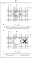
- FIG. 2A is a plan view for explaining the relationship between the imaging holes 6 formed in the display panel 2 of the EL device 1 and the scanning signal lines 10 and the data signal lines 11, and FIG. It is sectional drawing, (c) is a top view for demonstrating the relationship between the imaging hole 96 which concerns on a comparative example, the scanning signal line 10, and the data signal line 11, (d) is the sectional view. .
- the display panel 2 includes a panel substrate 4 on which a plurality of scanning signal lines 10 and a plurality of data signal lines 11 crossing the plurality of scanning signal lines 10 are formed, and a plurality of scanning signals from the plurality of scanning signal lines 10 And an EL layer 5 formed on the panel substrate 4 in order to display an image based on the data signal from the data signal line 11 of FIG.
- the sealing layer 14 is formed on the EL layer 5.
- FIG. 3 is a plan view for explaining the relationship between the imaging hole 6 formed in the display panel 2 and the transistor 21.
- FIG. 4A is a cross-sectional view of the EL device in the area where the imaging hole 6 is not formed
- FIG. 4B is a cross-sectional view of the EL device in the area where the imaging hole 6 is formed.
- An imaging hole 6 for guiding light Lx from a subject to the imaging element 3 straddles the plurality of scanning signal lines 10 and the plurality of data signal lines 11 when viewed from the direction perpendicular to the display surface 7 of the display panel 2 It is formed in the display area 8.
- the plurality of scanning signal lines 10 and the plurality of data signal lines 11 are made of a transparent material. This is because the light Lx from the subject is favorably transmitted through the scanning signal line 10 and the data signal line 11 and is incident on the imaging device 3.
- the transistor layer 12 formed between the panel substrate 4 and the EL layer 5 is a plurality of transistors formed in the plurality of pixels 22 corresponding to the respective intersections of the plurality of scanning signal lines 10 and the plurality of data signal lines 11. It has 21.
- the transistor 21 of the transistor layer 12 is not formed in the region corresponding to the imaging hole 6 as shown in FIG. 3 and FIG. 4B, and only the plurality of scanning signal lines 10 and the plurality of data signal lines 11 It is formed in a region corresponding to the imaging hole 6 between the substrate 4 and the EL layer 5.
- the area of the pixel 22 in which the transistor 21 is formed is lit by the EL layer 5, but the area of the pixel 22 inside the imaging hole 6 in which the transistor 21 is not formed is not lit even if the EL layer 5 is formed.
- the transistor 21 is not formed with the pixel 22 whose half or more part is inside the imaging hole 6 as a “non-lighting pixel”.
- the transistor 21 may not be formed as a pixel which is partially unlit inside the imaging hole 6 as a "non-lighting pixel”.
- the transistor 21 of the transistor layer 12 is formed in the region excluding the imaging hole 6.
- An optical sheet 17 such as a polarizing plate is formed on the protective film 16.
- the optical sheet 17 is formed in the area where the imaging hole 6 is not formed, and is not formed in the area corresponding to the imaging hole 6.
- the protective film 16 is also formed in the area corresponding to the imaging hole 6, but preferably has high transparency.
- the EL layer 5 is also formed in a region corresponding to the imaging hole 6.
- the panel substrate 4 is also formed in the area corresponding to the imaging hole 6, but preferably has high transparency.
- the scanning signal line 10 and the data signal line 11 intersecting the imaging hole 96 are divided by the imaging hole 96 Break. Therefore, the scanning signal can not be transmitted through the scanning signal line 10, and the data signal can not be transmitted through the data signal line 11. Accordingly, there arises a problem that a good image can not be displayed on the display area 8 of the display panel 2.
- the imaging holes 6 corresponding to the imaging element 3 are formed in the display area 8 so as to straddle the plurality of scanning signal lines 10 and the plurality of data signal lines 11. Therefore, the imaging holes 6 with a large aperture diameter can be formed in the display area 8 of the display panel 2 while maintaining the plurality of scanning signal lines 10 and the plurality of data signal lines 11 as they are. Therefore, the camera can be mounted in the display area 8 of the display panel 2.
- FIG. 5A is a cross-sectional view of the EL device in the area where the imaging hole 6 is not formed
- FIG. 5B is an EL in the area where the imaging hole 6 formed in the display panel of the EL device according to the second embodiment is formed
- FIG. 2 is a cross-sectional view of the device.
- the EL layer 5 is formed in the first embodiment.
- the EL layer 5 is also formed in the region corresponding to the imaging hole 6.
- the EL layer 5 is formed in the area where the imaging hole 6 is not formed, and is not formed in the area corresponding to the imaging hole 6.
- the EL layer 5 does not exist in the imaging hole 6. Therefore, the light Lx traveling from the subject toward the imaging device 3 through the imaging hole 6 is more favorably incident on the imaging device 3.
- the EL device includes a display panel for displaying an image in a display area in a display surface, and an imaging device disposed on the surface opposite to the display surface to capture an object on the display surface.
- a panel substrate having a plurality of scanning signal lines and a plurality of data signal lines crossing the plurality of scanning signal lines, and a scanning signal from the plurality of scanning signal lines, And an EL layer formed on the panel substrate to display the image based on data signals from the plurality of data signal lines, and to guide light from the subject to the imaging device.
- An imaging hole is formed in the display area so as to straddle the plurality of scanning signal lines and the plurality of data signal lines when viewed in a direction perpendicular to the display surface.
- the plurality of scanning signal lines and the plurality of data signal lines are made of a transparent material, and light from the subject is transmitted through the scanning signal line and the data signal line to be incident on the imaging device. .
- the panel substrate includes a transistor, and the transistor is formed in a region of the panel substrate excluding the imaging hole.
- the EL layer is formed in an area excluding the imaging hole.
- the EL layer is formed in a region including the imaging hole.
- an imaging element arranging step of arranging an imaging element on the surface side of the display panel wherein the display panel forming step includes a plurality of scanning signal lines and a plurality of data signal lines intersecting the plurality of scanning signal lines.
- a manufacturing apparatus of an EL device includes a display panel forming mechanism for forming a display panel for displaying an image in a display area in the display surface, and an opposite side to the display surface for capturing an object on the display surface. And an image pickup device arranging mechanism for arranging an image pickup device on the surface side of the display panel, and the display panel forming mechanism is formed with a plurality of scanning signal lines and a plurality of data signal lines intersecting the plurality of scanning signal lines.
- a panel substrate manufacturing mechanism for manufacturing a panel substrate, an EL layer for displaying the image based on scanning signals from the plurality of scanning signal lines, and data signals from the plurality of data signal lines;
- the plurality of scanning signal lines and the plurality of scanning signal lines and the plurality of scanning signal lines are viewed from a direction perpendicular to the display surface, and an EL layer formation mechanism formed on a substrate and an imaging hole for guiding light from the subject to the imaging device.
- data And an imaging hole forming mechanism that forms Route in the display area so as to straddle the.
Landscapes
- Engineering & Computer Science (AREA)
- Microelectronics & Electronic Packaging (AREA)
- Physics & Mathematics (AREA)
- Multimedia (AREA)
- Chemical & Material Sciences (AREA)
- Inorganic Chemistry (AREA)
- Signal Processing (AREA)
- Geometry (AREA)
- Devices For Indicating Variable Information By Combining Individual Elements (AREA)
- Life Sciences & Earth Sciences (AREA)
- Sustainable Development (AREA)
- Theoretical Computer Science (AREA)
- General Physics & Mathematics (AREA)
- Manufacturing & Machinery (AREA)
- Electroluminescent Light Sources (AREA)
- Studio Devices (AREA)
Abstract
ELデバイス(1)が、表示パネル(2)と撮像素子(3)とを備え、表示パネル(2)がパネル基板(4)とEL層(5)とを有し、被写体からの光を撮像素子(3)に導くための撮像孔(6)が、表示面に垂直な方向から見て、複数の走査信号線(10)及び複数のデータ信号線(11)を跨ぐように表示エリア(8)に形成される。
Description
本発明は、被写体からの光を撮像素子に導くための撮像孔が表示パネルに形成されたEL(Electro Luminescence:エレクトロルミネッセンス)デバイス、ELデバイスの製造方法、及びELデバイスの製造装置に関する。
全面表示の表示パネルにカメラを搭載するために、表示パネルの表示面の有効領域に、撮像素子に対応する大開口径の撮像孔を形成する構成が知られている(特許文献1)。
しかしながら、表示パネルの表示面の有効領域に大開口径の撮像孔を形成すると、表示パネルのパネル基板に形成された複数の走査信号線と複数のデータ信号線とを貫通して撮像孔が形成される。このため、複数の走査信号線と複数のデータ信号線とが分断されて断線してしまうという問題が生じる。
本発明の一態様は、複数の走査信号線と複数のデータ信号線とをそのままに維持しながら撮像孔を表示パネルの有効領域に形成することができるELデバイス、ELデバイスの製造方法、及びELデバイスの製造装置を実現することにある。
本発明の一態様に係るELデバイスは、表示面内の表示エリアに画像を表示する表示パネルと、前記表示面側の被写体を撮像するために、前記表示面と反対側の面側に配置された撮像素子とを備え、前記表示パネルが、複数の走査信号線と、前記複数の走査信号線に交差する複数のデータ信号線とが形成されたパネル基板と、前記複数の走査信号線からの走査信号と、前記複数のデータ信号線からのデータ信号とに基づいて前記画像を表示するために、前記パネル基板の上に形成されたEL層とを有し、前記被写体からの光を前記撮像素子に導くための撮像孔が、前記表示面に垂直な方向から見て、前記複数の走査信号線及び前記複数のデータ信号線を跨ぐように前記表示エリアに形成されることを特徴とする。
本発明の一態様によれば、複数の走査信号線と複数のデータ信号線とをそのままに維持しながら撮像孔を表示パネルの有効領域に形成することができる。
(実施形態1)
図1(a)は実施形態1に係るELデバイス1の平面図であり、(b)は(a)に示される面AAに沿った断面図である。ELデバイス1は表示パネル2を備える。表示パネル2の表示面7には、画像を表示するための表示エリア8と、表示エリア8を囲むように設けられた額縁状の非表示エリア13とが配置される。表示パネル2の上には保護膜16が接着層15を介して設けられる。そして、保護膜16の上に光学シート17が設けられる(図4)。
図1(a)は実施形態1に係るELデバイス1の平面図であり、(b)は(a)に示される面AAに沿った断面図である。ELデバイス1は表示パネル2を備える。表示パネル2の表示面7には、画像を表示するための表示エリア8と、表示エリア8を囲むように設けられた額縁状の非表示エリア13とが配置される。表示パネル2の上には保護膜16が接着層15を介して設けられる。そして、保護膜16の上に光学シート17が設けられる(図4)。
ELデバイス1には、表示パネル2の表示面7側に存在する図示しない被写体を撮像するために、表示面7と反対の面側に配置された撮像素子3が設けられる。
図2(a)はELデバイス1の表示パネル2に形成された撮像孔6と走査信号線10及びデータ信号線11との間の関係を説明するための平面図であり、(b)はその断面図であり、(c)は比較例に係る撮像孔96と走査信号線10及びデータ信号線11との間の関係を説明するための平面図であり、(d)はその断面図である。
表示パネル2は、複数の走査信号線10と、複数の走査信号線10に交差する複数のデータ信号線11とが形成されたパネル基板4と、複数の走査信号線10からの走査信号と複数のデータ信号線11からのデータ信号とに基づいて画像を表示するために、パネル基板4の上に形成されたEL層5とを有する。表示パネル2には、EL層5の上に封止層14が形成される。
図3は表示パネル2に形成された撮像孔6とトランジスタ21との間の関係を説明するための平面図である。図4(a)は撮像孔6が形成されない領域におけるELデバイスの断面図であり、(b)は撮像孔6が形成される領域におけるELデバイスの断面図である。
被写体からの光Lxを撮像素子3に導くための撮像孔6が、表示パネル2の表示面7に垂直な方向から見て、複数の走査信号線10及び複数のデータ信号線11を跨ぐように表示エリア8内に形成される。
複数の走査信号線10及び複数のデータ信号線11が透明な材料で構成されることが好ましい。被写体からの光Lxが走査信号線10及びデータ信号線11を良好に透過して撮像素子3に入射するためである。
パネル基板4とEL層5との間に形成されるトランジスタ層12は、複数の走査信号線10及び複数のデータ信号線11のそれぞれの交点に対応する複数の画素22に形成される複数のトランジスタ21を有する。トランジスタ層12のトランジスタ21は、図3及び図4(b)に示すように、撮像孔6に相当する領域には形成されず、複数の走査信号線10及び複数のデータ信号線11のみがパネル基板4とEL層5との間の撮像孔6に相当する領域に形成される。
従って、トランジスタ21が形成される画素22の領域はEL層5により点灯するが、トランジスタ21が形成されない撮像孔6の内側の画素22の領域はEL層5が形成されていても点灯しない。
例えば図3に示すように、半分以上の部分が撮像孔6の内側に入っている画素22を「点灯しない画素」としてトランジスタ21を形成しないように構成することができる。撮像孔6の内側に一部でも入っている画素22を「点灯しない画素」としてトランジスタ21を形成しないように構成してもよい。このように、トランジスタ層12のトランジスタ21は、撮像孔6を除く領域に形成される。
保護膜16の上に偏光板等の光学シート17が形成される。この光学シート17は、撮像孔6が形成されない領域に形成され、撮像孔6に相当する領域には形成されない。
保護膜16は、撮像孔6に相当する領域にも形成されるが、高い透明度を有していることが好ましい。
EL層5は撮像孔6に相当する領域にも形成される。
パネル基板4は、撮像孔6に相当する領域にも形成されるが、高い透明度を有していることが好ましい。
図2(b)に示すように、撮像素子3に対応する撮像孔96として、単純な貫通孔を形成すると、撮像孔96に交わる走査信号線10及びデータ信号線11が撮像孔96により分断されて断線する。このため、走査信号を走査信号線10により伝達することができず、データ信号をデータ信号線11により伝達することができなくなる。従って、表示パネル2の表示エリア8に良好な画像を表示することができなくなるという問題が生じる。
これに対して本実施の形態では、撮像素子3に対応する撮像孔6が、複数の走査信号線10及び複数のデータ信号線11を跨ぐように表示エリア8に形成される。このため、複数の走査信号線10と複数のデータ信号線11とをそのままに維持しながら大開口径の撮像孔6を表示パネル2の表示エリア8内に形成することができる。従って、表示パネル2の表示エリア8内にカメラを搭載することができる。
(実施形態2)
本発明の他の実施形態について、以下に説明する。なお、説明の便宜上、上記実施形態にて説明した部材と同じ機能を有する部材については、同じ符号を付記し、その説明を省略する。
本発明の他の実施形態について、以下に説明する。なお、説明の便宜上、上記実施形態にて説明した部材と同じ機能を有する部材については、同じ符号を付記し、その説明を省略する。
図5(a)は撮像孔6が形成されない領域におけるELデバイスの断面図であり、(b)は実施形態2に係るELデバイスの表示パネルに形成された撮像孔6が形成される領域におけるELデバイスの断面図である。
前述した実施形態1と異なる点は、EL層5の形成される領域である。実施形態1では、EL層5は撮像孔6に相当する領域にも形成された。これに対して実施形態2では、図5(b)に示すように、EL層5は、撮像孔6が形成されない領域に形成され、撮像孔6に相当する領域には形成されない。
これにより、EL層5が撮像孔6に存在しなくなる。このため、被写体から撮像孔6を通って撮像素子3に向かう光Lxがより良好に撮像素子3に入射する。
〔まとめ〕
態様1のELデバイスは、表示面内の表示エリアに画像を表示する表示パネルと、前記表示面側の被写体を撮像するために、前記表示面と反対側の面側に配置された撮像素子とを備え、前記表示パネルが、複数の走査信号線と、前記複数の走査信号線に交差する複数のデータ信号線とが形成されたパネル基板と、前記複数の走査信号線からの走査信号と、前記複数のデータ信号線からのデータ信号とに基づいて前記画像を表示するために、前記パネル基板の上に形成されたEL層とを有し、前記被写体からの光を前記撮像素子に導くための撮像孔が、前記表示面に垂直な方向から見て、前記複数の走査信号線及び前記複数のデータ信号線を跨ぐように前記表示エリアに形成される。
態様1のELデバイスは、表示面内の表示エリアに画像を表示する表示パネルと、前記表示面側の被写体を撮像するために、前記表示面と反対側の面側に配置された撮像素子とを備え、前記表示パネルが、複数の走査信号線と、前記複数の走査信号線に交差する複数のデータ信号線とが形成されたパネル基板と、前記複数の走査信号線からの走査信号と、前記複数のデータ信号線からのデータ信号とに基づいて前記画像を表示するために、前記パネル基板の上に形成されたEL層とを有し、前記被写体からの光を前記撮像素子に導くための撮像孔が、前記表示面に垂直な方向から見て、前記複数の走査信号線及び前記複数のデータ信号線を跨ぐように前記表示エリアに形成される。
態様2では、前記複数の走査信号線及び前記複数のデータ信号線が透明な材料で構成され、前記被写体からの光が前記走査信号線及び前記データ信号線を透過して前記撮像素子に入射する。
態様3では、前記パネル基板がトランジスタを有し、前記トランジスタが、前記パネル基板の前記撮像孔を除く領域に形成される。
態様4では、前記EL層が前記撮像孔を除く領域に形成される。
態様5では、前記EL層が前記撮像孔を含む領域に形成される。
態様6のELデバイスの製造方法は、表示面内の表示エリアに画像を表示する表示パネルを形成する表示パネル形成工程と、前記表示面側の被写体を撮像するために、前記表示面と反対側の面側に撮像素子を配置する撮像素子配置工程とを包含し、前記表示パネル形成工程が、複数の走査信号線と、前記複数の走査信号線に交差する複数のデータ信号線とが形成されたパネル基板を製造するパネル基板製造工程と、前記複数の走査信号線からの走査信号と、前記複数のデータ信号線からのデータ信号とに基づいて前記画像を表示するためのEL層を、前記パネル基板の上に形成するEL層形成工程と、前記被写体からの光を前記撮像素子に導くための撮像孔を、前記表示面に垂直な方向から見て、前記複数の走査信号線及び前記複数のデータ信号線を跨ぐように前記表示エリアに形成する撮像孔形成工程とを含む。
態様7のELデバイスの製造装置は、表示面内の表示エリアに画像を表示する表示パネルを形成する表示パネル形成機構と、前記表示面側の被写体を撮像するために、前記表示面と反対側の面側に撮像素子を配置する撮像素子配置機構とを備え、前記表示パネル形成機構が、複数の走査信号線と、前記複数の走査信号線に交差する複数のデータ信号線とが形成されたパネル基板を製造するパネル基板製造機構と、前記複数の走査信号線からの走査信号と、前記複数のデータ信号線からのデータ信号とに基づいて前記画像を表示するためのEL層を、前記パネル基板の上に形成するEL層形成機構と、前記被写体からの光を前記撮像素子に導くための撮像孔を、前記表示面に垂直な方向から見て、前記複数の走査信号線及び前記複数のデータ信号線を跨ぐように前記表示エリアに形成する撮像孔形成機構とを有する。
本発明は上述した各実施形態に限定されるものではなく、請求項に示した範囲で種々の変更が可能であり、異なる実施形態にそれぞれ開示された技術的手段を適宜組み合わせて得られる実施形態についても本発明の技術的範囲に含まれる。さらに、各実施形態にそれぞれ開示された技術的手段を組み合わせることにより、新しい技術的特徴を形成することができる。
1 ELデバイス
2 表示パネル
3 撮像素子
4 パネル基板
5 EL層
6 撮像孔
7 表示面
8 表示エリア
10 走査信号線
11 データ信号線
12 トランジスタ層
21 トランジスタ
2 表示パネル
3 撮像素子
4 パネル基板
5 EL層
6 撮像孔
7 表示面
8 表示エリア
10 走査信号線
11 データ信号線
12 トランジスタ層
21 トランジスタ
Claims (7)
- 表示面内の表示エリアに画像を表示する表示パネルと、
前記表示面側の被写体を撮像するために、前記表示面と反対側の面側に配置された撮像素子とを備え、
前記表示パネルが、複数の走査信号線と、前記複数の走査信号線に交差する複数のデータ信号線とが形成されたパネル基板と、
前記複数の走査信号線からの走査信号と、前記複数のデータ信号線からのデータ信号とに基づいて前記画像を表示するために、前記パネル基板の上に形成されたEL層とを有し、
前記被写体からの光を前記撮像素子に導くための撮像孔が、前記表示面に垂直な方向から見て、前記複数の走査信号線及び前記複数のデータ信号線を跨ぐように前記表示エリアに形成されることを特徴とするELデバイス。 - 前記複数の走査信号線及び前記複数のデータ信号線が透明な材料で構成され、
前記被写体からの光が前記走査信号線及び前記データ信号線を透過して前記撮像素子に入射する請求項1に記載のELデバイス。 - 前記パネル基板がトランジスタを有し、
前記トランジスタが、前記パネル基板の前記撮像孔を除く領域に形成される請求項1に記載のELデバイス。 - 前記EL層が前記撮像孔を除く領域に形成される請求項1に記載のELデバイス。
- 前記EL層が前記撮像孔を含む領域に形成される請求項1に記載のELデバイス。
- 表示面内の表示エリアに画像を表示する表示パネルを形成する表示パネル形成工程と、
前記表示面側の被写体を撮像するために、前記表示面と反対側の面側に撮像素子を配置する撮像素子配置工程とを包含し、
前記表示パネル形成工程が、複数の走査信号線と、前記複数の走査信号線に交差する複数のデータ信号線とが形成されたパネル基板を製造するパネル基板製造工程と、
前記複数の走査信号線からの走査信号と、前記複数のデータ信号線からのデータ信号とに基づいて前記画像を表示するためのEL層を、前記パネル基板の上に形成するEL層形成工程と、
前記被写体からの光を前記撮像素子に導くための撮像孔を、前記表示面に垂直な方向から見て、前記複数の走査信号線及び前記複数のデータ信号線を跨ぐように前記表示エリアに形成する撮像孔形成工程とを含むことを特徴とするELデバイスの製造方法。 - 表示面内の表示エリアに画像を表示する表示パネルを形成する表示パネル形成機構と、
前記表示面側の被写体を撮像するために、前記表示面と反対側の面側に撮像素子を配置する撮像素子配置機構とを備え、
前記表示パネル形成機構が、複数の走査信号線と、前記複数の走査信号線に交差する複数のデータ信号線とが形成されたパネル基板を製造するパネル基板製造機構と、
前記複数の走査信号線からの走査信号と、前記複数のデータ信号線からのデータ信号とに基づいて前記画像を表示するためのEL層を、前記パネル基板の上に形成するEL層形成機構と、
前記被写体からの光を前記撮像素子に導くための撮像孔を、前記表示面に垂直な方向から見て、前記複数の走査信号線及び前記複数のデータ信号線を跨ぐように前記表示エリアに形成する撮像孔形成機構とを有することを特徴とするELデバイスの製造装置。
Priority Applications (4)
| Application Number | Priority Date | Filing Date | Title |
|---|---|---|---|
| CN201780092396.9A CN110809907B (zh) | 2017-07-10 | 2017-07-10 | El设备、el设备的制造方法及el设备的制造装置 |
| US16/466,686 US10770522B2 (en) | 2017-07-10 | 2017-07-10 | EL device, manufacturing method for EL device, and manufacturing apparatus for EL device |
| PCT/JP2017/025151 WO2019012583A1 (ja) | 2017-07-10 | 2017-07-10 | Elデバイス、elデバイスの製造方法、及びelデバイスの製造装置 |
| JP2019529336A JP6723456B2 (ja) | 2017-07-10 | 2017-07-10 | Elデバイス、elデバイスの製造方法、及びelデバイスの製造装置 |
Applications Claiming Priority (1)
| Application Number | Priority Date | Filing Date | Title |
|---|---|---|---|
| PCT/JP2017/025151 WO2019012583A1 (ja) | 2017-07-10 | 2017-07-10 | Elデバイス、elデバイスの製造方法、及びelデバイスの製造装置 |
Publications (1)
| Publication Number | Publication Date |
|---|---|
| WO2019012583A1 true WO2019012583A1 (ja) | 2019-01-17 |
Family
ID=65001851
Family Applications (1)
| Application Number | Title | Priority Date | Filing Date |
|---|---|---|---|
| PCT/JP2017/025151 Ceased WO2019012583A1 (ja) | 2017-07-10 | 2017-07-10 | Elデバイス、elデバイスの製造方法、及びelデバイスの製造装置 |
Country Status (4)
| Country | Link |
|---|---|
| US (1) | US10770522B2 (ja) |
| JP (1) | JP6723456B2 (ja) |
| CN (1) | CN110809907B (ja) |
| WO (1) | WO2019012583A1 (ja) |
Cited By (2)
| Publication number | Priority date | Publication date | Assignee | Title |
|---|---|---|---|---|
| CN110890026A (zh) * | 2019-12-05 | 2020-03-17 | 昆山国显光电有限公司 | 显示面板及显示装置 |
| WO2020191850A1 (zh) * | 2019-03-28 | 2020-10-01 | 武汉华星光电半导体显示技术有限公司 | 显示面板以及显示装置 |
Families Citing this family (4)
| Publication number | Priority date | Publication date | Assignee | Title |
|---|---|---|---|---|
| TWI636446B (zh) * | 2017-11-08 | 2018-09-21 | 友達光電股份有限公司 | 顯示面板 |
| TWI690912B (zh) * | 2019-02-13 | 2020-04-11 | 友達光電股份有限公司 | 顯示面板及驅動方法 |
| CN112462545B (zh) | 2020-12-02 | 2025-03-21 | 武汉天马微电子有限公司 | 显示面板及显示装置 |
| KR20220168639A (ko) | 2021-06-16 | 2022-12-26 | 삼성디스플레이 주식회사 | 표시장치, 전자장치 및 표시장치 제조방법 |
Citations (6)
| Publication number | Priority date | Publication date | Assignee | Title |
|---|---|---|---|---|
| JP2011120200A (ja) * | 2009-11-02 | 2011-06-16 | Sony Corp | 撮像装置付き画像表示装置 |
| WO2012164259A1 (en) * | 2011-05-27 | 2012-12-06 | Cambridge Enterprise Limited | Electronic devices |
| JP2014067577A (ja) * | 2012-09-26 | 2014-04-17 | Seiko Epson Corp | 撮像装置 |
| JP2015005280A (ja) * | 2013-05-20 | 2015-01-08 | 株式会社半導体エネルギー研究所 | 撮像パネル、撮像装置 |
| JP2016029794A (ja) * | 2014-07-18 | 2016-03-03 | 株式会社半導体エネルギー研究所 | 表示システム、撮像装置、監視装置、表示装置、及び電子機器 |
| JP2017097342A (ja) * | 2015-11-13 | 2017-06-01 | 株式会社半導体エネルギー研究所 | 表示装置、入出力装置、情報処理装置 |
Family Cites Families (14)
| Publication number | Priority date | Publication date | Assignee | Title |
|---|---|---|---|---|
| US6747290B2 (en) * | 2000-12-12 | 2004-06-08 | Semiconductor Energy Laboratory Co., Ltd. | Information device |
| JP3980462B2 (ja) * | 2002-10-30 | 2007-09-26 | 株式会社 日立ディスプレイズ | 画像表示装置 |
| JP4886162B2 (ja) | 2003-06-18 | 2012-02-29 | キヤノン株式会社 | 撮像装置付き表示装置 |
| JP4759511B2 (ja) * | 2004-04-19 | 2011-08-31 | 株式会社日立製作所 | 撮像機能一体型表示装置 |
| JP4518199B2 (ja) * | 2007-10-23 | 2010-08-04 | エプソンイメージングデバイス株式会社 | 電気光学装置 |
| JP2010230797A (ja) | 2009-03-26 | 2010-10-14 | Seiko Epson Corp | 表示装置、および電子機器 |
| JP5442754B2 (ja) * | 2009-10-28 | 2014-03-12 | シャープ株式会社 | アクティブマトリクス基板、液晶パネル、液晶表示装置、液晶表示ユニット、テレビジョン受像機 |
| US8502756B2 (en) * | 2009-11-02 | 2013-08-06 | Sony Corporation | Image display device with imaging unit |
| KR102418520B1 (ko) * | 2015-09-04 | 2022-07-08 | 삼성디스플레이 주식회사 | 표시 장치 |
| KR102465379B1 (ko) * | 2015-12-02 | 2022-11-10 | 삼성디스플레이 주식회사 | 디스플레이 장치 |
| WO2017147614A1 (en) * | 2016-02-26 | 2017-08-31 | Essential Products, Inc. | Image capture with a camera integrated display |
| CN107425038B (zh) * | 2017-06-09 | 2020-01-21 | 武汉天马微电子有限公司 | 一种有机发光显示面板及其制造方法、以及电子设备 |
| CN108922905A (zh) * | 2018-07-17 | 2018-11-30 | 京东方科技集团股份有限公司 | 一种显示基板及制备方法、显示面板 |
| US10707281B2 (en) * | 2018-08-10 | 2020-07-07 | Au Optronics Corporation | Display apparatus |
-
2017
- 2017-07-10 JP JP2019529336A patent/JP6723456B2/ja active Active
- 2017-07-10 US US16/466,686 patent/US10770522B2/en active Active
- 2017-07-10 WO PCT/JP2017/025151 patent/WO2019012583A1/ja not_active Ceased
- 2017-07-10 CN CN201780092396.9A patent/CN110809907B/zh active Active
Patent Citations (6)
| Publication number | Priority date | Publication date | Assignee | Title |
|---|---|---|---|---|
| JP2011120200A (ja) * | 2009-11-02 | 2011-06-16 | Sony Corp | 撮像装置付き画像表示装置 |
| WO2012164259A1 (en) * | 2011-05-27 | 2012-12-06 | Cambridge Enterprise Limited | Electronic devices |
| JP2014067577A (ja) * | 2012-09-26 | 2014-04-17 | Seiko Epson Corp | 撮像装置 |
| JP2015005280A (ja) * | 2013-05-20 | 2015-01-08 | 株式会社半導体エネルギー研究所 | 撮像パネル、撮像装置 |
| JP2016029794A (ja) * | 2014-07-18 | 2016-03-03 | 株式会社半導体エネルギー研究所 | 表示システム、撮像装置、監視装置、表示装置、及び電子機器 |
| JP2017097342A (ja) * | 2015-11-13 | 2017-06-01 | 株式会社半導体エネルギー研究所 | 表示装置、入出力装置、情報処理装置 |
Cited By (2)
| Publication number | Priority date | Publication date | Assignee | Title |
|---|---|---|---|---|
| WO2020191850A1 (zh) * | 2019-03-28 | 2020-10-01 | 武汉华星光电半导体显示技术有限公司 | 显示面板以及显示装置 |
| CN110890026A (zh) * | 2019-12-05 | 2020-03-17 | 昆山国显光电有限公司 | 显示面板及显示装置 |
Also Published As
| Publication number | Publication date |
|---|---|
| CN110809907B (zh) | 2022-05-10 |
| CN110809907A (zh) | 2020-02-18 |
| JP6723456B2 (ja) | 2020-07-15 |
| US10770522B2 (en) | 2020-09-08 |
| US20190363141A1 (en) | 2019-11-28 |
| JPWO2019012583A1 (ja) | 2020-04-23 |
Similar Documents
| Publication | Publication Date | Title |
|---|---|---|
| WO2019012583A1 (ja) | Elデバイス、elデバイスの製造方法、及びelデバイスの製造装置 | |
| US10599190B2 (en) | Image display device including a camera and being able to prevent an image pickup window part from reducing a display area | |
| KR101511117B1 (ko) | 양면 디스플레이장치 | |
| CN108153071B (zh) | 显示面板及其制造方法、显示装置 | |
| TWI611385B (zh) | 雙面顯示裝置及其製造方法 | |
| TWI662344B (zh) | 電子機器及顯示裝置之製造方法 | |
| US9772437B2 (en) | Display, display assembly, and backlight module | |
| US10916187B2 (en) | Display apparatus | |
| WO2016041272A1 (zh) | 阵列基板及其显示装置 | |
| EP2071435A3 (en) | Display device and method for manufacturing the same | |
| KR102159747B1 (ko) | 표시장치 | |
| CN113841194B (zh) | 显示装置以及显示面板 | |
| CN102998865A (zh) | 一种阵列基板及其制作方法、显示装置 | |
| CN104635395A (zh) | 一种平板显示装置 | |
| CN107831612A (zh) | 显示面板、显示装置以及显示方法 | |
| US20210037639A1 (en) | Display apparatus | |
| WO2016165282A1 (zh) | 阵列基板、显示面板及显示装置 | |
| JP6328794B2 (ja) | 表示装置及び表示装置の製造方法 | |
| JP6287252B2 (ja) | 電気光学装置及び電子機器 | |
| CN104865744A (zh) | 一种3d显示装置及其制作方法 | |
| KR102674786B1 (ko) | 멀티스크린 표시장치 및 이의 제조방법 | |
| US20110317262A1 (en) | Optical Film and Stereoscopic Display Using the Same | |
| JP2014167582A (ja) | 表示装置 | |
| CN105807522A (zh) | 阵列基板及其制作方法、显示面板 | |
| JP2014022060A (ja) | バックライト装置、表示装置、及びテレビ受信装置 |
Legal Events
| Date | Code | Title | Description |
|---|---|---|---|
| 121 | Ep: the epo has been informed by wipo that ep was designated in this application |
Ref document number: 17917733 Country of ref document: EP Kind code of ref document: A1 |
|
| ENP | Entry into the national phase |
Ref document number: 2019529336 Country of ref document: JP Kind code of ref document: A |
|
| NENP | Non-entry into the national phase |
Ref country code: DE |
|
| 122 | Ep: pct application non-entry in european phase |
Ref document number: 17917733 Country of ref document: EP Kind code of ref document: A1 |