WO2019004484A1 - 磁気ディスク用基板及び磁気ディスク - Google Patents
磁気ディスク用基板及び磁気ディスク Download PDFInfo
- Publication number
- WO2019004484A1 WO2019004484A1 PCT/JP2018/025104 JP2018025104W WO2019004484A1 WO 2019004484 A1 WO2019004484 A1 WO 2019004484A1 JP 2018025104 W JP2018025104 W JP 2018025104W WO 2019004484 A1 WO2019004484 A1 WO 2019004484A1
- Authority
- WO
- WIPO (PCT)
- Prior art keywords
- substrate
- film
- magnetic disk
- thickness
- main surface
- Prior art date
- Legal status (The legal status is an assumption and is not a legal conclusion. Google has not performed a legal analysis and makes no representation as to the accuracy of the status listed.)
- Ceased
Links
Images


Classifications
-
- G—PHYSICS
- G11—INFORMATION STORAGE
- G11B—INFORMATION STORAGE BASED ON RELATIVE MOVEMENT BETWEEN RECORD CARRIER AND TRANSDUCER
- G11B5/00—Recording by magnetisation or demagnetisation of a record carrier; Reproducing by magnetic means; Record carriers therefor
- G11B5/62—Record carriers characterised by the selection of the material
- G11B5/73—Base layers, i.e. all non-magnetic layers lying under a lowermost magnetic recording layer, e.g. including any non-magnetic layer in between a first magnetic recording layer and either an underlying substrate or a soft magnetic underlayer
- G11B5/739—Magnetic recording media substrates
- G11B5/73911—Inorganic substrates
- G11B5/73921—Glass or ceramic substrates
-
- G—PHYSICS
- G11—INFORMATION STORAGE
- G11B—INFORMATION STORAGE BASED ON RELATIVE MOVEMENT BETWEEN RECORD CARRIER AND TRANSDUCER
- G11B5/00—Recording by magnetisation or demagnetisation of a record carrier; Reproducing by magnetic means; Record carriers therefor
- G11B5/62—Record carriers characterised by the selection of the material
- G11B5/73—Base layers, i.e. all non-magnetic layers lying under a lowermost magnetic recording layer, e.g. including any non-magnetic layer in between a first magnetic recording layer and either an underlying substrate or a soft magnetic underlayer
- G11B5/739—Magnetic recording media substrates
- G11B5/73911—Inorganic substrates
- G11B5/73913—Composites or coated substrates
-
- G—PHYSICS
- G11—INFORMATION STORAGE
- G11B—INFORMATION STORAGE BASED ON RELATIVE MOVEMENT BETWEEN RECORD CARRIER AND TRANSDUCER
- G11B5/00—Recording by magnetisation or demagnetisation of a record carrier; Reproducing by magnetic means; Record carriers therefor
- G11B5/62—Record carriers characterised by the selection of the material
- G11B5/73—Base layers, i.e. all non-magnetic layers lying under a lowermost magnetic recording layer, e.g. including any non-magnetic layer in between a first magnetic recording layer and either an underlying substrate or a soft magnetic underlayer
- G11B5/739—Magnetic recording media substrates
- G11B5/73911—Inorganic substrates
- G11B5/73917—Metallic substrates, i.e. elemental metal or metal alloy substrates
- G11B5/73919—Aluminium or titanium elemental or alloy substrates
Definitions
- the present invention relates to a magnetic disk substrate and a magnetic disk.
- a magnetic disk substrate Conventionally, glass substrates and aluminum alloy substrates have been used as magnetic disk substrates. On these substrates, a magnetic film is formed on the main surface of the substrate to form a magnetic disk. It is desirable that a magnetic disk has few surface defects, has no problem in reading and writing information, and can read and write a large amount of information.
- NiP plating is performed on the surface of the aluminum alloy substrate.
- metal film is formed on the substrate surface by physical vapor deposition.
- Al alloy substrate for a magnetic recording medium in which an Al.
- the Al alloy substrate for a magnetic recording medium is said to be capable of reducing surface defects after NiP plating formed on the substrate. This can provide a magnetic disk capable of reading and writing a large amount of information without any problem in reading and writing information.
- HDDs hard disk drives
- the vibration generated by the external impact decays with time, unlike the steady state flutter vibration generated in the steady state of rotation caused by the flow of the rotating magnetic disk and the air around it.
- the magnetic head contacts the ramp member provided to project on the main surface of the magnetic disk to retract from the magnetic disk, and the ramp member is scraped, etc.
- scratches and defects occur on the surface of the magnetic disk.
- contact occurs repeatedly at the same position on the magnetic disk when the magnetic disk is not rotating, particles on the surface of the magnetic disk, Scratches and defects are even more likely to occur.
- the thickness of a nominal 3.5 inch magnetic disk substrate is as thick as 0.8 mm or more, so that an amplitude which causes a problem due to external impact is unlikely to occur.
- the distance (gap) between the magnetic disk and the lamp is relatively large. For this reason, the magnetic disk and the lamp hardly come in contact with each other.
- the thickness of the magnetic disk substrate is reduced to increase the storage capacity of the hard disk drive, etc., the vibration due to the external impact, which has not caused any problems in the prior art, and the lamp member etc. It has become impossible to ignore contact with other members, as well as particles and scratches and dents of the magnetic disk that occur as a result of the contact.
- the present invention can effectively reduce the number of times the magnetic disk contacts the external member due to the vibration of the magnetic disk different from the flutter vibration generated by the impact received from the outside even when the thickness of the substrate is reduced. It is an object of the present invention to provide a magnetic disk substrate and a magnetic disk that can be used.
- the substrate is A substrate body having two major surfaces; And a film of a metallic material provided with the main surface and having a loss factor value of 0.01 or more.
- the thickness T of the magnetic disk substrate including the film is 0.700 mm or less.
- the thickness D [mm] of the film provided on the main surface and the thickness T [mm] of the substrate including the film satisfy the following formula (1). D 0.00 0.0082 / T-0.0015 (1)
- the thickness D [mm] of the film and the thickness T [mm] of the substrate including the film satisfy the following formula (2). D 0.00 0.0094 / T (2)
- the magnetic disk substrate has a disk shape, and It is preferable that the outer diameter of the said disk shape is 90 mm or more.
- the substrate is A substrate body having two major surfaces; And a membrane provided on the main surface.
- the magnetic disk substrate has a disk shape with an outer diameter of 90 mm or more,
- the thickness T of the magnetic disk substrate including the film is 0.700 mm or less.
- the displacement amount due to the vibration in the thickness direction of the outer peripheral end of the substrate is The number of times of 0.2 mm or more may be more than four.
- the film is provided to cover the entire surface of the substrate,
- the film thickness of the film at the end face of the substrate is thicker than the film thickness of the film at the main surface, It is preferable that the film is provided such that the film thickness at the end face is 110% or more of the film thickness at the main surface.
- the thickness T of the substrate is preferably 0.640 mm or less.
- the thickness T of the substrate is preferably 0.520 mm or less.
- the Vickers hardness Hv of the film is preferably 100 [kgf / mm 2 ] or more.
- the material of the film comprises a Ni-P alloy.
- the film is formed on the main surface and the outer peripheral end surface of the substrate body, It is preferable that the maximum height Rz of the surface roughness of the outer peripheral end face forming the interface with the film of the substrate body is 0.5 ⁇ m or more.
- the film is formed on the main surface and the outer peripheral end surface of the substrate body,
- the maximum height Rz of the surface roughness of the film at the outer peripheral end face of the nonmagnetic substrate for a magnetic disk is preferably smaller than the maximum height Rz of the surface roughness of the substrate main body at the outer peripheral end face of the substrate body.
- Another embodiment of the present invention is a magnetic disk having at least a magnetic film on the surface of the magnetic disk substrate.
- the number of times the magnetic disk contacts the external member due to the vibration of the magnetic disk which is different from the flutter vibration generated by the external impact is reduced in the thickness of the substrate. It can be effectively reduced.
- the substrate main body of the substrate for a magnetic disk may be a nonmagnetic metal substrate in addition to the glass substrate. That is, the substrate body is a nonmagnetic substrate made of glass or metal.
- aluminosilicate glass, soda lime glass, borosilicate glass or the like can be used as a material of the glass substrate.
- amorphous aluminosilicate glass is preferably used in that it can be chemically strengthened if necessary and that a glass substrate for a magnetic disk excellent in flatness of the main surface and strength of the substrate can be produced. It can be used.
- an aluminum alloy, a titanium alloy, Si single crystal etc. can be used, for example.
- magnesium may be contained as a component.
- Metal substrates such as aluminum alloys generally have a lower Young's modulus than glass substrates, and therefore, they tend to have large vibrations due to the influence of external impact. Therefore, the application of the metal substrate is preferable because the application of the present invention provides a particularly great improvement effect.
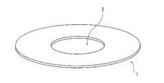
- FIG. 1 is a view showing the external shape of the magnetic disk substrate of the present embodiment.
- a magnetic disk substrate 1 (hereinafter simply referred to as a substrate 1) in the present embodiment is a disk-like thin plate substrate in which an inner hole 2 is formed.
- the substrate 1 can be suitably applied to, for example, a substrate for a magnetic disk having a nominal diameter of 2.5 inches or 3.5 inches.
- the outer diameter (diameter) of the disk shape is preferably 90 mm or more.
- the nominal value of the disc-shaped outer diameter can be 95 mm or 97 mm.
- the upper limit of the outer diameter (diameter) of the disk shape is, for example, 100 mm. Since the width of a general 3.5-inch HDD (size that can be mounted in a 3.5-inch bay of a general PC case) is 101.6 mm, if it exceeds 100 mm, there is a risk that the wall thickness may not be sufficient. The vibration of the magnetic disk generated by the external impact different from the flutter vibration becomes larger as the outer diameter of the substrate 1 becomes larger, and the damping becomes difficult.
- the magnetic disk substrate of the present embodiment is particularly preferable for a magnetic disk substrate having a nominal size of 3.5 inches or more.
- FIG. 2 is a view for explaining an example of an end portion of the substrate 1 and a film.
- the substrate 1 has a substrate body 3 and a film 4.
- Substrate body 3 is arranged between a pair of main surfaces 3a, a side wall surface 3b arranged along a direction orthogonal to the pair of main surfaces 3a, and a pair of main surfaces 3a and 3b. And a pair of beveled surfaces 3c.
- the side wall surface 3 b and the chamfered surface 3 c are formed at the end on the outer peripheral side and the end on the inner peripheral side of the substrate 1.
- the glass composition of the substrate main body 3 for example, by mol%, a SiO 2, 55 ⁇ 78%, the Li 2 O, 0.1 ⁇ 1% , the Na 2 O, 2 10% to 25% in total including MgO, CaO, SrO and BaO, and the molar ratio of CaO content to the total content of MgO, CaO, SrO and BaO (CaO / (MgO + CaO + SrO + BaO)) is 0 .20 or less.
- This glass is called glass 1.
- the glass of the substrate main body 3 for example, by mol%, a SiO 2 45 ⁇ 68%, the Al 2 O 3 5 ⁇ 20% , the total content of SiO 2 and Al 2 O 3 (SiO 2 + Al 2 O 3 ) 60-80%, B 2 O 3 0-5%, MgO 3-28%, CaO 0-18%, and total content of BaO and SrO (BaO + SrO) 0-2% 12-30% of the total content of alkaline earth metal oxides (MgO + CaO + SrO + BaO), 3.5-15% of the total content of alkali metal oxides (Li 2 O + Na 2 O + K 2 O), Sn oxides and Ce It can also be an amorphous oxide glass containing at least one selected from the group consisting of oxides, and having a total content of Sn oxide and Ce oxide of 0.05 to 2.00%. This glass is called glass 2.
- a film 4 is provided on the entire surface of the substrate main body 3, that is, the main surface 3a, the side wall surface 3b, and the chamfered surface 3c.
- the film 4 enhances the anti-vibration characteristics of the substrate 1.
- the film 4 is a film of a material having a loss coefficient value of 0.01 or more.
- the membrane is composed of a metallic material.
- the metal material of the film 4 is a material having a higher loss coefficient than the material of the substrate body 3.
- the value of the loss factor is that at room temperature, eg 25 ° C.
- the loss factor refers to the value at room temperature.
- the loss coefficient of the film 4 is obtained by determining the resonance frequency and the half value width at the resonance frequency of the test sample by a vibration test using each of the substrate body 3 and the substrate 1 having the film 4 formed on the substrate body 3 as a test sample.
- a vibration test for example, "Free resonant type Young's modulus, rigidity and internal friction measuring device (JE series)" manufactured by Nippon Techno Plus Co., Ltd. can be used.
- the loss factor of the test sample is determined from the resonant frequency and half width of the test sample obtained in the vibration test.
- the resonant frequency and loss coefficient of the substrate 1, the resonant frequency of the substrate body 3, the ratio of the thickness of the substrate body 3 to the thickness of the film 4, the density of the material of the substrate body 3 and the density of the metal material of the film 4 can be calculated, for example, according to a known equation shown below.
- a Ni—P alloy containing Ni and P can be suitably used as a material having such characteristics (loss coefficient) of the film 4.
- P may be contained so as to be nonmagnetic.
- the content of P can be 5 to 15% by mass.
- a metal material of the film 4 an Mg alloy, an Al—Zn alloy, an Mg—Zr alloy or the like can be used as a metal material of the film 4.
- a film formation method for example, a sputtering method, an electroless plating method, an electrolytic plating method, or the like can be used. It may be appropriately selected from these.
- the thickness T of the substrate 1 including the substrate body 3 and the film 4 is 0.700 mm or less. Furthermore, the thickness D [mm] of the film 4 provided on the main surface 3a and the thickness T [mm] of the substrate 1 including the film 4 satisfy the following formula (1). The thickness of the film 4 does not change depending on the location of the main surface, and is preferably constant on the main surface. D 0.00 0.0082 / T-0.0015 (1)
- the film 4 is formed, the above-mentioned vibration can be attenuated early. Furthermore, it is preferable that the film 4 continuously cover the entire circumference of the metal main body 1 including the end face, because the degree of suppression of the above-mentioned vibration becomes particularly high. Further, in this case, it is more preferable that the film 4 be harder than the substrate body 3. More preferably, the thicknesses D1 and D2 of the films 4 formed on the main surfaces 3a on both sides of the substrate main body 3 are equal.
- the film 4 is formed on each of the main surfaces 3a on both sides, but the present embodiment also includes a configuration in which the film 4 is formed on only one of the main surfaces 3a.
- the thickness D of the film 4 is the thickness of the film 4 formed on one of the main surfaces 3a.
- a magnetic disk produced by forming a magnetic film on the substrate 1 is fixed to the spindle of the hard disk drive on the main surface in the vicinity of the inner hole 2 in the hard disk drive.
- the external impact is accompanied by those operations.
- Hard disk drive devices may receive. Such an impact generates a vibration in which the main surface 3a of the substrate 1 is displaced in the normal direction (the thickness direction of the substrate 1) of the main surface 3a. This displacement is largest at the outer peripheral end face of the main surface.
- FIG. 3 is a view showing an example of vibration in the normal direction of the main surface at the outer peripheral end of the substrate 1.
- Such vibrations occur whether the magnetic disk is rotating or stationary. For this reason, it is not preferable that this vibration continues for a long time and the magnetic disk formed from the substrate 1 contacts the ramp member in the hard disk drive to cause particles, scratches and dents on the surface of the magnetic disk.
- the lamp member may be scraped or the like due to this contact to generate a puddle.
- the stationary magnetic disk vibrates and contacts the ramp member, the same location of the magnetic disk contacts the ramp member many times, so particles, scratches and dents tend to occur in many cases. .
- the substrate 1 is the film 4 made of a metal material having a loss coefficient value of 0.01 or more
- the smaller the thickness T the larger the amplitude due to vibration and the more difficult it is to damp the amplitude.
- the value of the loss factor of the film 4 is preferably 0.02 or more.
- the upper limit of the loss factor value of the film 4 is not particularly limited, but a material having an excessively large loss factor value may be a soft material in which crystals in the metal material are easily broken. If the hardness of the film 4 is too low, the surface is easily damaged after forming the magnetic disk, which may cause a crash of the HDD. For this reason, it is preferable that it is 0.3 or less from the point which can use a practical metal material.
- the thickness D is less than 0.0082 / T-0.0015, the thickness D of the film 4 is not sufficiently thick with respect to the thickness T of the substrate body 3, so that the vibration in the substrate 1 is damped early. Besides being difficult, the membrane 4 can not reduce the initial amplitude of the oscillation of the main surface 3a.
- the thickness D is 0.0082 / T-0.0015 or more, the thickness of the film 4 covering the main surface 3a becomes sufficient, so that the vibration in the substrate 1 is damped at an early stage, and The amplitude can be kept small.
- the number of times the magnetic disk contacts the external member such as the ramp member due to the vibration of the magnetic disk can be effectively reduced even if the thickness of the substrate is reduced.
- the thickness D is preferably 0.0094 / T or more.
- the thickness D is preferably 0.0094 / T or more.
- the film thickness of the magnetic film or the like on any one surface is 0.1 ⁇ m or less in total, so in this specification, The impact on the vibration in question can be ignored. That is, the vibration characteristic is the same as that of the substrate 1 even after forming the magnetic disk.
- FIG. 4 is a view for explaining the range of the thickness T [mm] and the thickness D [mm] of the substrate 1 of the present embodiment.
- the range in the present embodiment is the upper region indicated by the arrow with respect to the solid curve in FIG.
- the lower the thickness T the thicker the lower limit of the thickness D.
- the film 4 can be provided only on the main surface 3a and not on the side wall surface 3b and the chamfered surface 3c, the above effect can be obtained, but the film 4 covers the entire surface of the substrate 1 as shown in FIG. It is preferable to be provided continuously, that is, continuously to the end face of the substrate main body 3, that is, the side wall surface 3b and the chamfered surface 3c, in addition to the main surface 3a.
- the vibration generated in the substrate 1 is vibration displaced in the normal direction of the main surface 3a, and the method of the main surface 3a in the end surface of the substrate main body 3 in conjunction with the displacement in the normal direction of the main surface 3a in this vibration. Displace in the linear direction.
- the film 4 By providing the film 4 not only on the main surface 3a but also on the end face of the substrate body 3, ie, the side wall surface 3b and the chamfered surface 3c, the amount of displacement in the normal direction of the main surface 3a, ie, the amplitude of vibration is It can be suppressed. It is presumed that the vibration suppression effect of the film 4 is enhanced by connecting the two main surfaces with the film 4.
- the thickness of film 4 on side wall surface 3b and chamfered surface 3c is preferably thicker than thicknesses D1 and D2 on each of main surface 3a.
- the vibration generated in the substrate 1 is vibration displaced in the normal direction of the main surface 3a, and the method of the main surface 3a in the end surface of the substrate main body 3 in conjunction with the displacement in the normal direction of the main surface 3a in this vibration. Displace in the linear direction. By suppressing such displacement, the amount of displacement in the normal direction of main surface 3a, that is, the amplitude of vibration can be suppressed. Therefore, in addition to main surface 3a, the end face of substrate main body 3, that is, the side It is preferable that the film 4 be formed also on the wall surface 3 b and the chamfered surface 3 c.
- the film thickness at the end face (side wall surface 3b and chamfered surface 3c) of the substrate main body 3 is 110% or more of the film thicknesses D1 and D2 (the film thickness of the thicker one when the film thicknesses D1 and D2 are different) on the main surface 3a.
- the membrane 4 is provided to Thereby, the amplitude of the vibration can be suppressed without affecting the thickness T of the substrate 1.
- substrate body 3 is 150% or less of film thickness D1, D2 in the main surface 3a.
- the mass produced at the end of the outer periphery of the substrate 1 causes the substrate 1 to rotate as a magnetic disk The force is increased, and this centrifugal force is not preferable because the flutter vibration is likely to be increased.
- the thickness of the substrate 1 is It may be 0.570 mm or less, further 0.52 mm or less, and 0.400 mm or less.
- the thickness of the substrate 1 can be, for example, 0.635 mm or less, 0.550 mm or less, 0.500 mm or less, and 0.381 mm or less.
- the lower limit of the thickness of the substrate 1 is preferably 0.2 mm or more from the viewpoint of mechanical durability. As the substrate 1 becomes thinner, the problem of particle generation and, in some cases, the generation of flaws and dents may increase in principle, but in the present embodiment, the effect of reducing particles, flaws and dents is remarkable. Become. Assuming that the thickness T of the substrate 1 is 0.640 mm or less, the height of a general 3.5 inch HDD is 26.1 mm (size that can be mounted in the 3.5 inch bay of a general PC case), The gap between the ramp members, which will be described later, is preferable because the number of mounted substrates can be increased from eight to nine in the thickness of the magnetic disk plus 0.4 mm.
- the height of the HDD is set to 26.1 mm or more, it is also possible to set the number of mounted sheets to 9 or more.
- the thickness of the substrate is set to 0.520 mm or less, it is more preferable because the number of mounted substrates can be 10 or more in the same size HDD as described above. Since these HDDs carry more substrates than in the past, contact between the disk and the ramp member or the adjacent disk is likely to increase when it receives an external impact, and the failure (particle, There is a problem that scratches, dents) are easily generated, but using the substrate of the present embodiment makes it possible to reduce the number of obstacles.
- the Vickers hardness Hv of the film 4 is preferably 100 [kgf / mm 2 ] or more.
- the Vickers hardness Hv By increasing the Vickers hardness Hv, defects such as scratches and dents are less likely to occur when in contact with a lamp member or the like in the hard disk drive.
- the Vickers hardness Hv is less than 100 [kgf / mm 2 ]
- a defect such as a scratch or a dent occurs when contacting with a lamp member or the like in the hard disk drive, and the failure of the hard disk drive tends to occur.
- the maximum height Rz (JIS B 0601: 2001) of the surface roughness of the outer peripheral end face forming the interface with the film 4 of the disk-shaped substrate body 3 is 0.5 ⁇ m or more. Is preferred.
- the roughness of the substrate body 3 at the interface with the film 4 is referred to as the surface roughness of the outer peripheral end face of the substrate body 3 forming the interface with the film 4.
- the film 4 is formed on the substrate main body 3 including the outer peripheral end face, a cross-sectional image of the outer peripheral end face of the substrate main body 3 can be obtained by the method described below, and the maximum height Rz can be obtained. .
- the outer peripheral end face of the substrate 1 provided with the film 4 is cut out in a plane perpendicular to the main surface through the center of the substrate 1 using the ion polishing method, and the cross section of the outer peripheral end face is exposed Make a sample.
- a scanning electron microscope (SEM) is used to obtain a cross-sectional image of the outer peripheral end face, for example, at a magnification of 5000 times.
- the unevenness curve of the surface of the substrate body 3 which forms the interface in contact with the film 4 of the substrate body 3 is acquired by performing, for example, a binarization process of a cross-sectional image or a visual trace process.
- An area of 20 ⁇ m in any place of is extracted to obtain the maximum height Rz.
- the presence of surface irregularities to a certain extent at the interface of the substrate body 3 in contact with the film 4 enhances the suppression of the vibration by the film 4.
- the suppression of the vibration is because the adhesion between the both is enhanced by penetrating into and recessed into each other at the interface between the substrate body 3 and the film 4, and the effect of suppressing the vibration by the film 4 affects the substrate body 3. It is guessed that.
- the film stress that causes film peeling is increased by thickening the film 4, but film peeling due to film stress can also be prevented by setting the maximum height Rz to 0.5 ⁇ m or more.
- the outer peripheral end face is smaller in area as compared with the main surface and has a complicated shape, and the thickness of the substrate 1 is 0.700 mm or less, which is thinner than the conventional one.
- the maximum height Rz of the surface roughness of the outer peripheral end face of the substrate main body 3 is more preferably 1.0 ⁇ m or more, and further preferably 1.5 ⁇ m or more, in order to increase the suppression of the above-mentioned vibration. preferable.
- the surface roughness of the film 4 after film formation (the surface roughness of the outer peripheral end face of the substrate 1) becomes large following the surface roughness of the substrate main body 3 and the main surface
- the surface roughness of the film 4 after film formation becomes large following the surface roughness of the substrate main body 3 and the main surface
- foreign substances are easily attached to the outer peripheral end face at the time of processing such as polishing, and also at the outer peripheral end face even in the magnetic disk after forming the magnetic film.
- the yield of The location of the outer peripheral end face where the maximum height Rz is 0.5 ⁇ m or more may be at least a part of the outer peripheral end face, but in order to enhance the suppression of the vibration and enhance the film peeling preventing effect, It is preferable that both the side wall surface 3b and the chamfered surface 3c be provided.
- the maximum height Rz on the main surface of the substrate body 3 is too large, a defect may be formed at the initial stage of formation of the film 4 and propagate to cause defects such as recesses and cracks on the surface of the film 4 There is.
- the maximum height Rz it is preferable to remove these defects because they cause corrosion and surface defects after polishing, but since the roots are deep and it is difficult to remove them, the influence remains even after the magnetic film is formed into a magnetic disk. . Therefore, it is preferable to set the maximum height Rz to, for example, 1 ⁇ m or less on the main surface of the substrate main body 3.
- the maximum height Rz of the surface roughness of the film 4 at the outer peripheral end surface of the substrate 1 is the surface roughness of the substrate main body 3 at the outer peripheral end surface (the interface in contact with the film 4) of the substrate main body 3
- it is smaller than the maximum height Rz of
- the maximum height Rz of the surface roughness of the film 4 at the outer peripheral end face of the substrate 1 is, for example, a plurality of points (for example, 3)
- the maximum height Rz of the portion 4) is determined, and the average value of the plurality of portions is set as the maximum height Rz of the surface roughness of the film 4.
- the movement (scanning) direction of the stylus is the thickness direction of the nonmagnetic substrate 1.
- the maximum height Rz of the surface roughness of the film 4 at the outer peripheral end face of the substrate 1 is excessively large, foreign matter adhesion to the substrate 1 or scratches due to gripping of the outer peripheral end face in the subsequent steps such as formation of a magnetic film.
- the above-mentioned maximum height Rz is preferably small because it tends to be a factor. Therefore, the maximum height Rz of the surface roughness of the film 4 at the outer peripheral end face of the substrate 1 is greater than the maximum height Rz of the surface roughness of the substrate main body 3 at the outer peripheral end face of the substrate main body 3 (the interface in contact with the film 4). It is preferable to make it smaller.
- the maximum height Rz is more preferably 1.0 ⁇ m or less, and still more preferably 0.5 ⁇ m or less.
- the location of the outer peripheral end face of the substrate 1 for limiting the maximum height Rz may be at least a part of the outer peripheral end face of the substrate 1, but in order to enhance the effect of suppressing the vibration and enhance the effect of preventing film peeling.
- it is a surface portion of the film 4 formed on the surface of the substrate 1 and on both the side wall surface 3b and the chamfered surface 3c.
- the surface roughness of the film 4 at the outer peripheral end face easily follows the surface roughness of the substrate main body 3 which is the base. Therefore, if the surface roughness of the substrate body 3 is too large, additional processing such as end face polishing may be required after the formation of the film 4.
- the substrate 1 has a disk shape with an outer diameter of 90 mm or more, and the thickness of the substrate 1 is 0.700 mm or less.
- the film 4 is provided so as to have a characteristic that the number of displacements by vibration becomes 0.2 mm or more four times or less. For example, the loss factor and the film thickness of the film 4 are set to realize the above characteristics.
- the number of times the displacement amount is 0.2 mm or more is 4 or less, because the number of repeated contacts at the same position with the external member is 2 or less. More preferably, the number of times the displacement amount is 0.2 mm or more is 2 times or less. When the number of times is 2 or less, it means that there is no contact on a surface of the substrate 1 a plurality of times. That is, in the magnetic disk, since there are no repeated collisions at the same position on the main surface, it is more preferable that the number of times the displacement amount is 0.2 mm or more is 2 or less.
- the characteristic of the substrate body 3 is that, when the above-described impact is applied to the substrate body 3, the number of times the displacement amount by the vibration in the thickness direction of the outer peripheral end of the substrate body is 0.2 mm or more is four times. It may be more than one.
- the film 4 in which the material and thickness of the film are adjusted, the number of times the displacement amount becomes 0.2 mm or more can be suppressed to 4 times or less.
- the substrate 1 has a disk shape with an outer diameter of 90 mm or more and a thickness of 0.700 mm or less, the displacement due to the vibration in the thickness direction of the outer peripheral end of the substrate 1 tends to increase.
- the substrate 1 is limited by the effect of the film 4 to 4 times or less the amount of displacement due to vibration is 0.2 mm or more.
- Such a substrate 1 is produced, for example, as follows.
- a glass substrate which is a material of a plate-like glass substrate for a magnetic disk having a pair of main surfaces is performed.
- rough grinding of this glass blank is performed.
- the glass blank is subjected to shape processing and end face polishing.
- the fine grinding using the fixed abrasive is performed on the glass substrate obtained from the glass blank.
- the first polishing, the chemical strengthening, and the second polishing are applied to the glass substrate. After this, film formation and film polishing are performed.
- the said process does not need to be always and these processes do not need to be performed suitably.
- the end face polishing, the fine grinding, the first polishing, the chemical strengthening, and the second polishing may not be performed.
- A Forming of Glass Blank
- a press forming method can be used.
- a circular glass blank can be obtained by the press molding method.
- it can manufacture using well-known manufacturing methods, such as the down draw method, the redraw method, and the fusion method.
- a disk-shaped glass substrate to be a base of a glass substrate for a magnetic disk can be obtained by appropriately performing shape processing on a plate-shaped glass blank made by these known manufacturing methods.
- (B) Rough grinding In rough grinding, the main surfaces on both sides of the glass blank are ground. For example, loose abrasive is used as the abrasive. In rough grinding, the glass blank is ground so as to approximate the target thickness dimension and the flatness of the main surface. In addition, rough grinding is performed according to the dimensional accuracy or surface roughness of the shape
- shape processing is performed.
- shape processing after forming a glass blank, a circular hole is formed using a known processing method to obtain a disk-shaped glass substrate having a circular hole. Thereafter, chamfering of the end face of the glass substrate is performed. Thereby, on the end face of the glass substrate, a chamfered surface 3c inclined with respect to the main surface 3a is formed between the side wall surface 3b orthogonal to the main surface and the side surface 3b and the main surfaces 3a on both sides. Be done.
- end face polishing of the glass substrate is performed.
- a polishing liquid containing loose abrasive is supplied between the polishing brush and the end face of the glass substrate (side wall surface 3b and the chamfered surface 3c) to move the polishing brush relative to the glass substrate.
- the end face polishing the inner peripheral side end face and the outer peripheral side end face of the glass substrate are to be polished, and the inner peripheral side end face and the outer peripheral side end face are in a mirror state. Note that the end face polishing may not be performed depending on circumstances.
- the main surface of the glass substrate is subjected to fine grinding.
- grinding is performed on the main surface 3a of the glass substrate using a double-side grinding device of a planetary gear mechanism.
- fixed abrasive is provided on a platen and is ground.
- grinding using loose abrasive can also be performed. Fine grinding may not be performed depending on circumstances.
- the first polishing is applied to the main surface 3a of the glass substrate.
- the first polishing uses a polishing pad attached to a surface plate using loose abrasive grains.
- the surface roughness of the main surface 3a for example, the arithmetic average roughness Ra can be reduced while preventing the shape of the end portion of the main surface 3a from being excessively depressed or protruded.
- the free abrasive used in the first polishing is not particularly limited, and, for example, cerium oxide abrasive or zirconia abrasive is used. The first polishing may not be performed depending on circumstances.
- the glass substrate can be chemically strengthened as appropriate.
- a chemical strengthening solution for example, a molten solution obtained by heating potassium nitrate, sodium nitrate or a mixture thereof can be used. Then, by immersing the glass substrate in the chemical strengthening solution, lithium ions and sodium ions in the glass composition on the surface layer of the glass substrate become sodium ions and potassium ions having relatively large ion radius in the chemical strengthening solution. By being replaced, a compressive stress layer is formed on the surface layer portion, and the glass substrate is strengthened.
- the timing of chemical strengthening can be determined as appropriate, but it is particularly preferable to perform polishing after chemical strengthening, since foreign substances adhering to the surface of the glass substrate can be removed by chemical strengthening as well as smoothing of the surface. . Also, chemical strengthening may not be necessary in some cases.
- the second polishing is applied to the chemically strengthened glass substrate.
- the second polishing aims at mirror polishing of the main surface 3a.
- polishing is performed using a polishing apparatus having the same configuration as the first polishing.
- the type and particle size of the loose abrasive are changed with respect to the first polishing, and mirror polishing is performed using a material having a soft resin polisher as a polishing pad.
- the roughness of the main surface 3a is preferably 0.2 nm or less as arithmetic mean roughness Ra (JIS B 0601 2001).
- the second polishing since the main surface 3a of the substrate after the second polishing does not become the outermost surface of the substrate 1 having the film 4, the second polishing may not be performed depending on circumstances.
- the film 4 is formed on the main surface 3a, the side wall surface 3b, and the chamfered surface 3c of the manufactured glass substrate.
- the film 4 is formed by electrolytic plating, electroless plating, sputtering or the like. Before the formation of the film 4, a pretreatment for improving the adhesion of the film 4 or the formation of an underlayer may be performed as necessary.
- the film 4 is formed on the main surface 3a, the side wall surface 3b, and the chamfered surface 3c, and can have the same film thickness on any of the surfaces.
- annealing (heat treatment) of the film 4 is performed as necessary.
- the film 4 is preferably nonmagnetic so as not to cause noise when it is finally made into a magnetic disk.
- film polishing After the formation of the film 4, the film 4 on the main surface 3 a of the substrate body 3 is polished to reduce the surface roughness of the film 4.
- Film polishing aims at mirror polishing. Also in film polishing, polishing can be performed using a polishing apparatus having the same configuration as the first polishing. In the film polishing, the type and particle size of the loose abrasive are changed with respect to the first polishing, and polishing is performed using a material having a soft resin polisher as a polishing pad. In film polishing, multiple polishing may be performed as needed. In this case, as the polishing in the later step, the particle size of the free spit particles is made finer to carry out precise polishing.
- the thickness of the film 4 on the side wall surface 3b and the chamfered surface 3c can be It can be thicker than the thickness of the film 4 on the surface 3a.
- the film 4 formed on the side wall surface 3b and the chamfered surface 3c has an effect of suppressing the amplitude of the vibration of the main surface 3a of the substrate 1 as described above, so the film 4 on the side wall surface 3b and the chamfered surface 3c is
- the thickness of the film 4 is preferably set to a thickness that can suppress the amplitude of vibration of the main surface 3a.
- the substrate body 3 is an Al alloy substrate
- the substrate body 3 is manufactured by the following method. First, the Al alloy substrate to be the substrate body 3 is machined into a required size and shape by cutting. Thereafter, in order to improve the shape accuracy and the flatness of the substrate body 3, pressure heating annealing is performed. Furthermore, the end faces (inner peripheral end face and outer peripheral end face) of the substrate body 3 are ground and polished. In grinding of the end face, a grinding tool is supplied from a nozzle while rotating the rotating tool having abrasive grains fixed to the end face of the substrate main body 3 cut and processed as in the case of the glass substrate to supply substrate grinding fluid. Grind the end face.
- the chamfered surface of the substrate body 3 is formed by grinding using a full-shaped grindstone in which the shape of the end portion of the rotary tool is formed in advance into a chamfered shape. Furthermore, in order to reduce the surface roughness of the end face, a polisher made of non-woven fabric is adhered to the surface of the rotary tool, and the end face of the substrate body 3 is polished while supplying a polishing liquid in which loose abrasives are dispersed.
- the main surface of the substrate body 3 is ground and processed using a double-side grinding apparatus, and further using a double-side polishing apparatus using a resin polisher made of foamed polyurethane and a polishing solution containing alumina abrasive grains or colloidal silica abrasive grains. Polish several times and wash last.
- the substrate body 3 may be subjected to zincate treatment as pretreatment for forming the film 4.
- an annealing process is appropriately performed to relieve the internal stress of the film 4.
- polishing of main surface 3a is further performed. The polishing may be performed multiple times as needed for the substrate. Thereafter, cleaning is performed to manufacture the magnetic disk substrate 1.
- the film 4 may use Mg alloy, Al-Zn alloy, Mg-Zr alloy or the like in addition to the Ni-P alloy described above.
- the metal material of the film 4 is a material having a high loss coefficient and a loss coefficient of 0.01 or more compared to the substrate main body 3 from the viewpoint of suppressing the vibration of the substrate 1 according to one embodiment.
- the loss factor of the metal material of the film 4 is preferably 0.02 or more, more preferably 0.03 or more.
- the loss coefficient of the substrate body 3 is preferably 0.002 or less, and more preferably 0.001 or less. The smaller the loss coefficient of the substrate body 3 is, the higher the effect of suppressing the vibration by the film 4 is. Therefore, the smaller the loss coefficient of the substrate body 3, the better.
- the amorphous aluminosilicate glass substrate used for magnetic disks is, for example, 0.001 or less. Further, in the case of an Al--Mg alloy substrate for a magnetic disk, it is, for example, 0.002 or less.
- the Vickers hardness Hv of the material of the film 4 is preferably 100 [kgf / mm 2 ] or more, but 200 [kgf / mm], since particles, scratches and dents are less likely to occur. 2 ] or more is more preferable, and 400 [kgf / mm 2 ] or more is even more preferable.
- Table 1 below shows the properties of the material of the substrate body 3 and the materials that can be suitably used as the film 4.
- the loss factor shown in Table 1 below is calculated using the above-described calculation method of the loss factor.
- the value of the loss factor is at room temperature.
- the Vickers hardness Hv is measured using a micro Vickers hardness tester under the conditions of an indenter load of 10 gf for the thin film 4 and an indenter load of 300 gf for the substrate 3.
- the loss factor of the aluminosilicate glass is obtained from several glasses including the compositions of the above-mentioned glasses 1 and 2.
- the value of the typical loss factor in the case of the glass 2 is 0.0006, and Vickers hardness is 741 [kgf / mm ⁇ 2 >].
- the composition of the Al-Mg alloy is, for example, in mass%, Mg: 3.5-5%, Si: 0-0.05%, Fe: 0-0.1%, Cu: 0-0.12%, Mn : 0 to 0.3%, Cr: 0 to 0.1%, Zn: 0 to 0.5%, Ti: 0 to 0.1%, balance is Al.
- the composition of the Mg alloy is, by mass%, Mg: 91.57%, Al: 7.6%, Zn: 0.7%, Mn: 0.13%.
- the composition of the Al—Zn alloy is, in mass%, Al: 60%, Zn: 40%.
- the composition of the Mg-Zr alloy is, by mass%, 99.4% Mg, 0.6% Zn.
- the composition of the Ni-P alloy is, in mass%, Ni: 90%, P: 10%.
- an aluminosilicate glass or an Al-Mg alloy is used as the material of the substrate body 3, and a Ni-P alloy, a Mg alloy, an Al-Zn alloy, and a Mg-Zr alloy are used as the material of the film 4. It is understood that use is preferable in terms of suppression of vibration.
- Ni-P alloy, Al-Zn alloy, and Mg-Zr alloy have Vickers hardness Hv of 100 [kgf / mm 2 ] or more and are high, and are more suitable as the material of the film 4. It becomes difficult to produce a dent.
- the Ni-P alloy has a particularly high Vickers hardness Hv and is more suitable as a material of the film 4.
- Example 1 Various substrates were manufactured to examine the effect of the magnetic disk substrate 1 (Examples 1 to 21).
- An aluminum alloy Al--Mg alloy
- Al--Mg alloy was used as the material of the substrate body of the magnetic disk substrate 1.
- the film 4 was formed so as to cover the entire surface of the substrate body 3 with a uniform film thickness by electroless plating of a Ni—P alloy (P: 10 mass%, balance Ni). Thereafter, the main surfaces on both sides were polished using a double-side polishing apparatus, and 10% of the thickness of the film 4 was removed by polishing on each main surface.
- the final thickness of the film 4 was the same on the main surfaces on both sides, and the thickness of each film 4 was 90% of the thickness of the film 4 at the end face.
- the thickness of the film 4 at the end face is about 111% of the thickness of the film 4 at the main surface.
- the value of the loss factor of the Ni-P alloy satisfies 0.01 or more.
- the size of the produced substrate 1 is 95 mm in outer diameter and 25 mm in inner diameter (round hole diameter), and a chamfered surface is formed at the connection portion with both main surfaces in each of the outer peripheral end surface and the inner peripheral end surface. With respect to the specifications of this chamfered surface, when T is 0.64 mm or more, the angle to the main surface is 45 °, the radial length is 150 ⁇ m, and the length in the thickness direction is 150 ⁇ m.
- the angle to the main surface is 45 °
- the length in the radial direction is 100 ⁇ m
- the length in the thickness direction is 100 ⁇ m.
- the roughness of the outer peripheral end face was adjusted so that the maximum height Rz was 0.1 ⁇ m for both the surface of the substrate body 3 and the surface of the substrate 1.
- the produced substrate 1 was attached to an evaluation apparatus equipped with a high speed camera.
- this evaluation apparatus it is possible to apply an external impact of an arbitrary size, and the movement (vibration) of the outer peripheral end of the substrate generated along with that can be photographed as a moving image. Then, by analyzing the moving image, it is possible to measure the displacement of the outer peripheral end in the normal direction of the main surface.
- a lamp for a lamp loading mechanism of a magnetic head is incorporated, and when each magnetic disk is mounted, a gap of 0.2 mm is formed from both main surfaces. That is, the gap between the ramps into which the magnetic disk enters is the thickness of the magnetic disk + 0.4 mm.
- this gap is designed to be constant even if the thickness of the substrate changes.
- this lamp is not provided in the evaluation device. Therefore, it is judged by the displacement amount of the substrate whether the actual HDD is in contact with the lamp by the displacement amount of the substrate due to vibration, and if the displacement amount is less than 0.2 mm, the contact with the lamp occurs It can be judged that The thickness of the magnetic film or the like formed in the media step can be substantially ignored because it is about 100 nm or less even on the surface of an arbitrary one, including the underlayer and the soft magnetic layer. In this evaluation, the substrate was not rotated, and was evaluated in a stationary state.
- an impact test is performed in which an impact of 120 [G] in 2 [msec] is applied in the normal direction of the main surface of the substrate 1, and vibration in the normal direction of the main surface of the outer peripheral edge is obtained. It was measured.
- the measurement result is represented as waveform data as shown in FIG. From this waveform data, count the number of times the amount of displacement in any direction normal to the center of the amount of displacement 0 at the outer peripheral edge of the substrate is 0.2 mm or more, and use the following evaluation criteria It evaluated based on. In the example shown in FIG. 3, the number of counts is four.
- Examples 1, 4, 7, 10, 13, 16, and 19 in Table 2 are comparative examples, and the other examples are examples.
- each of Examples 1 to 21 in Table 2 excluding Examples 1, 4, 7, 10, 13, 16, and 19 has D D 0.0082. /T-0.0015, and all evaluation results passed. Furthermore, the evaluation results of Examples 3, 6, 9, 12, 15, 18, 21 satisfying D 0.00 0.0094 / T were excellent.
- Example 2 In order to investigate the effect of the substrate 1 using the glass material as the substrate body 3, various substrates were produced (Examples 22 to 30).
- the glass 1 described above was used as a glass material.
- the film 4 is formed by electroless plating using a Ni—P alloy (P: 10% by mass, balance Ni) in the same manner as in Experimental Example 1, and thereafter, in the same manner as in Experimental Example 1.
- the main surfaces on both sides were polished using a double-sided polishing apparatus, and the thickness of the film 4 was adjusted on each of the main surfaces.
- the evaluation was also evaluated by the number of counts using the same evaluation method as in Experimental Example 1. The evaluation results are shown in Table 3 below.
- Examples 22 to 30 in Table 2 Examples 22, 25 and 28 are comparative examples, and Examples 23, 24, 26, 27, 29, and 30 are all examples.
- T of the substrate was 0.400 to 0.640 mm
- each example except for Examples 22, 25, and 28 had D 0.00 0.0082 / T ⁇ 0.0015, and all evaluation results passed.
- the evaluation results of Examples 24, 27 and 30 satisfying D ⁇ 0.0094 / T were excellent. From the above evaluation results, the effect of the substrate 1 is clear.
- Example 3 The substrate 1 in which the maximum height Rz of the surface roughness of the outer peripheral end face forming the interface with the film 4 of the substrate main body 3 was variously prepared was manufactured and subjected to the peeling test to examine the effect of the maximum height Rz (Example 31-39).
- the aluminum alloy (Al—Mg alloy) used in Experimental Example 1 was used as the substrate body 3.
- the film 4 was formed in the same manner as in Experimental Example 1 so as to cover the entire surface of the substrate body 3 with a uniform film thickness, using a Ni—P alloy (P: 10 mass%, balance Ni).
- the maximum height Rz of the outer peripheral end face of the substrate 1 was adjusted by changing the size of the abrasive grains contained in the general-purpose grindstone used for end face grinding and the size of the abrasive grains used for the subsequent end face grinding. If the surface roughness of the outer peripheral end face forming the interface with the film 4 of the substrate main body 3 is variously adjusted, the surface roughness of the film 4 at the outer peripheral end face on the substrate 1 also changes (for example, the substrate main body 3 and the film When the roughness of the interface with 4 is increased, the surface roughness of the film 4 on the surface side of the substrate 1 is also increased), and the maximum height Rz of the surface roughness of the film 4 at the outer peripheral end face on the substrate 1 is 0.5 ⁇ m It adjusted by performing end face grinding suitably so that it might become the following.
- the peeling test of the film 4 on the outer peripheral end face of the produced substrate 1 was performed.
- the substrate 1 in which the film 4 on the outer peripheral end face is easily peeled off is not preferable from the viewpoint of the long-term reliability of the HDD. That is, when the films 4 on the outer peripheral end face partially peel off, the effect of connecting and linking the films 4 on the main surfaces on both sides of the substrate 1 is reduced, and the vibration suppressing effect may be deteriorated.
- the surface roughness of the film 4 on the outer peripheral end face of Examples 6, 9 and 12 shown in Table 4 is 0.1 ⁇ m in maximum height Rz value. Of the maximum height Rz was 0.5 ⁇ m.
Landscapes
- Chemical & Material Sciences (AREA)
- Inorganic Chemistry (AREA)
- Engineering & Computer Science (AREA)
- Metallurgy (AREA)
- Ceramic Engineering (AREA)
- Magnetic Record Carriers (AREA)
- Manufacturing Of Magnetic Record Carriers (AREA)
Priority Applications (11)
| Application Number | Priority Date | Filing Date | Title |
|---|---|---|---|
| CN202110659616.XA CN113362863B (zh) | 2017-06-30 | 2018-07-02 | 磁盘用基板和磁盘 |
| PH1/2019/502156A PH12019502156B1 (en) | 2017-06-30 | 2018-07-02 | Substrate for magnetic disks, and magnetic disk |
| US16/499,210 US11152026B2 (en) | 2017-06-30 | 2018-07-02 | Substrate for magnetic disks, and magnetic disk |
| PH1/2021/552253A PH12021552253A1 (en) | 2017-06-30 | 2018-07-02 | Substrate for magnetic disk, and magnetic disk |
| MYPI2019005195A MY196313A (en) | 2017-06-30 | 2018-07-02 | Substrate For Magnetic Disks, and Magnetic Disk |
| CN201880018389.9A CN110431627B (zh) | 2017-06-30 | 2018-07-02 | 磁盘用基板和磁盘 |
| JP2018557056A JP6467118B1 (ja) | 2017-06-30 | 2018-07-02 | 磁気ディスク用基板及び磁気ディスク |
| SG11201908016WA SG11201908016WA (en) | 2017-06-30 | 2018-07-02 | Substrate for magnetic disks, and magnetic disk |
| US17/472,567 US11694718B2 (en) | 2017-06-30 | 2021-09-10 | Substrate for magnetic disk, magnetic disk, and hard disk drive apparatus |
| US18/321,166 US12190923B2 (en) | 2017-06-30 | 2023-05-22 | Substrate for magnetic disk, magnetic disk, and hard disk drive apparatus |
| US18/970,882 US20250095682A1 (en) | 2017-06-30 | 2024-12-05 | Substrate for magnetic disk, magnetic disk, and hard disk drive apparatus |
Applications Claiming Priority (2)
| Application Number | Priority Date | Filing Date | Title |
|---|---|---|---|
| JP2017129613 | 2017-06-30 | ||
| JP2017-129613 | 2017-06-30 |
Related Child Applications (2)
| Application Number | Title | Priority Date | Filing Date |
|---|---|---|---|
| US16/499,210 A-371-Of-International US11152026B2 (en) | 2017-06-30 | 2018-07-02 | Substrate for magnetic disks, and magnetic disk |
| US17/472,567 Continuation US11694718B2 (en) | 2017-06-30 | 2021-09-10 | Substrate for magnetic disk, magnetic disk, and hard disk drive apparatus |
Publications (1)
| Publication Number | Publication Date |
|---|---|
| WO2019004484A1 true WO2019004484A1 (ja) | 2019-01-03 |
Family
ID=64742939
Family Applications (1)
| Application Number | Title | Priority Date | Filing Date |
|---|---|---|---|
| PCT/JP2018/025104 Ceased WO2019004484A1 (ja) | 2017-06-30 | 2018-07-02 | 磁気ディスク用基板及び磁気ディスク |
Country Status (7)
| Country | Link |
|---|---|
| US (4) | US11152026B2 (https=) |
| JP (4) | JP6467118B1 (https=) |
| CN (2) | CN110431627B (https=) |
| MY (1) | MY196313A (https=) |
| PH (2) | PH12021552253A1 (https=) |
| SG (1) | SG11201908016WA (https=) |
| WO (1) | WO2019004484A1 (https=) |
Cited By (3)
| Publication number | Priority date | Publication date | Assignee | Title |
|---|---|---|---|---|
| CN111540386A (zh) * | 2019-02-07 | 2020-08-14 | 株式会社东芝 | 盘装置 |
| WO2024202050A1 (ja) * | 2023-03-31 | 2024-10-03 | Hoya株式会社 | 情報記録媒体用ディスク、ディスク中間体、及び情報記録媒体用基板 |
| US12548595B2 (en) | 2019-09-25 | 2026-02-10 | Western Digital Technologies, Inc. | Magnetic recording apparatus comprising disk with reduced thickness and reduced disk flatness |
Families Citing this family (7)
| Publication number | Priority date | Publication date | Assignee | Title |
|---|---|---|---|---|
| PH12021552252A1 (en) * | 2017-03-31 | 2022-05-02 | Hoya Corp | Non-magnetic substrate for magnetic disk, and magnetic disk |
| WO2019004484A1 (ja) * | 2017-06-30 | 2019-01-03 | Hoya株式会社 | 磁気ディスク用基板及び磁気ディスク |
| JP6895918B2 (ja) * | 2018-03-23 | 2021-06-30 | 古河電気工業株式会社 | 磁気ディスク用アルミニウム合金基板、ディスク駆動装置、及び磁気ディスク用アルミニウム合金基板の製造方法 |
| MY208527A (en) | 2018-08-07 | 2025-05-14 | Hoya Corp | Substrate for magnetic disk and magnetic disk |
| CN115176310A (zh) * | 2020-03-06 | 2022-10-11 | 豪雅株式会社 | 玻璃间隔件的制造方法、玻璃间隔件和硬盘驱动器装置 |
| JP7037600B2 (ja) * | 2020-07-03 | 2022-03-16 | 株式会社Uacj | 磁気ディスク用基板及び当該磁気ディスク用基板を用いた磁気ディスク |
| WO2025150557A1 (ja) * | 2024-01-11 | 2025-07-17 | 株式会社Uacj | 磁気ディスク用ディスクブランク及び磁気ディスク |
Citations (5)
| Publication number | Priority date | Publication date | Assignee | Title |
|---|---|---|---|---|
| JPH08212518A (ja) * | 1995-02-03 | 1996-08-20 | Hitachi Ltd | 磁気記憶装置及び多層磁性層磁気記録媒体 |
| JP2006302358A (ja) * | 2005-04-18 | 2006-11-02 | Kobe Steel Ltd | 磁気記録媒体用Al合金基板および磁気記録媒体 |
| JP2010218657A (ja) * | 2009-03-18 | 2010-09-30 | Toshiba Corp | 磁気記録媒体の製造方法 |
| JP2012126626A (ja) * | 2010-12-17 | 2012-07-05 | Konica Minolta Advanced Layers Inc | 記録媒体用ガラス基板 |
| JP5939350B1 (ja) * | 2015-12-28 | 2016-06-22 | 旭硝子株式会社 | 磁気記録媒体用ガラス基板、磁気記録媒体 |
Family Cites Families (32)
| Publication number | Priority date | Publication date | Assignee | Title |
|---|---|---|---|---|
| JPS5939350B2 (ja) | 1978-09-26 | 1984-09-22 | 株式会社ダイフク | 搬送台車駆動装置 |
| US4882236A (en) * | 1988-02-10 | 1989-11-21 | Olin Corporation | Rigid magnetic recording disks and method of producing same |
| JPH0757233A (ja) * | 1993-08-19 | 1995-03-03 | Hitachi Ltd | 磁気記録媒体 |
| US5626943A (en) * | 1994-06-02 | 1997-05-06 | The Carborundum Company | Ultra-smooth ceramic substrates and magnetic data storage media prepared therefrom |
| US5759681A (en) | 1995-02-03 | 1998-06-02 | Hitachi, Ltd. | Magnetic recording medium and magnetic recording system using the same |
| US5747135A (en) * | 1995-12-08 | 1998-05-05 | Aluminum Company Of America | Thin film pretreatment for memory disks and associated methods |
| JPH09198640A (ja) * | 1996-01-16 | 1997-07-31 | Kobe Steel Ltd | 磁気ディスク |
| JPH10334445A (ja) * | 1997-06-02 | 1998-12-18 | Kobe Steel Ltd | 磁気ディスク用基板 |
| SG84541A1 (en) * | 1998-08-19 | 2001-11-20 | Hoya Corp | Glass substrate for magnetic recording medium, magnetic recording medium, and method of manufacturing the same |
| US6316097B1 (en) * | 1998-09-28 | 2001-11-13 | Seagate Technology Llc | Electroless plating process for alternative memory disk substrates |
| JP2003016633A (ja) | 2001-06-28 | 2003-01-17 | Asahi Glass Co Ltd | 磁気ディスク用ガラス基板及びその製造方法 |
| JP2003263713A (ja) * | 2002-03-08 | 2003-09-19 | Canon Inc | 円筒状磁気記録媒体およびその作製方法 |
| JP2005322364A (ja) * | 2004-05-11 | 2005-11-17 | Fuji Electric Device Technology Co Ltd | 垂直磁気記録媒体用ディスク基板、該基板を用いた垂直磁気記録媒体、および、それらの製造方法 |
| US7573674B1 (en) * | 2004-12-23 | 2009-08-11 | Maxtor Corporation | Storage disk having increased damping characteristics in a disk drive |
| US7564181B2 (en) * | 2005-04-08 | 2009-07-21 | Eastman Kodak Company | Performance enhancement layer for OLED devices |
| JP2007066390A (ja) * | 2005-08-30 | 2007-03-15 | Konica Minolta Opto Inc | 磁気記録媒体用基板、及び磁気記録媒体用基板の製造方法 |
| US20090117411A1 (en) * | 2005-12-19 | 2009-05-07 | Showa Denko K.K. | Magnetic disk substrate and magnetic disk thereof |
| JP4665886B2 (ja) * | 2006-10-27 | 2011-04-06 | 富士電機デバイステクノロジー株式会社 | 垂直磁気記録媒体、垂直磁気記録媒体用基板、および、それらの製造方法 |
| JP5029952B2 (ja) | 2007-09-06 | 2012-09-19 | 富士電機株式会社 | ガラス基板およびその製造方法、ならびに当該ガラス基板を用いた磁気ディスク |
| WO2009096217A1 (ja) * | 2008-01-29 | 2009-08-06 | Konica Minolta Opto, Inc. | 磁気記録媒体用基板の製造方法、及び磁気記録媒体 |
| JP2009230811A (ja) * | 2008-03-24 | 2009-10-08 | Konica Minolta Opto Inc | 金型部材 |
| AU2010357211B2 (en) * | 2010-07-09 | 2013-09-19 | Micro Motion, Inc. | A vibrating meter including an improved meter case |
| JP5029777B1 (ja) * | 2011-11-22 | 2012-09-19 | 旭硝子株式会社 | 磁気記録媒体用ガラス基板、および該磁気記録媒体用ガラス基板を用いた磁気記録媒体 |
| WO2013146089A1 (ja) | 2012-03-30 | 2013-10-03 | Hoya株式会社 | 磁気ディスク用ガラス基板、磁気ディスク、磁気ディスクドライブ装置 |
| JP6014385B2 (ja) * | 2012-05-14 | 2016-10-25 | 昭和電工株式会社 | 磁気記録媒体及び磁気記録再生装置 |
| SG10201701244VA (en) * | 2013-06-27 | 2017-04-27 | Hoya Corp | Disk-shaped glass substrate, magnetic-disk glass substrate, method for manufacturing magnetic-disk glass substrate, and magnetic disk |
| WO2015152316A1 (ja) * | 2014-03-31 | 2015-10-08 | Hoya株式会社 | 磁気ディスク用ガラス基板 |
| JP5915718B1 (ja) * | 2014-11-07 | 2016-05-11 | 旭硝子株式会社 | 磁気ディスク用ガラス基板及び磁気ディスク |
| TWI755466B (zh) | 2016-12-28 | 2022-02-21 | 日商東洋鋼鈑股份有限公司 | 硬碟用基板及使用其之硬碟裝置 |
| JP6832179B2 (ja) | 2017-02-03 | 2021-02-24 | 昭和電工株式会社 | 磁気記録媒体用基板およびハードディスクドライブ |
| PH12021552252A1 (en) * | 2017-03-31 | 2022-05-02 | Hoya Corp | Non-magnetic substrate for magnetic disk, and magnetic disk |
| WO2019004484A1 (ja) * | 2017-06-30 | 2019-01-03 | Hoya株式会社 | 磁気ディスク用基板及び磁気ディスク |
-
2018
- 2018-07-02 WO PCT/JP2018/025104 patent/WO2019004484A1/ja not_active Ceased
- 2018-07-02 SG SG11201908016WA patent/SG11201908016WA/en unknown
- 2018-07-02 MY MYPI2019005195A patent/MY196313A/en unknown
- 2018-07-02 CN CN201880018389.9A patent/CN110431627B/zh active Active
- 2018-07-02 JP JP2018557056A patent/JP6467118B1/ja active Active
- 2018-07-02 CN CN202110659616.XA patent/CN113362863B/zh active Active
- 2018-07-02 PH PH1/2021/552253A patent/PH12021552253A1/en unknown
- 2018-07-02 PH PH1/2019/502156A patent/PH12019502156B1/en unknown
- 2018-07-02 US US16/499,210 patent/US11152026B2/en active Active
-
2019
- 2019-01-10 JP JP2019002969A patent/JP7092689B2/ja active Active
-
2021
- 2021-09-10 US US17/472,567 patent/US11694718B2/en active Active
-
2022
- 2022-06-16 JP JP2022096972A patent/JP7326542B2/ja active Active
-
2023
- 2023-05-22 US US18/321,166 patent/US12190923B2/en active Active
- 2023-08-02 JP JP2023126136A patent/JP7595713B2/ja active Active
-
2024
- 2024-12-05 US US18/970,882 patent/US20250095682A1/en active Pending
Patent Citations (5)
| Publication number | Priority date | Publication date | Assignee | Title |
|---|---|---|---|---|
| JPH08212518A (ja) * | 1995-02-03 | 1996-08-20 | Hitachi Ltd | 磁気記憶装置及び多層磁性層磁気記録媒体 |
| JP2006302358A (ja) * | 2005-04-18 | 2006-11-02 | Kobe Steel Ltd | 磁気記録媒体用Al合金基板および磁気記録媒体 |
| JP2010218657A (ja) * | 2009-03-18 | 2010-09-30 | Toshiba Corp | 磁気記録媒体の製造方法 |
| JP2012126626A (ja) * | 2010-12-17 | 2012-07-05 | Konica Minolta Advanced Layers Inc | 記録媒体用ガラス基板 |
| JP5939350B1 (ja) * | 2015-12-28 | 2016-06-22 | 旭硝子株式会社 | 磁気記録媒体用ガラス基板、磁気記録媒体 |
Cited By (10)
| Publication number | Priority date | Publication date | Assignee | Title |
|---|---|---|---|---|
| CN111540386A (zh) * | 2019-02-07 | 2020-08-14 | 株式会社东芝 | 盘装置 |
| JP2020129423A (ja) * | 2019-02-07 | 2020-08-27 | 株式会社東芝 | ディスク装置 |
| CN111540386B (zh) * | 2019-02-07 | 2021-09-28 | 株式会社东芝 | 盘装置 |
| JP7077248B2 (ja) | 2019-02-07 | 2022-05-30 | 株式会社東芝 | ディスク装置 |
| US11386923B2 (en) | 2019-02-07 | 2022-07-12 | Kabushiki Kaisha Toshiba | Disk device |
| US11830529B2 (en) | 2019-02-07 | 2023-11-28 | Kabushiki Kaisha Toshiba | Disk device |
| US12205621B2 (en) | 2019-02-07 | 2025-01-21 | Kabushiki Kaisha Toshiba | Disk device |
| US12603106B2 (en) | 2019-02-07 | 2026-04-14 | Kabushiki Kaisha Toshiba | Disk device |
| US12548595B2 (en) | 2019-09-25 | 2026-02-10 | Western Digital Technologies, Inc. | Magnetic recording apparatus comprising disk with reduced thickness and reduced disk flatness |
| WO2024202050A1 (ja) * | 2023-03-31 | 2024-10-03 | Hoya株式会社 | 情報記録媒体用ディスク、ディスク中間体、及び情報記録媒体用基板 |
Also Published As
| Publication number | Publication date |
|---|---|
| PH12019502156A1 (en) | 2020-07-06 |
| US20210407544A1 (en) | 2021-12-30 |
| CN113362863A (zh) | 2021-09-07 |
| SG11201908016WA (en) | 2019-09-27 |
| US20230298623A1 (en) | 2023-09-21 |
| JP7326542B2 (ja) | 2023-08-15 |
| JP7595713B2 (ja) | 2024-12-06 |
| PH12021552253A1 (en) | 2023-10-23 |
| CN110431627B (zh) | 2021-07-02 |
| JP6467118B1 (ja) | 2019-02-06 |
| CN110431627A (zh) | 2019-11-08 |
| US20250095682A1 (en) | 2025-03-20 |
| MY196313A (en) | 2023-03-24 |
| JP7092689B2 (ja) | 2022-06-28 |
| US11694718B2 (en) | 2023-07-04 |
| CN113362863B (zh) | 2022-09-30 |
| JPWO2019004484A1 (ja) | 2019-06-27 |
| US12190923B2 (en) | 2025-01-07 |
| PH12019502156B1 (en) | 2024-06-14 |
| JP2019053813A (ja) | 2019-04-04 |
| JP2023133503A (ja) | 2023-09-22 |
| US20200027481A1 (en) | 2020-01-23 |
| JP2022120158A (ja) | 2022-08-17 |
| US11152026B2 (en) | 2021-10-19 |
Similar Documents
| Publication | Publication Date | Title |
|---|---|---|
| JP7326542B2 (ja) | 磁気ディスク用基板及び磁気ディスク | |
| JP7646914B2 (ja) | 磁気ディスク用非磁性基板及び磁気ディスク | |
| JP7733785B2 (ja) | 磁気ディスク用基板、磁気ディスク及びハードディスクドライブ |
Legal Events
| Date | Code | Title | Description |
|---|---|---|---|
| ENP | Entry into the national phase |
Ref document number: 2018557056 Country of ref document: JP Kind code of ref document: A |
|
| 121 | Ep: the epo has been informed by wipo that ep was designated in this application |
Ref document number: 18823309 Country of ref document: EP Kind code of ref document: A1 |
|
| NENP | Non-entry into the national phase |
Ref country code: DE |
|
| 122 | Ep: pct application non-entry in european phase |
Ref document number: 18823309 Country of ref document: EP Kind code of ref document: A1 |