WO2019003708A1 - レンズおよびレンズの製造方法 - Google Patents
レンズおよびレンズの製造方法 Download PDFInfo
- Publication number
- WO2019003708A1 WO2019003708A1 PCT/JP2018/019301 JP2018019301W WO2019003708A1 WO 2019003708 A1 WO2019003708 A1 WO 2019003708A1 JP 2018019301 W JP2018019301 W JP 2018019301W WO 2019003708 A1 WO2019003708 A1 WO 2019003708A1
- Authority
- WO
- WIPO (PCT)
- Prior art keywords
- film
- lens
- lens body
- flat surface
- inorganic
- Prior art date
- Legal status (The legal status is an assumption and is not a legal conclusion. Google has not performed a legal analysis and makes no representation as to the accuracy of the status listed.)
- Ceased
Links
Images




Classifications
-
- G—PHYSICS
- G02—OPTICS
- G02B—OPTICAL ELEMENTS, SYSTEMS OR APPARATUS
- G02B3/00—Simple or compound lenses
-
- G—PHYSICS
- G02—OPTICS
- G02B—OPTICAL ELEMENTS, SYSTEMS OR APPARATUS
- G02B5/00—Optical elements other than lenses
Definitions
- the present invention relates to a lens and a method of manufacturing the lens.
- the surface of the lens is subjected to various processes to improve the lens function.
- problems such as ghosting or flare may occur. It is known that these problems are caused by stray light caused by internal reflection of the lens unit.
- a configuration in which an anti-reflection film is formed on a light transmission surface of a lens is known as a lens that constitutes the lens unit.
- a dielectric multilayer film in which a plurality of two types of inorganic dielectric layers having different refractive indexes are alternately stacked is known.
- Patent Document 1 There is also known a configuration in which a surface other than the light transmitting surface of the lens is painted or polished (for example, see Patent Document 1).
- a configuration in which a hard coat film (inorganic film) is formed on the light transmission surface of the lens.
- the polymeric material which has light transmittance is known as a material of a lens.
- the polymer material can be molded into a large amount of lenses by molding using a mold. Moreover, it is possible to perform surface processing which suppresses internal reflection by transferring the fine unevenness
- the coefficient of thermal expansion of the lens containing the polymer material and the inorganic film such as the above-mentioned dielectric multilayer film and hard coat film differ greatly. Therefore, even if an inorganic film is formed on the light transmission surface of a lens containing a polymer material, the inorganic film can not follow the expansion and contraction of the lens due to the difference in thermal expansion coefficient, and the inorganic film is easily damaged and peeled off.
- a buffer layer is formed on the light transmission surface of a lens containing a polymer material to buffer the difference in thermal expansion coefficient between the lens and the inorganic film.
- a buffer layer can be obtained, for example, by spin coating a liquid mixture (mixture) in which an inorganic material and a polymer material (binder) are mixed.
- the function of the buffer layer can suppress the peeling of the inorganic film.
- the buffer layer can be made not to inhibit the light transmittance of the entire lens.
- the mixture of the inorganic material and the polymer material is spread by spin coating, and the asperities are buffered. There is a risk of being buried in the layer. If the refractive index of the mixture is made similar to that of the lens so that the light transmission of the lens is not inhibited, light is transmitted on the surface of the concavities and convexities buried by the mixture, and the effect of suppressing stray light can not be obtained.
- the inventors of the present invention have made intensive studies on a configuration that can suppress damage to an inorganic film and further suppress stray light in a lens that includes a polymer material and in which an inorganic film is formed, and completed the invention.
- a lens body containing a first polymer material, and a first film disposed on the surface of the lens body and containing a mixture of a second polymer material and an inorganic material And a second film which is an inorganic film disposed on the surface of the first film, and the lens body has a concave surface provided on one surface viewed along the optical axis of the lens body A flat surface provided on the one surface and continuous with the concave surface, at least a portion of the concave surface is covered with the first film, and the flat surface is exposed from the first film; A lens having a polishing mark is provided.
- a concave surface provided on one surface of the lens body containing the first polymer material, viewed along the optical axis of the lens body, and the concave surface
- a method of manufacturing a lens comprising: forming a second film, and polishing and removing the first film overlapping the flat surface and the second film overlapping the flat surface.
- a concave surface provided on one surface of the lens body containing the first polymer material as viewed along the optical axis of the lens body, and the concave surface provided on the one surface
- a method of manufacturing a lens comprising the steps of: polishing and removing; and forming a second film, which is an inorganic film, on the surface of the first film.
- the present invention it is possible to provide a lens including a polymer material and having an inorganic film formed on the surface. Moreover, the manufacturing method of the lens in which the polymeric film was included and in which the inorganic film was formed in the surface can be provided.
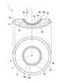
- FIG. 1 is a schematic view showing a lens of the embodiment.
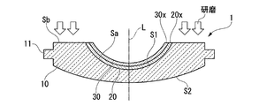
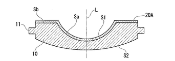
- FIG. 2A is a process chart showing a method of manufacturing a lens according to a second embodiment of the present invention.
- FIG. 2B is a process diagram showing a method of manufacturing a lens according to the second embodiment of the present invention.
- FIG. 2C is a process diagram showing a method of manufacturing a lens according to a second embodiment of the present invention.
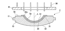
- FIG. 3 is an explanatory view of a lens 2 according to a third embodiment of the present invention.
- FIG. 4A is a process diagram showing a method of manufacturing a lens according to a fourth embodiment of the present invention.
- FIG. 4B is a process diagram showing a method of manufacturing a lens according to the fourth embodiment of the present invention.
- FIG. 4C is a process diagram showing a method of manufacturing a lens according to the fourth embodiment of the present invention.
- FIG. 1 is a schematic view showing a lens of the present embodiment.
- the lens 1 of the present embodiment includes a lens body 10, a first film 20, and a second film 30.
- the lens body 10 is a molded body containing a polymer material.
- the polymeric material which comprises the lens main body 10 is called "1st polymeric material.”
- thermoplastic resin any of a thermoplastic resin and a curable resin can be used.
- the curable resin may be thermosetting or photocurable.
- PMMA polymethyl methacrylate
- PC polycarbonate
- COP cyclic olefin polymer
- episulfide resin thiourethane resin
- thiourethane resin thiourethane resin
- an acrylic resin is preferable as the first polymer material because it is easy to process, has a high light transmittance, and is a material with little coloration.
- the lens body 10 using an acrylic resin as the first polymer material has high light transmittance and high quality.
- the first polymer material may be used in combination with various additives such as a stabilizer, an antioxidant, a filler, and a refractive index regulator as long as the light transmittance of the lens body 10 is not impaired.
- the lens body 10 has one surface S1 viewed along the optical axis L of the lens body 10, the other surface S2 opposite to the one surface S1, and one surface S1 extending in the circumferential direction of the lens body 10 And a circumferential surface S3 intersecting and intersecting with the other surface S2.
- One surface S1 includes a concave surface Sa which is visible along the optical axis L and overlaps the optical axis L, and a flat surface Sb which is disposed around the concave surface Sa and is continuous with the concave surface Sa. Looking at one surface S1 along the optical axis L of the lens body 10, the concave surface Sa is formed in a substantially circular shape centering on the position of the optical axis L.
- the other surface S2 is a convex surface.
- the concave surface Sa and the other surface S2 are light transmitting surfaces. That is, the lens body 10 is a so-called meniscus lens.
- the lens body 10 is a concave meniscus lens designed to have a curvature of the concave surface Sa larger than that of the other surface S2.
- the circumferential surface S3 may be a ground surface.
- the ridges 11 extending in the circumferential direction of the lens body 10 may be provided on the circumferential surface S3.
- the ridges 11 shown in FIG. 1 are configured in a closed ring shape.
- the first film 20 is a thin film containing a mixture of a polymer material and an inorganic material.
- membrane 20 is called "2nd polymeric material.”
- the second polymer material contained in the first film 20 is preferably a curable resin, more preferably a photocurable resin, and still more preferably an ultraviolet curable resin.
- fine particles of an inorganic oxide such as silica, zirconia, or titania can be used. These fine particles are dispersed in the second polymer material, for example, in the state of primary particles less than several tens of nm.
- Such an inorganic material is sufficiently small relative to the wavelength of light in the visible light range, and the light in the visible light range can be suitably transmitted as the entire first film 20.
- the first film 20 is disposed on the surface of the lens body 10. Specifically, the first film 20 covers the entire surface of the concave surface Sa of the lens body 10.
- the concave surface Sa is covered by the first film 20.
- the flat surface Sb is exposed from the first film 20.
- the first film 20 is not formed on the circumferential surface S3.
- the second film 30 is an inorganic film.
- the second film 30 is disposed on the surface of the first film 20.
- the second film 30 can adopt various configurations according to the function given to the lens 1.
- the second film 30 can be a dielectric multilayer film.
- the lens 1 can be provided with an antireflection function.
- a known configuration can be employed for the detailed configuration of the dielectric multilayer film.
- the second film 30 can also be a hard coat film for the purpose of preventing damage.
- the flat surface Sb, the end surface of the first film 20, and the end surface of the second film 30 are continuous surfaces. Looking at one surface S1 along the optical axis L of the lens body 10, the end face 20x of the first film 20 and the end face 30x of the second film 30 are concentrically exposed centering on the position of the optical axis L ing.
- the ends of the first film 20 and the second film 30 are not provided on the flat surface Sb, and the flat surface Sb, the end surface 20 x of the first film 20, and the end surface 30 x of the second film 30 And are continuous surfaces adjacent to each other.
- the lens 1 has a polishing mark on the flat surface Sb.
- the lens 1 configured as described above has the following function.
- the lens 1 has a first film 20 containing a second polymer material between the lens body 10 and the second film 30.
- the first film 20 buffers the difference in coefficient of thermal expansion between the lens body 10 containing the first polymer material and the second film 30 which is an inorganic film. Therefore, for example, when the lens 1 is used in a high temperature environment, it is possible to suppress the breakage (cracking, peeling) of the second film 30 caused by the difference in the thermal expansion coefficient between the lens body 10 and the second film 30. .
- the lens 1 has a polishing mark on the flat surface Sb.
- the flat surface Sb on which the polishing mark is formed functions as a light shielding surface that scatters light incident on the flat surface Sb and reduces the ratio of light passing through the flat surface Sb. Thereby, the light which injects into flat surface Sb becomes difficult to inject into the light transmissive surface (concave surface Sa, other surface S2) of the lens 1.
- the first film 20 is not formed on the circumferential surface S3 which is a ground surface, and the ground surface is maintained. Therefore, the circumferential surface S3 functions as a light shielding surface that scatters the light incident on the circumferential surface S3 and reduces the ratio of the light passing through the circumferential surface S3. Thereby, the light which injects into surrounding surface S3 becomes difficult to inject into the light transmissive surface (concave surface Sa, other surface S2) of the lens 1. As shown in FIG.
- the lens 1 having a polishing mark on the flat surface Sb is suppressed in stray light and has high quality.
- the lens 1 having the above-described configuration can suppress damage to the second film 30 which is an inorganic film, and can further suppress stray light.
- the first film 20 is described as covering the entire surface of the concave surface Sa.
- the first film 20 may be configured to cover at least a part of the concave surface Sa. Even when the portion covered by the first film 20 is at least a part of the concave surface Sa, the damage of the second film 30 can be suppressed by the lens 1 having the first film 20.
- FIG. 2A to FIG. 2C are process drawings showing a method of manufacturing a lens according to a second embodiment of the present invention.
- FIGS. 2A to 2C are described as manufacturing the lens 1 shown in FIG.
- the first film 20A is formed on one surface S1 (concave surface Sa and flat surface Sb).
- the first film 20A is formed by applying and forming a mixture of a precursor of the second polymer material which is a curable resin, an inorganic material, and, if necessary, a solvent (dispersion medium) as required. It is obtained by curing the first film 20A.
- solvent various solvents can be used as long as they can dissolve the precursor, and polar solvents can be suitably used.
- the solvent used for the above mixture include ketone solvents such as acetone, MEK (methyl ethyl ketone) and MIBK (methyl isobutyl ketone), and ether solvents such as diethyl ether, THF (tetrahydrofuran) and PGM (polypropylene glycol monomethyl ether).
- ester solvents such as methyl acetate and ethyl acetate. These solvents may be used alone or in combination of two or more.
- hydrocarbon solvents such as pentane and hexane
- aromatic solvents such as toluene and xylene may be further mixed with the above-mentioned solvent.
- the coating film of the mixture is formed by, for example, spin coating after dropping the above-mentioned mixture on the concave surface Sa.
- the first film 20A may be formed on the concave surface Sa by spin coating, and the first film 20A may not be formed on the flat surface Sb. In that case, it is necessary to strictly control the amount of the mixture dropped onto the concave surface Sa, the number of rotations at the time of spin coating, and the rotation time. Furthermore, in order to control the film thickness of the first film 20A formed on the concave surface Sa to a desired film thickness without forming the first film 20A on the flat surface Sb, more strict control is required.
- the first film 20A is positively formed on the flat surface Sb. Therefore, it is easy to form the first film 20A having a desired film thickness.
- a second film 30A is formed on the surface of the first film 20A.
- the second film 30A can be obtained, for example, by depositing the inorganic material IM using a known method such as vapor deposition or sputtering.
- the portion of the first film 20A overlapping with the flat surface Sb and the portion of the second film 30A overlapping with the flat surface Sb are polished away.
- the flat surface Sb is polished by pressing the flat surface Sb against a rotating polishing plate using a known polishing plate.
- a convex holder 11 is supported using a lens holder (not shown), and a force is applied to the convex rib 11 to press it against the polishing plate, thereby making the flat surface without touching the other surface S2 which is a light transmitting surface. Polishing of Sb is possible.
- the portion overlapping with the flat surface Sb is removed from the first film 20A, and the first film 20 shown in FIG. 1 is obtained.
- the portion overlapping the flat surface Sb is removed from the second film 30A, and the second film 30 shown in FIG. 1 is obtained.
- polishing marks are formed on the flat surface Sb. Polishing marks appear as a set of streaked marks (grooves) according to the movement of the rotating polishing plate.
- the depth of polishing marks or the density of grooves of polishing marks can be prepared by changing the conditions such as the type of polishing plate used for polishing, the stress pressing the lens against the polishing plate at the time of polishing, and the polishing time.
- the end portions of the first film 20 and the second film 30 are not provided on the flat surface Sb, and the flat surface Sb, the end surface 20 x of the first film 20, and the second
- the end face 30x of the film 30 is a continuous surface adjacent to each other.
- the lens manufacturing method of this embodiment is configured as described above.
- the lens manufacturing method as described above it is possible to easily manufacture the lens 1 provided with the second film 30 which is an inorganic film and further having the flat surface Sb which is a light shielding surface.
- FIG. 3 is an explanatory view of a lens 2 according to a third embodiment of the present invention.
- the same reference numerals as in the first embodiment denote the same constituent elements in the present embodiment, and a detailed description thereof will be omitted.
- the lens 2 of the present embodiment includes a lens body 10, a first film 20, and a second film 31.
- the first film 20 is provided between the lens body 10 and the second film 31.
- the second film 31 is an inorganic film similar to the second film 30 described above.
- the second film 31 covers the surface 20 y of the first film 20 and the end face 20 x of the first film 20, and covers a part of the flat surface Sb.
- the lens 2 has a polishing mark on the flat surface Sb.
- the lens 2 configured as described above has the following function.
- the first film 20 buffers the difference in coefficient of thermal expansion between the lens body 10 containing the first polymer material and the second film 31 which is an inorganic film. Therefore, for example, when the lens 2 is used in a high temperature environment, it is possible to suppress cracking and peeling of the second film 31.
- the flat surface Sb on which the polishing mark is formed in the lens 2 functions as a light shielding surface that scatters the light incident on the flat surface Sb and reduces the ratio of the light passing through the flat surface Sb.
- the lens 2 configured as described above can suppress damage to the second film 31 which is an inorganic film, and can further suppress stray light.
- FIG. 4A to FIG. 4C are process drawings showing a method of manufacturing a lens according to a fourth embodiment of the present invention. In FIGS. 4A to 4C, it will be described as manufacturing the lens 2 shown in FIG.
- the first film 20A is formed on the concave surface Sa of the lens body 10 and the flat surface Sb continuous with the concave surface Sa.
- polishing marks on the flat surface Sb can be prepared in the same manner as the lens manufacturing method of the second embodiment.
- a second film 31 is formed on the surface of the first film 20A.
- the second film 31 is obtained, for example, by depositing the inorganic material IM using a known method such as vapor deposition or sputtering via the mask M. As a result, a part of the flat surface Sb is exposed from the first film 20 and the second film 31.
- the lens manufacturing method of this embodiment is configured as described above.
- the lens manufacturing method as described above it is possible to easily manufacture the lens 2 which is provided with the second film 31 which is an inorganic film and further has a flat surface Sb which is a light shielding surface.
Landscapes
- Physics & Mathematics (AREA)
- General Physics & Mathematics (AREA)
- Optics & Photonics (AREA)
- Surface Treatment Of Optical Elements (AREA)
Abstract
本発明の一態様に係るレンズは、第1高分子材料を含むレンズ本体と、レンズ本体の表面上に配置され、第2高分子材料と無機材料との混合物を含む第1膜と、第1膜の表面上に配置された無機膜である第2膜と、を備える。レンズ本体は、レンズ本体の光軸に沿って視た一方の面に設けられた凹面と、一方の面に設けられ凹面と連続する平坦面と、を有する。凹面の少なくとも一部は、第1膜に覆われている。 平坦面は、第1膜から露出され、研磨痕を有する。
Description
本発明は、レンズおよびレンズの製造方法に関する。
通常、レンズの表面には、レンズ機能を向上させるために種々の加工が施されている。
例えば、複数のレンズを有するレンズユニットにおいては、ゴーストまたはフレアといった不具合を生じることがある。これらの不具合は、レンズユニットの内面反射に起因した迷光が原因であることが知られている。
このような迷光を抑制するため、レンズユニットを構成するレンズとして、レンズの光透過面に反射防止膜が形成された構成が知られている。反射防止膜としては、屈折率の異なる2種の無機誘電体層を交互に複数積層させた誘電体多層膜が知られている。
また、レンズの光透過面以外の面に、墨塗りを施したり、磨り加工したりする構成が知られている(例えば、特許文献1参照)。
その他、レンズ表面の傷つきを抑制するため、レンズの光透過面にハードコート膜(無機膜)を形成する構成が知られている。
ところで、レンズの材料として、光透過性を有する高分子材料が知られている。高分子材料は、金型を用いた成形加工により、大量にレンズを成形することが可能である。また、金型に予め形成した微細な凹凸をレンズに転写することで、内面反射を抑制する面加工を行うことが可能である。
しかし、高分子材料を含むレンズと、上述の誘電体多層膜、ハードコート膜などの無機膜とは、熱膨張率が大きく異なる。そのため、高分子材料を含むレンズの光透過面に無機膜を形成しても、熱膨張率の違いからレンズの膨張収縮に無機膜が追随できず、無機膜が破損、剥落しやすい。
本発明はこのような事情に鑑みてなされたものであって、高分子材料を含み、表面に無機膜が形成されたレンズを提供することを目的とする。また、高分子材料を含み、表面に無機膜が形成されたレンズの製造方法を提供することをあわせて目的とする。
上述の課題を解決する構成として、高分子材料を含むレンズの光透過面に、レンズと無機膜との熱膨張率差を緩衝する緩衝層を形成した構成が考えられる。このような緩衝層は、例えば、無機材料と高分子材料(バインダ)とを混合した液状混合物(混合物)をスピンコートすることにより得られる。
このような緩衝層を有するレンズでは、緩衝層の機能により、無機膜の剥落を抑制できると考えられる。また、緩衝層の屈折率をレンズに近似させ、光透過性を有する構成とすることにより、緩衝層がレンズ全体の光透過性を阻害しない構成とすることができる。
しかし、緩衝層を形成する面の周囲に、反射抑制のための微細な凹凸が形成されているレンズの場合、無機材料と高分子材料との混合物がスピンコートにより塗れ広がることで、凹凸が緩衝層に埋没してしまうおそれがある。混合物の屈折率をレンズに近似させることで、レンズの光透過性を阻害しない構成としていると、混合物により埋没した凹凸の表面では光を透過させてしまい、迷光を抑制する効果が得られない。
発明者らは、高分子材料を含み、無機膜が形成されたレンズにおいて、無機膜の損傷を抑制しさらに迷光を抑制可能な構成について鋭意検討を重ね、発明を完成させた。
すなわち、本発明の第1の態様によれば、第1高分子材料を含むレンズ本体と、前記レンズ本体の表面上に配置され、第2高分子材料と無機材料との混合物を含む第1膜と、前記第1膜の表面上に配置された無機膜である第2膜と、を備え、前記レンズ本体は、前記レンズ本体の光軸に沿って視た一方の面に設けられた凹面と、前記一方の面に設けられ前記凹面と連続する平坦面と、を有し、前記凹面の少なくとも一部は、前記第1膜に覆われ、前記平坦面は、前記第1膜から露出され、研磨痕を有するレンズが提供される。
本発明の第2の態様によれば、第1高分子材料を含むレンズ本体の、前記レンズ本体の光軸に沿って視た一方の面に設けられた凹面と、前記一方の面に設けられ前記凹面と連続する平坦面とに、第2高分子材料の前駆体と無機材料との混合物を塗布して成膜し、第1膜を形成する工程と、前記第1膜の表面に無機膜である第2膜を形成する工程と、前記平坦面と重なる前記第1膜および前記平坦面と重なる前記第2膜とを研磨して除去する工程と、を有するレンズの製造方法が提供される。
本発明の第3の態様によれば、第1高分子材料を含むレンズ本体の、前記レンズ本体の光軸に沿って視た一方の面に設けられた凹面と、前記一方の面に設けられ前記凹面と連続する平坦面とに、第2高分子材料の前駆体と無機材料との混合物を塗布して成膜し、第1膜を形成する工程と、前記平坦面と重なる前記第1膜を研磨して除去する工程と、前記第1膜の表面に無機膜である第2膜を形成する工程と、を有するレンズの製造方法が提供される。
本発明によれば、高分子材料を含み、表面に無機膜が形成されたレンズを提供することができる。また、高分子材料を含み、表面に無機膜が形成されたレンズの製造方法を提供することができる。
[第1実施形態][レンズ] 以下、図1を参照しながら、本発明の第1実施形態に係るレンズについて説明する。なお、以下の全ての図面においては、図面を見やすくするため、各構成要素の寸法、比率などは適宜異ならせてある。
図1は、本実施形態のレンズを示す模式図である。図に示すように、本実施形態のレンズ1は、レンズ本体10と、第1膜20と、第2膜30と、を備えている。
(レンズ本体) レンズ本体10は、高分子材料を含む成形体である。以下、レンズ本体10を構成する高分子材料を「第1高分子材料」と称する。
第1高分子材料は、熱可塑性樹脂および硬化性樹脂のいずれも用いることができる。硬化性樹脂は、熱硬化性であってもよく光硬化性であってもよい。
第1高分子材料としては、例えば、ポリメチルメタクリレート(PMMA)に代表されるアクリル系樹脂、ポリカーボネート(PC)、環状オレフィンポリマー(COP)等の熱可塑性樹脂、エピスルフィド系樹脂、チオウレタン系樹脂等の硬化性樹脂を用いることができる。
なかでも、加工が容易であること、高い光透過率を備えていること、着色が少ない材料であることから、第1高分子材料としてはアクリル系樹脂が好ましい。アクリル系樹脂を第1高分子材料として用いたレンズ本体10は、光透過率が高く高品質なものとなる。
また、レンズ本体10の光透過性を損なわない範囲において、第1高分子材料は、安定剤、酸化防止剤、フィラー、屈折率調整剤等の各種の添加剤と併用されることとしてもよい。
レンズ本体10は、レンズ本体10の光軸Lに沿って視た一方の面S1と、一方の面S1に対向する他方の面S2と、レンズ本体10の周方向に延在し一方の面S1および他方の面S2と交差して交わる周面S3とを有する。
一方の面S1は、光軸Lに沿って視て光軸Lと重なる凹面Saと、凹面Saの周囲に配置され凹面Saと連続する平坦面Sbと、を含む。レンズ本体10の光軸Lに沿って一方の面S1を視て、凹面Saは光軸Lの位置を中心とする略円形に形成されている。
また、レンズ本体10においては、他方の面S2は、凸面となっている。
レンズ本体10において、凹面Saおよび他方の面S2は、光透過面である。すなわち、レンズ本体10は、いわゆるメニスカスレンズである。また、レンズ本体10は、他方の面S2の曲率よりも凹面Saの曲率の方が大きく設計された凹メニスカスレンズである。
周面S3は、磨り面となっているとよい。磨り面である周面S3は、周面S3に入射する光を散乱させ、周面S3を透過する光の割合を低下させる遮光面として機能する。また、周面S3には、レンズ本体10の周方向に延在する凸条部11が設けられていてもよい。図1に示す凸条部11は、閉環状に構成されている。
(第1膜) 第1膜20は、高分子材料と無機材料との混合物を含む薄膜である。以下、第1膜20を構成する高分子材料を「第2高分子材料」と称する。
第1膜20に含まれる第2高分子材料は、硬化性樹脂であることが好ましく、光硬化性樹脂であることがより好ましく、紫外線硬化性樹脂であることがさらに好ましい。
第1膜20に含まれる無機材料としては、シリカ、ジルコニア、チタニア等の無機酸化物の微粒子を用いることができる。これらの微粒子は、例えば数十nm未満の一次粒子の状態で第2高分子材料に分散している。このような無機材料は、可視光領域の光の波長に対して充分に小さく、第1膜20全体として可視光領域の光を好適に透過させることができる。
第1膜20は、レンズ本体10の表面上に配置されている。詳しくは、第1膜20は、レンズ本体10の凹面Saの全面を覆っている。
本実施形態のレンズ1では、凹面Saは第1膜20に覆われている。また、レンズ1では、平坦面Sbは第1膜20から露出している。さらに、周面S3は、第1膜20が形成されていない。
(第2膜) 第2膜30は、無機膜である。第2膜30は、第1膜20の表面上に配置されている。
第2膜30は、レンズ1に付与する機能に応じて、種々の構成を採用することができる。例えば、第2膜30は、誘電体多層膜とすることができる。第2膜30が誘電体多層膜である場合、レンズ1に反射防止機能を付与することができる。誘電体多層膜の詳細な構成については、公知の構成を採用することができる。 その他、第2膜30は、傷付き防止を目的としたハードコート膜とすることもできる。
(レンズ) レンズ1において、平坦面Sb、第1膜20の端面、第2膜30の端面は、連続面となっている。レンズ本体10の光軸Lに沿って一方の面S1を視て、第1膜20の端面20x、および第2膜30の端面30xは、光軸Lの位置を中心とする同心状に露出している。
さらに、レンズ1では、平坦面Sbの上に第1膜20および第2膜30の端部が設けられず、平坦面Sbと、第1膜20の端面20xと、第2膜30の端面30xとは、互いに隣り合った連続面となっている。
また、レンズ1は、平坦面Sbに研磨痕を有する。
以上のような構成のレンズ1は、次のような機能を有する。
まず、レンズ1は、レンズ本体10と第2膜30との間に、第2高分子材料を含む第1膜20を有している。第1膜20は、第1高分子材料を含むレンズ本体10と、無機膜である第2膜30との熱膨張率の違いを緩衝する。そのため、例えばレンズ1を高温環境下で用いた場合に、レンズ本体10と第2膜30との熱膨張率の差に起因した第2膜30の破損(割れ、剥落)を抑制することができる。
また、レンズ1は、平坦面Sbに研磨痕を有する。研磨痕が形成された平坦面Sbは、平坦面Sbに入射する光を散乱させ、平坦面Sbを透過する光の割合を低下させる遮光面として機能する。これにより、平坦面Sbに入射する光は、レンズ1の光透過面(凹面Sa、他方の面S2)に入射しにくくなる。
また、レンズ1は、磨り面である周面S3に第1膜20が形成されておらず、磨り面が維持されている。そのため、周面S3は、周面S3に入射する光を散乱させ、周面S3を透過する光の割合を低下させる遮光面として機能する。これにより、周面S3に入射する光は、レンズ1の光透過面(凹面Sa、他方の面S2)に入射しにくくなる。
これらの構成により、平坦面Sbに研磨痕を有するレンズ1は、迷光が抑制され、高品質なものとなる。
さらに、第2膜30の端部が平坦面Sbの上に位置しないことで、平坦面Sbに第2膜30の膜厚に起因したニュートンリングが形成されず、高品位なレンズとなる。
したがって、以上のような構成のレンズ1は、無機膜である第2膜30の損傷を抑制し、さらに迷光を抑制可能となる。
なお、本実施形態においては、第1膜20は凹面Saの全面を覆うこととして説明したが、第1膜20は、凹面Saの少なくとも一部を覆っている構成であってもよい。第1膜20が覆う部分が凹面Saの少なくとも一部であっても、レンズ1が第1膜20を有することにより、第2膜30の損傷を抑制することが可能である。
[第2実施形態][レンズの製造方法] 図2A~図2Cは、本発明の第2実施形態に係るレンズの製造方法を示す工程図である。図2A~図2Cにおいては、図1に示すレンズ1を製造することとして説明する。
まず、図2Aに示すように、一方の面S1(凹面Saおよび平坦面Sb)に、第1膜20Aを形成する。
第1膜20Aは、硬化性樹脂である第2高分子材料の前駆体、無機材料、必要に応じてさらに溶媒(分散媒)を混合した混合物を塗布して成膜し、得られた塗膜を硬化させることにより得られる。
溶媒は、上記前駆体を溶解させることが可能であれば種々の溶媒を用いることができ、極性溶媒を好適に用いることができる。上記混合物に用いられる溶媒としては、例えば、アセトン、MEK(メチルエチルケトン)、MIBK(メチルイソブチルケトン)などのケトン系溶媒、ジエチルエーテル、THF(テトラヒドロフラン)、PGM(ポリプロピレングリコールモノメチルエーテル)などのエーテル系溶媒、酢酸メチル、酢酸エチルなどのエステル系溶媒を挙げることができる。これらの溶媒は、単独で用いてもよく、2種以上を混合して用いてもよい。
その他、上記溶媒にさらに、ペンタン、ヘキサンなどの炭化水素系溶媒、トルエン、キシレンなどの芳香族系溶媒を混合して用いることもできる。
混合物の塗膜は、例えば上記混合物を凹面Saに滴下した後、スピンコートを行うことで形成する。
例えば、スピンコートによって、凹面Saには第1膜20Aを形成し、平坦面Sbには第1膜20Aを形成しないこととすることもできる。その場合には、凹面Saに滴下する混合物の量、スピンコート時の回転数、回転時間について、厳密な制御が必要となる。さらに、平坦面Sbには第1膜20Aを形成せず、凹面Saに形成される第1膜20Aの膜厚を所望の膜厚に制御しようとすると、一層厳密な制御が必要となる。
対して、本実施形態の製造方法では、積極的に平坦面Sbにも第1膜20Aを形成することとしている。そのため、所望の膜厚を有する第1膜20Aを形成しやすい。
次いで、図2Bに示すように、第1膜20Aの表面に第2膜30Aを形成する。第2膜30Aは、例えば、蒸着、スパッタといった公知の方法を採用して無機材料IMを成膜することにより得られる。
次いで、図2Cに示すように、平坦面Sbと重なる第1膜20Aの一部分、および平坦面Sbと重なる第2膜30Aの一部分とを研磨して除去する。例えば、公知の研磨皿を用い、回転する研磨皿に平坦面Sbを押し付けることで、平坦面Sbを研磨する。その際、不図示のレンズホルダーを用いて凸条部11を支持し、凸条部11に力を加えて研磨皿に押し付けることで、光透過面である他方の面S2に触れることなく平坦面Sbの研磨が可能である。
これにより、第1膜20Aから平坦面Sbと重なる部分が除去され、図1で示した第1膜20が得られる。同様に、第2膜30Aから平坦面Sbと重なる部分が除去され、図1で示した第2膜30が得られる。
さらに研磨を進めると、第1膜20の端面20xおよび第2膜の端面30xの研磨に加えて、レンズ本体10の平坦面Sbの研磨が進行する。これにより、平坦面Sbには研磨痕が形成される。研磨痕は、回転する研磨皿の動きに応じて、筋引きしたような痕(溝)の集合として現れる。研磨痕の深さ、または研磨痕の溝の密度は、研磨に用いる研磨皿の種類、研磨時に研磨皿にレンズを押し付ける応力、研磨時間などの条件を変更することにより調製可能である。
このようにして研磨を進めることにより、平坦面Sbの上には第1膜20および第2膜30の端部が設けられず、平坦面Sbと、第1膜20の端面20xと、第2膜30の端面30xとが、互いに隣り合った連続面となる。
本実施形態のレンズの製造方法は、以上のような構成となっている。
以上のようなレンズの製造方法によれば、無機膜である第2膜30が設けられ、さらに遮光面である平坦面Sbを有するレンズ1を容易に製造可能となる。
[第3実施形態][レンズ] 図3は、本発明の第3実施形態に係るレンズ2の説明図である。本実施形態において第1実施形態と共通する構成要素については同じ符号を付し、詳細な説明は省略する。
図に示すように、本実施形態のレンズ2は、レンズ本体10と、第1膜20と、第2膜31と、を備えている。第1膜20は、レンズ本体10と第2膜31との間に設けられている。
第2膜31は、上述の第2膜30と同様の無機膜である。第2膜31は、第1膜20の表面20yおよび第1膜20の端面20xを覆い、かつ平坦面Sbの一部を覆っている。
レンズ2は、平坦面Sbに研磨痕を有する。
以上のような構成のレンズ2は、次のような機能を有する。
まず、レンズ2においても、第1膜20は、第1高分子材料を含むレンズ本体10と、無機膜である第2膜31との熱膨張率の違いを緩衝する。そのため、例えばレンズ2を高温環境下で用いた場合に、第2膜31の割れおよび剥落を抑制することができる。
また、レンズ2において研磨痕が形成された平坦面Sbは、平坦面Sbに入射する光を散乱させ、平坦面Sbを透過する光の割合を低下させる遮光面として機能する。これにより、第1実施形態のレンズ1と同様に、レンズ2では、迷光が抑制され、高品質なものとなる。
したがって、以上のような構成のレンズ2は、無機膜である第2膜31の損傷を抑制し、さらに迷光を抑制可能となる。
[第4実施形態][レンズの製造方法] 図4A~図4Cは、本発明の第4実施形態に係るレンズの製造方法を示す工程図である。図4A~図4Cにおいては、図3に示すレンズ2を製造することとして説明する。
まず、図4Aに示すように、レンズ本体10の凹面Saと、凹面Saと連続する平坦面Sbとに、第1膜20Aを形成する。
次いで、図4Bに示すように、平坦面Sbと重なる第1膜20Aの一部分を研磨して除去する。これにより、第1膜20Aから平坦面Sbと重なる部分が除去され、図3で示した第1膜20が得られる。
さらに研磨を進めると、第1膜20の端面20xの研磨に加えて、レンズ本体10の平坦面Sbの研磨が進行する。これにより、平坦面Sbには研磨痕が形成される。平坦面Sbの研磨痕は、第2実施形態のレンズの製造方法と同様にして調製可能である。
次いで、図4Cに示すように、第1膜20Aの表面に第2膜31を形成する。第2膜31は、例えば、マスクMを介した蒸着またはスパッタといった公知の方法を採用して無機材料IMを成膜することにより得られる。これにより、平坦面Sbの一部は、第1膜20および第2膜31から露出した状態となる。
本実施形態のレンズの製造方法は、以上のような構成となっている。
以上のようなレンズの製造方法によれば、無機膜である第2膜31が設けられ、さらに遮光面である平坦面Sbを有するレンズ2を容易に製造可能となる。
以上、添付図面を参照しながら本発明に係る好適な実施の形態例について説明したが、本発明は係る例に限定されないことは言うまでもない。上述した例において示した各構成部材の諸形状、組み合わせ等は一例であって、本発明の主旨から逸脱しない範囲において設計要求等に基づき種々変更可能である。
1,2…レンズ、10…レンズ本体、11…凸条部、20,20A…第1膜、20x…端面、20y…表面、30,30A,31…第2膜、30x…端面、L…光軸、S1…一方の面,S2…他方の面、S3…周面、Sa…凹面、Sb…平坦面
Claims (8)
- 第1高分子材料を含むレンズ本体と、 前記レンズ本体の表面上に配置され、第2高分子材料と無機材料との混合物を含む第1膜と、 前記第1膜の表面上に配置された無機膜である第2膜と、を備え、 前記レンズ本体は、前記レンズ本体の光軸に沿って視た一方の面に設けられた凹面と、前記一方の面に設けられ前記凹面と連続する平坦面と、を有し、 前記凹面の少なくとも一部は、前記第1膜に覆われ、 前記平坦面は、前記第1膜から露出され、研磨痕を有するレンズ。
- 前記凹面は、前記第1膜に覆われている請求項1に記載のレンズ。
- 前記レンズ本体は、前記光軸に沿って視た前記レンズ本体の周面に、前記レンズ本体の周方向に延在する凸条部を有する請求項1または2に記載のレンズ。
- 前記レンズ本体の光軸に沿って視た前記レンズ本体の周面には、前記第1膜が形成されていない請求項1から3のいずれか1項に記載のレンズ。
- 前記第2膜は、誘電体多層膜である請求項1から4のいずれか1項に記載のレンズ。
- 前記第1高分子材料はアクリル系樹脂である請求項1から5のいずれか1項に記載のレンズ。
- 第1高分子材料を含むレンズ本体の、前記レンズ本体の光軸に沿って視た一方の面に設けられた凹面と、前記一方の面に設けられ前記凹面と連続する平坦面とに、第2高分子材料の前駆体と無機材料との混合物を塗布して成膜し、第1膜を形成する工程と、 前記第1膜の表面に無機膜である第2膜を形成する工程と、 前記平坦面と重なる前記第1膜および前記平坦面と重なる前記第2膜とを研磨して除去する工程と、を有するレンズの製造方法。
- 第1高分子材料を含むレンズ本体の、前記レンズ本体の光軸に沿って視た一方の面に設けられた凹面と、前記一方の面に設けられ前記凹面と連続する平坦面とに、第2高分子材料の前駆体と無機材料との混合物を塗布して成膜し、第1膜を形成する工程と、 前記平坦面と重なる前記第1膜を研磨して除去する工程と、 前記第1膜の表面に無機膜である第2膜を形成する工程と、を有するレンズの製造方法。
Priority Applications (1)
| Application Number | Priority Date | Filing Date | Title |
|---|---|---|---|
| CN201880040588.XA CN110753860B (zh) | 2017-06-29 | 2018-05-18 | 透镜和透镜的制造方法 |
Applications Claiming Priority (2)
| Application Number | Priority Date | Filing Date | Title |
|---|---|---|---|
| JP2017126977 | 2017-06-29 | ||
| JP2017-126977 | 2017-06-29 |
Publications (1)
| Publication Number | Publication Date |
|---|---|
| WO2019003708A1 true WO2019003708A1 (ja) | 2019-01-03 |
Family
ID=64741415
Family Applications (1)
| Application Number | Title | Priority Date | Filing Date |
|---|---|---|---|
| PCT/JP2018/019301 Ceased WO2019003708A1 (ja) | 2017-06-29 | 2018-05-18 | レンズおよびレンズの製造方法 |
Country Status (2)
| Country | Link |
|---|---|
| CN (1) | CN110753860B (ja) |
| WO (1) | WO2019003708A1 (ja) |
Citations (5)
| Publication number | Priority date | Publication date | Assignee | Title |
|---|---|---|---|---|
| JPH08179105A (ja) * | 1994-12-22 | 1996-07-12 | Ricoh Co Ltd | レンズ系およびそのフレア防止方法 |
| JP2000241604A (ja) * | 1998-12-25 | 2000-09-08 | Asahi Optical Co Ltd | 反射防止膜付き光学素子 |
| JP2002162504A (ja) * | 2000-11-24 | 2002-06-07 | Nippon Sheet Glass Co Ltd | レンズ |
| JP2008152085A (ja) * | 2006-12-19 | 2008-07-03 | Hoya Corp | 眼鏡用レンズの製造方法、眼鏡用レンズの成膜装置および眼鏡用レンズ |
| JP2014122971A (ja) * | 2012-12-20 | 2014-07-03 | Nidec Sankyo Corp | レンズユニット |
-
2018
- 2018-05-18 WO PCT/JP2018/019301 patent/WO2019003708A1/ja not_active Ceased
- 2018-05-18 CN CN201880040588.XA patent/CN110753860B/zh not_active Expired - Fee Related
Patent Citations (5)
| Publication number | Priority date | Publication date | Assignee | Title |
|---|---|---|---|---|
| JPH08179105A (ja) * | 1994-12-22 | 1996-07-12 | Ricoh Co Ltd | レンズ系およびそのフレア防止方法 |
| JP2000241604A (ja) * | 1998-12-25 | 2000-09-08 | Asahi Optical Co Ltd | 反射防止膜付き光学素子 |
| JP2002162504A (ja) * | 2000-11-24 | 2002-06-07 | Nippon Sheet Glass Co Ltd | レンズ |
| JP2008152085A (ja) * | 2006-12-19 | 2008-07-03 | Hoya Corp | 眼鏡用レンズの製造方法、眼鏡用レンズの成膜装置および眼鏡用レンズ |
| JP2014122971A (ja) * | 2012-12-20 | 2014-07-03 | Nidec Sankyo Corp | レンズユニット |
Also Published As
| Publication number | Publication date |
|---|---|
| CN110753860B (zh) | 2022-05-10 |
| CN110753860A (zh) | 2020-02-04 |
Similar Documents
| Publication | Publication Date | Title |
|---|---|---|
| US8154803B2 (en) | Diffractive optical element with improved light transmittance | |
| JP4286905B2 (ja) | レンズおよびその製造方法 | |
| US20210341751A1 (en) | Eyeglass lens, method for manufacturing eyeglass lens, and lens coating | |
| US7626772B2 (en) | Optical system and optical apparatus having the same | |
| WO2007026597A1 (ja) | 回折光学素子とその製造方法、及びこれを用いた撮像装置 | |
| CN101135743A (zh) | 光学滤光器以及摄像装置 | |
| JP2020027130A (ja) | 回折光学素子およびそれを用いた光学機器 | |
| US20050237614A1 (en) | Diffractive optical element and method of manufacture of the same | |
| CN113439232A (zh) | 波导显示器衬底的偏置总厚度变化 | |
| WO2012164781A1 (ja) | 回折光学素子およびその製造方法 | |
| JP6929897B2 (ja) | 回折光学素子 | |
| JP4811032B2 (ja) | 反射型レプリカ光学素子 | |
| JP7204363B2 (ja) | 回折光学素子、その製造方法および光学機器 | |
| JP2014168868A (ja) | 転写型および構造体の製造方法 | |
| US8184374B2 (en) | Lens having protection film and method for manufacturing such lens | |
| CN110753860B (zh) | 透镜和透镜的制造方法 | |
| JPS62145201A (ja) | プラスチツクレンズ | |
| CN114660688B (zh) | 复曲面透镜、光学元件和图像形成设备 | |
| US20190196065A1 (en) | Anti-reflective lens and method for manufacturing the same | |
| WO2021199707A1 (ja) | 回折光学素子及び回折光学素子の製造方法 | |
| US20250237792A1 (en) | Back reflection reduction in augmented reality near-eye devices based on a nanoimprinting process | |
| JP2022152224A (ja) | 回折光学素子、回折光学素子の製造方法、光学機器、および撮像装置 | |
| JP2008180963A (ja) | 回折光学素子及びそれを有する光学系 | |
| JP2019207326A (ja) | 回折光学素子およびそれを用いた光学機器 | |
| KR102006896B1 (ko) | 카메라용 광학 렌즈 |
Legal Events
| Date | Code | Title | Description |
|---|---|---|---|
| 121 | Ep: the epo has been informed by wipo that ep was designated in this application |
Ref document number: 18825329 Country of ref document: EP Kind code of ref document: A1 |
|
| NENP | Non-entry into the national phase |
Ref country code: DE |
|
| 122 | Ep: pct application non-entry in european phase |
Ref document number: 18825329 Country of ref document: EP Kind code of ref document: A1 |
|
| NENP | Non-entry into the national phase |
Ref country code: JP |