WO2018225555A1 - 配線基板、及び配線基板の製造方法 - Google Patents
配線基板、及び配線基板の製造方法 Download PDFInfo
- Publication number
- WO2018225555A1 WO2018225555A1 PCT/JP2018/020313 JP2018020313W WO2018225555A1 WO 2018225555 A1 WO2018225555 A1 WO 2018225555A1 JP 2018020313 W JP2018020313 W JP 2018020313W WO 2018225555 A1 WO2018225555 A1 WO 2018225555A1
- Authority
- WO
- WIPO (PCT)
- Prior art keywords
- layer
- conductive
- wiring
- layers
- disposed
- Prior art date
- Legal status (The legal status is an assumption and is not a legal conclusion. Google has not performed a legal analysis and makes no representation as to the accuracy of the status listed.)
- Ceased
Links
Images


Classifications
-
- H—ELECTRICITY
- H05—ELECTRIC TECHNIQUES NOT OTHERWISE PROVIDED FOR
- H05K—PRINTED CIRCUITS; CASINGS OR CONSTRUCTIONAL DETAILS OF ELECTRIC APPARATUS; MANUFACTURE OF ASSEMBLAGES OF ELECTRICAL COMPONENTS
- H05K3/00—Apparatus or processes for manufacturing printed circuits
- H05K3/22—Secondary treatment of printed circuits
- H05K3/24—Reinforcing of the conductive pattern
- H05K3/241—Reinforcing of the conductive pattern characterised by the electroplating method; means therefor, e.g. baths or apparatus
- H05K3/242—Reinforcing of the conductive pattern characterised by the electroplating method; means therefor, e.g. baths or apparatus characterised by using temporary conductors on the printed circuit for electrically connecting areas which are to be electroplated
-
- H—ELECTRICITY
- H05—ELECTRIC TECHNIQUES NOT OTHERWISE PROVIDED FOR
- H05K—PRINTED CIRCUITS; CASINGS OR CONSTRUCTIONAL DETAILS OF ELECTRIC APPARATUS; MANUFACTURE OF ASSEMBLAGES OF ELECTRICAL COMPONENTS
- H05K3/00—Apparatus or processes for manufacturing printed circuits
- H05K3/10—Apparatus or processes for manufacturing printed circuits in which conductive material is applied to the insulating support in such a manner as to form the desired conductive pattern
- H05K3/18—Apparatus or processes for manufacturing printed circuits in which conductive material is applied to the insulating support in such a manner as to form the desired conductive pattern using precipitation techniques to apply the conductive material
- H05K3/181—Apparatus or processes for manufacturing printed circuits in which conductive material is applied to the insulating support in such a manner as to form the desired conductive pattern using precipitation techniques to apply the conductive material by electroless plating
- H05K3/182—Apparatus or processes for manufacturing printed circuits in which conductive material is applied to the insulating support in such a manner as to form the desired conductive pattern using precipitation techniques to apply the conductive material by electroless plating characterised by the patterning method
- H05K3/184—Apparatus or processes for manufacturing printed circuits in which conductive material is applied to the insulating support in such a manner as to form the desired conductive pattern using precipitation techniques to apply the conductive material by electroless plating characterised by the patterning method using masks
-
- H—ELECTRICITY
- H05—ELECTRIC TECHNIQUES NOT OTHERWISE PROVIDED FOR
- H05K—PRINTED CIRCUITS; CASINGS OR CONSTRUCTIONAL DETAILS OF ELECTRIC APPARATUS; MANUFACTURE OF ASSEMBLAGES OF ELECTRICAL COMPONENTS
- H05K1/00—Printed circuits
- H05K1/02—Details
- H05K1/0296—Conductive pattern lay-out details not covered by sub groups H05K1/02 - H05K1/0295
- H05K1/0298—Multilayer circuits
-
- H—ELECTRICITY
- H05—ELECTRIC TECHNIQUES NOT OTHERWISE PROVIDED FOR
- H05K—PRINTED CIRCUITS; CASINGS OR CONSTRUCTIONAL DETAILS OF ELECTRIC APPARATUS; MANUFACTURE OF ASSEMBLAGES OF ELECTRICAL COMPONENTS
- H05K3/00—Apparatus or processes for manufacturing printed circuits
- H05K3/10—Apparatus or processes for manufacturing printed circuits in which conductive material is applied to the insulating support in such a manner as to form the desired conductive pattern
- H05K3/18—Apparatus or processes for manufacturing printed circuits in which conductive material is applied to the insulating support in such a manner as to form the desired conductive pattern using precipitation techniques to apply the conductive material
- H05K3/188—Apparatus or processes for manufacturing printed circuits in which conductive material is applied to the insulating support in such a manner as to form the desired conductive pattern using precipitation techniques to apply the conductive material by direct electroplating
-
- H—ELECTRICITY
- H05—ELECTRIC TECHNIQUES NOT OTHERWISE PROVIDED FOR
- H05K—PRINTED CIRCUITS; CASINGS OR CONSTRUCTIONAL DETAILS OF ELECTRIC APPARATUS; MANUFACTURE OF ASSEMBLAGES OF ELECTRICAL COMPONENTS
- H05K3/00—Apparatus or processes for manufacturing printed circuits
- H05K3/22—Secondary treatment of printed circuits
- H05K3/24—Reinforcing of the conductive pattern
- H05K3/243—Reinforcing of the conductive pattern characterised by selective plating, e.g. for finish plating of pads
-
- H—ELECTRICITY
- H05—ELECTRIC TECHNIQUES NOT OTHERWISE PROVIDED FOR
- H05K—PRINTED CIRCUITS; CASINGS OR CONSTRUCTIONAL DETAILS OF ELECTRIC APPARATUS; MANUFACTURE OF ASSEMBLAGES OF ELECTRICAL COMPONENTS
- H05K2201/00—Indexing scheme relating to printed circuits covered by H05K1/00
- H05K2201/03—Conductive materials
- H05K2201/0332—Structure of the conductor
- H05K2201/0335—Layered conductors or foils
- H05K2201/0338—Layered conductor, e.g. layered metal substrate, layered finish layer or layered thin film adhesion layer
-
- H—ELECTRICITY
- H05—ELECTRIC TECHNIQUES NOT OTHERWISE PROVIDED FOR
- H05K—PRINTED CIRCUITS; CASINGS OR CONSTRUCTIONAL DETAILS OF ELECTRIC APPARATUS; MANUFACTURE OF ASSEMBLAGES OF ELECTRICAL COMPONENTS
- H05K2203/00—Indexing scheme relating to apparatus or processes for manufacturing printed circuits covered by H05K3/00
- H05K2203/11—Treatments characterised by their effect, e.g. heating, cooling, roughening
- H05K2203/1105—Heating or thermal processing not related to soldering, firing, curing or laminating, e.g. for shaping the substrate or during finish plating
-
- H—ELECTRICITY
- H05—ELECTRIC TECHNIQUES NOT OTHERWISE PROVIDED FOR
- H05K—PRINTED CIRCUITS; CASINGS OR CONSTRUCTIONAL DETAILS OF ELECTRIC APPARATUS; MANUFACTURE OF ASSEMBLAGES OF ELECTRICAL COMPONENTS
- H05K2203/00—Indexing scheme relating to apparatus or processes for manufacturing printed circuits covered by H05K3/00
- H05K2203/14—Related to the order of processing steps
- H05K2203/1476—Same or similar kind of process performed in phases, e.g. coarse patterning followed by fine patterning
-
- H—ELECTRICITY
- H05—ELECTRIC TECHNIQUES NOT OTHERWISE PROVIDED FOR
- H05K—PRINTED CIRCUITS; CASINGS OR CONSTRUCTIONAL DETAILS OF ELECTRIC APPARATUS; MANUFACTURE OF ASSEMBLAGES OF ELECTRICAL COMPONENTS
- H05K3/00—Apparatus or processes for manufacturing printed circuits
- H05K3/10—Apparatus or processes for manufacturing printed circuits in which conductive material is applied to the insulating support in such a manner as to form the desired conductive pattern
- H05K3/108—Apparatus or processes for manufacturing printed circuits in which conductive material is applied to the insulating support in such a manner as to form the desired conductive pattern by semi-additive methods; masks therefor
Definitions
- the present disclosure relates to a wiring board and a manufacturing method of the wiring board.
- a wiring portion having a multilayer structure in which conductive layers are superimposed by performing plating a plurality of times on a conductive base layer may be provided.
- a wiring portion that is insulated from other wiring portions and is electrically independent in the insulating layer, that is, not electrically connected to the outside may be provided.
- a method of forming this independent wiring part by electrolytic plating a method of electrically connecting with another wiring part that can be conducted by auxiliary wiring, removing the auxiliary wiring after electrolytic plating, and making the wiring part independent is known. Yes (see Patent Document 1).
- the mask layer is disposed in the non-plating region including the auxiliary wiring, and the mask layer is removed after the electrolytic plating. Thereafter, the auxiliary wiring is removed by etching.
- the adhesion strength of the conductive coating layer may be reduced, or plating foreign matter may be generated in a non-plated portion. Such defects degrade the quality of the wiring board.
- one aspect of the present disclosure provide a wiring board capable of improving quality while including an electrically independent wiring portion.
- One embodiment of the present disclosure is a wiring board including an insulating layer having a front surface and a back surface, and at least two wiring portions that are disposed on at least the surface of the insulating layer and insulated from each other. Of the at least two wiring portions, at least one wiring portion is electrically independent in the insulating layer. Further, the at least two wiring portions are respectively conductive with a conductive underlayer disposed on the surface of the insulating layer, a conductive layer disposed on the surface of the conductive underlayer, at least a part of the surface of the conductive layer. A conductive coating layer disposed so as to cover at least part of the side surface of the base layer and at least part of the side surface of the conductive layer. The conductive underlayer overlaps with the conductive layer in plan view.
- the conductive underlayer overlaps with the conductive layer in plan view, the conductive coating layer is prevented from being directly disposed on the conductive underlayer. Is done. Therefore, the occurrence of the above-described undercut is suppressed, and the adhesion strength of the conductive coating layer is improved. As a result, the quality of the wiring board including the electrically independent wiring part can be improved.
- electrically independent in the insulating layer means that it is not electrically connected to an external terminal through another wiring portion arranged in the same insulating layer or a via conductor that penetrates the insulating layer in the thickness direction. To do.
- the outermost layer on the surface side of the conductive layer and the outermost layer in contact with the conductive layer of the conductive coating layer may include the same kind of metal. According to such a configuration, since the adhesion strength between the conductive layer and the conductive coating layer is further increased, the quality is further improved.
- an uncovered region that is not covered with the conductive coating layer in the conductive layer and the conductive base layer may be covered with an oxide film. According to such a configuration, the corrosion resistance of the conductive layer and the conductive underlayer can be improved.
- Another aspect of the present disclosure includes an insulating layer having a front surface and a back surface, and at least two wiring portions disposed on at least the front surface of the insulating layer and insulated from each other, and at least one of the at least two wiring portions.
- the wiring part is a method of manufacturing a wiring board that is electrically independent in the insulating layer.
- the method for manufacturing a wiring board includes a step of forming a conductive undertreatment layer on the surface of the insulating layer, a step of forming at least two conductive layers on the surface of the undertreatment layer, and etching the undertreatment layer.
- the covering step includes a step of disposing a mask layer covering the base pattern, a step of forming a conductive covering layer by electrolytic plating in a state where the mask layer is disposed, and a step of removing the mask layer.
- the mask layer is disposed so as to cover a connection portion between at least two conductive underlying layers and the auxiliary wiring in the underlying pattern.
- the “connecting portion” refers to a boundary portion between the conductive base layer and the auxiliary wiring in a plan view.
- the mask layer in the step of disposing the mask layer, may be disposed so as to cover the side surface of the auxiliary wiring.
- a plating layer can be formed on the side surface of the auxiliary wiring. This plating layer remains without being removed even in the step of removing the auxiliary wiring, and there is a possibility that it becomes a plating foreign material.
- the electroplating for forming the conductive coating layer it is possible to suppress the formation of a plating layer that becomes a plating foreign substance in a region adjacent to the side surface of the auxiliary wiring. As a result, the quality of the wiring board can be improved.
- the mask layer in the step of disposing the mask layer, may be disposed so as to cover a part of the surface of at least two conductive layers. According to such a structure, it can suppress more reliably that a conductive coating layer is directly arrange
- One embodiment of the present disclosure may further include a step of heating at least two conductive layers and at least two conductive base layers in an air atmosphere after the step of removing the auxiliary wiring.
- region which is not covered with the conductive coating layer in a conductive layer and a conductive base layer can be coat
- the corrosion resistance in the uncovered region can be improved.
- Another aspect of the present disclosure includes an insulating layer having a front surface and a back surface, and at least two wiring portions disposed on at least the front surface of the insulating layer and insulated from each other, and at least one of the at least two wiring portions.
- the wiring part is a method of manufacturing a wiring board that is electrically independent in the insulating layer.
- the method for manufacturing a wiring board includes a step of forming a conductive undertreatment layer on the surface of the insulating layer, a step of forming at least two conductive layers on the surface of the undertreatment layer, and etching the undertreatment layer.
- the covering step includes a step of disposing a mask layer covering the base pattern, a step of forming a conductive covering layer by electrolytic plating in a state where the mask layer is disposed, and a step of removing the mask layer.
- the mask layer is arranged so as to cover the side surface of the auxiliary wiring.
- One embodiment of the present disclosure may further include a step of heating at least two conductive layers and at least two conductive base layers in an air atmosphere after the step of removing the auxiliary wiring.
- region which is not covered with the conductive coating layer in a conductive layer and a conductive base layer can be coat
- the corrosion resistance in the uncovered region can be improved.
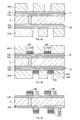
- FIG. 4A is a schematic cross-sectional view showing the next step of FIG. 3
- FIG. 4B is a schematic cross-sectional view showing the next step of FIG. 4A
- FIG. 4C is the next step of FIG. 4B.
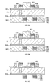
- 5A is a schematic cross-sectional view showing the next step of FIG. 4C
- FIG. 5B is a schematic cross-sectional view showing the next step of FIG. 5A
- FIG. 5C is the next step of FIG. 5B.
- FIG. 6A is a schematic cross-sectional view showing the next step of FIG. 5C
- FIG. 6B is a schematic cross-sectional view showing the next step of FIG. 6A
- FIG. 6C is the next step of FIG. 6B.
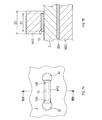
- 7A is a schematic partial enlarged plan view of the periphery of the auxiliary wiring in the process of FIG. 6A
- FIG. 7B is a schematic partial cross-sectional view taken along the line VIIB-VIIB of FIG. 7A
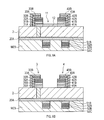
- 8A is a schematic cross-sectional view showing the next step of FIG. 6C
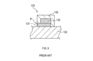
- FIG. 8B is a schematic cross-sectional view showing the next step of FIG. 8A. It is typical sectional drawing of the conventional wiring board.
- DESCRIPTION OF SYMBOLS 1 ... Wiring board, 2 ... Insulating layer, 3 ... 1st wiring part, 4 ... 2nd wiring part, 5 ... 3rd wiring part, 6 ... Via conductor, 10 ... Surface side lower-treatment layer, DESCRIPTION OF SYMBOLS 11 ... Base pattern, 12 ... Auxiliary wiring, 13A, 13B ... Connection part, 20 ... Back side lower treatment layer, 31 ... Conductive underlayer, 32 ... Conductive layer, 33 ... conductive coating layer, 41 ... conductive base layer, 42 ... conductive layer, 43 ... conductive coating layer, 51 ... conductive base layer, 52 ... conductive layer, M10, M11, M12, M20, M21, M22, M23... Mask layer.
- a wiring board 1 shown in FIG. 1 includes an insulating layer 2 having a front surface and a back surface, a first wiring portion 3, a second wiring portion 4, a third wiring portion 5, and a via conductor 6.
- the insulating layer 2 is a ceramic sheet-like member.
- the ceramic constituting the insulating layer 2 include alumina, beryllia, aluminum nitride, boron nitride, silicon nitride, and glass. These ceramics can be used alone or in combination of two or more.
- the first wiring part 3 and the second wiring part 4 are each disposed on the surface of the insulating layer 2.
- the first wiring part 3 and the second wiring part 4 are insulated from each other.
- the first wiring part 3 is electrically connected to the third wiring part 5 by a via conductor 6.
- the first wiring unit 3 is electrically connected to an external terminal via the third wiring unit 5.
- the second wiring portion 4 is not electrically connected to other wiring portions and is electrically independent in the insulating layer 2.
- the first wiring part 3 includes a conductive base layer 31, a conductive layer 32, and a conductive coating layer 33.
- the conductive base layer 31, the conductive layer 32, and the conductive coating layer 33 each have a two-layer structure.
- the conductive base layer 31 includes a first conductive base layer 31A and a second conductive base layer 31B.
- the conductive layer 32 includes a first conductive layer 32A and a second conductive layer 32B.
- the conductive coating layer 33 includes a first conductive coating layer 33A and a second conductive coating layer 33B.
- the second wiring portion 4 includes a conductive base layer 41, a conductive layer 42, and a conductive coating layer 43.
- the conductive base layer 41, the conductive layer 42, and the conductive coating layer 43 each have a two-layer structure.
- the conductive base layer 41 includes a first conductive base layer 41A and a second conductive base layer 41B.
- the conductive layer 42 includes a first conductive layer 42A and a second conductive layer 42B.
- the conductive coating layer 43 includes a first conductive coating layer 43A and a second conductive coating layer 43B.
- the first wiring part 3 Since the plurality of layers constituting the second wiring part 4 have the same configuration (for example, material and arrangement) as the plurality of layers constituting the first wiring part 3, the first wiring part 3 is configured below. A plurality of layers will be described.
- the conductive base layer 31 includes a first conductive base layer 31A disposed on the surface of the insulating layer 2 and a second conductive base layer 31B disposed on the surface of the first conductive base layer 31A.
- the first conductive base layer 31A and the second conductive base layer 31B have the same shape in plan view (that is, viewed from the thickness direction).
- the first conductive base layer 31A of the first wiring part 3 is connected to the via conductor 6, but the first conductive base layer 41A of the second wiring part 4 is not connected to the via conductor.
- the material of the conductive base layer 31 is not particularly limited as long as it has conductivity.
- the material of the first conductive base layer 31A can be titanium (Ti), and the material of the second conductive base layer 31B can be copper (Cu).
- the conductive layer 32 includes a first conductive layer 32A disposed on the surface of the second conductive base layer 31B, and a second conductive layer 32B disposed on the surface of the first conductive layer 32A.
- the first conductive layer 32A and the second conductive layer 32B have the same shape in plan view.
- the material of the conductive layer 32 is not particularly limited as long as it has conductivity.
- the material of the first conductive layer 32A can be copper (Cu), and the material of the second conductive layer 32B can be nickel (Ni).
- the second conductive base layer 31B which is the outermost surface layer on the surface side of the conductive base layer 31, and the first conductive layer 32A in contact with the second conductive base layer 31B of the conductive layer 32 are the same type of metal ( For example, copper) may be included. Thereby, the adhesion degree of the conductive base layer 31 and the conductive layer 32 can be increased.
- the conductive base layer 31 overlaps with the conductive layer 32 in plan view, and does not protrude outside the conductive layer 32. That is, the entire surface of the second conductive base layer 31B is covered with the first conductive layer 32A.
- the conductive coating layer 33 is disposed so as to cover part of the surface of the conductive layer 32, part of the side surface of the conductive base layer 31, and part of the side surface of the conductive layer 32.
- the conductive coating layer 33 is a portion of the surface of the second conductive layer 32 ⁇ / b> B, the side surface of the conductive base layer 31, and the side surface of the conductive layer 32 that is far from the second wiring portion 4. In other words, it is arranged so as to cover (the portion not facing the second wiring portion 4).
- the conductive coating layer 33 is in contact with only the side surface of the conductive underlayer 31, and Does not touch the surface.
- the conductive layer 32 and The overlapping part has the same shape.
- the material of the conductive coating layer 33 is not particularly limited as long as it has conductivity.
- the material of the first conductive coating layer 33A can be nickel (Ni), and the material of the second conductive coating layer 33B can be gold (Au).
- the second conductive layer 32B that is the outermost layer on the surface side of the conductive layer 32 and the first conductive coating layer 33A that is the outermost layer in contact with the second conductive layer 32B of the conductive coating layer 33 are of the same type. It is good to contain a metal (for example, nickel). Thereby, the adhesion degree of the conductive layer 32 and the conductive coating layer 33 can be increased.
- the uncovered regions that are not covered with the conductive coating layers 33 and 43 are covered with an oxide film. It has been broken.
- the non-covering region among the surface and side surfaces of the conductive layers 32, 42, the conductive coating layer 33, the region not covered with the conductive coating layers 33, 43, and the conductive coating layer among the side surfaces of the conductive base layers 31, 41.
- cover is included.
- the oxide film is mainly composed of metal oxides contained in the conductive layers 32 and 42 and the conductive base layers 31 and 41.
- the oxide film has a thickness of several to several tens of millimeters, for example, 10 inches.
- the oxide film is formed on the conductive layers 32 and 42 and the conductive underlayers 31 and 41 by heating the wiring substrate 1 in the air atmosphere (that is, annealing treatment). Note that regions of the surfaces and side surfaces of the conductive coating layers 33 and 43 that are not in contact with the conductive layers 32 and 42 and the conductive base layers 31 and 41 may be covered with an oxide film.
- the third wiring portion 5 is disposed on the back surface of the insulating layer 2.
- the third wiring unit 5 includes a conductive base layer 51 and a plurality of conductive layers 52.
- the conductive base layer 51 is disposed on the back surface of the insulating layer 2 and has a two-layer structure.
- the conductive base layer 51 includes a first conductive base layer 51A disposed on the back surface of the insulating layer 2 and a plurality of second conductive base layers 51B disposed separately on the back surface of the first conductive base layer 51A. And have.
- the first conductive base layer 51 ⁇ / b> A is connected to the via conductor 6.
- the “back surface” in the third wiring portion 5 means a surface on the opposite side to the insulating layer 2.
- the material of the conductive base layer 51 is not particularly limited as long as it has conductivity.
- the material of the first conductive base layer 51A can be titanium (Ti), and the material of the second conductive base layer 51B can be copper (Cu).
- the plurality of conductive layers 52 are respectively disposed on the back surfaces of the plurality of second conductive base layers 51B and have a three-layer structure.
- Each conductive layer 52 includes a first conductive layer 52A disposed on the back surface of the second conductive base layer 51B, a second conductive layer 52B disposed on the back surface of the first conductive layer 52A, and the second conductive layer 52B. And a third conductive layer 52C disposed on the back surface.
- the first conductive layer 52A, the second conductive layer 52B, and the third conductive layer 52C have the same shape in plan view.
- the material of the conductive layer 52 is not particularly limited as long as it has conductivity.
- the material of the first conductive layer 52A can be copper (Cu)
- the material of the second conductive layer 52B can be nickel (Ni)
- the material of the third conductive layer 52C can be gold (Au).
- the via conductor 6 is a conductor that penetrates the insulating layer 2 in the thickness direction.
- the via conductor 6 electrically connects the first wiring part 3 and the third wiring part 5.
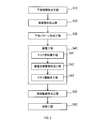
- the manufacturing method of the wiring board according to the present embodiment includes an undertreatment layer forming step S10, a conductive layer forming step S20, a base pattern forming step S30, a covering step S40, and an auxiliary wiring removing step S50. And a heating step S60.
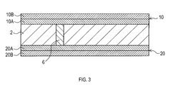
- a conductive surface-side lower treatment layer 10 having a two-layer structure is formed on the surface of the insulating layer 2 provided with the via conductors 6.
- a conductive back side lower treatment layer 20 having a two-layer structure is also formed on the back side of the insulating layer 2.
- the surface side lower treatment layer 10 includes portions that become the conductive base layer 31 of the first wiring part 3 and the conductive base layer 41 of the second wiring part 4.
- the back side lower treatment layer 20 includes a portion that becomes the conductive base layer 51 of the third wiring portion 5.
- the front side lower treatment layer 10 and the rear side lower treatment layer 20 can be formed by, for example, metal sputtering. Specifically, the first surface side lower treatment layer 10A and the first rear surface side lower treatment layer 20A are formed on the front and back surfaces of the insulating layer 2 by Ti sputtering, and further, the second surface side lower treatment layer is formed by Cu sputtering. 10B and the 2nd back surface side lower process layer 20B are accumulated and formed.
- the conductive layer 32 constituting the first wiring part 3 and the conductive layer 42 constituting the second wiring part 4 are formed on the surface of the second surface side lower treatment layer 10B.
- the conductive layer 52 constituting the third wiring portion 5 is formed on the back surface of the second back surface side lower treatment layer 20B.
- the mask layer M10 is arranged on the surface of the second front surface side lower treatment layer 10B, and the mask layer M20 is arranged on the rear surface of the second rear surface side lower treatment layer 20B.
- the mask layers M10 and M20 are configured to cover a portion of the lower processing layer where the conductive layer is not formed.
- the mask layers M10 and M20 are formed of a resist, for example.
- electroplating is performed a plurality of times on the front surface side and the back surface side of the insulating layer 2, respectively. Thereby, the conductive layer 32 of the first wiring part 3, the conductive layer 42 of the second wiring part 4, and the conductive layer 52 of the third wiring part 5 are formed. In the electroplating in this step, electricity is conducted to the formation portion of the second wiring portion 4 by the surface side lower treatment layer 10 and the conductive layer 42 is formed.
- the resist is removed as shown in FIG. 4C, and the second surface side lower treatment layer 10B and the second back side lower treatment layer 20B are etched using the conductive layer as a mask. Thereby, the second conductive base layer 31B of the first wiring part 3, the second conductive base layer 41B of the second wiring part 4, and the second conductive base layer 51B of the third wiring part 5 are formed.
- a mask layer M11 is disposed so as to cover a portion of the first surface side lower treatment layer 10A where the auxiliary wiring 12 is to be formed. At the same time, the entire back surface side of the insulating layer 2 is covered with the mask layer M21.
- portions of the first surface-side lower treatment layer 10A that are not covered with the mask layer M11 and the two conductive layers 32 and 42 are removed by etching. Thereby, the base pattern 11 including the auxiliary wiring 12 is formed. After the base pattern 11 is formed, the mask layers M11 and M21 are removed as shown in FIG. 5C.
- the conductive coating layers 33 and 43 are respectively coated on the surfaces of the conductive layer 32 of the first wiring portion 3 and the conductive layer 42 of the second wiring portion 4.
- This step includes a mask layer arranging step S41, a conductive coating layer forming step S42, and a mask layer removing step S43.
- a mask layer M12 that covers the base pattern 11 is disposed.
- the entire back surface side of the insulating layer 2 is covered with the mask layer M22.
- the mask layer M12 is configured to cover a region of the base pattern 11 where the conductive coating layers 33 and 43 are not formed. Specifically, as shown in FIG. 7A, the mask layer M12 includes the entire surface of the auxiliary wiring 12 in the base pattern 11, and the first conductive base layer 31A (in FIG. 7A, conductive). 13A) and the auxiliary wiring 12 and the first conductive base layer 41A of the second wiring portion 4 (which overlaps the conductive layer 42 in FIG. 7A) and the auxiliary wiring 12 It arrange
- the mask layer M12 is disposed so as to cover part of the surfaces of the conductive layer 32 of the first wiring part 3 and the conductive layer 42 of the second wiring part 4.
- the mask layer M ⁇ b> 12 includes a portion of the side surface of the conductive layer 32 of the first wiring unit 3 and the side surface of the conductive layer 42 of the second wiring unit 4 that face each other and the second conductive base layer of the first wiring unit 3. It arrange
- the mask layer M12 is disposed so as to cover the entire side surface of the auxiliary wiring 12 between the conductive layer 32 of the first wiring part 3 and the conductive layer 42 of the second wiring part 4. .
- the width D2 of the mask layer M12 in the direction perpendicular to the side surface of the auxiliary wiring 12 is preferably 1.2 times or more, more preferably 1.5 times or more the width D1 of the auxiliary wiring 12.
- the conductive coating layer 33 of the first wiring part 3 and the conductive coating layer 43 of the second wiring part 4 are formed by electrolytic plating in a state where the mask layers M12 and M22 are arranged. To do.
- electricity is conducted to the portion where the second wiring portion 4 is formed by the auxiliary wiring 12, and the conductive coating layer 43 is formed.
- auxiliary wiring removal process In this step, the auxiliary wiring 12 is removed. Specifically, first, as shown in FIG. 8A, the entire back surface side of the insulating layer 2 is covered with a mask layer M23.
- the auxiliary wiring 12 is removed by etching using the conductive coating layers 33 and 43 as a mask. Thereby, the first conductive base layer 31A of the first wiring part 3 and the first conductive base layer 41A of the second wiring part 4 are separated, and the first wiring part 3 and the second wiring part 4 which are insulated from each other are separated. It is formed. After removing the auxiliary wiring 12, the mask layer M23 is removed.
- the heating temperature in this step is, for example, 250 ° C. or higher and 350 ° C. or lower.
- an oxide film is formed on the exposed surfaces of the conductive layers 32 and 42, the conductive base layers 31 and 41, and the conductive coating layers 33 and 43, and the wiring substrate 1 of FIG. 1 is obtained.
- the conductive coating layers 33 and 43 are suppressed from being directly disposed on the conductive base layers 31 and 41. Therefore, the occurrence of undercut in the mask layer removing step S43 is suppressed, and the adhesion strength of the conductive coating layers 33 and 43 is improved. As a result, a high-quality wiring board including an electrically independent wiring portion can be obtained.
- the side surface of the auxiliary wiring 12 is covered with the mask layer M12, so that a plating layer that becomes a plating foreign substance is formed in a region adjacent to the side surface of the auxiliary wiring 12. Can be suppressed. As a result, the quality of the wiring board can be improved.
- the mask layer M12 is disposed so as to cover a part of the surface of the conductive layers 32 and 42, so that the conductive underlayer 31 and It is possible to prevent the conductive coating layers 33 and 43 from being directly disposed on the 41. In addition, since the accuracy required for the shape of the mask layer M12 can be reduced, the production of the wiring board is facilitated.
- the mask layer M12 in the covering step S40 is disposed so as to cover the connecting portions 13A and 13B between the two conductive base layers 31 and 41 and the auxiliary wiring 12. For example, it is not always necessary to cover the side surface of the auxiliary wiring 12.
- the mask layer M12 in the covering step S40 is arranged so as to cover the side surface of the auxiliary wiring 12, it is necessary to cover the connecting portions 13A and 13B between the two conductive base layers 31 and 41 and the auxiliary wiring 12. There is no.
- the mask layer M12 in the coating step S40 does not cover the surfaces of the conductive layers 32 and 42 and does not contact the side surfaces of the two conductive base layers 31 and 41.
- the surface and side surfaces of the auxiliary wiring 12 may be covered (that is, separated from the side surfaces of the two conductive base layers 31 and 41).
- the mask layer M12 covers the connecting portions 13A and 13B between the two conductive base layers 31 and 41 and the auxiliary wiring 12, or covers the side surfaces of the auxiliary wiring 12, the quality of the wiring board 1 is improved. can do.
- the material of the insulating layer 2 is not limited to ceramic.
- the insulating layer 2 may be made of resin.
- the wiring portion may not be provided on the back surface of the insulating layer 2. That is, the wiring board 1 may be a single-sided board. Further, the wiring substrate 1 may have three or more wiring portions insulated from each other on the surface of the insulating layer 2.
- the conductive coating layers 33 and 43 may cover the entire surfaces of the conductive layers 32 and 42 and portions of the side surfaces of the conductive layers 32 and 42 that face each other. That is, in the method for manufacturing a wiring board according to the above embodiment, the mask layer M12 in the covering step S40 does not cover the surfaces of the conductive layers 32 and 42, and the side surfaces of the two conductive base layers 31 and 41 and the auxiliary wiring 12 are covered. It may be arranged so as to cover the surface.
- the structure of the layers constituting each wiring part is an example. That is, the conductive base layers 31 and 41, the conductive layers 32 and 42, and the conductive coating layers 33 and 43 may have a single-layer structure or a multilayer structure of three or more layers.
- the uncovered regions of the conductive layers 32 and 42 and the conductive base layers 31 and 41 do not necessarily have to be covered with an oxide film. That is, the heating step S60 may be omitted in the method for manufacturing a wiring board according to the embodiment.
Landscapes
- Engineering & Computer Science (AREA)
- Microelectronics & Electronic Packaging (AREA)
- Manufacturing & Machinery (AREA)
- Manufacturing Of Printed Wiring (AREA)
- Production Of Multi-Layered Print Wiring Board (AREA)
Abstract
Description
導電性被覆層を形成する電解メッキにおいて、補助配線の表面のみをマスク層で被覆すると、補助配線の側面にメッキ層が形成され得る。このメッキ層は、補助配線を除去する工程においても除去されずに残存し、メッキ異物となるおそれがある。
5…第3配線部、6…ビア導体、10…表面側下処理層、
11…下地パターン、12…補助配線、13A,13B…連結部分、
20…裏面側下処理層、31…導電性下地層、32…導電層、
33…導電性被覆層、41…導電性下地層、42…導電層、
43…導電性被覆層、51…導電性下地層、52…導電層、
M10,M11,M12,M20,M21,M22,M23…マスク層。
[1.第1実施形態]
[1-1.配線基板]
図1に示す配線基板1は、表面及び裏面を有する絶縁層2と、第1配線部3と、第2配線部4と、第3配線部5と、ビア導体6とを備える。
絶縁層2は、セラミック製のシート状の部材である。絶縁層2を構成するセラミックとしては、例えばアルミナ、ベリリア、窒化アルミニウム、窒化ホウ素、窒化ケイ素、ガラス等が挙げられる。これらのセラミックは単体で、又は2種以上組み合わせて使用することができる。
第1配線部3及び第2配線部4は、それぞれ、絶縁層2の表面に配置されている。第1配線部3と第2配線部4とは、互いに絶縁されている。
導電性下地層31は、絶縁層2の表面に配置された第1導電性下地層31Aと、第1導電性下地層31Aの表面に配置された第2導電性下地層31Bとを有する。第1導電性下地層31Aと第2導電性下地層31Bとは、平面視で(つまり厚み方向から視て)同形状である。なお、第1配線部3の第1導電性下地層31Aは、ビア導体6に接続されているが、第2配線部4の第1導電性下地層41Aは、ビア導体に接続されていない。
導電層32は、第2導電性下地層31Bの表面に配置された第1導電層32Aと、第1導電層32Aの表面に配置された第2導電層32Bとを有する。第1導電層32Aと第2導電層32Bとは、平面視で同形状である。
導電性被覆層33は、導電層32の表面の一部と、導電性下地層31の側面の一部及び導電層32の側面の一部とを覆うように配置されている。
第3配線部5は、絶縁層2の裏面に配置される。第3配線部5は、導電性下地層51と、複数の導電層52とを有する。
ビア導体6は、絶縁層2を厚み方向に貫通する導体である。ビア導体6は、第1配線部3と第3配線部5とを電気的に接続する。
次に、配線基板1の製造方法について説明する。
本実施形態の配線基板の製造方法は、図2に示すように、下処理層形成工程S10と、導電層形成工程S20と、下地パターン形成工程S30と、被覆工程S40と、補助配線除去工程S50と、加熱工程S60とを備える。
本工程では、図3に示すように、ビア導体6を設けた絶縁層2の表面に、2層構造の導電性の表面側下処理層10を形成する。また、同時に、絶縁層2の裏面にも2層構造の導電性の裏面側下処理層20を形成する。
本工程では、第2表面側下処理層10Bの表面に第1配線部3を構成する導電層32と、第2配線部4を構成する導電層42とを形成する。また、同時に、第2裏面側下処理層20Bの裏面に第3配線部5を構成する導電層52を形成する。
本工程では、第1表面側下処理層10Aのエッチングにより、導電層32がその表面に配置された導電性下地層31、及び導電層42がその表面に配置された導電性下地層41と、導電性下地層31,41同士を接続する補助配線12とを含む下地パターン11を形成する。
本工程では、第1配線部3の導電層32及び第2配線部4の導電層42の表面にそれぞれ導電性被覆層33,43を被覆する。本工程は、マスク層配置工程S41と、導電性被覆層形成工程S42と、マスク層除去工程S43とを有する。
本工程では、図6Aに示すように、下地パターン11を覆うマスク層M12を配置する。また、本工程では、絶縁層2の裏面側全体をマスク層M22で覆う。
本工程では、図6Bに示すように、マスク層M12,M22を配置した状態で、電解メッキによって第1配線部3の導電性被覆層33及び第2配線部4の導電性被覆層43を形成する。なお、本工程の電気メッキでは、補助配線12によって、第2配線部4の形成部分に電気が導通され、導電性被覆層43が形成される。
本工程では、図6Cに示すように、マスク層M12,M22を除去する。この状態では、第1配線部3及び第2配線部4は補助配線12によって導通されている。
本工程では、補助配線12を除去する。具体的には、まず、図8Aに示すように、絶縁層2の裏面側全体をマスク層M23で覆う。
本工程では、補助配線12を除去した後、導電層32,42及び導電性下地層31,41を含む基板全体に対し、大気雰囲気下で加熱するアニール処理を行う。
以上詳述した実施形態によれば、以下の効果が得られる。
(1a)導電性下地層31,41が、平面視で導電層32,42と一致するように重なっているため、導電性下地層31,41に導電性被覆層33,43が直接配置されることが抑制される。
以上、本開示の実施形態について説明したが、本開示は、上記実施形態に限定されることなく、種々の形態を採り得ることは言うまでもない。
(2c)上記実施形態の配線基板1において、絶縁層2の裏面に配線部が設けられなくてもよい。つまり、配線基板1は、片面基板であってもよい。また、配線基板1は、絶縁層2の表面に互いに絶縁された3以上の配線部を有してもよい。
Claims (9)
- 表面及び裏面を有する絶縁層と、
前記絶縁層の少なくとも表面に配置され、互いに絶縁された少なくとも2つの配線部と、
を備え、
前記少なくとも2つの配線部のうち、少なくとも1つの配線部は前記絶縁層において電気的に独立し、
前記少なくとも2つの配線部は、それぞれ、
前記絶縁層の表面に配置された導電性下地層と、
前記導電性下地層の表面に配置された導電層と、
前記導電層の表面の少なくとも一部と前記導電性下地層の側面の少なくとも一部及び前記導電層の側面の少なくとも一部とを覆うように配置された導電性被覆層と、
を有し、
前記導電性下地層は、平面視で前記導電層と一致するように重なっている、配線基板。 - 前記導電層のうち表面側の最表層と、前記導電性被覆層のうち前記導電層と当接する最表層とは、同種の金属を含む、請求項1に記載の配線基板。
- 前記導電層及び前記導電性下地層において前記導電性被覆層に覆われていない非被覆領域は、酸化物膜で覆われている、請求項1又は請求項2に記載の配線基板。
- 表面及び裏面を有する絶縁層と、前記絶縁層の少なくとも表面に配置され、互いに絶縁された少なくとも2つの配線部とを備え、前記少なくとも2つの配線部のうち、少なくとも1つの配線部は前記絶縁層において電気的に独立した配線基板の製造方法であって、
前記絶縁層の表面に、導電性の下処理層を形成する工程と、
前記下処理層の表面に少なくとも2つの導電層を形成する工程と、
前記下処理層のエッチングにより、前記少なくとも2つの導電層がそれぞれその表面に配置された少なくとも2つの導電性下地層と、前記少なくとも2つの導電性下地層同士を接続する補助配線とを含む下地パターンを形成する工程と、
前記少なくとも2つの導電層の表面にそれぞれ導電性被覆層を被覆する工程と、
前記補助配線を除去する工程と、
を備え、
前記被覆する工程は、
前記下地パターンを覆うマスク層を配置する工程と、
前記マスク層を配置した状態で、電解メッキによって前記導電性被覆層を形成する工程と、
前記マスク層を除去する工程と、
を有し、
前記マスク層を配置する工程で、前記マスク層は、前記下地パターンのうち、前記少なくとも2つの導電性下地層と前記補助配線との連結部分を覆うように配置される、配線基板の製造方法。 - 前記マスク層を配置する工程で、前記マスク層は、前記補助配線の側面を覆うように配置される、請求項4に記載の配線基板の製造方法。
- 前記マスク層を配置する工程で、前記マスク層は、前記少なくとも2つの導電層の表面の一部を覆うように配置される、請求項4又は請求項5に記載の配線基板の製造方法。
- 前記補助配線を除去する工程の後、前記少なくとも2つの導電層及び前記少なくとも2つの導電性下地層を大気雰囲気下で加熱する工程をさらに備える、請求項4から請求項6のいずれか1項に記載の配線基板の製造方法。
- 表面及び裏面を有する絶縁層と、前記絶縁層の少なくとも表面に配置され、互いに絶縁された少なくとも2つの配線部とを備え、前記少なくとも2つの配線部のうち、少なくとも1つの配線部は前記絶縁層において電気的に独立した配線基板の製造方法であって、
前記絶縁層の表面に、導電性の下処理層を形成する工程と、
前記下処理層の表面に少なくとも2つの導電層を形成する工程と、
前記下処理層のエッチングにより、前記少なくとも2つの導電層がそれぞれその表面に配置された少なくとも2つの導電性下地層と、前記少なくとも2つの導電性下地層同士を接続する補助配線とを含む下地パターンを形成する工程と、
前記少なくとも2つの導電層の表面にそれぞれ導電性被覆層を被覆する工程と、
前記補助配線を除去する工程と、
を備え、
前記被覆する工程は、
前記下地パターンを覆うマスク層を配置する工程と、
前記マスク層を配置した状態で、電解メッキによって前記導電性被覆層を形成する工程と、
前記マスク層を除去する工程と、
を有し、
前記マスク層を配置する工程で、前記マスク層は、前記補助配線の側面を覆うように配置される、配線基板の製造方法。 - 前記補助配線を除去する工程の後、前記少なくとも2つの導電層及び前記少なくとも2つの導電性下地層を大気雰囲気下で加熱する工程をさらに備える、請求項8に記載の配線基板の製造方法。
Priority Applications (3)
| Application Number | Priority Date | Filing Date | Title |
|---|---|---|---|
| KR1020197034748A KR20190141230A (ko) | 2017-06-07 | 2018-05-28 | 배선 기판, 및 배선 기판의 제조 방법 |
| US16/618,606 US11272623B2 (en) | 2017-06-07 | 2018-05-28 | Wiring substrate and method for producing wiring substrate |
| JP2019523459A JP6989603B2 (ja) | 2017-06-07 | 2018-05-28 | 配線基板、及び配線基板の製造方法 |
Applications Claiming Priority (2)
| Application Number | Priority Date | Filing Date | Title |
|---|---|---|---|
| JP2017112643 | 2017-06-07 | ||
| JP2017-112643 | 2017-06-07 |
Publications (1)
| Publication Number | Publication Date |
|---|---|
| WO2018225555A1 true WO2018225555A1 (ja) | 2018-12-13 |
Family
ID=64566270
Family Applications (1)
| Application Number | Title | Priority Date | Filing Date |
|---|---|---|---|
| PCT/JP2018/020313 Ceased WO2018225555A1 (ja) | 2017-06-07 | 2018-05-28 | 配線基板、及び配線基板の製造方法 |
Country Status (5)
| Country | Link |
|---|---|
| US (1) | US11272623B2 (ja) |
| JP (1) | JP6989603B2 (ja) |
| KR (1) | KR20190141230A (ja) |
| TW (1) | TWI739008B (ja) |
| WO (1) | WO2018225555A1 (ja) |
Cited By (1)
| Publication number | Priority date | Publication date | Assignee | Title |
|---|---|---|---|---|
| JP2025127549A (ja) * | 2024-02-21 | 2025-09-02 | 日本特殊陶業株式会社 | 配線基板 |
Citations (5)
| Publication number | Priority date | Publication date | Assignee | Title |
|---|---|---|---|---|
| JPS5013881A (ja) * | 1973-06-11 | 1975-02-13 | ||
| JPH0575258A (ja) * | 1991-09-11 | 1993-03-26 | Fujitsu Ltd | プリント配線板の製造方法 |
| JP2001068828A (ja) * | 1999-08-27 | 2001-03-16 | Ngk Spark Plug Co Ltd | 配線基板及びその製造方法 |
| JP2003224348A (ja) * | 2002-01-31 | 2003-08-08 | Toppan Printing Co Ltd | 高密度プリント配線板及びその製造方法 |
| JP2009212212A (ja) * | 2008-03-03 | 2009-09-17 | Shinko Seisakusho:Kk | 回路基板の製造方法 |
Family Cites Families (6)
| Publication number | Priority date | Publication date | Assignee | Title |
|---|---|---|---|---|
| JPS56118209A (en) * | 1980-02-20 | 1981-09-17 | Hitachi Ltd | Conductor |
| US5071518A (en) * | 1989-10-24 | 1991-12-10 | Microelectronics And Computer Technology Corporation | Method of making an electrical multilayer interconnect |
| JP4081052B2 (ja) * | 2003-12-05 | 2008-04-23 | 三井金属鉱業株式会社 | プリント配線基板の製造法 |
| JP2008243853A (ja) * | 2007-03-23 | 2008-10-09 | Renesas Technology Corp | インターポーザ基板、それを利用したlsiチップ及び情報端末装置、インターポーザ基板製造方法、並びにlsiチップ製造方法 |
| JP5781877B2 (ja) | 2011-09-22 | 2015-09-24 | 日本特殊陶業株式会社 | 配線基板の製造方法 |
| JP6324876B2 (ja) * | 2014-07-16 | 2018-05-16 | 新光電気工業株式会社 | 配線基板、半導体装置及び配線基板の製造方法 |
-
2018
- 2018-05-28 WO PCT/JP2018/020313 patent/WO2018225555A1/ja not_active Ceased
- 2018-05-28 JP JP2019523459A patent/JP6989603B2/ja active Active
- 2018-05-28 US US16/618,606 patent/US11272623B2/en active Active
- 2018-05-28 KR KR1020197034748A patent/KR20190141230A/ko not_active Ceased
- 2018-06-04 TW TW107119117A patent/TWI739008B/zh active
Patent Citations (5)
| Publication number | Priority date | Publication date | Assignee | Title |
|---|---|---|---|---|
| JPS5013881A (ja) * | 1973-06-11 | 1975-02-13 | ||
| JPH0575258A (ja) * | 1991-09-11 | 1993-03-26 | Fujitsu Ltd | プリント配線板の製造方法 |
| JP2001068828A (ja) * | 1999-08-27 | 2001-03-16 | Ngk Spark Plug Co Ltd | 配線基板及びその製造方法 |
| JP2003224348A (ja) * | 2002-01-31 | 2003-08-08 | Toppan Printing Co Ltd | 高密度プリント配線板及びその製造方法 |
| JP2009212212A (ja) * | 2008-03-03 | 2009-09-17 | Shinko Seisakusho:Kk | 回路基板の製造方法 |
Cited By (1)
| Publication number | Priority date | Publication date | Assignee | Title |
|---|---|---|---|---|
| JP2025127549A (ja) * | 2024-02-21 | 2025-09-02 | 日本特殊陶業株式会社 | 配線基板 |
Also Published As
| Publication number | Publication date |
|---|---|
| TWI739008B (zh) | 2021-09-11 |
| JPWO2018225555A1 (ja) | 2019-07-25 |
| JP6989603B2 (ja) | 2022-01-05 |
| KR20190141230A (ko) | 2019-12-23 |
| US20200196455A1 (en) | 2020-06-18 |
| TW201906506A (zh) | 2019-02-01 |
| US11272623B2 (en) | 2022-03-08 |
Similar Documents
| Publication | Publication Date | Title |
|---|---|---|
| US20240015884A1 (en) | Wiring circuit board and method for producing wiring circuit board | |
| JP7457923B2 (ja) | 実装基板及びその製造方法 | |
| US12114438B2 (en) | Manufacturing method for double-sided wiring circuit board and double-sided wiring circuit board | |
| JPWO2018159023A1 (ja) | フレキシブルプリント配線板、接続体の製造方法及び接続体 | |
| TW200950633A (en) | Flex-rigid wiring board and method for manufacturing the same | |
| TW202014070A (zh) | 復合電路板及其製造方法 | |
| JP5781877B2 (ja) | 配線基板の製造方法 | |
| JP5651933B2 (ja) | サスペンション用基板およびその製造方法 | |
| TWI377890B (ja) | ||
| JP6989603B2 (ja) | 配線基板、及び配線基板の製造方法 | |
| TWI900581B (zh) | 配線電路基板 | |
| JP2018148086A (ja) | 貫通電極基板の製造方法及び貫通電極基板 | |
| JP2006128291A (ja) | 多層プリント配線板の製造方法、多層プリント配線板及び電子装置 | |
| CN104703401A (zh) | 一种电路板的电镀方法 | |
| JP2010109044A (ja) | 配線基板及びこれを用いたプローブカード | |
| TWI385765B (zh) | 內埋式線路結構及其製作方法 | |
| JP2010129730A (ja) | 配線基板及びこれを用いたプローブカード | |
| JPH09270355A (ja) | 電子部品及びその製造方法 | |
| US20110269307A1 (en) | Method for Making Integrated Circuit Device Using Copper Metallization on 1-3 PZT Composite | |
| JPH0621651A (ja) | 多層配線回路板及びその製造方法 | |
| JP4196320B2 (ja) | 薄膜付実装回路樹脂基板 | |
| KR20230110264A (ko) | 배선 회로 기판 | |
| TW202549430A (zh) | 配線電路基板 | |
| JP4755454B2 (ja) | プリント基板の製造方法 | |
| TWI419033B (zh) | Method for manufacturing two - layer circuit board structure for capacitive touch panel |
Legal Events
| Date | Code | Title | Description |
|---|---|---|---|
| 121 | Ep: the epo has been informed by wipo that ep was designated in this application |
Ref document number: 18813888 Country of ref document: EP Kind code of ref document: A1 |
|
| ENP | Entry into the national phase |
Ref document number: 2019523459 Country of ref document: JP Kind code of ref document: A |
|
| ENP | Entry into the national phase |
Ref document number: 20197034748 Country of ref document: KR Kind code of ref document: A |
|
| NENP | Non-entry into the national phase |
Ref country code: DE |
|
| 122 | Ep: pct application non-entry in european phase |
Ref document number: 18813888 Country of ref document: EP Kind code of ref document: A1 |