WO2018221317A1 - 発光装置およびプロジェクター - Google Patents
発光装置およびプロジェクター Download PDFInfo
- Publication number
- WO2018221317A1 WO2018221317A1 PCT/JP2018/019641 JP2018019641W WO2018221317A1 WO 2018221317 A1 WO2018221317 A1 WO 2018221317A1 JP 2018019641 W JP2018019641 W JP 2018019641W WO 2018221317 A1 WO2018221317 A1 WO 2018221317A1
- Authority
- WO
- WIPO (PCT)
- Prior art keywords
- light
- emitting device
- light emitting
- flat plate
- phosphor
- Prior art date
- Legal status (The legal status is an assumption and is not a legal conclusion. Google has not performed a legal analysis and makes no representation as to the accuracy of the status listed.)
- Ceased
Links
Images


Classifications
-
- G—PHYSICS
- G03—PHOTOGRAPHY; CINEMATOGRAPHY; ANALOGOUS TECHNIQUES USING WAVES OTHER THAN OPTICAL WAVES; ELECTROGRAPHY; HOLOGRAPHY
- G03B—APPARATUS OR ARRANGEMENTS FOR TAKING PHOTOGRAPHS OR FOR PROJECTING OR VIEWING THEM; APPARATUS OR ARRANGEMENTS EMPLOYING ANALOGOUS TECHNIQUES USING WAVES OTHER THAN OPTICAL WAVES; ACCESSORIES THEREFOR
- G03B21/00—Projectors or projection-type viewers; Accessories therefor
- G03B21/14—Details
- G03B21/20—Lamp housings
- G03B21/2006—Lamp housings characterised by the light source
- G03B21/2033—LED or laser light sources
- G03B21/204—LED or laser light sources using secondary light emission, e.g. luminescence or fluorescence
-
- F—MECHANICAL ENGINEERING; LIGHTING; HEATING; WEAPONS; BLASTING
- F21—LIGHTING
- F21V—FUNCTIONAL FEATURES OR DETAILS OF LIGHTING DEVICES OR SYSTEMS THEREOF; STRUCTURAL COMBINATIONS OF LIGHTING DEVICES WITH OTHER ARTICLES, NOT OTHERWISE PROVIDED FOR
- F21V7/00—Reflectors for light sources
- F21V7/22—Reflectors for light sources characterised by materials, surface treatments or coatings, e.g. dichroic reflectors
- F21V7/28—Reflectors for light sources characterised by materials, surface treatments or coatings, e.g. dichroic reflectors characterised by coatings
- F21V7/30—Reflectors for light sources characterised by materials, surface treatments or coatings, e.g. dichroic reflectors characterised by coatings the coatings comprising photoluminescent substances
-
- F—MECHANICAL ENGINEERING; LIGHTING; HEATING; WEAPONS; BLASTING
- F21—LIGHTING
- F21V—FUNCTIONAL FEATURES OR DETAILS OF LIGHTING DEVICES OR SYSTEMS THEREOF; STRUCTURAL COMBINATIONS OF LIGHTING DEVICES WITH OTHER ARTICLES, NOT OTHERWISE PROVIDED FOR
- F21V9/00—Elements for modifying spectral properties, polarisation or intensity of the light emitted, e.g. filters
- F21V9/30—Elements containing photoluminescent material distinct from or spaced from the light source
- F21V9/32—Elements containing photoluminescent material distinct from or spaced from the light source characterised by the arrangement of the photoluminescent material
-
- F—MECHANICAL ENGINEERING; LIGHTING; HEATING; WEAPONS; BLASTING
- F21—LIGHTING
- F21V—FUNCTIONAL FEATURES OR DETAILS OF LIGHTING DEVICES OR SYSTEMS THEREOF; STRUCTURAL COMBINATIONS OF LIGHTING DEVICES WITH OTHER ARTICLES, NOT OTHERWISE PROVIDED FOR
- F21V9/00—Elements for modifying spectral properties, polarisation or intensity of the light emitted, e.g. filters
- F21V9/40—Elements for modifying spectral properties, polarisation or intensity of the light emitted, e.g. filters with provision for controlling spectral properties, e.g. colour, or intensity
-
- G—PHYSICS
- G02—OPTICS
- G02B—OPTICAL ELEMENTS, SYSTEMS OR APPARATUS
- G02B5/00—Optical elements other than lenses
- G02B5/20—Filters
-
- G—PHYSICS
- G03—PHOTOGRAPHY; CINEMATOGRAPHY; ANALOGOUS TECHNIQUES USING WAVES OTHER THAN OPTICAL WAVES; ELECTROGRAPHY; HOLOGRAPHY
- G03B—APPARATUS OR ARRANGEMENTS FOR TAKING PHOTOGRAPHS OR FOR PROJECTING OR VIEWING THEM; APPARATUS OR ARRANGEMENTS EMPLOYING ANALOGOUS TECHNIQUES USING WAVES OTHER THAN OPTICAL WAVES; ACCESSORIES THEREFOR
- G03B21/00—Projectors or projection-type viewers; Accessories therefor
- G03B21/14—Details
- G03B21/16—Cooling; Preventing overheating
-
- H—ELECTRICITY
- H04—ELECTRIC COMMUNICATION TECHNIQUE
- H04N—PICTORIAL COMMUNICATION, e.g. TELEVISION
- H04N9/00—Details of colour television systems
- H04N9/12—Picture reproducers
- H04N9/31—Projection devices for colour picture display, e.g. using electronic spatial light modulators [ESLM]
- H04N9/3102—Projection devices for colour picture display, e.g. using electronic spatial light modulators [ESLM] using two-dimensional electronic spatial light modulators
- H04N9/3105—Projection devices for colour picture display, e.g. using electronic spatial light modulators [ESLM] using two-dimensional electronic spatial light modulators for displaying all colours simultaneously, e.g. by using two or more electronic spatial light modulators
-
- H—ELECTRICITY
- H04—ELECTRIC COMMUNICATION TECHNIQUE
- H04N—PICTORIAL COMMUNICATION, e.g. TELEVISION
- H04N9/00—Details of colour television systems
- H04N9/12—Picture reproducers
- H04N9/31—Projection devices for colour picture display, e.g. using electronic spatial light modulators [ESLM]
- H04N9/3141—Constructional details thereof
- H04N9/315—Modulator illumination systems
- H04N9/3158—Modulator illumination systems for controlling the spectrum
-
- H—ELECTRICITY
- H04—ELECTRIC COMMUNICATION TECHNIQUE
- H04N—PICTORIAL COMMUNICATION, e.g. TELEVISION
- H04N9/00—Details of colour television systems
- H04N9/12—Picture reproducers
- H04N9/31—Projection devices for colour picture display, e.g. using electronic spatial light modulators [ESLM]
- H04N9/3197—Projection devices for colour picture display, e.g. using electronic spatial light modulators [ESLM] using light modulating optical valves
-
- H—ELECTRICITY
- H10—SEMICONDUCTOR DEVICES; ELECTRIC SOLID-STATE DEVICES NOT OTHERWISE PROVIDED FOR
- H10H—INORGANIC LIGHT-EMITTING SEMICONDUCTOR DEVICES HAVING POTENTIAL BARRIERS
- H10H20/00—Individual inorganic light-emitting semiconductor devices having potential barriers, e.g. light-emitting diodes [LED]
- H10H20/80—Constructional details
- H10H20/85—Packages
- H10H20/851—Wavelength conversion means
-
- F—MECHANICAL ENGINEERING; LIGHTING; HEATING; WEAPONS; BLASTING
- F21—LIGHTING
- F21Y—INDEXING SCHEME ASSOCIATED WITH SUBCLASSES F21K, F21L, F21S and F21V, RELATING TO THE FORM OR THE KIND OF THE LIGHT SOURCES OR OF THE COLOUR OF THE LIGHT EMITTED
- F21Y2115/00—Light-generating elements of semiconductor light sources
- F21Y2115/10—Light-emitting diodes [LED]
Definitions
- the present invention relates to a light emitting device and a projector.
- a discharge lamp such as an ultrahigh pressure mercury lamp is generally used as a light source.
- this type of discharge lamp has problems such as a relatively short life, difficulty in instantaneous lighting, and ultraviolet light emitted from the lamp deteriorates the liquid crystal light bulb.
- a projector using a light source instead of a discharge lamp has been proposed.
- Patent Document 1 irradiates a phosphor layer with excitation light from a light emitting plate on which a phosphor layer that receives excitation light and emits light of a predetermined wavelength band is formed, and a direction normal to the upper surface of the phosphor layer.
- a light source device (light emitting device) of a projector including a light source is described.
- the temperature of the phosphor layer may increase and the luminous efficiency may decrease.
- it is conceivable to increase the surface area by making the irradiation surface irradiated with the excitation light of the phosphor layer into an uneven shape to increase the heat dissipation.
- excitation light is not irradiated on the side surfaces of the convex portions constituting the concavo-convex shape, and the light emission rate may be reduced.
- One of the objects according to some embodiments of the present invention is to provide a light emitting device capable of improving the light emission efficiency.
- Another object of some aspects of the present invention is to provide a projector that can have high luminance.
- the light emitting device is A substrate; A light source that emits light; A phosphor that is provided in a film shape on the first surface of the substrate and emits light by light emitted from the light source, The second surface of the phosphor opposite to the substrate side has an uneven shape, The light source irradiates light obliquely with respect to the uneven shape.
- the direction of the optical axis of the light emitted from the light source may intersect with the protruding direction of the convex portion constituting the concave-convex shape.
- the shape of the convex part in a plan view viewed from the normal direction of the first surface may be a hexagon.
- the phosphor is A flat plate portion provided on the first surface and having a flat plate shape; And a protruding portion protruding from the flat plate portion, The uneven shape may be formed by the flat plate portion and the protruding portion.
- the second surface of the phosphor can be formed into an uneven shape without processing the substrate into an uneven shape.
- the substrate is A flat plate portion having a flat plate shape; And a protruding portion protruding from the flat plate portion, The uneven shape may be formed by the flat plate portion and the protruding portion.
- a base layer provided between the substrate and the phosphor;
- the phosphor is provided on the first surface through the base layer,
- the base layer is A flat plate portion provided on the first surface and having a flat plate shape; And a protruding portion protruding from the flat plate portion, The uneven shape may be formed by the flat plate portion and the protruding portion.
- a drive unit that rotates the base body with an axis extending in a protruding direction of the convex portion constituting the concave-convex shape as a rotation axis may be included.
- the light source is A light emitting element that emits light; And an optical element that bends the optical axis of the light emitted from the light emitting element.
- the projector according to the present invention is A substrate; A light source that emits light; A phosphor that is provided in a film shape on the first surface of the substrate and emits light by light emitted from the light source, The second surface of the phosphor opposite to the substrate side has an uneven shape, The light source irradiates light obliquely with respect to the uneven shape.
- Such projectors can have high brightness.
- Sectional drawing which shows typically the light-emitting device which concerns on 1st Embodiment.
- the top view which shows typically the light-emitting device which concerns on 1st Embodiment.
- the top view which shows typically the light-emitting device which concerns on 1st Embodiment.
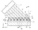
- Sectional drawing which shows typically the light-emitting device which concerns on a reference example.
- the top view which shows typically the light-emitting device which concerns on 1st Embodiment.
- Sectional drawing which shows typically the light-emitting device which concerns on the 1st modification of 1st Embodiment.
- Sectional drawing which shows typically the light-emitting device which concerns on the 2nd modification of 1st Embodiment.
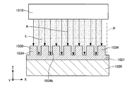
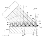
- FIG. 1 is a cross-sectional view schematically showing a light emitting device 100 according to the first embodiment.
- FIG. 2 is a plan view schematically showing the light emitting device 100 according to the first embodiment.
- 1 is a cross-sectional view taken along the line II of FIG. In FIGS. 1 and 2, the X axis, the Y axis, and the Z axis are illustrated as three axes orthogonal to each other.
- the light emitting device 100 includes a light source 10, a base 20, and a phosphor 30 as shown in FIGS. For convenience, the illustration of the light source 10 is omitted in FIG.
- the light source 10 emits light (excitation light) L that brings the phosphor 30 into an excited state.
- the light source 10 emits light L obliquely with respect to the first surface 21 of the base body 20.
- the optical axis A of the light L emitted from the light source 10 (hereinafter also simply referred to as “light L”) intersects the normal P of the first surface 21, for example.
- the normal line P is parallel to the Z axis.
- the light L enters the phosphor 30 from the direction intersecting the normal line P.
- the optical axis A is, for example, an axis parallel to the light beam having the highest intensity among the light L.
- the direction of the optical axis A (the extending direction of the optical axis A) intersects the thickness direction of the substrate 20.
- the angle ⁇ formed by the normal line P and the optical axis A is, for example, 5 ° to 45 °, and preferably 20 ° to 40 °.
- the light L emitted from the light source 10 is, for example, blue light.
- the wavelength of the light L is, for example, not less than 435 nm and not more than 480 nm.
- the light source 10 includes, for example, a light emitting element such as a laser or an LED (Light Emitting Diode).
- the light source 10 may be configured by arranging light emitting elements in an array.
- the base body 20 has, for example, a flat shape.
- the base 20 has a first surface 21.
- the first surface 21 is a flat surface.
- the material of the base 20 is, for example, Al, Cu, GaN, sapphire, or the like.
- the base body 20 may be configured by laminating a sapphire substrate and a GaN layer having the first surface 21.
- the phosphor 30 is provided in a film shape on the first surface 21 of the base body 20. In the illustrated example, the phosphor 30 is provided so as to cover the entire surface of the first surface 21.
- the phosphor 30 emits light by the light L emitted from the light source 10. Specifically, for example, the phosphor 30 absorbs the light L and emits light by fluorescence. The fluorescence occurs particularly on the surface of the phosphor 30. If the light L is incident on the phosphor 30, it may or may not be incident on the substrate 20.
- the phosphor refers to a substance that emits light by irradiated light, and is not limited to a substance that emits light by fluorescence, but includes, for example, a substance that emits light by phosphorescence.
- the light emitted from the phosphor 30 is, for example, yellow light.
- the wavelength of the light emitted from the phosphor 30 is, for example, not less than 580 nm and not more than 595 nm.
- Examples of the material of the phosphor 30 include sialon (a ceramic material made of silicon, aluminum, oxygen, and nitrogen), YAG (a crystal material with a garnet structure made of yttrium and aluminum), InGaN, and the like.
- the phosphor 30 has, for example, a flat plate portion 32 and a protruding portion 34.
- the flat plate portion 32 is provided on the first surface 21.
- the flat plate portion 32 has a flat plate shape.
- the thickness (size in the Z-axis direction) of the flat plate portion 32 is, for example, not less than 0.1 ⁇ m and not more than 10 ⁇ m.
- the protruding portion 34 protrudes from the flat plate portion 32 in the + Z-axis direction.
- the protrusion 34 has a columnar shape.
- the protrusion 34 has an upper surface (a surface facing the + Z axis direction in the illustrated example) 34a and a side surface (a surface orthogonal to the upper surface 34a in the illustrated example) 34b.
- the light L is incident on the upper surface 34a and the side surface 34b. Further, the light L is incident on the upper surface 32 a of the flat plate portion 32.
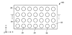
- a plurality of protrusions 34 are provided.
- the plurality of protrusions 34 are provided to be separated from each other.
- the plurality of protrusions 34 are arranged in a square lattice shape in plan view (as viewed from the Z-axis direction).
- the light L enters the phosphor 30 from the X-axis direction or the Y-axis direction in plan view.
- the width of the protrusion 34 (the size in the direction orthogonal to the Z-axis direction) is, for example, not less than 10 nm and not more than 5 ⁇ m.
- the height (size in the Z-axis direction) of the protrusion 34 is, for example, not less than 0.1 ⁇ m and not more than 10 ⁇ m.
- the interval between the adjacent protrusions 34 is, for example, 5 nm or more and 5 ⁇ m or less.
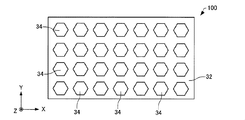
- the planar shape (shape seen from the Z-axis direction) of the protruding portion 34 is, for example, a circle.
- the planar shape of the projecting portion 34 (the shape of the projecting portion 34 in plan view as viewed from the normal P direction) may be an ellipse, a quadrangle, a hexagon (see FIG. 3), or the like. It may be a polygon.
- the width of the protruding portion 34 does not change in the Z-axis direction, but may change.
- the phosphor 30 has a second surface 31.
- the second surface 31 is a surface opposite to the base 20 side of the phosphor 30.
- the second surface 31 has an uneven shape.
- the uneven shape of the second surface 31 is formed by the flat plate portion 32 and the protruding portion 34.
- the uneven shape of the second surface 31 is a shape reflecting the shapes of the flat plate portion 32 and the protruding portion 34.
- the direction of the optical axis A of the light L intersects with the protruding direction (Z-axis direction in the illustrated example) of the convex portion 31a constituting the concave and convex shape of the second surface 31.
- the convex portion 31 a is constituted by a protruding portion 34.
- the protruding directions of the plurality of convex portions 31a are, for example, the same.
- the light source 10 irradiates the light L obliquely with respect to the uneven shape of the second surface 31.
- “irradiate light L obliquely with respect to the concavo-convex shape of the second surface 31” means the protruding direction of the convex portion 31 a constituting the concavo-convex shape of the second surface 31 and the light of the light L. This refers to irradiating light so that the direction of the axis A intersects.
- the “projection direction of the convex portion 31a” refers to the center point C1 of the bottom surface 134 of the projection 34 and the height of the projection 34 (maximum in the normal P direction as viewed in the normal P direction). It is the direction of the center line ⁇ that connects the center point C2 of the cross section 136 of the protrusion 34 in a plan view as viewed from the normal P direction at a position 1/2 of the dimension).
- the bottom surface of the protruding portion 34 is a surface that is in contact with the flat plate portion 32 of the protruding portion 34.
- the “center point C1 of the bottom surface 134” is the center of the smallest circle (minimum inclusion circle) that includes the shape of the bottom surface 134 inside.
- the “center point C2 of the cross section 136” is the center of the smallest circle including the shape of the cross section 136 inside.
- the cross section 136 of the protrusion 34 at a position that is 1/2 the height of the protrusion 34 means that the center line ⁇ of the protrusion 34 at a position that is 1/2 the height of the protrusion 34. It is a cross section orthogonal to.
- the light emitting device 100 has the following features, for example.
- the light emitting device 100 includes a phosphor 30 that is provided in a film shape on the first surface 21 of the base 20 and emits light by the light L emitted from the light source 10, and is opposite to the base 20 side of the phosphor 30.
- the second surface 31 has an uneven shape, and the light source 10 irradiates the light L obliquely with respect to the uneven shape of the second surface 31. Therefore, in the light emitting device 100, the side surface of the convex portion 31a (the side surface 34b of the protruding portion 34) can be irradiated with the light L. Therefore, in the light emitting device 100, the light emission rate can be improved.
- the light emitting device 100 even if the output of the light L is reduced, the output of the light emitted from the phosphor 30 can be maintained. Therefore, in the light emitting device 100, for example, when the light source 10 is configured by a plurality of light emitting elements, the number of light emitting elements can be reduced. As a result, in the light emitting device 100, cost reduction can be achieved. Further, in the light emitting device 100, since the output of the light L can be reduced, the life can be extended.
- irradiating the light L obliquely with respect to the concavo-convex shape means that the light is applied to the protrusion 34 so that the protrusion direction of the protrusion 34 intersects the direction of the optical axis A of the light L. It expresses that L is irradiated.
- the light emission rate can be improved as compared with the light emitting device as shown in FIG.
- the light L transmitted through the convex portion 31a can be incident on at least one of the convex portion 31a adjacent to the convex portion 31a and the flat plate portion 32. Therefore, in the light emitting device 100, the light emission rate can be improved.
- the plurality of protrusions 34 are provided apart from each other. Therefore, in the light emitting device 100, the total surface area of the phosphor 30 can be increased as compared with the case where the plurality of protrusions 34 are provided continuously. Therefore, in the light emitting device 100, heat dissipation can be improved.
- the direction of the optical axis A of the light L emitted from the light source 10 intersects the protruding direction of the convex portion 31 a constituting the concave and convex shape of the second surface 31. Therefore, in the light emitting device 100, the side surface of the convex portion 31a can be irradiated with the light L.
- the phosphor 30 includes a flat plate portion 32 that is provided on the first surface 21 and has a flat plate shape, and a protruding portion 34 that protrudes from the flat plate portion 32.
- the uneven shape is formed by the flat plate portion 32 and the protruding portion 34. Therefore, in the light emitting device 100, for example, the second surface 31 of the phosphor 30 can be formed into an uneven shape without processing (patterning) the base body 20 into an uneven shape.
- the plurality of protrusions 34 may be arranged in a triangular lattice shape in plan view.
- the light L enters the phosphor 30 from a direction inclined by 60 ° with respect to the X axis, or from the X axis direction.
- the light source 10 is not shown in FIG.
- the plurality of protrusions 34 may be provided in a stripe shape in plan view.
- the protruding direction of the protruding portion 34 coincides with the normal P direction, but the present invention is not limited to this, and the protruding direction may not coincide with the normal P direction. .
- the protruding direction does not coincide with the normal P direction, for example, the normal P and the optical axis A may be parallel.
- a phosphor 30 is formed on the first surface 21 of the base 20.
- a light emitting film (not shown) is formed by, for example, a CVD (Chemical Vapor Deposition) method, a sputtering method, or the like.
- the light emitting film is patterned by, for example, photolithography and etching. Etching is stopped before the substrate 20 is exposed. Thereby, the phosphor 30 having the flat plate portion 32 and the protruding portion 34 can be formed.
- the light source 10 is arranged at a position where the light L can be emitted obliquely with respect to the first surface 21.
- the light emitting device 100 can be manufactured through the above steps.
- FIG. 6 is a cross-sectional view schematically showing a light emitting device 110 according to a first modification of the first embodiment. 6 and FIGS. 7 and 8 shown below, the X axis, the Y axis, and the Z axis are illustrated as three axes orthogonal to each other.
- the uneven shape of the second surface 31 of the phosphor 30 is formed by the flat plate portion 32 and the protruding portion 34 of the phosphor 30.
- the uneven shape of the second surface 31 is formed by the flat plate portion 22 and the protruding portion 24 of the base body 20.
- the uneven shape of the second surface 31 is a shape reflecting the shapes of the flat plate portion 22 and the protruding portion 24.
- the first surface 21 of the base body 20 has an uneven shape.
- the base body 20 has a flat plate portion 22 and a protruding portion 24.
- the flat plate portion 22 has a flat plate shape.
- the protruding portion 24 protrudes from the flat plate portion 22 in the + Z-axis direction.
- the protrusion 24 has a columnar shape.
- the protrusion 24 has an upper surface (a surface facing the + Z axis direction in the illustrated example) 24a and a side surface (a surface orthogonal to the upper surface 24a in the illustrated example) 24b.
- the light L enters the phosphor 30 provided on the upper surface 24a and the phosphor 30 provided on the side surface 24b. Further, the light L is incident on the phosphor 30 provided on the upper surface 22 a of the flat plate portion 22.
- the optical axis A of the light L intersects the normal line R of the upper surface 24a. In the illustrated example, the normal line R is parallel to the Z axis.
- a plurality of protrusions 24 are provided.
- the plurality of protrusions 24 are provided to be separated from each other.
- the description of the protrusions 34 of the phosphor 30 described above can be applied to the shape and size of the protrusions 24 and the arrangement of the plurality of protrusions 24.
- the convex portion 31 a includes the protruding portion 24.
- the “projection direction of the convex portion 31a” refers to the center point C3 of the bottom surface 124 of the projection portion 24 and the height of the projection portion 24 (normal line R) in plan view as viewed from the normal P direction. This is the direction of the center line ⁇ connecting the center point C4 of the cross-section 126 of the protrusion 24 in plan view as viewed from the normal P direction at a position 1/2 of the maximum dimension in the direction).
- the bottom surface of the protrusion 24 is a surface that is in contact with the flat plate portion 22 of the protrusion 24.
- the phosphor 30 is provided so as to cover the flat plate portion 22 and the protruding portion 24.
- the thickness of the phosphor 30 is smaller than the height of the protrusion 24.
- the substrate 20 having the flat plate portion 22 and the protruding portion 24 is formed by patterning the substrate by, for example, photolithography and etching.
- the phosphor 30 is formed on the first surface 21 of the substrate 20 by, for example, a CVD method or a sputtering method.
- the light emitting device 110 can have the same effect as the light emitting device 100 described above.
- the base body 20 includes a flat plate portion 22 having a flat plate shape and a protruding portion 24 protruding from the flat plate portion 22, and the concave and convex shape of the second surface 31 has the flat plate portion 22 and a protruding shape.
- the portion 24 is formed. Therefore, in the light emitting device 110, it is possible to form an uneven shape on the second surface 31 of the phosphor 30 only by forming the phosphor 30 on the first surface 21 of the base body 20 without patterning the phosphor 30. it can.
- FIG. 7 is a cross-sectional view schematically showing a light emitting device 120 according to a second modification of the first embodiment.
- the uneven shape of the second surface 31 of the phosphor 30 is formed by the flat plate portion 32 and the protruding portion 34 of the phosphor 30.
- the uneven shape of the second surface 31 is formed by the flat plate portion 42 and the protruding portion 44 of the base layer 40.
- the uneven shape of the second surface 31 is a shape reflecting the shapes of the flat plate portion 42 and the protruding portion 44.
- the base layer 40 is provided on the first surface 21 of the base body 20.
- the base layer 40 is provided between the base body 20 and the phosphor 30.
- the material of the base layer 40 is different from the material of the base body 20.
- the material of the base layer 40 is, for example, a semiconductor material such as GaN or InGaN.
- the base layer 40 has a flat plate portion 42 and a protruding portion 44.
- the flat plate portion 42 is provided on the first surface 21.
- the flat plate part 42 has a flat plate shape.
- the protruding portion 44 protrudes from the flat plate portion 42 in the + Z-axis direction.
- the protrusion 44 has a columnar shape.
- the projecting portion 44 has an upper surface (a surface facing the + Z axis direction in the illustrated example) 44a and a side surface (a surface orthogonal to the upper surface 44a in the illustrated example) 44b.
- the light L is incident on the phosphor 30 provided on the upper surface 44a and the phosphor 30 provided on the side surface 44b. Further, the light L enters the phosphor 30 provided on the upper surface 42 a of the flat plate portion 42.
- a plurality of protrusions 44 are provided.
- the plurality of protrusions 44 are provided apart from each other.
- the description of the protrusions 34 of the phosphor 30 described above can be applied to the shape and size of the protrusions 44 and the arrangement of the plurality of protrusions 44.
- the convex portion 31 a includes the protruding portion 44.
- the “projection direction of the convex portion 31a” refers to the center point C5 of the bottom surface 144 of the projection 44 in plan view as viewed from the normal P direction and the height of the projection 44 (normal P). This is the direction of the center line ⁇ that connects the center point C6 of the cross section 146 of the protrusion 44 in plan view when viewed from the normal P direction at a position 1/2 of the maximum dimension in the direction).
- the bottom surface of the protruding portion 44 is a surface that is in contact with the flat plate portion 42 of the protruding portion 44.
- the phosphor 30 is provided so as to cover the flat plate portion 42 and the protruding portion 44.
- the phosphor 30 is provided on the first surface 21 of the base body 20 via the base layer 40.
- the thickness of the phosphor 30 is smaller than the height of the protrusion 44.
- a base film (not shown) is formed on the first surface 21 of the base 20 by, for example, MOCVD (Metal Organic Chemical Deposition) method or MBE (Molecular Beam Epitaxy) method, The light emitting film is patterned by photolithography and etching. Etching is stopped before the substrate 20 is exposed. Thereby, the base layer 40 having the flat plate portion 42 and the protruding portion 44 can be formed.
- the phosphor 30 is formed on the base layer 40 by, for example, a CVD method or a sputtering method.
- the light emitting device 120 can have the same effect as the light emitting device 100 described above.
- the light emitting device 120 includes a base layer 40 provided between the base body 20 and the phosphor 30, and the phosphor 30 is provided on the first surface 21 via the base layer 40. It has a flat plate portion 42 that is provided on one surface 21 and has a flat plate shape, and a protruding portion 44 that protrudes from the flat plate portion 42, and the uneven shape of the second surface 31 is the flat plate portion 42 and the protruding portion 44. Is formed by. Therefore, in the light emitting device 120, it is possible to form an uneven shape on the second surface 31 of the phosphor 30 without patterning the phosphor 30 or the base body 20.
- the light emitting device 120 does not have the flat plate portion 42, and the protruding portion 44 may be provided on the first surface 21.
- the phosphor 30 is provided so as to cover the protrusion 44 and the first surface 21.
- the bottom surface of the protruding portion 44 is a surface in contact with the base body 20 of the protruding portion 44.
- FIG. 9 is a cross-sectional view schematically showing the light emitting device 200 according to the second embodiment.
- an X axis, a Y axis, and a Z axis are illustrated as three axes orthogonal to each other.
- the light source 10 includes a light emitting element 12 that emits light and an optical element 14 that bends the optical axis A of the light from the light emitting element 12. Different from the light emitting device 100 described above. Further, the light source 10 of the light emitting device 200 includes a condensing optical system 16 and a lens 18.
- the light emitting element 12 is, for example, a laser or an LED.
- a plurality of light emitting elements 12 (three in the illustrated example) are provided.
- the light emitting element 12 emits light in the Z-axis direction.
- the condensing optical system 16 includes a lens 16a that is a plurality of convex lenses, and a lens 16b that is a convex lens through which light through the plurality of lenses 16a is incident in common.
- the condensing optical system 16 is disposed on the optical axis A of the light emitted from the light emitting element 12 and condenses the light emitted from the plurality of light emitting elements 12.
- the light emitted from the condensing optical system 16 enters the lens 18.
- the lens 18 collimates the light emitted from the light emitting element 12.
- the light emitted from the lens 18 enters the optical element 14.
- the optical element 14 bends the optical axis A of the light from the light emitting element 12 and reflects the light obliquely with respect to the uneven shape of the second surface 31 of the phosphor 30.
- the light source 10 can emit light obliquely with respect to the uneven shape of the second surface 31.
- the optical element 14 is, for example, a mirror.
- the light source 10 irradiates the light L obliquely with respect to the concavo-convex shape of the second surface 31.
- the light L from the light source 10 directly irradiates the concavo-convex shape of the second surface 31 obliquely.
- the optical element A bends the optical axis A of the light L (changes the direction of the optical axis A) so that the light L from the light source 10 is irradiated obliquely with respect to the concave-convex shape of the second surface 31. It is also an expression that includes
- the optical element 14 is not limited to a mirror, and may be, for example, a prism, a diffraction grating, or a half mirror. May be.
- the optical element 14 may be a computer-generated hologram (CGH).
- CGH computer-generated hologram
- the light emitting device 200 can have the same effects as the light emitting device 100 described above.
- the light source 10 includes a light emitting element 12 that emits light and an optical element 14 that bends the optical axis A of the light emitted from the light emitting element 12. Therefore, in the light emitting device 200, the light emitted from the light emitting element 12 can be incident on the phosphor 30 via the optical element 14. Therefore, in the light emitting device 200, the degree of freedom of arrangement of the light emitting elements 12 can be increased.
- the light emitting device 200 according to the second embodiment is the light emitting device according to the first embodiment described above, except that the light emitting element 12, the optical element 14, the condensing optical system 16, and the lens 18 are arranged at predetermined positions. This is basically the same as 100 manufacturing methods. Therefore, the detailed description is abbreviate
- FIG. 10 is a cross-sectional view schematically showing the light emitting device 210 according to the second embodiment.
- an X axis, a Y axis, and a Z axis are illustrated as three axes orthogonal to each other.
- the light emitting device 210 is different from the above-described light emitting device 200 in that it includes a drive unit 50 that rotates the base body 20 about an axis (virtual axis) Q parallel to the normal line P.
- the rotation axis Q is an axis that extends in the extending direction of the convex portion 31 a constituting the concave-convex shape of the second surface 31.
- the light emitting device 210 includes a support shaft portion 52.
- the drive unit 50 is, for example, a motor.
- the support shaft portion 52 connects the drive unit 50 and the base body 20.
- the support shaft 52 extends from the drive unit 50 to the base body 20 in the Z-axis direction.
- the support shaft portion 52 is provided on the rotation shaft Q.
- the driving unit 50 is driven, the support shaft unit 52 is rotated.
- the base 20 can rotate around the rotation axis Q.
- the rotation axis Q may pass through the center of the base body 20 in plan view.
- the light emitting device 210 can have the same effect as the light emitting device 200 described above.
- the light emitting device 210 includes a drive unit 50 that rotates the base body 20 with the axis Q extending in the extending direction of the convex portion 31a constituting the concave and convex shape of the second surface 31 as a rotation axis. Therefore, in the light emitting device 210, it is possible to prevent the same region of the phosphor 30 from being irradiated with the light emitted from the light source 10 and dissolving the region.
- the light source 10 may include the light emitting element 12, the optical element 14, the condensing optical system 16, and the lens 18.
- the light emitting devices 100, 110, and 120 described above may include the drive unit 50 and the support shaft unit 52.
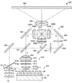
- FIG. 11 is a diagram schematically illustrating a projector 500 according to the third embodiment.
- the projector according to the present invention includes the light emitting device according to the present invention.
- a projector 500 including the light emitting device 200 as the light emitting device according to the present invention will be described.
- the projector 500 includes a housing (not shown), a light source module 510 provided in the housing, a color separation optical system 520, liquid crystal light valves (light modulation devices) 530R, 530G, and 530B, a color composition element 540, and Projection optical system 550.
- the projector 500 generally operates as follows.
- the light emitted from the light source module 510 is separated into a plurality of color lights by the color separation optical system 520.
- the plurality of color lights separated by the color separation optical system 520 are incident on the corresponding liquid crystal light valves 530R, 530G, and 530B and modulated.
- the plurality of color lights modulated by the liquid crystal light valves 530R, 530G, and 530B are incident on the color synthesis element 540 and synthesized.
- the light synthesized by the color synthesizing element 540 is enlarged and projected onto the screen 560 by the projection optical system 550, and a full-color projection image is displayed.
- the light source module 510 includes a light emitting device 200, a collimating optical system 511, lens arrays 512 and 513, a polarization conversion element 514, and a superimposing lens 515.
- the light emitting device 200 receives the light emitted from the light source 10 and emits the light emitted from the phosphor 30.
- the phosphor 30 receives, for example, blue light emitted from the light source 10 and emits yellow light.
- the optical element 14 is a half mirror. Part of the blue light emitted from the light source 10 passes through the optical element 14.
- the collimating optical system 511 includes a lens 511a that suppresses the spread of light emitted from the phosphor 30, and a lens 511b that collimates the light emitted from the lens 511a, and is emitted from the phosphor 30 as a whole. Parallelize the light.
- the lenses 511a and 511b are convex lenses.
- the lens arrays 512 and 513 make the luminance distribution of the light emitted from the collimating optical system 511 uniform.
- the lens array 512 has a plurality of lenses 512a.
- the lens array 513 has a plurality of lenses 513a.
- the lens 512a has a one-to-one correspondence with the lens 513a.
- Light emitted from the collimating optical system 511 is spatially divided and incident on a plurality of lenses 512a.
- the lens 512a forms an image of the incident light on the corresponding lens 513a. Thereby, a secondary light source image is formed on each of the plurality of lenses 513a.
- the outer shapes of the lenses 512a and 513a are substantially similar to the outer shapes of the image forming areas of the liquid crystal light valves 530R, 530G, and 530B.
- the polarization conversion element 514 aligns the polarization state of the light emitted from the lens arrays 512 and 513. For example, the polarization conversion element 514 emits incident light as P-polarized light.
- the haze superimposing lens 515 superimposes the light emitted from the polarization conversion element 514 in the illuminated area.
- the light emitted from the superimposing lens 515 is spatially divided and then superposed to make the luminance distribution uniform.
- the amber color separation optical system 520 includes dichroic mirrors 521, 522, mirrors 523, 524, 525, 526, relay lenses 527, 528, and field lenses 529R, 529G, 529B.
- the dichroic mirrors 521 and 522 are formed, for example, by laminating a dielectric multilayer film on the glass surface.
- the dichroic mirrors 521 and 522 have characteristics of selectively reflecting color light in a predetermined wavelength band and transmitting color light in other wavelength bands.
- the dichroic mirrors 521 and 522 reflect green light.
- the light emitted from the superimposing lens 515 is yellow light Y and enters the dichroic mirror 521.
- the red light R of the yellow light Y enters the mirror 523 through the dichroic mirror 521, is reflected by the mirror 523, and enters the field lens 529R.
- the red light R is collimated by the field lens 529R and then enters the liquid crystal light valve 530R.
- the green light G of the yellow light Y is reflected by the dichroic mirror 521 and then reflected by the dichroic mirror 522 and enters the field lens 529G.
- the green light G is collimated by the field lens 529G and then enters the liquid crystal light valve 530G.
- the blue light B transmitted through the optical element 14 is reflected by the mirror 524, then reflected by the mirror 525 through the dichroic mirrors 521 and 522 and the relay lens 527, and further reflected by the mirror 526 through the relay lens 528.
- the light enters the field lens 529B.
- the blue light B is collimated by the field lens 529B and then enters the liquid crystal light valve 530B.
- the liquid crystal light valves 530R, 530G, and 530B are configured by a light modulation device such as a transmissive liquid crystal light valve, for example.
- the liquid crystal light valves 530R, 530G, and 530B are electrically connected to a signal source (not shown) such as a PC that supplies an image signal including image information.
- the liquid crystal light valves 530R, 530G, and 530B modulate the incident light for each pixel based on the supplied image signal to form an image.
- the liquid crystal light valves 530R, 530G, and 530B form a red image, a green image, and a blue image, respectively.
- Light (formed image) modulated by the liquid crystal light valves 530R, 530G, and 530B is incident on the color composition element 540.
- the amber composition element 540 is configured by a dichroic prism or the like.
- the dichroic prism has a structure in which four triangular prisms are bonded to each other. The surface to be bonded in the triangular prism becomes the inner surface of the dichroic prism.
- a mirror surface that reflects red light and transmits green light and a mirror surface that reflects blue light and transmits green light are formed orthogonal to each other.
- the green light incident on the dichroic prism is emitted as it is through the mirror surface.
- the red light and blue light incident on the dichroic prism are selectively reflected or transmitted by the mirror surface and emitted in the same direction as the emission direction of the green light. In this way, the three color lights (images) are superimposed and synthesized, and the synthesized color lights are enlarged and projected onto the screen 560 by the projection optical system 550.
- the projector 500 includes a light emitting device 200 that can improve the light emission efficiency. Therefore, the projector 500 can have high luminance.
- the optical element 14 is a half mirror. Therefore, the projector 500 can emit red light, green light, and blue light without using a plurality of light source modules 510, and can be downsized.
- a transmissive liquid crystal light valve is used as the light modulator, but a light valve other than liquid crystal may be used, or a reflective light valve may be used.
- a light valve include a reflective liquid crystal light valve and a digital micromirror device (Digital Micromirror Device).
- the configuration of the projection optical system is appropriately changed depending on the type of light valve used.
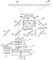
- FIG. 12 is a diagram schematically showing a projector 600 according to a first modification of the third embodiment.
- the projector 500 described above includes the light emitting device 200 as shown in FIG.
- the projector 600 includes a light emitting device 210 as shown in FIG.
- the projector according to the present invention is not limited to the light emitting devices 200 and 210, and can include the light emitting device according to the present invention.
- the projector 600 can have the same effect as the projector 500 described above.
- the projector 600 includes the light emitting device 210, it is possible to prevent the same region of the phosphor 30 from being irradiated with the light emitted from the light source 10 and dissolving the region.
- FIG. 13 is a diagram schematically illustrating a projector 700 according to a second modification of the third embodiment.
- the optical element 14 is a half mirror.
- the optical element 14 is a mirror and does not transmit the light emitted from the light emitting element 12.
- the projector 700 includes a light source module 710.
- the light source module 710 includes a light emitting element 12, a condensing optical system 16, lens arrays 512 and 513, a polarization conversion element 514, and a superimposing lens 515.
- the light source module 710 emits blue light B.
- the blue light B emitted from the light source module 710 passes through the field lens 529R and enters the liquid crystal light valve 530B.
- the light source module 510 includes a light emitting device 210.
- the color separation optical system 520 does not include the dichroic mirror 522, the mirrors 524, 525, and 526, and the relay lenses 527 and 528 but includes the mirror 722 that reflects the green light G.
- the projector 700 can have the same effect as the projector 500 described above.
- a part of the configuration may be omitted within a range having the characteristics and effects described in the present application, or each embodiment or modification may be combined.
- the present invention includes substantially the same configuration (for example, a configuration having the same function, method and result, or a configuration having the same purpose and effect) as the configuration described in the embodiment.
- the invention includes a configuration in which a non-essential part of the configuration described in the embodiment is replaced.
- the present invention includes a configuration that exhibits the same operational effects as the configuration described in the embodiment or a configuration that can achieve the same object.
- the invention includes a configuration in which a known technique is added to the configuration described in the embodiment.
- DESCRIPTION OF SYMBOLS 10 ... Light source, 12 ... Light emitting element, 14 ... Optical element, 16 ... Condensing optical system, 16a, 16b ... Lens, 18 ... Lens, 20 ... Base
- Relay lens 529R, 529G, 529B ... Field lens, 530R, 530G, 530B ... Liquid crystal light valve, 540 ... Color composition element, 550 ... Projection optical system, 560 ... Screen, 600, 700 ... Projector, 710 ... Light source module, 722 ... Mirror, 1010 ... Light source, 1020 ... Base, 1030 ... Phosphor, 1034 ... Projection, 1034b ... Side
Landscapes
- Physics & Mathematics (AREA)
- Engineering & Computer Science (AREA)
- Spectroscopy & Molecular Physics (AREA)
- Multimedia (AREA)
- General Engineering & Computer Science (AREA)
- General Physics & Mathematics (AREA)
- Optics & Photonics (AREA)
- Signal Processing (AREA)
- Projection Apparatus (AREA)
- Non-Portable Lighting Devices Or Systems Thereof (AREA)
- Optical Filters (AREA)
- Led Device Packages (AREA)
- Semiconductor Lasers (AREA)
Priority Applications (2)
| Application Number | Priority Date | Filing Date | Title |
|---|---|---|---|
| CN201880034906.1A CN110710067A (zh) | 2017-05-31 | 2018-05-22 | 发光装置和投影仪 |
| US16/618,082 US11061311B2 (en) | 2017-05-31 | 2018-05-22 | Light emitter and projector |
Applications Claiming Priority (2)
| Application Number | Priority Date | Filing Date | Title |
|---|---|---|---|
| JP2017-108389 | 2017-05-31 | ||
| JP2017108389A JP6988173B2 (ja) | 2017-05-31 | 2017-05-31 | 発光装置およびプロジェクター |
Publications (1)
| Publication Number | Publication Date |
|---|---|
| WO2018221317A1 true WO2018221317A1 (ja) | 2018-12-06 |
Family
ID=64454645
Family Applications (1)
| Application Number | Title | Priority Date | Filing Date |
|---|---|---|---|
| PCT/JP2018/019641 Ceased WO2018221317A1 (ja) | 2017-05-31 | 2018-05-22 | 発光装置およびプロジェクター |
Country Status (4)
| Country | Link |
|---|---|
| US (1) | US11061311B2 (https=) |
| JP (1) | JP6988173B2 (https=) |
| CN (1) | CN110710067A (https=) |
| WO (1) | WO2018221317A1 (https=) |
Families Citing this family (2)
| Publication number | Priority date | Publication date | Assignee | Title |
|---|---|---|---|---|
| TW202138899A (zh) * | 2020-04-14 | 2021-10-16 | 日商索尼股份有限公司 | 光學元件、照明裝置及投影型顯示裝置 |
| CN113671780A (zh) * | 2021-08-31 | 2021-11-19 | 青岛海信激光显示股份有限公司 | 发光单元、光源系统和激光投影设备 |
Citations (8)
| Publication number | Priority date | Publication date | Assignee | Title |
|---|---|---|---|---|
| JPH06176692A (ja) * | 1992-12-03 | 1994-06-24 | Nissha Printing Co Ltd | 蛍光膜形成方法および転写シート |
| JP2006179658A (ja) * | 2004-12-22 | 2006-07-06 | Mitsubishi Electric Corp | 発光装置 |
| JP2012104267A (ja) * | 2010-11-08 | 2012-05-31 | Stanley Electric Co Ltd | 光源装置および照明装置 |
| JP2012162600A (ja) * | 2011-02-03 | 2012-08-30 | Sharp Corp | 発光素子、発光装置、車両用前照灯、照明装置及び発光素子の製造方法 |
| JP2013203822A (ja) * | 2012-03-28 | 2013-10-07 | Nichia Corp | 色変換用無機成形体及びその製造方法、並びに発光装置 |
| WO2017026118A1 (ja) * | 2015-08-10 | 2017-02-16 | 富士フイルム株式会社 | 蛍光体含有フィルムおよびバックライトユニット |
| US20170235127A1 (en) * | 2016-02-12 | 2017-08-17 | Materion Corporation | Enhancement of output of optically pumped phosphor by use of surface nanostructures |
| WO2017195620A1 (ja) * | 2016-05-13 | 2017-11-16 | パナソニックIpマネジメント株式会社 | 光源装置及び照明装置 |
Family Cites Families (17)
| Publication number | Priority date | Publication date | Assignee | Title |
|---|---|---|---|---|
| JP2003020476A (ja) | 2001-07-10 | 2003-01-24 | Nippon Hoso Kyokai <Nhk> | 蛍光体薄膜、薄膜エレクトロルミネッセンス表示装置および電界放出型表示装置ならびに蛍光体薄膜形成方法 |
| JP2004302282A (ja) * | 2003-03-31 | 2004-10-28 | Japan Wavelock Co Ltd | 映写スクリーン |
| JP2006104411A (ja) | 2004-10-08 | 2006-04-20 | Sharp Corp | 蛍光体、その製造方法およびこれを用いた発光装置 |
| CN100464232C (zh) * | 2005-12-21 | 2009-02-25 | 中华映管股份有限公司 | 平面灯源 |
| JP5253740B2 (ja) | 2007-01-09 | 2013-07-31 | 学校法人上智学院 | Iii族窒化物半導体微細柱状結晶の製造方法およびiii族窒化物構造体 |
| JP5043472B2 (ja) | 2007-02-28 | 2012-10-10 | 学校法人上智学院 | Iii族窒化物半導体微細柱状結晶の製造方法およびiii族窒化物構造体 |
| EP2272102B1 (en) * | 2008-03-26 | 2016-06-22 | Panasonic Intellectual Property Management Co., Ltd. | Semiconductor light-emitting apparatus |
| JP5145120B2 (ja) | 2008-05-26 | 2013-02-13 | パナソニック株式会社 | 化合物半導体発光素子およびそれを用いる照明装置ならびに化合物半導体発光素子の製造方法 |
| JP5008631B2 (ja) | 2008-10-14 | 2012-08-22 | シャープ株式会社 | 蛍光体、その製造方法およびこれを用いた発光装置 |
| JP4742349B2 (ja) | 2009-06-30 | 2011-08-10 | カシオ計算機株式会社 | 光源装置及びプロジェクタ |
| JP5413613B2 (ja) | 2011-02-04 | 2014-02-12 | カシオ計算機株式会社 | 光源装置、その制御方法及びプロジェクタ |
| JP2012243624A (ja) * | 2011-05-20 | 2012-12-10 | Stanley Electric Co Ltd | 光源装置および照明装置 |
| WO2013103039A1 (ja) | 2012-01-07 | 2013-07-11 | 日本電気株式会社 | 光学素子、光学装置、画像表示装置および励起光の吸収率向上方法 |
| CN103367611B (zh) * | 2012-03-28 | 2017-08-08 | 日亚化学工业株式会社 | 波长变换用无机成型体及其制造方法以及发光装置 |
| JP6062249B2 (ja) * | 2013-01-09 | 2017-01-18 | 日立マクセル株式会社 | 車両用灯具 |
| JP6697225B2 (ja) * | 2015-05-25 | 2020-05-20 | スタンレー電気株式会社 | 照明装置 |
| US10174925B2 (en) * | 2015-12-25 | 2019-01-08 | Nichia Corporation | Wavelength conversion member and light source device having wavelength conversion member |
-
2017
- 2017-05-31 JP JP2017108389A patent/JP6988173B2/ja active Active
-
2018
- 2018-05-22 CN CN201880034906.1A patent/CN110710067A/zh active Pending
- 2018-05-22 US US16/618,082 patent/US11061311B2/en active Active
- 2018-05-22 WO PCT/JP2018/019641 patent/WO2018221317A1/ja not_active Ceased
Patent Citations (8)
| Publication number | Priority date | Publication date | Assignee | Title |
|---|---|---|---|---|
| JPH06176692A (ja) * | 1992-12-03 | 1994-06-24 | Nissha Printing Co Ltd | 蛍光膜形成方法および転写シート |
| JP2006179658A (ja) * | 2004-12-22 | 2006-07-06 | Mitsubishi Electric Corp | 発光装置 |
| JP2012104267A (ja) * | 2010-11-08 | 2012-05-31 | Stanley Electric Co Ltd | 光源装置および照明装置 |
| JP2012162600A (ja) * | 2011-02-03 | 2012-08-30 | Sharp Corp | 発光素子、発光装置、車両用前照灯、照明装置及び発光素子の製造方法 |
| JP2013203822A (ja) * | 2012-03-28 | 2013-10-07 | Nichia Corp | 色変換用無機成形体及びその製造方法、並びに発光装置 |
| WO2017026118A1 (ja) * | 2015-08-10 | 2017-02-16 | 富士フイルム株式会社 | 蛍光体含有フィルムおよびバックライトユニット |
| US20170235127A1 (en) * | 2016-02-12 | 2017-08-17 | Materion Corporation | Enhancement of output of optically pumped phosphor by use of surface nanostructures |
| WO2017195620A1 (ja) * | 2016-05-13 | 2017-11-16 | パナソニックIpマネジメント株式会社 | 光源装置及び照明装置 |
Also Published As
| Publication number | Publication date |
|---|---|
| US20200142289A1 (en) | 2020-05-07 |
| CN110710067A (zh) | 2020-01-17 |
| US11061311B2 (en) | 2021-07-13 |
| JP6988173B2 (ja) | 2022-01-05 |
| JP2018206863A (ja) | 2018-12-27 |
Similar Documents
| Publication | Publication Date | Title |
|---|---|---|
| EP3722874B1 (en) | Light source device, image projection apparatus, light source optical system | |
| JP5874058B2 (ja) | 光源装置および投写型表示装置 | |
| CN110737163B (zh) | 光源装置和投影仪 | |
| JP5966843B2 (ja) | 光源装置及び画像表示装置 | |
| CN104345531B (zh) | 光源装置及投影机 | |
| JP6136744B2 (ja) | 光源装置、及び画像表示装置 | |
| JP5716401B2 (ja) | 光源装置及びプロジェクター | |
| US20180217486A1 (en) | Light source device and projection display apparatus | |
| US10914453B2 (en) | Wavelength conversion device, illumination device, and projector | |
| WO2020137749A1 (ja) | 光源装置および投写型映像表示装置 | |
| WO2012137305A1 (ja) | 光源装置および投写型表示装置 | |
| JP2017083636A (ja) | 照明装置及びプロジェクター | |
| US20210191243A1 (en) | Light source apparatus and projection-type image display apparatus | |
| JP6354288B2 (ja) | 光源装置及びプロジェクター | |
| JP2005292561A (ja) | 光源装置および投写型表示装置 | |
| CN112987470B (zh) | 光源装置和投影仪 | |
| JP6988173B2 (ja) | 発光装置およびプロジェクター | |
| JP6911541B2 (ja) | 発光装置およびプロジェクター | |
| US12066752B2 (en) | Light-source device, image projection apparatus, and light-source optical system | |
| JP6206551B2 (ja) | 光源装置及び画像表示装置 | |
| JP2016162574A (ja) | 光源装置およびプロジェクター | |
| JP6217210B2 (ja) | 光源装置、およびプロジェクター | |
| CN114384747A (zh) | 光源装置、投影仪以及显示装置 | |
| JP2016142900A (ja) | 照明装置およびプロジェクター | |
| JP2015111308A (ja) | 光源装置及びプロジェクター |
Legal Events
| Date | Code | Title | Description |
|---|---|---|---|
| 121 | Ep: the epo has been informed by wipo that ep was designated in this application |
Ref document number: 18810626 Country of ref document: EP Kind code of ref document: A1 |
|
| NENP | Non-entry into the national phase |
Ref country code: DE |
|
| 122 | Ep: pct application non-entry in european phase |
Ref document number: 18810626 Country of ref document: EP Kind code of ref document: A1 |