WO2018216627A1 - 電子機器 - Google Patents
電子機器 Download PDFInfo
- Publication number
- WO2018216627A1 WO2018216627A1 PCT/JP2018/019358 JP2018019358W WO2018216627A1 WO 2018216627 A1 WO2018216627 A1 WO 2018216627A1 JP 2018019358 W JP2018019358 W JP 2018019358W WO 2018216627 A1 WO2018216627 A1 WO 2018216627A1
- Authority
- WO
- WIPO (PCT)
- Prior art keywords
- circuit board
- heat
- heat conduction
- hole
- conduction path
- Prior art date
- Legal status (The legal status is an assumption and is not a legal conclusion. Google has not performed a legal analysis and makes no representation as to the accuracy of the status listed.)
- Ceased
Links
Images



Classifications
-
- H—ELECTRICITY
- H10—SEMICONDUCTOR DEVICES; ELECTRIC SOLID-STATE DEVICES NOT OTHERWISE PROVIDED FOR
- H10W—GENERIC PACKAGES, INTERCONNECTIONS, CONNECTORS OR OTHER CONSTRUCTIONAL DETAILS OF DEVICES COVERED BY CLASS H10
- H10W40/00—Arrangements for thermal protection or thermal control
- H10W40/20—Arrangements for cooling
- H10W40/22—Arrangements for cooling characterised by their shape, e.g. having conical or cylindrical projections
- H10W40/226—Arrangements for cooling characterised by their shape, e.g. having conical or cylindrical projections characterised by projecting parts, e.g. fins to increase surface area
- H10W40/228—Arrangements for cooling characterised by their shape, e.g. having conical or cylindrical projections characterised by projecting parts, e.g. fins to increase surface area the projecting parts being wire-shaped or pin-shaped
-
- H—ELECTRICITY
- H05—ELECTRIC TECHNIQUES NOT OTHERWISE PROVIDED FOR
- H05K—PRINTED CIRCUITS; CASINGS OR CONSTRUCTIONAL DETAILS OF ELECTRIC APPARATUS; MANUFACTURE OF ASSEMBLAGES OF ELECTRICAL COMPONENTS
- H05K1/00—Printed circuits
- H05K1/02—Details
- H05K1/0201—Thermal arrangements, e.g. for cooling, heating or preventing overheating
- H05K1/0203—Cooling of mounted components
- H05K1/0204—Cooling of mounted components using means for thermal conduction connection in the thickness direction of the substrate
- H05K1/0206—Cooling of mounted components using means for thermal conduction connection in the thickness direction of the substrate by printed thermal vias
-
- H—ELECTRICITY
- H05—ELECTRIC TECHNIQUES NOT OTHERWISE PROVIDED FOR
- H05K—PRINTED CIRCUITS; CASINGS OR CONSTRUCTIONAL DETAILS OF ELECTRIC APPARATUS; MANUFACTURE OF ASSEMBLAGES OF ELECTRICAL COMPONENTS
- H05K3/00—Apparatus or processes for manufacturing printed circuits
- H05K3/30—Assembling printed circuits with electric components, e.g. with resistors
- H05K3/32—Assembling printed circuits with electric components, e.g. with resistors electrically connecting electric components or wires to printed circuits
- H05K3/34—Assembling printed circuits with electric components, e.g. with resistors electrically connecting electric components or wires to printed circuits by soldering
- H05K3/341—Surface mounted components
- H05K3/3431—Leadless components
- H05K3/3436—Leadless components having an array of bottom contacts, e.g. pad grid array or ball grid array components
-
- H—ELECTRICITY
- H05—ELECTRIC TECHNIQUES NOT OTHERWISE PROVIDED FOR
- H05K—PRINTED CIRCUITS; CASINGS OR CONSTRUCTIONAL DETAILS OF ELECTRIC APPARATUS; MANUFACTURE OF ASSEMBLAGES OF ELECTRICAL COMPONENTS
- H05K7/00—Constructional details common to different types of electric apparatus
- H05K7/20—Modifications to facilitate cooling, ventilating, or heating
- H05K7/2039—Modifications to facilitate cooling, ventilating, or heating characterised by the heat transfer by conduction from the heat generating element to a dissipating body
- H05K7/205—Heat-dissipating body thermally connected to heat generating element via thermal paths through printed circuit board [PCB]
-
- H—ELECTRICITY
- H05—ELECTRIC TECHNIQUES NOT OTHERWISE PROVIDED FOR
- H05K—PRINTED CIRCUITS; CASINGS OR CONSTRUCTIONAL DETAILS OF ELECTRIC APPARATUS; MANUFACTURE OF ASSEMBLAGES OF ELECTRICAL COMPONENTS
- H05K2201/00—Indexing scheme relating to printed circuits covered by H05K1/00
- H05K2201/06—Thermal details
- H05K2201/066—Heatsink mounted on the surface of the printed circuit board [PCB]
-
- H—ELECTRICITY
- H05—ELECTRIC TECHNIQUES NOT OTHERWISE PROVIDED FOR
- H05K—PRINTED CIRCUITS; CASINGS OR CONSTRUCTIONAL DETAILS OF ELECTRIC APPARATUS; MANUFACTURE OF ASSEMBLAGES OF ELECTRICAL COMPONENTS
- H05K2201/00—Indexing scheme relating to printed circuits covered by H05K1/00
- H05K2201/10—Details of components or other objects attached to or integrated in a printed circuit board
- H05K2201/10613—Details of electrical connections of non-printed components, e.g. special leads
- H05K2201/10621—Components characterised by their electrical contacts
- H05K2201/10734—Ball grid array [BGA]; Bump grid array
-
- H—ELECTRICITY
- H10—SEMICONDUCTOR DEVICES; ELECTRIC SOLID-STATE DEVICES NOT OTHERWISE PROVIDED FOR
- H10W—GENERIC PACKAGES, INTERCONNECTIONS, CONNECTORS OR OTHER CONSTRUCTIONAL DETAILS OF DEVICES COVERED BY CLASS H10
- H10W40/00—Arrangements for thermal protection or thermal control
- H10W40/70—Fillings or auxiliary members in containers or in encapsulations for thermal protection or control
- H10W40/73—Fillings or auxiliary members in containers or in encapsulations for thermal protection or control for cooling by change of state
-
- H—ELECTRICITY
- H10—SEMICONDUCTOR DEVICES; ELECTRIC SOLID-STATE DEVICES NOT OTHERWISE PROVIDED FOR
- H10W—GENERIC PACKAGES, INTERCONNECTIONS, CONNECTORS OR OTHER CONSTRUCTIONAL DETAILS OF DEVICES COVERED BY CLASS H10
- H10W70/00—Package substrates; Interposers; Redistribution layers [RDL]
- H10W70/60—Insulating or insulated package substrates; Interposers; Redistribution layers
- H10W70/62—Insulating or insulated package substrates; Interposers; Redistribution layers characterised by their interconnections
- H10W70/63—Vias, e.g. via plugs
- H10W70/635—Through-vias
-
- Y—GENERAL TAGGING OF NEW TECHNOLOGICAL DEVELOPMENTS; GENERAL TAGGING OF CROSS-SECTIONAL TECHNOLOGIES SPANNING OVER SEVERAL SECTIONS OF THE IPC; TECHNICAL SUBJECTS COVERED BY FORMER USPC CROSS-REFERENCE ART COLLECTIONS [XRACs] AND DIGESTS
- Y02—TECHNOLOGIES OR APPLICATIONS FOR MITIGATION OR ADAPTATION AGAINST CLIMATE CHANGE
- Y02P—CLIMATE CHANGE MITIGATION TECHNOLOGIES IN THE PRODUCTION OR PROCESSING OF GOODS
- Y02P70/00—Climate change mitigation technologies in the production process for final industrial or consumer products
- Y02P70/50—Manufacturing or production processes characterised by the final manufactured product
Definitions
- the present invention relates to a cooling structure for a heat generating component possessed by an electronic device.
- Some electronic devices have a heat sink such as a heat sink or heat pipe connected to an integrated circuit device such as a CPU or GPU.
- an integrated circuit device is arranged on the upper side of a circuit board, and a heat dissipation device is arranged on the upper side of the integrated circuit device (for example, JP 2013-222275 A).
- the heat dissipation device may restrict the layout of other components, or the cooling structure may be enlarged to obtain sufficient cooling performance.
- An electronic device proposed in the present disclosure is formed in a first surface on which an electronic component is disposed, a second surface opposite to the first surface, and a region in which the electronic component is disposed.
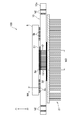
- FIG. 1 It is a schematic sectional drawing which shows an example of the electronic device proposed by this indication. It is an expanded sectional view of the circuit board which the electronic device of FIG. 1 has. It is a top view which shows the area
- the electronic device 1 has a circuit board 10.
- the circuit board 10 has a base material 10a formed of an insulating material such as paper phenol or glass epoxy resin.
- a circuit pattern 15 (see FIG. 2A) is formed on the substrate 10a.
- the circuit board 10 is a multilayer board having a plurality of layers, and a circuit pattern 15 is formed on each layer.
- the circuit board 10 may not be a multilayer board.
- the circuit board 10 may be a double-sided board in which the circuit pattern 15 is formed only on the upper surface and the lower surface, or a single-sided surface in which the circuit pattern 15 is formed only on the upper surface (the surface on which components such as integrated circuit devices are mounted). It may be a substrate.
- the circuit board 10 has holes h ⁇ b> 2 that connect the plurality of circuit patterns 15 to each other (hereinafter, the holes h ⁇ b> 2 are “connection holes”).
- a conductor 13 is formed inside the connection hole h ⁇ b> 2, and the plurality of circuit patterns 15 are electrically connected to each other through the conductor 13.
- metal plating is applied to the inside of the connection hole h2.
- the conductor 13 has a cylindrical shape, but unlike that, it may be formed so as to fill the connection hole h ⁇ b> 2.
- the connection hole h ⁇ b> 2 is a through hole that penetrates the circuit board 10, for example. Unlike this, the connection hole h ⁇ b> 2 may be a recess that does not penetrate the circuit board 10.
- the circuit board 10 further has a through hole h1 for forming a heat conduction path 11 to be described later.
- the electronic component is, for example, a heat generating component that generates heat during operation.
- the integrated circuit device 5 which is a heat generating component, is disposed on the circuit board 10.
- the integrated circuit device 5 is, for example, a microprocessor, a memory, an analog signal processing circuit, or the like, but is not limited thereto.
- the integrated circuit device 5 may be a SIP (system in package) in which a plurality of IC chips (silicon dies) are sealed in one package.
- the integrated circuit device 5 may be a Sip in which a plurality of IC chips are arranged horizontally, or a Sip in which a plurality of IC chips are arranged in the vertical direction.
- the integrated circuit device 5 includes two IC chips 5c and 5d that are stacked in the vertical direction.
- electronic components that are susceptible to temperature may be disposed on the circuit board 10. Examples of such electronic components may be sensors, LEDs (Light Emitting Diode), inverters, motors, and the like.
- the integrated circuit device 5 is a surface-mount type, and has a plurality of terminals connected to electrode pads 16 (see FIG. 2B) formed on the surface of the circuit board 10.
- the integrated circuit device 5 is a BGA (Ball Grid Array) type, and has a plurality of solder balls 5b (see FIG. 1) on the lower surface thereof. The solder balls 5b are connected to the electrode pads 6, respectively.
- the integrated circuit device 5 may not be a BGA type.
- the integrated circuit device 5 may have a plurality of lead terminals connected to the circuit board 10 on the outer peripheral edge of the integrated circuit device 5 instead of the solder balls.
- the integrated circuit device 5 may be an insertion mounting type having terminals that are inserted into holes formed in the circuit board 10 and soldered.
- a heat dissipating device is disposed on the lower surface (second surface) of the circuit board 10.
- a heat sink 21 is disposed on the lower surface of the circuit board 10.
- the heat sink 21 is located on the opposite side of the integrated circuit device 5 with the circuit board 10 interposed therebetween. That is, the heat sink 21 is disposed so as to overlap the integrated circuit device 5 in a plan view of the circuit board 10.
- the circuit board 10 has a through hole h1 (see FIG. 2A) penetrating the circuit board 10 in a region A where the integrated circuit device 5 is disposed.
- the area A is an area having a size corresponding to the external dimension of the integrated circuit device 5. That is, the area A means an area immediately below the integrated circuit device 5.
- the region A is a region that overlaps the integrated circuit device 5 in the plane of the circuit board 10.
- the through hole h ⁇ b> 1 continues from the upper surface to the lower surface of the circuit board 10.
- a heat conduction path 11 is provided in the through hole h1.
- a plurality of through holes h ⁇ b> 1 are formed in the area A in the circuit board 10, and the heat conduction path 11 is provided in each through hole h ⁇ b> 1.
- the heat conduction path 11 connects the integrated circuit device 5 and the heat sink 21, and the heat of the integrated circuit device 5 is transmitted to the heat sink 21 via the heat conduction path 11.
- the heat conduction path 11 is formed of a material having higher thermal conductivity than the base material 10 a of the circuit board 10.
- a space for the heat dissipation device is not required on the upper side of the integrated circuit device 5, so that another component 9 (for example, an antenna or the like) of the electronic device 1 is provided.
- another component 9 for example, an antenna or the like
- Transmission / reception module, sensor, external storage device, etc. can be arranged on the upper side of the integrated circuit device 5, and the degree of freedom in the layout of the components 9 can be increased.
- the component 9 is disposed on the opposite side of the heat sink 21 with the circuit board 10 and the integrated circuit device 5 interposed therebetween. That is, the component 9 is arranged at a position close to the upper side of the integrated circuit device 5.
- the distance L1 between the component 9 and the integrated circuit device 5 is smaller than the height H1 of the heat sink 21.
- another heat dissipation device may be disposed on the upper surface of the integrated circuit device 5. As a result, two heat dissipating devices are provided in the integrated circuit device 5, so that the cooling performance can be improved.
- the heat sink 21 is attached to the circuit board 10.
- the heat sink 21 is fixed to the circuit board 10 with a fixing tool such as a screw or a bolt, for example.
- the heat sink 21 may be soldered to the circuit board 10.
- a heat pipe may be disposed on the lower surface of the circuit board 10 as a heat dissipation device instead of the heat sink 21 or together with the heat sink 21.
- the heat conduction path 11 may connect the heat pipe and the integrated circuit device 5.
- the circuit board 10 has an electric circuit.
- the electric circuit is constituted by the circuit pattern 15 and the conductor 13 of the connection hole h2.
- the heat conduction path 11 is formed of the same material as the conductor 13, for example.
- the heat conduction path 11 in the manufacture of the circuit board 10, can be formed in the same process (plating process) as the conductor 13.
- the heat conduction path 11 may be formed of the same material as that of the circuit pattern 15.
- the heat conduction path 11 can be formed in the same process as the circuit pattern 15 in the manufacture of the circuit board 10.
- the conductor 13 and the circuit pattern 15 may be formed of the same material.
- the material of the circuit pattern 15, the conductor 13, and the heat conduction path 11 is, for example, copper.
- the heat conduction path 11 may be formed of a material different from the material of the electric circuit.
- the heat conduction path 11 may be formed of a material having a higher electric resistance than the material of the electric circuit. By doing so, it is possible to prevent the heat conduction path 11 and the heat sink 21 connected thereto from causing electromagnetic radiation noise (Electromagnetic Magnetic Interference, EMI).
- the circuit pattern 15 is formed of a conductive material (for example, copper), and the heat conduction path 11 is formed of, for example, a metal having higher electric resistance than copper.
- the heat conduction path 11 may be formed of an insulating material.
- the heat conduction path 11 may be formed of heat conduction grease (also referred to as “heat radiation grease”).
- the thermal conductive grease is a grease such as silicone mixed with a filler having high thermal conductivity (for example, particles of copper, silver, aluminum, or the like).
- the heat conduction grease is filled in the through hole h ⁇ b> 1 to form the heat conduction path 11.
- FIG. 2A in the example of the electronic device 1, the material of the heat conduction path 11 fills the through hole h1, and the heat conduction path 11 is columnar. By doing so, the heat of the integrated circuit device 5 can be efficiently transferred to the heat sink 21.
- the structure of the heat conduction path 11 is not limited to the example of FIG. 2A.
- FIG. 3 is a diagram showing another example of the heat conduction path 11 (the same reference numerals are given to the same portions as FIG. 2A in FIG. 3). As shown in FIG. 3, the heat conduction path 11 may have a cylindrical shape formed along the inner surface of the through hole h1.
- the 2A and 3 can be formed by, for example, a plating process performed in the manufacture of the circuit board 10.
- the heat conduction path 11 can be formed, for example, in a plating process for forming the conductor 13 of the connection hole h2.
- the method for forming the heat conduction path 11 is not limited to plating.
- the heat conduction path 11 may be a pin formed separately from the manufacture of the circuit board 10.
- the heat conduction grease 11 may be formed by inserting the heat conduction grease into the through hole h1.
- the heat conduction path 11 may be formed integrally with the heat sink 21. That is, a part of the heat sink 21 may be inserted into the through hole h 1, and this part may function as the heat conduction path 11.
- the through hole h1 is, for example, circular in the plan view of the circuit board 10.
- the through hole h1 can be formed relatively easily in the manufacture of the circuit board 10 as compared with the case where the through hole h1 is a square.
- the shape of the through hole h1 is not limited to a circle.
- the through hole h ⁇ b> 1 may be a long hole in a plan view of the circuit board 10.
- the circuit board 10 is formed with the connection holes h2 for connecting the plurality of circuit patterns 15.
- the width W1 (diameter) of the through hole h1 may be larger than the width (diameter) W2 of the connection hole h2.
- the size of the through hole h1 is not limited to the example of FIG. 2A.
- the width W1 (diameter) of the through hole h1 may be substantially the same as the width (diameter) W2 of the connection hole h2.
- the connection hole h ⁇ b> 2 shown in FIG. 3 does not penetrate the circuit board 10.
- the connection hole h ⁇ b> 2 connects two circuit patterns 15 formed inside the circuit board 10.
- the circuit board 10 has a plurality of through holes h1.
- the plurality of through holes h1 are arranged in a grid. That is, the plurality of through holes h1 are arranged at equal intervals in the vertical direction and the horizontal direction.
- an electric wire 15c that constitutes a part of the circuit pattern 15 may be formed between two adjacent through holes h1.
- the through holes h1 may be laid out so as to avoid the electric wires of the circuit pattern 15.
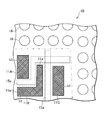
- FIG. 4 is a plan view showing a modification of the heat conduction path 11.
- the circuit board 10 has a plurality of heat conduction paths 11A, 11B, and 11C.
- An electric wire 15a constituting a part of the circuit pattern 15 is formed between two adjacent heat conduction paths 11A, 11B, and 11C.
- the heat conduction paths 11A, 11B, and 11C have different shapes and / or sizes in the plan view of the circuit board 10. Specifically, the heat conduction paths 11A and 11C are rectangular, whereas the heat conduction path 11B is L-shaped.
- the heat conduction path 11B is bent in accordance with the electric wire 15a.
- each heat conduction path 11A, 11B, 11C may be changed as appropriate in accordance with the shape of the circuit pattern 15. Moreover, the end part 11a (end part of the through-hole h1) of each heat conduction path 11A, 11B, 11C may be formed in circular arc shape. In this way, for example, it is easy to form the through hole h1 in which the heat conduction paths 11A, 11B, and 11C are formed.
- the integrated circuit device 5 has a heat conductive pad 5a on its lower surface.
- the solder ball 5b is formed outside the heat conductive pad 5a, but the position of the heat conductive pad 5a is not limited to this.
- the heat conductive pad 5a has a size larger than that of a terminal used for signal transmission / reception such as a solder ball 5b in the bottom view of the integrated circuit device 5.
- the heat conduction path 11 is connected to the heat conduction pad 5 a of the integrated circuit device 5.
- the plurality of heat conduction paths 11 are located in the region B (see FIG. 2B) of the heat conduction pad 5a and are connected to the heat conduction pad 5a.
- the heat conductive pad 5a is made of, for example, metal.
- the heat conductive pad 5 a may be used for electrical connection with the circuit board 10.
- the heat conductive pad 5a may be used as a ground line. That is, when the heat conduction path 11 is a conductor, the heat conduction path 11 is connected to a ground line formed on the circuit board 10, and the heat conduction path 11 and the heat conduction pad 5a are electrically and thermally connected to each other. May be connected.
- the heat conductive pad 5 a may not be used for electrical connection with the circuit board 10. That is, the heat conduction path 11 and the heat conduction pad 5a may be electrically independent from the circuit of the circuit board 10.
- connection member 31 that thermally connects these may be disposed between the heat conduction pad 5 a and the heat conduction path 11.
- the connection member 31 is, for example, solder. That is, when both the heat conductive pad 5a and the heat conductive path 11 are formed of metal, they are electrically and thermally connected to each other by, for example, solder.
- the connecting member 31 is not limited to solder.
- the connection member 31 may be heat conductive grease (also referred to as “heat radiation grease”) or a heat conductive sheet.
- the connecting member 31 is not necessarily limited to the heat conductive grease or the heat conductive sheet as long as it can be deformed so as to absorb the tolerance between the heat conductive path 11 and the heat conductive pad 5a.
- connection member 32 that thermally connects them may be disposed between the heat sink 21 and the heat conduction path 11.
- the connection member 32 is a heat conductive sheet, for example. This heat conductive sheet has elasticity in the thickness direction of the circuit board 10. By doing so, the connection stability between the heat sink 21 and the heat conduction path 11 can be secured, and when the heat sink 21 is pressed against the circuit board 10, it is possible to suppress the force from reaching the integrated circuit device 5. .
- the heat conductive sheet one containing silicone or one containing acrylic resin can be used.
- the connection member 32 may be the above-described heat conductive grease. Even in this case, the connection stability between the heat sink 21 and the heat conduction path 11 can be secured.
- FIG. 5 is a view showing a modification of the circuit board 10 (in this figure, the same reference numerals are given to the same portions as FIG. 2A).
- the circuit board 10 has a metal layer 18 on its lower surface (the surface facing the heat sink 21).
- the metal layer 18 is formed over the entire region where the plurality of through holes h ⁇ b> 1 are formed, and connects the plurality of heat conduction paths 11.
- the heat sink 21 is connected to the metal layer 18.
- the heat sink 21 may be in direct contact with the metal layer 18, and the connection member 32 such as the above-described heat conductive sheet or heat conductive grease is disposed between the heat sink 21 and the metal layer 18.
- the metal layer 18 is formed of the same material as the circuit pattern 15.
- the metal layer 18 and the circuit pattern 15 (specifically, the circuit pattern 15 formed on the lower surface of the circuit board 10) can be formed in the same process in the manufacture of the circuit board 10.
- a metal layer 17 that connects the plurality of heat conduction paths 11 is also formed on the upper surface of the circuit board 10.
- the metal layer 17 is formed, for example, over the entire region where the plurality of through holes h ⁇ b> 1 are formed, and connects the plurality of heat conduction paths 11.
- the heat conductive pad 5 a of the integrated circuit device 5 is connected to the metal layer 17.
- the heat conductive pad 5 a may be soldered to the metal layer 17.
- the connection member 31 such as the above-described heat conductive sheet or heat conductive grease may be disposed between the heat conductive pad 5 a and the metal layer 17.
- the metal layer 17 is formed of the same material as the circuit pattern 15.
- the metal layer 17 and the circuit pattern 15 (specifically, the circuit pattern 15 formed on the upper surface of the circuit board 10) can be formed in the same process in the manufacture of the circuit board 10.
- FIG. 6 is a cross-sectional view showing a modification of the heat conduction path 11.
- the circuit board 10 has one through hole h3.
- the through hole h3 has a width W3 larger than the width W2 of the connection hole h2 described above. More specifically, the width W3 is even larger than the interval W4 between the two solder balls 5b.
- the width W3 of the integrated circuit device 5 is larger than half of the size of the heat conductive pad 5a.
- the integrated circuit device 5 may substantially correspond to the width of the heat conductive pad 5a.
- the heat conduction path 111 is filled in the through hole h3. That is, the heat conduction path 11 is formed in the entire area of the through hole h3. If such a relatively large through hole h3 is formed, the heat of the integrated circuit device 5 can be transmitted to the heat sink 21 more efficiently.
- the integrated circuit device 5 may be a SIP in which a plurality of IC chips (silicon dies) are sealed in one package.
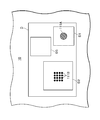
- FIG. 7 is a plan view showing an example of a circuit board 10 on which such an integrated circuit device 5 is mounted.
- a region D indicates a region where the integrated circuit device 5 is disposed.
- Regions D1, D2, and D3 indicate the positions of a plurality of IC chips included in the integrated circuit device 5, respectively.
- heat transfer paths 111 ⁇ / b> A and 111 ⁇ / b> B that connect the integrated circuit device 5 and the heat sink 21 are formed.
- the positions of the heat transfer paths 111A and 111B correspond to the positions of the IC chips that the integrated circuit device 5 has.
- the heat transfer paths 111A and 111B are located in the regions D1 and D2, respectively. By doing so, the IC chip included in the integrated circuit device 5 can be effectively cooled.
- the shapes of the heat conduction paths 111A and 111B may not be the same.
- the shapes of the heat conduction paths 111 ⁇ / b> A and 111 ⁇ / b> B may be appropriately changed according to the position of each IC chip and the circuit pattern 15 formed on the circuit board 10.
- the heat conduction path may not be provided for some IC chips included in the integrated circuit device 5.
- a heat conduction path may not be provided for an IC chip that generates a small amount of heat.
- no heat transfer path is provided for the IC chip disposed in the region D3.
- the heat sink 21 is disposed on the lower surface of the circuit board 10.
- the circuit board 10 has through holes h1 and h3 penetrating the circuit board 10 in a region A in which the integrated circuit device 5 is disposed.
- Heat conduction paths 11, 111, 111A, and 111B are provided in the through holes h1 and h3.
- the heat conduction paths 11, 111, 111A, and 111B connect the integrated circuit device 5 and the heat sink 21, and the heat of the integrated circuit device 5 is transmitted to the heat sink 21 through the heat conduction paths 11, 111, 111A, and 111B. .
- the heat conduction paths 11, 111, 111 ⁇ / b> A, 111 ⁇ / b> B are formed of a material having a higher thermal conductivity than the base material 10 a of the circuit board 10. According to this structure of the electronic devices 1 and 100, the degree of freedom can be increased with respect to the layout of other components included in the electronic device. Unlike the examples of the electronic devices 1 and 100, when another heat radiating device is arranged on the upper surface of the integrated circuit device 5, the integrated circuit device 5 is provided with two heat radiating devices, so that the cooling performance is improved. it can.
Landscapes
- Engineering & Computer Science (AREA)
- Microelectronics & Electronic Packaging (AREA)
- Physics & Mathematics (AREA)
- Thermal Sciences (AREA)
- Manufacturing & Machinery (AREA)
- Structure Of Printed Boards (AREA)
- Cooling Or The Like Of Semiconductors Or Solid State Devices (AREA)
- Cooling Or The Like Of Electrical Apparatus (AREA)
Abstract
回路基板(10)の下面にはヒートシンク(21)が配置されている。回路基板(10)は、集積回路装置(5)が配置される領域(A)内に、回路基板(10)を貫通している貫通孔(h1)を有している。この貫通孔(h1)には熱伝導路(11)が設けられている。熱伝導路(11)は集積回路装置5とヒートシンク(21)とを接続している。この構造によれば、ヒートシンク(21)とは異なる部品を集積回路装置(5)と同じ側には配置することができるので、部品のレイアウトについて自由度を増やすことができる。
Description
本発明は電子機器が有している発熱部品のための冷却構造に関する。
電子機器のなかには、CPUやGPUなどの集積回路装置にヒートシンクやヒートパイプなどの放熱装置を接続しているものがある。従来の電子機器では、回路基板の上側に集積回路装置を配置し、集積回路装置の上側に放熱装置が配置されている(例えば、特開2013-222275号公報)。
従来の電子機器では、放熱装置が他の部品のレイアウトの制約となる場合や、十分な冷却性能を得るために冷却構造が大型化してしまう場合があった。
本開示で提案する電子機器は、電子部品が配置される第1の面と、前記第1の面とは反対側の第2の面と、前記電子部品が配置される領域内に形成されている貫通孔とを有している回路基板と、前記回路基板の前記第2の面に配置され、且つ前記回路基板を挟んで前記電子部品とは反対側に位置している放熱装置と、前記回路基板の前記貫通孔に設けられ、前記電子部品と前記放熱装置とを接続する熱伝導路と、を有している。この電子機器によれば、電子機器が備えている部品のレイアウトについて自由度を増したり、或いは、電子部品のための冷却性能を向上できる。
以下、本開示で提案する電子機器の実施形態について説明する。以下の説明では、図1のZ1及びZ2が示す方向をそれぞれ上方及び下方と称する。以下の説明にある上方、下方、上側、下側などの用語は、電子機器が有している部品、部材、及び要素の相対的な位置関係を示すために使用されている。これらの用語は、電子機器内における部品等の姿勢や、電子機器の姿勢を限定するものではない。
図1に示すように、電子機器1は回路基板10を有している。回路基板10は、例えば紙フェノールやガラスエポキシ樹脂などの絶縁材料で形成された基材10aを有している。基材10aに回路パターン15(図2A参照)が形成されている。回路基板10は複数の層を有する多層基板であり、各層に回路パターン15が形成されている。回路基板10は多層基板でなくてもよい。例えば、回路基板10はその上面と下面とにだけ回路パターン15が形成された両面基板でもよいし、上面(集積回路装置などの部品が実装される面)だけに回路パターン15が形成された片面基板でもよい。
電子機器1の例では、図2Aに示すように、回路基板10は複数の回路パターン15を相互に接続する孔h2を有している(以下では、この孔h2を「接続孔」)。接続孔h2の内側には導体13が形成されており、複数の回路パターン15はこの導体13を介して相互に電気的に接続している。例えば、接続孔h2の内側には金属メッキが施される。電子機器1の例では、導体13は筒状であるが、それとは異なり、接続孔h2を埋めるように形成されてもよい。接続孔h2は、図2Aに示すように、例えば回路基板10を貫通する貫通孔である。これとは異なり、接続孔h2は回路基板10を貫通しない凹部であってもよい。回路基板10は、後述する熱伝導路11を形成するための貫通孔h1を、さらに有している。
図1に示すように、回路基板10の上面(第1の面)には電子部品が配置されている。電子部品は、例えば動作時に熱を発する発熱部品である。電子機器1の例では、回路基板10には発熱部品である集積回路装置5が配置されている。集積回路装置5は、例えばマイクロプロセッサや、メモリ、アナログ信号処理回路などであるが、これらに限定されない。また、集積回路装置5は、複数のICチップ(シリコンダイ)を1つのパッケージ内に封止したSip(system in package)でもよい。この場合、集積回路装置5は、複数のICチップが水平に並べられるSipでもよいし、複数のICチップが上下方向で並ぶSipでもよい。図1の例では、集積回路装置5は上下方向で重ねられている2つのICチップ5c、5dを有している。回路基板10には、集積回路装置5に代えて、温度の影響を受けやすい電子部品が配置されてもよい。そのような電子部品の例は、センサ類、LED(Light Emitting Diode)、インバータ、モーター類などであってもよい。
集積回路装置5は表面実装型であり、回路基板10の表面に形成されている電極パッド16(図2B参照)に接続される複数の端子を有している。電子機器1の例では、集積回路装置5はBGA(Ball Grid Array)型であり、その下面に複数の半田ボール5b(図1参照)を有している。半田ボール5bは電極パッド6にそれぞれ接続している。なお、集積回路装置5はBGA型でなくてもよい。例えば、集積回路装置5は、半田ボールに変えて、集積回路装置5の外周縁に、回路基板10に接続される複数のリード端子を有してもよい。さらに他の例では、集積回路装置5は、回路基板10に形成された孔に差し込まれて半田付けされる端子を有する挿入実装型でもよい。
回路基板10の下面(第2の面)には放熱装置が配置される。図1に示すように、電子機器1の例では、回路基板10の下面にはヒートシンク21が配置されている。ヒートシンク21は回路基板10を挟んで集積回路装置5とは反対側に位置している。すなわち、回路基板10の平面視において、ヒートシンク21は集積回路装置5と重なるように配置されている。回路基板10は、集積回路装置5が配置される領域A内に、回路基板10を貫通している貫通孔h1(図2A参照)を有している。領域Aは集積回路装置5の外形寸法に対応したサイズの領域である。すなわち、領域Aは集積回路装置5の直下の領域を意味している。言い換えれば、領域Aは、回路基板10の平面において集積回路装置5と重なる領域である。貫通孔h1は、回路基板10の上面から下面まで続いている。この貫通孔h1には熱伝導路11が設けられている。電子機器1の例では、回路基板10には、領域A内に複数の貫通孔h1が形成され、各貫通孔h1に熱伝導路11が設けられている。熱伝導路11は集積回路装置5とヒートシンク21とを接続しており、集積回路装置5の熱は熱伝導路11を介してヒートシンク21に伝えられる。熱伝導路11は、回路基板10の基材10aよりも高い熱伝導率を有する材料で形成されている。
電子機器1のこの構造によると、図1に示すように、集積回路装置5の上側には放熱装置のためのスペースが必要なくなるので、電子機器1が有する他の部品9(例えば、アンテナなどを有する送受信モジュールや、センサー、外部記憶装置など)を集積回路装置5の上側に配置でき、部品9のレイアウトについて自由度を増すことができる。電子機器1の例では、回路基板10と集積回路装置5とを挟んでヒートシンク21とは反対側に部品9が配置されている。つまり、部品9は集積回路装置5の上側に近い位置に配置されている。具体的には、部品9と集積回路装置5との距離L1は、ヒートシンク21の高さH1よりも小さい。電子機器1の例とは異なり、集積回路装置5の上面に別の放熱装置を配置してもよい。こうすることによって集積回路装置5に2つの放熱装置が設けられることとなるので、冷却性能を向上できる。
ヒートシンク21は回路基板10に取り付けられる。ヒートシンク21は、例えば回路基板10に螺子やボルトなどの固定具で固定される。ヒートシンク21は回路基板10に半田付けされてもよい。
なお、回路基板10の下面には、ヒートシンク21に代えて、或いはヒートシンク21とともに、ヒートパイプが放熱装置として配置されてもよい。そして、熱伝導路11はヒートパイプと集積回路装置5とを接続してもよい。
上述したように、回路基板10は電気回路を有している。電気回路は、上述した回路パターン15と接続孔h2の導体13とによって構成されている。熱伝導路11は、例えば導体13と同じ材料で形成される。この場合、回路基板10の製造において、導体13と同じプロセス(めっき工程)において熱伝導路11を形成することが可能となる。熱伝導路11は、回路パターン15の材料と同じ材料で形成されてもよい。この場合、回路基板10の製造において、回路パターン15と同じプロセスにおいて熱伝導路11を形成することが可能となる。なお、導体13と回路パターン15は同じ材料で形成されてもよい。回路パターン15と導体13と熱伝導路11の材料は、例えば銅である。
熱伝導路11は、電気回路の材料とは異なる材料で形成されてもよい。例えば、熱伝導路11は、電気回路の材料よりも高い電気抵抗を有する材料で形成されてもよい。こうすることによって、熱伝導路11やそれに接続されるヒートシンク21が、電磁輻射ノイズ(Electronic Magnetic Interference、EMI)の原因となることを防ぐことができる。回路パターン15は、導体材料(例えば銅)で形成され、熱伝導路11は、例えば銅よりも電気抵抗の高い金属で形成される。熱伝導路11は絶縁材料で形成されてもよい。例えば、熱伝導路11は熱伝導グリス(「放熱グリス」とも言う)で形成されてもよい。熱伝導グリスは、高い熱伝導性を有するフィラー(例えば、銅や、銀、アルミなどの粒子)が混ぜられた、シリコーン等のグリスである。熱伝導グリスは貫通孔h1に充填され、熱伝導路11を形成する。
図2Aに示すように、電子機器1の例では、熱伝導路11の材料は貫通孔h1を埋めており、熱伝導路11は柱状である。こうすることによって、集積回路装置5の熱をヒートシンク21に効率的に伝えることができる。熱伝導路11の構造は、図2Aの例に限られない。図3は熱伝導路11の他の例を示す図である(図3において図2Aと同じ箇所には同じ符号を付している)。図3に示すように、熱伝導路11は貫通孔h1の内面に沿って形成された筒状でもよい。
図2A及び図3で例示する熱伝導路11は、例えば、回路基板10の製造においてなされるめっき処理で形成され得る。熱伝導路11は、例えば、接続孔h2の導体13を形成するためのめっき処理において形成され得る。熱伝導路11の形成方法は、めっき処理に限られない。例えば、熱伝導路11は回路基板10の製造とは別個に形成されたピンでもよい。他の例では、上述したように、熱伝導グリスが貫通孔h1に挿入されて、熱伝導路11を形成してもよい。さらに他の例では、熱伝導路11は、ヒートシンク21と一体的に形成されてもよい。すなわち、ヒートシンク21の一部が貫通孔h1に挿入されて、この一部が熱伝導路11として機能してもよい。
図2Bに示すように、貫通孔h1は、回路基板10の平面視において、例えば円形である。こうすると、例えば貫通孔h1が四角形である場合に比して、回路基板10の製造において比較的容易に貫通孔h1を形成できる。なお、貫通孔h1の形状は、円形に限られない。例えば、貫通孔h1は、回路基板10の平面視において長孔でもよい。
上述したように、回路基板10には、複数の回路パターン15を接続するための接続孔h2が形成されている。図2Aに示すように、貫通孔h1の幅W1(直径)は、接続孔h2の幅(直径)W2よりも大きくてもよい。こうすることによって、集積回路装置5からヒートシンク21への熱伝達効率を向上できる。
貫通孔h1のサイズは、図2Aの例に限られない。例えば、図3に示すように、貫通孔h1の幅W1(直径)は、接続孔h2の幅(直径)W2と実質的に同じでもよい。こうすることによって、回路基板10の製造において、接続孔h2と貫通孔h1とを形成する穴開け工程において同じ工具を使用することが可能となり、回路基板10の製造を簡単化できる。図3に示す接続孔h2は回路基板10を貫通していない。接続孔h2は回路基板10の内部に形成される2つの回路パターン15を接続している。
上述したように、回路基板10には複数の貫通孔h1が形成されている。図2Bの例では、複数の貫通孔h1はグリッド状に配置されている。つまり、複数の貫通孔h1は、縦方向及び横方向に等間隔で並んでいる。図2Aに示すように、隣り合う2つの貫通孔h1の間には、回路パターン15の一部を構成する電線15cが形成されてもよい。言い換えれば、貫通孔h1は、回路パターン15の電線を避けるようにしてレイアウトされてもよい。
図4は、熱伝導路11の変形例を示す平面図である。この図の例では、回路基板10は複数の熱伝導路11A、11B、11Cを有している。隣り合う2つの熱伝導路11A、11B、11Cの間に、回路パターン15の一部を構成する電線15aが形成されている。熱伝導路11A、11B、11Cは、回路基板10の平面視において、形状及び/又はサイズが異なっている。具体的には、熱伝導路11A、11Cは長方形であるのに対して、熱伝導路11BはL字形状である。熱伝導路11Bは電線15aに合わせて屈曲している。各熱伝導路11A、11B、11Cの形状は回路パターン15の形状に合わせて適宜変更されてよい。また、各熱伝導路11A、11B、11Cの端部11a(貫通孔h1の端部)は円弧状に形成されてもよい。こうすれば例えば、熱伝導路11A、11B、11Cが形成される貫通孔h1の形成が容易となる。
図1に示すように、集積回路装置5は、その下面に、熱伝導パッド5aを有している。集積回路装置5の例では、半田ボール5bは熱伝導パッド5aの外側に形成されているが、熱伝導パッド5aの位置はこれに限られない。熱伝導パッド5aは、集積回路装置5の底面視において、半田ボール5bなど、信号の送受に利用される端子よりも大きなサイズを有する。熱伝導路11は、集積回路装置5の熱伝導パッド5aに接続している。電子機器1の例では、複数の熱伝導路11が熱伝導パッド5aの領域B(図2B参照)内に位置し、熱伝導パッド5aに接続している。熱伝導パッド5aは、例えば金属で形成される。
熱伝導パッド5aは回路基板10との電気的接続に利用されてもよい。例えば、熱伝導パッド5aはグランド線として利用されてもよい。つまり、熱伝導路11が導体である場合、熱伝導路11は回路基板10に形成されているグランド線に接続し、熱伝導路11と熱伝導パッド5aは、電気的及び熱的に、互いに接続されてよい。このような例とは異なり、熱伝導パッド5aは回路基板10との電気的接続に利用されていなくてもよい。つまり、熱伝導路11と熱伝導パッド5aは、回路基板10の回路から電気的に独立していてもよい。
図1に示すように、熱伝導パッド5aと熱伝導路11との間には、これらを熱的に接続する接続部材31が配置されてもよい。熱伝導パッド5aと熱伝導路11の双方が金属で形成される場合、接続部材31は例えば半田である。すなわち、熱伝導パッド5aと熱伝導路11の双方が金属で形成される場合、これらは、例えば半田によって、電気的且つ熱的に互いに接続される。接続部材31は半田に限られない。例えば、接続部材31は熱伝導グリス(「放熱グリス」とも言う)でもよいし、熱伝導シートでもよい。接続部材31は、熱伝導路11と熱伝導パッド5aの公差を吸収できるように変形可能であれば、必ずしも熱伝導グリスや熱伝導シートに限られない。
図1に示すように、ヒートシンク21と熱伝導路11との間には、それらを熱的に接続する接続部材32が配置されてもよい。接続部材32は、例えば熱伝導シートである。この熱伝導シートは回路基板10の厚さ方向での弾性を有する。こうすることによって、ヒートシンク21と熱伝導路11との接続安定性を確保でき、また、ヒートシンク21を回路基板10に押しつけたときに、その力が集積回路装置5に及ぶことを抑えることができる。熱伝導シートとしては、シリコーンを含むものや、アクリル樹脂を含むものなどを利用できる。接続部材32は、上述した熱伝導グリスでもよい。この場合でも、ヒートシンク21と熱伝導路11との接続安定性を確保できる。
図5は、回路基板10の変形例を示す図である(この図において、図2Aと同一の箇所には同一符号を付している)。この図の例において、回路基板10は、その下面(ヒートシンク21に向いた面)に、金属層18を有している。金属層18は、例えば複数の貫通孔h1が形成されている領域全体に亘って形成され、複数の熱伝導路11を接続している。回路基板10が金属層18を有する場合、ヒートシンク21はこの金属層18に接続する。この場合、ヒートシンク21は金属層18に直接的に接触してもよいし、ヒートシンク21と金属層18との間に、上述した熱伝導シートや熱伝導グリスなどである接続部材32が配置されてもよい。金属層18は、例えば、回路パターン15と同じ材料で形成される。これによって、金属層18と、回路パターン15(具体的には、回路基板10の下面に形成される回路パターン15)は、回路基板10の製造において、同じ工程で形成できる。
なお、図5の例では、回路基板10の上面にも、複数の熱伝導路11を接続する金属層17が形成されている。金属層17は、例えば複数の貫通孔h1が形成されている領域全体に亘って形成され、複数の熱伝導路11を接続している。回路基板10が金属層17を有する場合、集積回路装置5の熱伝導パッド5aはこの金属層17に接続する。この場合、熱伝導パッド5aは、金属層17に半田付けされてもよい。それとは異なり、熱伝導パッド5aと金属層17との間に、上述した熱伝導シートや熱伝導グリスなどである接続部材31が配置されてもよい。金属層17は、例えば、回路パターン15と同じ材料で形成される。これによって、金属層17と、回路パターン15(具体的には、回路基板10の上面に形成される回路パターン15)は、回路基板10の製造において、同じ工程で形成できる。
図6は、熱伝導路11の変形例を示す断面図である。この図において、図1と同一の箇所には同一符号を付している。この図に示す電子機器100の例では、回路基板10は1つの貫通孔h3を有している。貫通孔h3は、上述した接続孔h2の幅W2よりも大きな幅W3を有している。より具体的には、幅W3は、2つの半田ボール5bの間隔W4よりもさらに大きい。幅W3は、集積回路装置5が熱伝導パッド5aのサイズの半分よりも大きい。幅W3は、集積回路装置5が熱伝導パッド5aの幅に実質的に対応してもよい。熱伝導路111は貫通孔h3に充填されている。すなわち、熱伝導路11は貫通孔h3の全域に形成されている。このような比較的大きな貫通孔h3を形成すれば、集積回路装置5の熱をさらに効率的にヒートシンク21に伝えることができる。
上述したように、集積回路装置5は、複数のICチップ(シリコンダイ)を1つのパッケージ内に封止したSipでもよい。図7は、そのような集積回路装置5が実装される回路基板10の例を示す平面図である。この図において領域Dは、集積回路装置5が配置される領域を示している。領域D1、D2、D3は、それぞれ集積回路装置5が有している複数のICチップの位置を示している。回路基板10には、集積回路装置5とヒートシンク21とを接続する熱伝達路111A、111Bが形成されている。熱伝達路111A、111Bの位置は、集積回路装置5が有しているICチップの位置に対応している。すなわち、熱伝達路111A、111Bは領域D1、D2にそれぞれ位置している。こうすることによって、集積回路装置5が有するICチップを効果的に冷却できる。熱伝導路111A、111Bの形状は同じで無くてもよい。熱伝導路111A、111Bの形状は、各ICチップの位置や、回路基板10に形成される回路パターン15に合わせて適宜変更されてよい。
なお、熱伝導路は、集積回路装置5が有する一部のICチップについては設けられていなくてもよい。例えば、発熱量が小さいICチップに対しては、熱伝導路は設けられていなくてもよい。図7の例では、領域D3に配置されるICチップについて、熱伝達路は設けられていない。
以上説明したように、電子機器1、100の例では、回路基板10の下面にはヒートシンク21が配置されている。回路基板10は、集積回路装置5が配置される領域A内に、回路基板10を貫通している貫通孔h1、h3を有している。この貫通孔h1、h3には熱伝導路11、111、111A、111Bが設けられている。熱伝導路11、111、111A、111Bは集積回路装置5とヒートシンク21とを接続しており、集積回路装置5の熱は熱伝導路11、111、111A、111Bを介してヒートシンク21に伝えられる。熱伝導路11、111、111A、111Bは、回路基板10の基材10aよりも高い熱伝導率を有する材料で形成されている。電子機器1、100のこの構造によると、電子機器が有している他の部品のレイアウトについて自由度を増すことができる。電子機器1、100の例とは異なり、集積回路装置5の上面に別の放熱装置を配置する場合には、集積回路装置5に2つの放熱装置が設けられることとなるので、冷却性能を向上できる。
なお、本発明は以上説明した実施形態に限られず、種々の変更がなされてよい。
Claims (14)
- 電子部品が配置される第1の面と、前記第1の面とは反対側の第2の面と、前記電子部品が配置される領域内に形成されている貫通孔とを有している回路基板と、
前記回路基板の前記第2の面に配置され、且つ前記回路基板を挟んで前記電子部品とは反対側に位置している放熱装置と、
前記回路基板の前記貫通孔に設けられ、前記電子部品と前記放熱装置とを接続する熱伝導路と、を有している
ことを特徴とする電子機器。 - 前記回路基板には、前記領域内に位置する複数の貫通孔が形成され、
前記複数の貫通孔のそれぞれに前記熱伝導路が設けられている
ことを特徴とする請求項1に記載の電子機器。 - 前記回路基板は回路パターンを有し、
前記複数の貫通孔のうち隣接する2つの貫通孔の間に、前記回路パターンを構成する電線が形成されている
ことを特徴とする請求項2に記載の電子機器。 - 前記回路基板は、複数の層と、複数の層にそれぞれ形成されている複数の回路パターンと、前記回路基板を貫通し且つ前記複数の回路パターンを電気的に接続する孔である接続孔とを有し、
前記貫通孔のサイズは、平面視において、前記接続孔よりも大きい
ことを特徴とする請求項1に記載の電子機器。 - 前記回路基板は、複数の層と、複数の層にそれぞれ形成されている複数の回路パターンと、前記回路基板を貫通し且つ前記複数の回路パターンを電気的に接続する接続孔とを有し、
前記貫通孔のサイズは、平面視において、前記接続孔と実質的に同じである
ことを特徴とする請求項1に記載の電子機器。 - 前記電子部品は集積回路装置であり、
前記集積回路装置は、前記回路基板に向いてる面に熱伝導部を有し、
前記貫通孔のサイズは、前記回路基板の平面視において、前記熱伝導部の半分よりも大きい
ことを特徴とする請求項1に記載の電子機器。 - 前記回路基板には電気回路が形成されており、
前記熱伝導路は前記電気回路の材料よりも電気抵抗が高い材料で形成されている
ことを特徴とする請求項1に記載の電子機器。 - 前記回路基板には電気回路が形成されており、
前記熱伝導路は前記電気回路の材料と同じ材料で形成されている
ことを特徴とする請求項1に記載の電子機器。 - 前記熱伝導路は前記貫通孔の内側に形成されるめっきである
ことを特徴とする請求項1に記載の電子機器。 - 前記電子部品は集積回路装置であり、
前記集積回路装置は、前記回路基板に向いてる面に熱伝導部を有し、
前記熱伝導路は前記熱伝導部に接続している
ことを特徴とする請求項1に記載の電子機器。 - 前記放熱部材と前記熱伝導路との間には、熱伝導シートと熱伝導グリスのうち少なくとも一方が配置されている
ことを特徴とする請求項1に記載の電子機器。 - 前記回路基板は、前記第2の面に、前記貫通孔の前記熱伝導路に接続され且つ前記回路基板と一体に形成されている金属層を有している
ことを特徴とする請求項1に記載の電子機器。 - 前記回路基板と前記電子部品とを挟んで前記放熱装置とは反対側に、別の部品が配置されている
前記別の部品と前記電子部品との距離は、前記回路基板の厚さ方向での前記放熱装置の厚さよりも小さい
ことを特徴とする請求項1に記載の電子機器。 - 前記熱伝導路は、前記回路基板の基材よりも高い熱伝導率を有する材料で形成され、且つ前記貫通孔を満たしている
ことを特徴とする請求項1に記載の電子機器。
Priority Applications (3)
| Application Number | Priority Date | Filing Date | Title |
|---|---|---|---|
| JP2019520224A JP6891274B2 (ja) | 2017-05-22 | 2018-05-18 | 電子機器 |
| US16/612,509 US11393737B2 (en) | 2017-05-22 | 2018-05-18 | Electronic equipment |
| CN201880032381.8A CN110637361B (zh) | 2017-05-22 | 2018-05-18 | 电子设备 |
Applications Claiming Priority (2)
| Application Number | Priority Date | Filing Date | Title |
|---|---|---|---|
| JP2017101257 | 2017-05-22 | ||
| JP2017-101257 | 2017-05-22 |
Publications (1)
| Publication Number | Publication Date |
|---|---|
| WO2018216627A1 true WO2018216627A1 (ja) | 2018-11-29 |
Family
ID=64396439
Family Applications (1)
| Application Number | Title | Priority Date | Filing Date |
|---|---|---|---|
| PCT/JP2018/019358 Ceased WO2018216627A1 (ja) | 2017-05-22 | 2018-05-18 | 電子機器 |
Country Status (4)
| Country | Link |
|---|---|
| US (1) | US11393737B2 (ja) |
| JP (1) | JP6891274B2 (ja) |
| CN (1) | CN110637361B (ja) |
| WO (1) | WO2018216627A1 (ja) |
Cited By (3)
| Publication number | Priority date | Publication date | Assignee | Title |
|---|---|---|---|---|
| WO2021010173A1 (ja) * | 2019-07-12 | 2021-01-21 | ソニーセミコンダクタソリューションズ株式会社 | 配線モジュール及び撮像装置 |
| JP2022155786A (ja) * | 2021-03-31 | 2022-10-14 | 日立Astemo株式会社 | 電子装置 |
| TWI884454B (zh) * | 2022-06-10 | 2025-05-21 | 新加坡商星科金朋私人有限公司 | 與半導體裝置一起使用的散熱器 |
Families Citing this family (7)
| Publication number | Priority date | Publication date | Assignee | Title |
|---|---|---|---|---|
| KR102812686B1 (ko) * | 2020-06-22 | 2025-05-27 | 엘지이노텍 주식회사 | 통신 모듈 |
| CN111954370B (zh) * | 2020-08-24 | 2021-08-10 | 浙江集迈科微电子有限公司 | Pcb板微流道散热嵌入结构 |
| CN117178643A (zh) * | 2021-04-09 | 2023-12-05 | 株式会社村田制作所 | 包括氮化镓器件的电路组件 |
| JP7675595B2 (ja) * | 2021-08-18 | 2025-05-13 | 三菱電機株式会社 | 半導体モジュール |
| JP2024545810A (ja) * | 2021-12-22 | 2024-12-12 | テレフオンアクチーボラゲット エルエム エリクソン(パブル) | 集積回路のための熱相互接続 |
| DE102023136151A1 (de) * | 2023-12-20 | 2025-06-26 | Sma Solar Technology Ag | Platte, leistungshalbleiteranordnung und verfahren zum herstellen einer leistungshalbleiteranordnung |
| EP4626154A1 (en) * | 2024-03-28 | 2025-10-01 | Dab Pumps S.p.A. | Electronic input/output apparatus with improved dissipation |
Citations (7)
| Publication number | Priority date | Publication date | Assignee | Title |
|---|---|---|---|---|
| JPH0982857A (ja) * | 1995-09-18 | 1997-03-28 | Nec Corp | マルチチップパッケージ構造 |
| JP2001284748A (ja) * | 2000-03-29 | 2001-10-12 | Rohm Co Ltd | 放熱手段を有するプリント配線板およびその製造方法 |
| JP2002118384A (ja) * | 2000-08-01 | 2002-04-19 | Mitsubishi Electric Corp | 電子機器 |
| JP2013105904A (ja) * | 2011-11-14 | 2013-05-30 | Renesas Electronics Corp | 半導体装置 |
| JP2014036033A (ja) * | 2012-08-07 | 2014-02-24 | Hitachi Automotive Systems Ltd | 半導体装置 |
| JP2015133373A (ja) * | 2014-01-10 | 2015-07-23 | 株式会社デンソー | 回路基板および電子装置 |
| JP2016111117A (ja) * | 2014-12-04 | 2016-06-20 | オムロンオートモーティブエレクトロニクス株式会社 | 回路基板、回路基板の放熱構造、回路基板の製造方法 |
Family Cites Families (25)
| Publication number | Priority date | Publication date | Assignee | Title |
|---|---|---|---|---|
| US5920458A (en) * | 1997-05-28 | 1999-07-06 | Lucent Technologies Inc. | Enhanced cooling of a heat dissipating circuit element |
| DE19842590A1 (de) * | 1998-09-17 | 2000-04-13 | Daimler Chrysler Ag | Verfahren zur Herstellung von Schaltungsanordnungen |
| US6696643B2 (en) * | 2000-08-01 | 2004-02-24 | Mitsubishi Denki Kabushiki Kaisha | Electronic apparatus |
| US6477054B1 (en) * | 2000-08-10 | 2002-11-05 | Tektronix, Inc. | Low temperature co-fired ceramic substrate structure having a capacitor and thermally conductive via |
| US6373348B1 (en) * | 2000-08-11 | 2002-04-16 | Tektronix, Inc. | High speed differential attenuator using a low temperature co-fired ceramic substrate |
| JP2003289191A (ja) * | 2002-03-28 | 2003-10-10 | Denso Corp | 電子制御装置 |
| JP2004172459A (ja) * | 2002-11-21 | 2004-06-17 | Advics:Kk | 電子制御装置における電子部品の放熱構造 |
| JP4457694B2 (ja) * | 2003-05-19 | 2010-04-28 | 株式会社デンソー | 電子部品の放熱構造 |
| US7054156B2 (en) | 2003-09-02 | 2006-05-30 | Hewlett-Packard Development Company, L.P. | Fan rotor systems having collapsible fan blades |
| US7253518B2 (en) * | 2005-06-15 | 2007-08-07 | Endicott Interconnect Technologies, Inc. | Wirebond electronic package with enhanced chip pad design, method of making same, and information handling system utilizing same |
| US20080080142A1 (en) * | 2006-09-28 | 2008-04-03 | Mediatek Inc. | Electronic devices with enhanced heat spreading |
| JP2008140924A (ja) * | 2006-11-30 | 2008-06-19 | Toshiba Corp | 電子機器 |
| US7808788B2 (en) * | 2007-06-29 | 2010-10-05 | Delphi Technologies, Inc. | Multi-layer electrically isolated thermal conduction structure for a circuit board assembly |
| DE102007037297A1 (de) * | 2007-08-07 | 2009-02-19 | Continental Automotive Gmbh | Schaltungsträgeraufbau mit verbesserter Wärmeableitung |
| US7974099B2 (en) * | 2007-11-19 | 2011-07-05 | Nexxus Lighting, Inc. | Apparatus and methods for thermal management of light emitting diodes |
| JP2013077781A (ja) * | 2011-09-30 | 2013-04-25 | Fujitsu Ltd | 電子機器 |
| JP5971751B2 (ja) | 2012-04-13 | 2016-08-17 | 株式会社ソニー・インタラクティブエンタテインメント | 電子機器 |
| JP5579234B2 (ja) * | 2012-08-30 | 2014-08-27 | 三菱電機株式会社 | 電子回路部品の冷却構造及びそれを用いたインバータ装置 |
| TW201505532A (zh) * | 2013-07-26 | 2015-02-01 | Jitboundary United Production Inc | 高散熱電路板組 |
| JP6164304B2 (ja) * | 2013-11-28 | 2017-07-19 | 富士電機株式会社 | 半導体モジュール用冷却器の製造方法、半導体モジュール用冷却器、半導体モジュール及び電気駆動車両 |
| DE102015210099B4 (de) * | 2015-02-10 | 2022-12-01 | Vitesco Technologies Germany Gmbh | Elektronische Komponente und Verfahren zur Herstellung einer solchen elektronischen Komponente |
| WO2017094589A1 (ja) * | 2015-11-30 | 2017-06-08 | 日本精工株式会社 | 放熱基板及び電動パワーステアリング装置 |
| US10050014B2 (en) * | 2016-02-22 | 2018-08-14 | Taiyo Yuden Co., Ltd. | Circuit substrate and method of manufacturing same |
| DE102018109920A1 (de) * | 2018-04-25 | 2019-10-31 | Dr. Ing. H.C. F. Porsche Aktiengesellschaft | Kühlung von leistungselektronischen Schaltungen |
| US11121096B2 (en) * | 2019-03-21 | 2021-09-14 | International Business Machines Corporation | Active control of electronic package warpage |
-
2018
- 2018-05-18 CN CN201880032381.8A patent/CN110637361B/zh active Active
- 2018-05-18 US US16/612,509 patent/US11393737B2/en active Active
- 2018-05-18 WO PCT/JP2018/019358 patent/WO2018216627A1/ja not_active Ceased
- 2018-05-18 JP JP2019520224A patent/JP6891274B2/ja active Active
Patent Citations (7)
| Publication number | Priority date | Publication date | Assignee | Title |
|---|---|---|---|---|
| JPH0982857A (ja) * | 1995-09-18 | 1997-03-28 | Nec Corp | マルチチップパッケージ構造 |
| JP2001284748A (ja) * | 2000-03-29 | 2001-10-12 | Rohm Co Ltd | 放熱手段を有するプリント配線板およびその製造方法 |
| JP2002118384A (ja) * | 2000-08-01 | 2002-04-19 | Mitsubishi Electric Corp | 電子機器 |
| JP2013105904A (ja) * | 2011-11-14 | 2013-05-30 | Renesas Electronics Corp | 半導体装置 |
| JP2014036033A (ja) * | 2012-08-07 | 2014-02-24 | Hitachi Automotive Systems Ltd | 半導体装置 |
| JP2015133373A (ja) * | 2014-01-10 | 2015-07-23 | 株式会社デンソー | 回路基板および電子装置 |
| JP2016111117A (ja) * | 2014-12-04 | 2016-06-20 | オムロンオートモーティブエレクトロニクス株式会社 | 回路基板、回路基板の放熱構造、回路基板の製造方法 |
Cited By (5)
| Publication number | Priority date | Publication date | Assignee | Title |
|---|---|---|---|---|
| WO2021010173A1 (ja) * | 2019-07-12 | 2021-01-21 | ソニーセミコンダクタソリューションズ株式会社 | 配線モジュール及び撮像装置 |
| US11882646B2 (en) | 2019-07-12 | 2024-01-23 | Sony Semiconductor Solutions Corporation | Wiring module and imaging apparatus |
| JP2022155786A (ja) * | 2021-03-31 | 2022-10-14 | 日立Astemo株式会社 | 電子装置 |
| JP7542183B2 (ja) | 2021-03-31 | 2024-08-30 | 日立Astemo株式会社 | 電子装置 |
| TWI884454B (zh) * | 2022-06-10 | 2025-05-21 | 新加坡商星科金朋私人有限公司 | 與半導體裝置一起使用的散熱器 |
Also Published As
| Publication number | Publication date |
|---|---|
| US11393737B2 (en) | 2022-07-19 |
| JP6891274B2 (ja) | 2021-06-18 |
| CN110637361A (zh) | 2019-12-31 |
| JPWO2018216627A1 (ja) | 2019-12-12 |
| CN110637361B (zh) | 2024-04-19 |
| US20200126884A1 (en) | 2020-04-23 |
Similar Documents
| Publication | Publication Date | Title |
|---|---|---|
| JP6891274B2 (ja) | 電子機器 | |
| US10204848B2 (en) | Semiconductor chip package having heat dissipating structure | |
| US8213180B2 (en) | Electromagnetic interference shield with integrated heat sink | |
| EP3310140B1 (en) | Mounting assembly with a heatsink | |
| US9271388B2 (en) | Interposer and package on package structure | |
| US20140029201A1 (en) | Power package module and manufacturing method thereof | |
| US10925148B2 (en) | Printed circuit board assembly | |
| JP2008091714A (ja) | 半導体装置 | |
| JP2006073651A (ja) | 半導体装置 | |
| JP2009283828A (ja) | 半導体装置および半導体装置の製造方法 | |
| US10068817B2 (en) | Semiconductor package | |
| JP6093093B2 (ja) | 半導体モジュール | |
| CN101322450B (zh) | 具有内部散热结构的ic封装 | |
| JP7223639B2 (ja) | 電子制御装置 | |
| JP2011146513A (ja) | 半導体装置 | |
| JP4919689B2 (ja) | モジュール基板 | |
| JP2012199283A (ja) | 半導体装置 | |
| KR101027984B1 (ko) | 히트싱크를 갖는 기판보드 어셈블리 | |
| US11798873B2 (en) | Semiconductor assembly | |
| JP3076812U (ja) | 配線板 | |
| JP2016152290A (ja) | 熱伝導基板及び電子部品実装方法 | |
| KR19990071282A (ko) | 반도체 패키지 제조방법 | |
| KR20130141175A (ko) | 칩 패키지 및 그 제조 방법 | |
| JP2016171202A (ja) | 電子装置 |
Legal Events
| Date | Code | Title | Description |
|---|---|---|---|
| 121 | Ep: the epo has been informed by wipo that ep was designated in this application |
Ref document number: 18805811 Country of ref document: EP Kind code of ref document: A1 |
|
| ENP | Entry into the national phase |
Ref document number: 2019520224 Country of ref document: JP Kind code of ref document: A |
|
| NENP | Non-entry into the national phase |
Ref country code: DE |
|
| 122 | Ep: pct application non-entry in european phase |
Ref document number: 18805811 Country of ref document: EP Kind code of ref document: A1 |