WO2018207620A1 - 蓄電素子の接続構造および蓄電モジュール - Google Patents
蓄電素子の接続構造および蓄電モジュール Download PDFInfo
- Publication number
- WO2018207620A1 WO2018207620A1 PCT/JP2018/016710 JP2018016710W WO2018207620A1 WO 2018207620 A1 WO2018207620 A1 WO 2018207620A1 JP 2018016710 W JP2018016710 W JP 2018016710W WO 2018207620 A1 WO2018207620 A1 WO 2018207620A1
- Authority
- WO
- WIPO (PCT)
- Prior art keywords
- circuit board
- electrode
- power
- pattern
- storage element
- Prior art date
- Legal status (The legal status is an assumption and is not a legal conclusion. Google has not performed a legal analysis and makes no representation as to the accuracy of the status listed.)
- Ceased
Links
Images



Classifications
-
- H—ELECTRICITY
- H01—ELECTRIC ELEMENTS
- H01G—CAPACITORS; CAPACITORS, RECTIFIERS, DETECTORS, SWITCHING DEVICES, LIGHT-SENSITIVE OR TEMPERATURE-SENSITIVE DEVICES OF THE ELECTROLYTIC TYPE
- H01G9/00—Electrolytic capacitors, rectifiers, detectors, switching devices, light-sensitive or temperature-sensitive devices; Processes of their manufacture
- H01G9/004—Details
- H01G9/008—Terminals
-
- H—ELECTRICITY
- H01—ELECTRIC ELEMENTS
- H01G—CAPACITORS; CAPACITORS, RECTIFIERS, DETECTORS, SWITCHING DEVICES, LIGHT-SENSITIVE OR TEMPERATURE-SENSITIVE DEVICES OF THE ELECTROLYTIC TYPE
- H01G2/00—Details of capacitors not covered by a single one of groups H01G4/00-H01G11/00
- H01G2/02—Mountings
- H01G2/04—Mountings specially adapted for mounting on a chassis
-
- H—ELECTRICITY
- H01—ELECTRIC ELEMENTS
- H01G—CAPACITORS; CAPACITORS, RECTIFIERS, DETECTORS, SWITCHING DEVICES, LIGHT-SENSITIVE OR TEMPERATURE-SENSITIVE DEVICES OF THE ELECTROLYTIC TYPE
- H01G11/00—Hybrid capacitors, i.e. capacitors having different positive and negative electrodes; Electric double-layer [EDL] capacitors; Processes for the manufacture thereof or of parts thereof
- H01G11/08—Structural combinations, e.g. assembly or connection, of hybrid or EDL capacitors with other electric components, at least one hybrid or EDL capacitor being the main component
-
- H—ELECTRICITY
- H01—ELECTRIC ELEMENTS
- H01G—CAPACITORS; CAPACITORS, RECTIFIERS, DETECTORS, SWITCHING DEVICES, LIGHT-SENSITIVE OR TEMPERATURE-SENSITIVE DEVICES OF THE ELECTROLYTIC TYPE
- H01G11/00—Hybrid capacitors, i.e. capacitors having different positive and negative electrodes; Electric double-layer [EDL] capacitors; Processes for the manufacture thereof or of parts thereof
- H01G11/10—Multiple hybrid or EDL capacitors, e.g. arrays or modules
-
- H—ELECTRICITY
- H01—ELECTRIC ELEMENTS
- H01G—CAPACITORS; CAPACITORS, RECTIFIERS, DETECTORS, SWITCHING DEVICES, LIGHT-SENSITIVE OR TEMPERATURE-SENSITIVE DEVICES OF THE ELECTROLYTIC TYPE
- H01G11/00—Hybrid capacitors, i.e. capacitors having different positive and negative electrodes; Electric double-layer [EDL] capacitors; Processes for the manufacture thereof or of parts thereof
- H01G11/74—Terminals, e.g. extensions of current collectors
- H01G11/76—Terminals, e.g. extensions of current collectors specially adapted for integration in multiple or stacked hybrid or EDL capacitors
-
- H—ELECTRICITY
- H01—ELECTRIC ELEMENTS
- H01G—CAPACITORS; CAPACITORS, RECTIFIERS, DETECTORS, SWITCHING DEVICES, LIGHT-SENSITIVE OR TEMPERATURE-SENSITIVE DEVICES OF THE ELECTROLYTIC TYPE
- H01G11/00—Hybrid capacitors, i.e. capacitors having different positive and negative electrodes; Electric double-layer [EDL] capacitors; Processes for the manufacture thereof or of parts thereof
- H01G11/78—Cases; Housings; Encapsulations; Mountings
- H01G11/82—Fixing or assembling a capacitive element in a housing, e.g. mounting electrodes, current collectors or terminals in containers or encapsulations
-
- H—ELECTRICITY
- H01—ELECTRIC ELEMENTS
- H01G—CAPACITORS; CAPACITORS, RECTIFIERS, DETECTORS, SWITCHING DEVICES, LIGHT-SENSITIVE OR TEMPERATURE-SENSITIVE DEVICES OF THE ELECTROLYTIC TYPE
- H01G9/00—Electrolytic capacitors, rectifiers, detectors, switching devices, light-sensitive or temperature-sensitive devices; Processes of their manufacture
- H01G9/004—Details
- H01G9/08—Housing; Encapsulation
Definitions
- the technology disclosed in this specification relates to a connection structure of a storage element and a storage module.
- Patent Document 1 Conventionally, for example, a capacitor device disclosed in Patent Document 1 is known as an auxiliary power source used for emergency when the main power source becomes unusable.
- capacitors capacitors having electrodes and safety valves for releasing abnormal pressure are accommodated in a storage case. And on the top surface, individual bus bars are arranged between the electrodes and fixed with screws, and a circuit board for controlling the balance of each storage element is fixed in the area avoiding each electrode and safety valve And is held integrally with the capacitor.
- the technology disclosed in the present specification has been completed based on the above-described circumstances, and the storage unit connection structure and the storage module that can hold the circuit board while connecting the storage elements are reduced in the number of parts. It aims at providing at low cost.
- a connection structure for connecting electrodes of a plurality of power storage elements includes a through hole through which the electrode is inserted and a power pattern, and is mounted on the plurality of power storage elements.
- the circuit board is fastened to the power storage element and the power pattern is electrically connected to the electrode simply by placing the circuit board on the electrodes of the plurality of power storage elements and screwing the fastening member to the electrode. Since it can be connected, the number of parts and man-hours can be reduced. And since the spacer is provided in the through-hole of the circuit board, the pressing force with respect to the circuit board of a fastening member can be restrict
- the power pattern includes a plurality of contact parts exposed on the surface of the circuit board, and the fastening member presses the plurality of contact parts against the electrodes of the plurality of power storage elements through the circuit board. Good.
- a conductive plating layer is formed on the inner wall of the through hole, and the power pattern is arranged on the electrode side and pressed against the electrode by the first power pattern and the first power via the insulating layer. And a second power pattern that is stacked on the power pattern and electrically connected to the first power pattern via the plating layer.
- the second power pattern formed in a layer different from the first power pattern can also be connected to the electrode. Thereby, a bigger electric current can be sent.
- the circuit board may be provided with a control circuit for controlling the state of the power storage element, and a signal pattern for connecting the power pattern and the control circuit may be formed.
- This configuration eliminates the need for an electric wire for connecting the control circuit and the electrodes, thereby reducing the number of components.
- the power storage module includes a plurality of power storage elements, a case that houses the plurality of power storage elements, a through-hole through which an electrode of each power storage element is inserted, and a power pattern.
- a circuit board a shaft portion inserted through the through-hole and screwed into the electrode of the power storage element, and the power pattern being pressed against the electrode of the power storage element through the circuit board integrated with the shaft portion And a cap disposed between the power storage element and the circuit board.
- the power storage module includes: a fastening member including a pressing portion configured to support; a spacer disposed in the through hole to support the pressing portion; and a cap disposed between the power storage element and the circuit board.
- the power storage element is provided with a safety valve that opens the internal space when the internal space exceeds a predetermined pressure, and the cap is disposed between the circuit board and the safety valve to provide the safety valve.
- a board support part for supporting the circuit board together with the electrodes may be provided on the cap so as to protrude toward the circuit board.
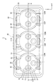
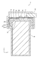
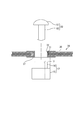
- AA sectional view of FIG. BB sectional view of FIG. Exploded front view of the connection structure between electrodes
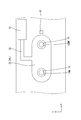
- Top view showing power and signal patterns
- Front view showing the connection structure between electrodes
- the top view which shows the electrical storage module of Embodiment 2.
- the power storage module 1 of this embodiment is mounted on a vehicle as a sub power source when the main power source becomes inoperable.
- the power storage module 1 includes a plurality of (three in the present embodiment) capacitors 10 (an example of a power storage element) accommodated in a case 60.
- the circuit board 30 is placed and fastened to the electrode 12 with a bolt 50.
- a cap 20 is disposed between the circuit board 30 and the capacitor 10.
- the circuit board 30 is arranged to electrically connect the capacitors 10 and to control the state of the capacitors 10.
- the circuit board 30 is not shown in detail, and only the outline is indicated by a two-dot chain line C.
- the case 60 has a rectangular parallelepiped shape with an upper surface opening, and a plurality of (three in the present embodiment) cylindrical capacitor housing portions 61 are provided side by side inside the case 60.
- the upper surface of each capacitor housing 61 is opened, and a pair of guide ribs 62 for positioning the cap 20 are provided along the front-rear direction, as shown in FIG. .
- Each of the capacitors 10A to 10C has a cylindrical capacitor body portion disposed in the capacitor housing portion 61, and is accommodated with the electrode 12 facing upward and the positive electrode P and the negative electrode N alternately disposed side by side. Yes.
- a safety valve 11 is provided behind the electrode 12, and is opened when the capacitor 10 becomes a predetermined internal pressure or higher due to heat generation or the like, and gas or the like is ejected from the capacitor 10.
- Each capacitor 10 is connected in series by a power pattern on a circuit board 30 to be described later, and is connected to the outside from the electrodes 12AP and 12CN at both ends via a connector 40 mounted on the board.
- each electrode 12 is integrally provided with a base portion 15 protruding from the capacitor 10 and a spacer portion 16 protruding from the base portion 15 and having a smaller diameter than the base portion 15.
- the electrode 12 has an insertion hole 13 through which the bolt 50 is inserted.
- the cap 20 includes a disc-shaped cap body 20 ⁇ / b> A and a peripheral wall portion 20 ⁇ / b> B that extends downward from the peripheral edge and surrounds the peripheral surface of the capacitor 10.
- the cap body 20 ⁇ / b> A is placed on the upper surface of the capacitor 10 with each electrode 12 inserted through the two holes 21.
- a safety cover portion 22 is provided behind the hole portion 21 and is disposed between the safety valve 11 and the circuit board 30.
- the safety cover portion 22 is formed in a shape in which the lower surface of the cap main body 20A is formed in a circular shape, and is formed one step higher than the upper surface of the cap main body 20A on the upper surface side. As a result, the safety cover portion 22 has a thickness comparable to that of the cap body 20A.
- an escape groove 23 for guiding the gas ejected from the safety valve 11 in a direction away from the circuit board 30 is provided inside the cap 20 (on the side facing the capacitor 10).
- the escape groove portion 23 includes a horizontal escape portion 23A extending rearward from the safety cover portion 22, and a vertical escape portion 23B extending downward from the rear end of the horizontal escape portion.
- the horizontal relief portion 23A is provided continuously from the safety cover portion 22, and has a shape in which the lower surface of the cap body 20A is formed in a groove shape.
- the vertical escape portion 23B is provided continuously from the rear end of the horizontal escape portion 23A, and has a shape in which the inner wall of the peripheral wall portion 20B of the cap 20 is formed in a groove shape.
- the space defined between the safety cover portion 22 and the capacitor 10 is the space defined between the horizontal escape portion 23A and the capacitor 10 and between the vertical escape portion 23B and the capacitor main body portion. It communicates with the lower space of the cap 20 through a defined space.
- the gas ejected from the safety valve 11 passes through these spaces (that is, guided in a direction away from the circuit board 30 by the safety cover portion 22 and the escape groove portion 23), and is released to the space below the cap 20. .
- a locking portion 24 extends from the front end and the rear end of the peripheral wall portion, and a locking piece provided near the front end of the peripheral wall portion is locked from the inside to a locking receiving portion provided near the upper end of the case 60.
- a pair of support ribs 25 are respectively provided along the front-rear direction and are erected upward on the front side and the rear side of the cap body 20A. And a circuit board 30 to be described later are supported.
- the circuit board 30 has a rectangular flat plate shape slightly smaller than the upper opening of the case 60 and is fitted into the case 60 and supported by the base portion 15 of the electrode 12 and the support rib 25 of the cap 20.
- a plurality (six in this embodiment) of through holes 31 are provided in the circuit board 30 side by side.
- the through-hole 31 is formed in a circular shape having a diameter slightly larger than that of the spacer portion 16 of the electrode 12 and smaller than that of the base portion 15. Spacer portions 16 are inserted into the respective through holes 31 of the circuit board 30.
- the upper surface opening of the insertion hole 13 is exposed in the spacer portion 16 disposed in the through hole 31, and a bolt 50 is inserted therein to fasten the circuit board 30 to the electrode 12.
- the bolt 50 is a well-known one that includes a head 51 (an example of a pressing portion) and a shaft portion 52 that is formed integrally with the head 51.
- the shaft portion 52 is inserted into and screwed into the electrode 12, and the head portion 51 is in contact with the upper surface of the circuit board 30 and presses it against the base portion 15 of the electrode 12. Further, the lower surface of the head 51 is also in contact with and supported by the upper surface of the spacer portion 16 of the electrode 12.
- a conductive plating layer 32 is provided on the inner peripheral surface (inner wall) of each through hole 31.
- the thickness of the plated layer 32 is not considered, and the inner peripheral surface of the plated layer 32 is described as the inner peripheral surface of the through hole 31.
- the circuit board 30 is provided with a power pattern for conducting power from the capacitor 10 and a signal pattern 36 for conducting a signal related to the state of the capacitor 10. ing.
- the power pattern includes an interelectrode pattern 34 for connecting adjacent electrodes 12.
- the inter-electrode pattern 34 is formed from the peripheral region of one through hole 31 to the peripheral region of the through hole 31 adjacent thereto.
- the oval interelectrode pattern 34L surrounds the negative electrode 12AN of the first capacitor 10A and the positive electrode 10BP of the second capacitor 10B, and the oval interelectrode pattern 34R is also the second capacitor 10B.
- the negative electrode 10BN of the third capacitor 10C and the positive electrode 10CP of the third capacitor 10C are surrounded. Since the interelectrode pattern 34L and the interelectrode pattern 34R have the same configuration, description and illustration of the interelectrode pattern 34R are omitted.
- the circuit board 30 of the present embodiment is a laminated board in which a plurality of power patterns are laminated via an insulating layer.
- the inter-electrode pattern 34L is formed by vertically stacking inter-electrode patterns 34A to 34D having the same shape, of which the lowermost first inter-electrode pattern 34A (an example of a first power pattern) ) Includes a contact portion 37 that is exposed on the back surface of the circuit board 30 and is electrically connected to the electrode 12 by being pressed against the electrode 12 by the bolt 50 through the circuit board 30.
- the interelectrode patterns 34A to 34D and the plated layer 32 of each through hole 31 are electrically connected to form one connection conductor as a whole.
- both electrodes 12 are directly connected by the first inter-electrode pattern 34A, and are connected via the plating layer 32 depending on the second inter-electrode patterns 34B to 34D (an example of the second power pattern) higher than that. Has been.
- the entire first interelectrode pattern 34A is exposed on the lower surface side of the circuit board 30.
- the contact portion 37 pressing contact with the electrode 12
- the region formed between the contact points 37 may be embedded in the circuit board 30.
- the first inter-electrode pattern 34A may be only the contact portion 37, and the portion between the two contact portions 37 may be omitted. Thereby, the area occupied by the first inter-electrode pattern 34A on the lower surface side of the circuit board 30 can be reduced, and the degree of freedom in designing the mounting position of other electronic components can be increased.
- the inter-electrode pattern 34 preferably has a cross-sectional area corresponding to the amount of current obtained from the capacitor 10. However, for example, when the inter-electrode pattern 34 is used only for a short time as a sub power source as in the present embodiment, the inter-electrode pattern 34 is obtained from the capacitor 10. It is not necessary to have a cross-sectional area corresponding to the amount of current to be obtained.
- the number of stacked second electrode patterns 34B to 34D is not limited to the three layers as described above, but can be determined as appropriate according to the required allowable current, and the second electrode patterns 34 are not provided. May be. When the second inter-electrode pattern 34 is not provided, the plated layer 32 of the through hole 31 can be omitted.
- the external connection pattern individually surrounds the electrodes 12 at both ends of the capacitor 10 (the positive electrode 12AP of the first capacitor 10A and the negative electrode 10CN of the third capacitor 10C) and extends to the vicinity of the external power output terminal (not shown) of the connector 40. It is formed out. Since the external connection pattern has the same configuration as the inter-electrode pattern 34 except that only one electrode 12 is surrounded, description and illustration are omitted.
- the signal pattern 36 is for electrically connecting a control device for controlling the operation of the capacitor 10 (for example, ECU (Electronic Control Unit)) and the electrode 12.
- a balance circuit 41 (an example of a control circuit) is formed on the circuit board 30 as a part of the control device, and balances the state of each capacitor 10 based on the state of each capacitor 10.
- the signal pattern 36 is formed by connecting the balance circuit 41 and the inter-electrode pattern 34L.
- the connector 40 includes a signal terminal in addition to the external power output terminal described above. Further, the thermistor 42 for detecting the temperature of the capacitor 10 is further mounted on the circuit board 30. The connector 40 is arranged near the center of the front end of the circuit board 30 (position indicated by a two-dot chain line C in FIG. 1). The thermistor 42 is disposed between the positive electrode 10BP and the negative electrode 10BN of the second capacitor 10B, and regards the detected temperature of the second capacitor 10B as the temperature of the capacitor 10.
- the signal pattern 36 is also formed between these mounted components and the balance circuit 41, but the illustration is omitted.
- the capacitor 10 is accommodated in the capacitor accommodating portion 61 of the case 60, and the positive electrode P and the negative electrode N are alternately arranged side by side.
- the base portion 15 of each electrode 12 is inserted into the hole portion 21 of the cap 20, and the locking portion 24 is fitted between the guide ribs 62 of the case 60, and the locking claw is used as the locking receiving portion of the case 60. Lock.
- the cap 20 is put on the capacitor 10, and the safety cover 22 covers the safety valve 11 and is fixed to the case 60.
- the spacer portion 16 of the electrode 12 is inserted into each through hole 31 of the circuit board 30, and the circuit board 30 is placed on the base portion 15 of the electrode 12.
- the bolt 50 is inserted into the insertion hole 13 of the electrode 12 and screwed into the electrode 12.
- the circuit board 30 is sandwiched between the head portion 51 of the bolt 50 and the base portion 15 of the electrode 12, and the head portion 51 of the bolt 50 abuts on each upper surface of the spacer portion 16 and is supported by the spacer portion 16. It will be in the state. Thereby, the contact portion 37 of the first inter-electrode pattern 34A is pressed against the base portion 15 of the electrode 12, and the electrodes surrounded by the inter-electrode pattern 34 are connected.
- the circuit board that is provided on the capacitor 10 with the through hole 31 and the inter-electrode pattern 34A, and the shaft portion 52 and the shaft portion 52 that are inserted through the through hole 31 and screwed into the electrode 12 of the capacitor 10 are integrated.
- the capacitor 10 is surely provided by the connection structure including the bolt 50 including the head 51 that presses the interelectrode pattern 34A against the electrode 12 and the spacer portion 16 that is disposed in the through hole 31 and supports the head 51.
- the connected power storage module 1 is completed.
- the capacitor 10 and the circuit board 30 are fitted into the case 60 and the bolt 50 is screwed together to fix the circuit board 30 to the capacitor 10 and between the electrodes 12. Can be securely connected. Therefore, for example, the number of parts and man-hours can be reduced compared with the case where the bus bar 170 and the circuit board 30 are separately fixed to the capacitor 10, and cost performance is good.
- a balance circuit 41 for controlling the state of the capacitor 10 is directly formed on the circuit board 30, and a signal pattern 36 for connecting the balance circuit 41 and each power pattern is also directly formed on the circuit board 30. Therefore, for example, it is not necessary to separately provide a detection wire for connection as compared with the case where the balance circuit 41 is provided outside.
- the support rib 25 is provided on the cap 20, rattling of the circuit board 30 can be suppressed and the connection with the electrode 12 can be reliably held. Furthermore, since the cap 20 covers the safety valve 11 of the capacitor 10, it is possible to prevent the gas or the like ejected from the cap 20 from being directly blown onto the circuit board 30, so that the control by the circuit board 30 is possible even in an abnormal state of the capacitor 10. Can be secured.
- the inter-electrode pattern 134 includes only two layers 134 ⁇ / b> A formed on the lower surface of the circuit board 130 and 134 ⁇ / b> D formed on the upper surface, while the bus bar 170 provided with the through hole 131 includes the circuit board 130. And the circuit board 130 and are connected to the electrode 112 by a bolt 150.
- the configuration in which the bus bar 170 is additionally provided as described above is suitable when an allowable current exceeding the power pattern 133 (134) formed in advance on the circuit board 30 is required.
- the bolts for fastening the bus bar 170 and the bolts for fastening the circuit board 130 can be shared, and the number of parts can be reduced.
- a plurality of capacitors 10 are arranged side by side and connected in series by a power pattern.
- the number and arrangement of power storage elements are not limited to this, and for example, six power storages Three elements may be arranged in two rows, connected in series for each row, and the rows may be connected in parallel.
- the power pattern arranged at both ends of the storage element group is formed by integrally forming an interelectrode pattern for connecting electrodes of terminals in each column and an external connection pattern for connecting these to an external device. It is good also as what was done.
- the number of power storage elements (electrodes) connected by one power pattern is not limited to two, and for example, three power storage elements (three electrodes) may be connected by one power pattern.
- one through hole 31 is provided corresponding to each electrode 12 of the capacitor 10, but the through hole is not limited to this. It is good also as a structure which provides a hole and penetrates each electrode in the vicinity of the both ends.
- the bolt 50 is used as the fastening member as the fastening member, but the fastening member is not limited to this.
- the shaft member inserted into the insertion hole and screwed into the electrode, and the vicinity of the upper end of the shaft member The nut may be integrated with the shaft member by being screwed to the nut and abut against the circuit board.
- the spacer portion 16 is integrated with the base portion 15 of the electrode 12, but a spacer (for example, a collar or the like) separate from the electrode (base portion) may be adopted.
- a spacer for example, a collar or the like
- the material of the spacer portion can be selected by giving priority to the robustness over the conductivity, the head of the fastening member can be supported more reliably.
- the plated layer 32 is provided in the through hole 31 of the circuit board 30 to electrically connect the power patterns formed in a plurality of layers.
- the plating layer 32 may be omitted when the pattern for use is securely connected and the spacer has sufficient conductivity. In this case, the spacer becomes a part of the connection conductor for connecting the electrodes.
- SYMBOLS 1,100 Electrical storage module 60: Case part 10, 110: Capacitor (electric storage element) 11: Safety valve 12, 112: Electrode 16, 116: Spacer (spacer) 20, 120: Cap 22: Safety cover portion 23: Relief groove portion 25: Support rib (substrate support portion) 30, 130: Circuit board 31, 131: Through hole 32, 132: Plating layer 34, 134: Interelectrode pattern (power pattern) 37: Contact 40: Connector 41: Balance circuit (control circuit) 42, 142: Thermistor 50, 150: Bolt (fastening member) 51, 151: head (pressing part) 52, 152: Shaft
Landscapes
- Engineering & Computer Science (AREA)
- Power Engineering (AREA)
- Microelectronics & Electronic Packaging (AREA)
- Electric Double-Layer Capacitors Or The Like (AREA)
- Battery Mounting, Suspending (AREA)
Abstract
複数のキャパシタ10の電極12を接続するための接続構造であって、電極12が挿通される貫通孔31および電力用パターン133を備えてキャパシタ10に載置される回路基板30と、貫通孔31に挿通されキャパシタ10の電極12に螺合される軸部52および軸部52と一体化されて回路基板30を介して電力用パターン133を電極12に押圧する頭部51を備えるボルト50と、貫通孔31に配されてボルト50を支持するスペーサ部16と、を備える。
Description
本明細書に開示された技術は、蓄電素子の接続構造および蓄電モジュールに関する。
従来、主電源が使用不能となった時に緊急用として使用される補助電源として、例えば特許文献1のコンデンサ装置が知られている。
この技術においては、電極と異常圧力解放用の安全弁とを備えたコンデンサ(キャパシタ)を複数収容ケース内に収容している。そしてその上面において、各電極間にはそれぞれ個別のバスバーが配されてねじで固定されるとともに、各電極および安全弁を避けた領域には各蓄電素子のバランス等を制御するための回路基板が固定されてキャパシタと一体に保持されている。
しかしこの構成では、各キャパシタ間の電気的接続のために電極の数に応じた本数のバスバーを取り付けるだけでなく、それとは別途に回路基板をキャパシタに取り付けなければならない。このため部品点数や組み付け工程が多くなり、コストが増大する原因となっている。
本明細書に開示された技術は上記のような事情に基づいて完成されたものであって、蓄電素子間を接続しつつ回路基板を保持可能な蓄電ユニットの接続構造および蓄電モジュールを少ない部品点数で安価に提供することを目的とする。
本明細書に開示された技術に係る複数の蓄電素子の電極を接続するための接続構造は、前記電極が挿通される貫通孔および電力用パターンを備えて前記複数の蓄電素子に載置される回路基板と、前記貫通孔に挿通され前記蓄電素子の電極に螺合される軸部および前記軸部と一体化されて前記回路基板を介して前記電力用パターンを前記電極に押圧する押圧部を備える締結部材と、前記貫通孔に配されて前記押圧部を支持するスペーサと、を備える。
この構成によれば、回路基板を複数の蓄電素子の電極に載置し締結部材を電極に螺合するだけで、回路基板を蓄電素子に締結するとともに電力用パターンを電極に対して電気的に接続できるから、部品点数と工数を減らすことができる。しかも回路基板の貫通孔にはスペーサが設けられているから、締結部材の回路基板に対する押圧力を制限することができる。
前記電力用パターンは前記回路基板の表面に露出する複数の接点部を備え、前記締結部材は前記複数の接点部をそれぞれ前記回路基板を介して前記複数の蓄電素子の前記電極に押圧してもよい。
この構成によれば、一枚の回路基板を複数の蓄電素子に締結するだけで複数の蓄電素子を互いに接続できるから、部品点数と工数を減らすことができる。
前記貫通孔の内壁には導電性のメッキ層が形成され、前記電力用パターンは、前記電極側に配されて前記電極に押圧される第1電力用パターンと、絶縁層を介して前記第1電力用パターンに積層して配され、前記メッキ層を介して前記第1電力用パターンに電気的に接続されている第2電力用パターンと、を備えてもよい。
この構成によれば、第1電力用パターンを電極に押圧すると、第1電力用パターンとは異なる層に形成された第2電力用パターンも電極に接続することができる。これにより、より大きな電流を流すことができる。
前記回路基板には前記蓄電素子の状態を制御するための制御回路が設けられるとともに、前記電力用パターンと前記制御回路とを接続する信号用パターンが形成されていてもよい。
この構成によれば、制御回路と電極間とを接続するための電線が不要となるから、部品数を減らすことができる。
また、本明細書に開示された技術に係る蓄電モジュールは、複数の蓄電素子と、前記複数の蓄電素子を収容するケースと、前記各蓄電素子の電極が挿通される貫通孔および電力用パターンを備える回路基板と、前記貫通孔に挿通され前記蓄電素子の電極に螺合される軸部および前記軸部と一体化されて前記回路基板を介して前記電力用パターンを前記蓄電素子の電極に押圧する押圧部を備える締結部材と、前記貫通孔に配されて前記押圧部を支持するスペーサと、前記蓄電素子と前記回路基板との間に配されるキャップと、を備えてなる蓄電モジュールであって、前記蓄電素子はその内部空間が所定の圧力以上となったときに該内部空間を開放する安全弁が設けられ、前記キャップには、前記回路基板と前記安全弁との間に配されて前記安全弁を覆うカバー部と、前記安全弁から排出されるガスを前記回路基板から離間する方向に導く逃がし溝部と、が設けられている。
この構成によれば、回路基板はキャップにより安全弁から隔離されているから、安全弁からガスが噴出された場合にもその影響を軽減することができる。
前記キャップには前記電極とともに前記回路基板を支持するための基板支持部が前記回路基板に向かって突設されていてもよい。
本明細書に開示された技術によれば、蓄電素子間を接続しつつ回路基板を保持可能な蓄電ユニットの接続構造および蓄電モジュールを少ない部品点数で安価に提供することができる。
<実施形態1>
本明細書に開示された技術に係る実施形態1を、図1から図6によって説明する。なお以下では、図示におけるX方向を右方、Y方向を前方、Z方向を上方として説明する。また、以下の説明においては、複数の同一部材については一部の部材にのみ符号を付し、他の部材の符号を省略することがある。
本明細書に開示された技術に係る実施形態1を、図1から図6によって説明する。なお以下では、図示におけるX方向を右方、Y方向を前方、Z方向を上方として説明する。また、以下の説明においては、複数の同一部材については一部の部材にのみ符号を付し、他の部材の符号を省略することがある。
本実施形態の蓄電モジュール1は、主電源が稼働不能となった際のサブ電源として車両に搭載されるものである。蓄電モジュール1は、図1および図2に示すように、ケース60に複数(本実施形態では3つ)のキャパシタ10(蓄電素子の一例)からなるキャパシタ10が収容されるとともに、各キャパシタ10に回路基板30が載置され、ボルト50により電極12に締結されている。回路基板30とキャパシタ10との間にはキャップ20が配されている。なお、回路基板30は後述するように、各キャパシタ10を電気的に接続するとともにキャパシタ10の状態を制御するために配されている。なお図1においては回路基板30は詳細な図示を省略し、外形線のみ二点鎖線Cで示している。
ケース60は上面開口の直方体形状をなし、その内部には円筒形状のキャパシタ収容部61が複数(本実施形態では3つ)横並びに設けられている。各キャパシタ収容部61は上面が開口され、その開口縁の前後それぞれにおける近傍には、図1に示すように、キャップ20を位置決めするための一対のガイドリブ62が前後方向に沿って設けられている。
各キャパシタ10A~10Cは円柱形状をなすキャパシタ本体部がキャパシタ収容部61内に配され、電極12を上方に向け、かつ正極Pと負極Nとが交互に横並びに配された状態で収容されている。電極12の後方には安全弁11が設けられ、キャパシタ10が発熱などにより所定の内圧以上となった際に開放されてキャパシタ10内からガス等を噴出させるようになっている。各キャパシタ10は後述する回路基板30上の電力用パターンにより直列に接続され、両端の電極12AP、12CNから基板に実装されているコネクタ40を介して外部に接続されている。
各電極12は、図4に示すように、キャパシタ10から突設されたベース部15と、ベース部15から突設されベース部15よりも小径のスペーサ部16とを一体的に備えて、比較的硬質の金属から形成されている。電極12には、ボルト50を挿通させるための挿通孔13が形成されている。
キャップ20は、図2に示すように、円盤形状のキャップ本体20Aと、その周縁から下方に延出してキャパシタ10の周面を包囲する周壁部20Bとを備えている。キャップ本体20Aは2つの穴部21に各電極12を挿通させた状態で、キャパシタ10の上面に載置されている。
穴部21の後方には、図3に示すように、安全カバー部22が設けられ、安全弁11と回路基板30との間に配されている。安全カバー部22は、キャップ本体20Aの下面を円形状に抉った形状に形成されるとともに、上面側においてはキャップ本体20Aの上面よりも一段高く形成されている。これにより、安全カバー部22は、キャップ本体20Aと同程度の厚みが確保されている。
また、キャップ20の内側(キャパシタ10と対面する側)には、安全弁11から噴出したガスを回路基板30から離間する方向に導くための逃がし溝部23が設けられている。逃がし溝部23は、安全カバー部22から後方に延びる水平逃がし部23Aと、水平逃がし部の後端から下方に延びる垂直逃がし部23Bと、を備えて構成されている。
水平逃がし部23Aは、安全カバー部22から連続して設けられ、キャップ本体20Aの下面を溝状に抉った形状をなしている。垂直逃がし部23Bは、水平逃がし部23Aの後端から連続して設けられ、キャップ20の周壁部20Bの内壁を溝状に抉った形状をなしている。これにより、安全カバー部22とキャパシタ10との間に画定される空間は、水平逃がし部23Aとキャパシタ10との間に画定される空間、および、垂直逃がし部23Bとキャパシタ本体部との間に画定される空間を介して、キャップ20の下方空間に連通されている。安全弁11から噴出したガスはこれらの空間を通って(すなわち安全カバー部22および逃がし溝部23により回路基板30から離間する方向へ導かれて)、キャップ20の下方空間に逃がされるようになっている。
周壁部の前端および後端からは係止部24が延設され、その先端近傍に設けられた係止片がケース60の上端近傍に設けられた係止受部に内側から係止している。また、キャップ本体20Aの前側および後側にはそれぞれ一対の支持リブ25(基板支持部の一例)がそれぞれ前後方向に沿って延設されるとともに上方に向かって立設され、ケース60のガイドリブ62に左右から挟持されるとともに、後述の回路基板30を支持している。
回路基板30はケース60の上面開口よりも僅かに小さい長方形の平板形状をなしてケース60内に嵌め込まれ、電極12のベース部15およびキャップ20の支持リブ25に支持されている。回路基板30には、複数(本実施形態では6つ)の貫通孔31が左右に並んで設けられている。
貫通孔31は電極12のうちスペーサ部16より僅かに大径であるとともにベース部15よりは小径の円形状に形成されている。回路基板30の各貫通孔31にはスペーサ部16が挿通されている。
貫通孔31に配されたスペーサ部16には上述の挿通孔13の上面開口が露出しており、ここにボルト50が挿通され回路基板30を電極12に締結している。ボルト50は頭部51(押圧部の一例)および頭部51と一体化して形成された軸部52を備える周知のものである。ボルト50は、軸部52が電極12に挿通され螺合されるとともに、頭部51は回路基板30の上面に当接し、これを電極12のベース部15に対して押圧している。また、頭部51の下面は電極12のスペーサ部16の上面にも当接し、これに支持されている。
なお、各貫通孔31の内周面(内壁)には、導電性のメッキ層32が設けられている。以下においては、メッキ層32の厚みは考慮せず、メッキ層32の内周面を以て貫通孔31の内周面として説明する。
さて、回路基板30には、図5に示すように、キャパシタ10からの電力を導電するための電力用パターンと、キャパシタ10の状態に関する信号を導電するための信号用パターン36と、が設けられている。電力用パターンは、隣接する電極12を接続するための電極間パターン34を備えている。
電極間パターン34は、図5および図6に示すように、一方の貫通孔31の周辺領域からそれと隣接する貫通孔31の周辺領域に亘って形成されている。本実施形態においては、長円形状の電極間パターン34Lが第1キャパシタ10Aの負極12ANと第2キャパシタ10Bの正極10BPとを包囲するとともに、同じく長円形状の電極間パターン34Rが第2キャパシタ10Bの負極10BNと第3キャパシタ10Cの正極10CPとを包囲している。なお電極間パターン34Lおよび電極間パターン34Rは同様の構成であるため、電極間パターン34Rの説明および図示は省略する。
なお、本実施形態の回路基板30は、電力用パターンが絶縁層を介して複数積層された積層基板である。電極間パターン34Lは、図6に示すように、同様の形状の電極間パターン34A~34Dが上下に積層して形成され、うち最下層の第1電極間パターン34A(第1電力用パターンの一例)は回路基板30の裏面に露出しボルト50により回路基板30を介して電極12に押圧されることで電極12と電気的に接続する接点部37を備えている。また、各電極間パターン34A~34Dと各貫通孔31のメッキ層32とは電気的に接続され、全体として一つの接続導体をなしている。すなわち、両電極12は第1電極間パターン34Aによって直接接続されるとともに、それよりも上層の第2電極間パターン34B~34D(第2電力用パターンの一例)によってはメッキ層32を介して接続されている。
なお本実施形態においては、第1電極間パターン34Aは全体が回路基板30の下面側に露出した構成としているが、例えば、第1電極間パターン34Aのうち接点部37(電極12に対して圧接される領域)のみが露出し、両接点部37の間に形成される部分は回路基板30内に埋設される構成としてもよい。また第2電極間パターン34B~34Dのいずれかが形成されている場合には、第1電極間パターン34Aは接点部37のみとし、両接点部37の間の部分を省略してもよい。これにより、回路基板30の下面側において第1電極間パターン34Aの占める面積を減らし、他の電子部品の実装位置等の設計における自由度を高めることができる。
また、電極間パターン34はキャパシタ10から得られる電流量に見合う程度の断面積があることが望ましいが、例えば本実施形態のようにサブ電源として短時間のみ使用される場合は、キャパシタ10から得られる電流量に見合う程度の断面積を有してなくてもよい。
また、第2電極間パターン34B~Dの積層数は上述のような3層に限らず、必要とされる許容電流に応じて適宜決定することができ、また第2電極間パターン34を設けなくてもよい。第2電極間パターン34を設けない場合には、貫通孔31のメッキ層32を省くことができる。
外部接続用パターンは、キャパシタ10における両端の電極12(第1キャパシタ10Aの正極12APおよび第3キャパシタ10Cの負極10CN)を個別に包囲し、コネクタ40の図示しない外部電源出力用端子の近傍まで延出して形成されている。外部接続用パターンは電極12を一つのみ包囲する以外は電極間パターン34と同様の構成であるため、説明および図示を省略する。
信号用パターン36はキャパシタ10の動作を制御するための制御機器(例えばECU(Electronic Control Unit)等)と電極12とを電気的に接続するためのものである。本実施形態においては、制御機器の一部としてバランス回路41(制御回路の一例)が回路基板30に形成され、各キャパシタ10の状態に基づいて各キャパシタ10の状態をバランスさせている。信号用パターン36は、図5に示すように、このバランス回路41と上述の電極間パターン34Lとを接続して形成されている。
なおコネクタ40は上述の外部電源出力用端子の他、信号用端子を備えている。また、回路基板30にはさらに、キャパシタ10の温度を検知するためのサーミスタ42が実装されている。コネクタ40は回路基板30の前端中央近傍(図1において二点鎖線Cで示す位置)に配されている。サーミスタ42は第2キャパシタ10Bの正極10BPと負極10BNとの間に配され、検知された第2キャパシタ10Bの温度を以てキャパシタ10の温度とみなしている。信号用パターン36は、これらの実装部品とバランス回路41との間にも形成されているが、図示は省略する。
次に、本実施形態の蓄電モジュール1の組み立て手順を例示する。
まず、キャパシタ10をケース60のキャパシタ収容部61に収容し、正極Pと負極Nとを交互に横並びに配置する。次に、キャップ20の穴部21に各電極12のベース部15を挿通させ、ケース60のガイドリブ62の間に係止部24を嵌めこんで、係止爪をケース60の係止受け部に係止させる。これにより、キャップ20がキャパシタ10に被せつけられ、安全カバー部22が安全弁11を覆った状態で、ケース60に固定された状態となる。
次に、図4に示すように、回路基板30の各貫通孔31に電極12のスペーサ部16を挿通させ、回路基板30を電極12のベース部15に載置する。
最後に、電極12の挿通孔13にボルト50を挿通させ、電極12に螺合させる。すると、回路基板30がボルト50の頭部51と電極12のベース部15との間に挟持されるとともに、ボルト50の頭部51がスペーサ部16の各上面に当接してスペーサ部16により支持された状態となる。これにより、第1電極間パターン34Aの接点部37が電極12のベース部15に対して押圧され、電極間パターン34によって包囲された電極同士が接続された状態となる。以上により、貫通孔31および電極間パターン34Aを備えてキャパシタ10に載置される回路基板と、貫通孔31に挿通されキャパシタ10の電極12に螺合される軸部52および軸部52と一体化されて電極間パターン34Aを電極12に押圧する頭部51を備えるボルト50と、貫通孔31に配されて頭部51を支持するスペーサ部16と、を備える接続構造によりキャパシタ10が確実に接続された蓄電モジュール1が完成される。
本実施形態の蓄電モジュール1によれば、ケース60にキャパシタ10と回路基板30とを嵌め込み、ボルト50を螺合させるだけで、回路基板30をキャパシタ10に対して固定するとともに、各電極12間を確実に接続することができる。したがって、例えばバスバー170と回路基板30とを別々にキャパシタ10に固定する場合よりも部品数も工数も少なくて済み、コストパフォーマンスが良い。
また、キャパシタ10の状態を制御するためのバランス回路41が回路基板30に直接形成され、さらにバランス回路41と各電力用パターンとを接続する信号用パターン36も回路基板30に直接形成されているから、例えばバランス回路41を外部に設ける場合と比べて接続用の検知電線を別途設ける必要がない。
また、キャップ20には支持リブ25が設けられているから、回路基板30のがたつきを抑制し、電極12との接続を確実に保持することができる。さらに、キャップ20がキャパシタ10の安全弁11を覆っているから、そこから噴出したガス等が直接回路基板30に吹き付けられるのを防ぐことができるので、キャパシタ10の異常状態においても回路基板30による制御を担保することができる。
<実施形態2>
次に、本明細書に開示された技術に係る実施形態2を、図7によって説明する。
次に、本明細書に開示された技術に係る実施形態2を、図7によって説明する。
本実施形態においては、電極間パターン134は回路基板130の下面に形成された134Aおよび上面に形成された134Dの2層のみとされる一方、貫通孔131の設けられたバスバー170が回路基板130と電極112との間に配され、回路基板130とともにボルト150により電極112に対して接続されている。このようにバスバー170を追加して設ける構成は、回路基板30に予め形成された電力用パターン133(134)を超える許容電流が必要となった場合に好適である。本実施形態によれば、バスバー170を締結するためのボルトと回路基板130を締結するためのボルトとを共通化し、部品点数を少なくすることができる。
本実施形態のその他の構成は実施形態1と同様であるため、実施形態1と同様の符号を付し、説明を省略する。
<その他の実施形態>
本明細書に開示された技術は上記記述及び図面によって説明した実施形態に限定されるものではなく、例えば次のような形態で実施することが可能である。
本明細書に開示された技術は上記記述及び図面によって説明した実施形態に限定されるものではなく、例えば次のような形態で実施することが可能である。
(1)上記実施形態においては複数本のキャパシタ10を横並びに配置し、これらを電力用パターンにより直列に接続しているが、蓄電素子の本数や配置はこれに限らず、例えば6本の蓄電素子を3本ずつ2列に配置し、各列毎に直列接続するとともに列同士を並列に接続してもよい。この場合、蓄電素子群の両端に配される電力用パターンは、各列における端末の電極同士を接続する電極間パターンと、これらを外部機器と接続するための外部接続用パターンとが一体に形成されたものとしてもよい。
(2)また、一つの電力用パターンにより接続される蓄電素子(電極)は2つに限らず、例えば一つの電力用パターンにより3つの蓄電素子(3つの電極)を接続してもよい。
(3)上記実施形態においては貫通孔31はキャパシタ10の各電極12に対応して一つずつ設けられているが、貫通孔はこれに限らず、例えば左右に長い長円形状の一つの貫通孔を設け、その両端近傍に各電極を挿通させる構成としてもよい。
(4)上記実施形態においては締結部材としてボルト50を締結部材としているが、締結部材はこれに限らず、例えば挿通孔内に挿通され電極に螺合される軸部材と、軸部材の上端近傍に螺合させることで軸部材と一体化されるとともに回路基板に当接するナットと、により構成してもよい。
(5)上記実施形態においてはスペーサ部16を電極12のベース部15と一体化して構成しているが、電極(ベース部)とは別体のスペーサ(例えばカラー等)を採用してもよい。この場合、スペーサ部の材料は導電性よりも堅牢性を優先して選択することができるので、締結部材の頭部をより確実に支持することができる。
(6)上記実施形態においては、回路基板30の貫通孔31にメッキ層32を設け、これにより複数層に形成された各電力用パターンを電気的に接続しているが、スペーサと各層の電力用パターンとが確実に接続され、かつスペーサに十分な導電性を備える場合には、メッキ層32は省略してもよい。この場合、スペーサが電極を接続するための接続導体の一部となる。
1、100:蓄電モジュール
60:ケース部
10、110:キャパシタ(蓄電素子)
11:安全弁
12、112:電極
16、116:スペーサ部(スペーサ)
20、120:キャップ
22:安全カバー部
23:逃がし溝部
25:支持リブ(基板支持部)
30、130:回路基板
31、131:貫通孔
32、132:メッキ層
34、134:電極間パターン(電力用パターン)
37:接点部
40:コネクタ
41:バランス回路(制御回路)
42、142:サーミスタ
50、150:ボルト(締結部材)
51、151:頭部(押圧部)
52、152:軸部
60:ケース部
10、110:キャパシタ(蓄電素子)
11:安全弁
12、112:電極
16、116:スペーサ部(スペーサ)
20、120:キャップ
22:安全カバー部
23:逃がし溝部
25:支持リブ(基板支持部)
30、130:回路基板
31、131:貫通孔
32、132:メッキ層
34、134:電極間パターン(電力用パターン)
37:接点部
40:コネクタ
41:バランス回路(制御回路)
42、142:サーミスタ
50、150:ボルト(締結部材)
51、151:頭部(押圧部)
52、152:軸部
Claims (6)
- 複数の蓄電素子の電極を接続するための接続構造であって、
各前記電極が挿通される貫通孔および電力用パターンを備えて前記蓄電素子に載置される回路基板と、
前記貫通孔に挿通され前記蓄電素子の電極に螺合される軸部および前記軸部と一体化されて前記回路基板を介して前記電力用パターンを前記電極に押圧する押圧部を備える締結部材と、
前記貫通孔に配されて前記押圧部を支持するスペーサと、
を備える蓄電素子の接続構造。 - 前記電力用パターンは前記回路基板の表面に露出する複数の接点部を備え、
前記締結部材は前記複数の接点部をそれぞれ前記回路基板を介して前記複数の蓄電素子の前記電極に押圧する請求項1に記載の蓄電素子の接続構造。 - 前記貫通孔の内壁には導電性のメッキ層が形成され、
前記電力用パターンは、前記電極側に配されて前記電極に押圧される第1電力用パターンと、絶縁層を介して前記第1電力用パターンに積層して配され、前記メッキ層を介して前記第1電力用パターンに電気的に接続されている第2電力用パターンと、を備える請求項1に記載の蓄電素子の接続構造。 - 前記回路基板には前記蓄電素子の状態を制御するための制御回路が設けられるとともに、前記電力用パターンと前記制御回路とを接続する信号用パターンとが形成されている請求項1から請求項3のいずれか一項に記載の蓄電素子の接続構造。
- 複数の蓄電素子と、
前記複数の蓄電素子を収容するケースと、
前記各蓄電素子の電極が挿通される貫通孔および電力用パターンを備える回路基板と、
前記貫通孔に挿通され前記蓄電素子の電極に螺合される軸部および前記軸部と一体化されて前記回路基板を介して前記電力用パターンを前記蓄電素子の電極に押圧する押圧部を備える締結部材と、
前記貫通孔に配されて前記押圧部を支持するスペーサと、
前記蓄電素子と前記回路基板との間に配されるキャップと、を備えてなる蓄電モジュールであって、
前記蓄電素子は所定の内圧以上となったときに開放される安全弁が設けられ、
前記キャップには、前記回路基板と前記安全弁との間に配されて前記安全弁を覆うカバー部と、前記安全弁から排出されるガスを前記回路基板から離間する方向に導く逃がし溝部と、が設けられている蓄電モジュール。 - 前記回路基板は前記キャップから突設された基板支持部および前記電極により支持されている請求項5に記載の蓄電モジュール。
Priority Applications (2)
| Application Number | Priority Date | Filing Date | Title |
|---|---|---|---|
| CN201880026842.0A CN110546725B (zh) | 2017-05-11 | 2018-04-25 | 蓄电元件的连接结构及蓄电模块 |
| US16/610,308 US11120947B2 (en) | 2017-05-11 | 2018-04-25 | Connection structure of power storage elements and power storage module |
Applications Claiming Priority (2)
| Application Number | Priority Date | Filing Date | Title |
|---|---|---|---|
| JP2017094550A JP2018190913A (ja) | 2017-05-11 | 2017-05-11 | 蓄電素子の接続構造および蓄電モジュール |
| JP2017-094550 | 2017-05-11 |
Publications (1)
| Publication Number | Publication Date |
|---|---|
| WO2018207620A1 true WO2018207620A1 (ja) | 2018-11-15 |
Family
ID=64105302
Family Applications (1)
| Application Number | Title | Priority Date | Filing Date |
|---|---|---|---|
| PCT/JP2018/016710 Ceased WO2018207620A1 (ja) | 2017-05-11 | 2018-04-25 | 蓄電素子の接続構造および蓄電モジュール |
Country Status (4)
| Country | Link |
|---|---|
| US (1) | US11120947B2 (ja) |
| JP (1) | JP2018190913A (ja) |
| CN (1) | CN110546725B (ja) |
| WO (1) | WO2018207620A1 (ja) |
Families Citing this family (1)
| Publication number | Priority date | Publication date | Assignee | Title |
|---|---|---|---|---|
| DE102024201482A1 (de) | 2024-02-19 | 2025-08-21 | Robert Bosch Gesellschaft mit beschränkter Haftung | Kondensatoreinheit |
Citations (6)
| Publication number | Priority date | Publication date | Assignee | Title |
|---|---|---|---|---|
| JP2002134870A (ja) * | 2000-10-24 | 2002-05-10 | Yonezawa Densen Kk | 大電流用回路基板、その製造方法及び複合回路基板 |
| JP2006252792A (ja) * | 2005-03-08 | 2006-09-21 | Elna Co Ltd | 蓄電素子の接続構造および蓄電素子モジュール |
| JP2007294656A (ja) * | 2006-04-25 | 2007-11-08 | Kyoei Denshi Kk | 高電流用金属回路基板及びその製造方法 |
| JP2010225929A (ja) * | 2009-03-24 | 2010-10-07 | Olympus Corp | 基板固定方法および基板固定具 |
| JP2014520365A (ja) * | 2011-06-17 | 2014-08-21 | コミサリア ア レネルジ アトミク エ オウ エネルジ アルタナティヴ | 電池の中の電池セルを相互接続し測定するためのプリント回路 |
| JP2014197512A (ja) * | 2013-03-29 | 2014-10-16 | 株式会社Gsユアサ | 蓄電装置 |
Family Cites Families (15)
| Publication number | Priority date | Publication date | Assignee | Title |
|---|---|---|---|---|
| JP2536657B2 (ja) * | 1990-03-28 | 1996-09-18 | 三菱電機株式会社 | 電気装置及びその製造方法 |
| KR100357843B1 (ko) * | 1996-07-09 | 2002-12-26 | 마쯔시다덴기산교 가부시키가이샤 | 2차전지및2차전지용실링판조립체 |
| JP4260407B2 (ja) * | 2001-03-30 | 2009-04-30 | 東芝ライテック株式会社 | 電気機器 |
| EP1589547A4 (en) * | 2003-09-18 | 2009-11-25 | Panasonic Corp | CAPACITOR UNIT |
| KR100872616B1 (ko) * | 2004-03-31 | 2008-12-09 | 닛본 덴끼 가부시끼가이샤 | 필름 외장 전기 디바이스, 테두리 부재 및 필름 외장 전기디바이스 수납 시스템 |
| JP5198748B2 (ja) * | 2006-08-31 | 2013-05-15 | 本田技研工業株式会社 | 回路基板およびその製造方法 |
| JP4894543B2 (ja) * | 2007-02-08 | 2012-03-14 | パナソニック株式会社 | キャパシタ |
| US8134343B2 (en) * | 2007-04-27 | 2012-03-13 | Flextronics International Kft | Energy storage device for starting engines of motor vehicles and other transportation systems |
| JP5340676B2 (ja) * | 2008-08-29 | 2013-11-13 | 三洋電機株式会社 | バッテリシステム |
| JP5372449B2 (ja) * | 2008-09-24 | 2013-12-18 | 三洋電機株式会社 | バッテリシステム |
| WO2012020624A1 (ja) * | 2010-08-12 | 2012-02-16 | 日本ケミコン株式会社 | コンデンサ装置及びその製造方法 |
| WO2013077389A1 (ja) * | 2011-11-22 | 2013-05-30 | 日本ケミコン株式会社 | コンデンサ装置 |
| KR101292276B1 (ko) * | 2011-12-07 | 2013-08-01 | 엘에스엠트론 주식회사 | 에너지 저장장치 모듈용 단자 연결 장치 |
| CN103840221B (zh) * | 2012-11-22 | 2016-04-13 | 台塑汽车货运股份有限公司 | 模组化电池 |
| CN209266203U (zh) * | 2018-01-29 | 2019-08-16 | Ls美创有限公司 | 能量存储装置模块 |
-
2017
- 2017-05-11 JP JP2017094550A patent/JP2018190913A/ja active Pending
-
2018
- 2018-04-25 CN CN201880026842.0A patent/CN110546725B/zh not_active Expired - Fee Related
- 2018-04-25 US US16/610,308 patent/US11120947B2/en not_active Expired - Fee Related
- 2018-04-25 WO PCT/JP2018/016710 patent/WO2018207620A1/ja not_active Ceased
Patent Citations (6)
| Publication number | Priority date | Publication date | Assignee | Title |
|---|---|---|---|---|
| JP2002134870A (ja) * | 2000-10-24 | 2002-05-10 | Yonezawa Densen Kk | 大電流用回路基板、その製造方法及び複合回路基板 |
| JP2006252792A (ja) * | 2005-03-08 | 2006-09-21 | Elna Co Ltd | 蓄電素子の接続構造および蓄電素子モジュール |
| JP2007294656A (ja) * | 2006-04-25 | 2007-11-08 | Kyoei Denshi Kk | 高電流用金属回路基板及びその製造方法 |
| JP2010225929A (ja) * | 2009-03-24 | 2010-10-07 | Olympus Corp | 基板固定方法および基板固定具 |
| JP2014520365A (ja) * | 2011-06-17 | 2014-08-21 | コミサリア ア レネルジ アトミク エ オウ エネルジ アルタナティヴ | 電池の中の電池セルを相互接続し測定するためのプリント回路 |
| JP2014197512A (ja) * | 2013-03-29 | 2014-10-16 | 株式会社Gsユアサ | 蓄電装置 |
Also Published As
| Publication number | Publication date |
|---|---|
| CN110546725B (zh) | 2021-11-30 |
| US11120947B2 (en) | 2021-09-14 |
| JP2018190913A (ja) | 2018-11-29 |
| US20200082992A1 (en) | 2020-03-12 |
| CN110546725A (zh) | 2019-12-06 |
Similar Documents
| Publication | Publication Date | Title |
|---|---|---|
| CN103493160B (zh) | 蓄电组件 | |
| US20130252074A1 (en) | Battery module | |
| JP6404473B2 (ja) | 組電池 | |
| EP1411569B1 (en) | Fuel cell and its connection structure to a processing unit | |
| US20080124617A1 (en) | Battery busing scheme | |
| JP7229648B2 (ja) | バッテリ接続モジュール | |
| JP6180848B2 (ja) | 組電池のブスバおよび組電池 | |
| JP2010003466A (ja) | 電池モジュール | |
| US10581053B2 (en) | Connection module for a power storage group of plural power storage elements | |
| JP6790923B2 (ja) | 接続モジュール | |
| JP2018026285A (ja) | 電池監視ユニット | |
| JP2015041595A (ja) | 蓄電装置 | |
| KR100354722B1 (ko) | 차량용 제어 장치에서 플러그-인 접속부가 있는 전기 회로 | |
| CN109390539B (zh) | 汇流条模块的电极接触构造 | |
| JP2018190913A (ja) | 蓄電素子の接続構造および蓄電モジュール | |
| JP2012155948A (ja) | 組電池用バスバー及びバスバーモジュール | |
| JP2019106253A (ja) | 電池モジュール | |
| EP4315493B1 (en) | Battery module having a laminated busbar assembly | |
| EP2915239A1 (en) | Electrical connection assembly | |
| CN117256071A (zh) | 电池模块以及蓄电系统 | |
| JP2023039496A (ja) | 配線モジュール | |
| JP7697074B2 (ja) | 温度検出構造を備えた電池モジュール | |
| US12537268B2 (en) | Battery module having a laminated busbar assembly | |
| CN118507967A (zh) | 电池模组盖板及电池模组 | |
| JP2023121144A (ja) | 充電ベース用回路基板および充電ベース |
Legal Events
| Date | Code | Title | Description |
|---|---|---|---|
| 121 | Ep: the epo has been informed by wipo that ep was designated in this application |
Ref document number: 18797904 Country of ref document: EP Kind code of ref document: A1 |
|
| NENP | Non-entry into the national phase |
Ref country code: DE |
|
| 122 | Ep: pct application non-entry in european phase |
Ref document number: 18797904 Country of ref document: EP Kind code of ref document: A1 |