WO2018186427A1 - コイル一体型ヨークおよびその製造方法 - Google Patents
コイル一体型ヨークおよびその製造方法 Download PDFInfo
- Publication number
- WO2018186427A1 WO2018186427A1 PCT/JP2018/014354 JP2018014354W WO2018186427A1 WO 2018186427 A1 WO2018186427 A1 WO 2018186427A1 JP 2018014354 W JP2018014354 W JP 2018014354W WO 2018186427 A1 WO2018186427 A1 WO 2018186427A1
- Authority
- WO
- WIPO (PCT)
- Prior art keywords
- yoke
- coil
- spacer
- groove
- integrated
- Prior art date
- Legal status (The legal status is an assumption and is not a legal conclusion. Google has not performed a legal analysis and makes no representation as to the accuracy of the status listed.)
- Ceased
Links
Images



Classifications
-
- H—ELECTRICITY
- H01—ELECTRIC ELEMENTS
- H01F—MAGNETS; INDUCTANCES; TRANSFORMERS; SELECTION OF MATERIALS FOR THEIR MAGNETIC PROPERTIES
- H01F41/00—Apparatus or processes specially adapted for manufacturing or assembling magnets, inductances or transformers; Apparatus or processes specially adapted for manufacturing materials characterised by their magnetic properties
- H01F41/02—Apparatus or processes specially adapted for manufacturing or assembling magnets, inductances or transformers; Apparatus or processes specially adapted for manufacturing materials characterised by their magnetic properties for manufacturing cores, coils, or magnets
- H01F41/04—Apparatus or processes specially adapted for manufacturing or assembling magnets, inductances or transformers; Apparatus or processes specially adapted for manufacturing materials characterised by their magnetic properties for manufacturing cores, coils, or magnets for manufacturing coils
-
- H—ELECTRICITY
- H01—ELECTRIC ELEMENTS
- H01F—MAGNETS; INDUCTANCES; TRANSFORMERS; SELECTION OF MATERIALS FOR THEIR MAGNETIC PROPERTIES
- H01F7/00—Magnets
- H01F7/06—Electromagnets; Actuators including electromagnets
- H01F7/20—Electromagnets; Actuators including electromagnets without armatures
- H01F7/202—Electromagnets for high magnetic field strength
-
- H—ELECTRICITY
- H01—ELECTRIC ELEMENTS
- H01F—MAGNETS; INDUCTANCES; TRANSFORMERS; SELECTION OF MATERIALS FOR THEIR MAGNETIC PROPERTIES
- H01F27/00—Details of transformers or inductances, in general
- H01F27/28—Coils; Windings; Conductive connections
-
- H—ELECTRICITY
- H01—ELECTRIC ELEMENTS
- H01F—MAGNETS; INDUCTANCES; TRANSFORMERS; SELECTION OF MATERIALS FOR THEIR MAGNETIC PROPERTIES
- H01F41/00—Apparatus or processes specially adapted for manufacturing or assembling magnets, inductances or transformers; Apparatus or processes specially adapted for manufacturing materials characterised by their magnetic properties
- H01F41/02—Apparatus or processes specially adapted for manufacturing or assembling magnets, inductances or transformers; Apparatus or processes specially adapted for manufacturing materials characterised by their magnetic properties for manufacturing cores, coils, or magnets
- H01F41/04—Apparatus or processes specially adapted for manufacturing or assembling magnets, inductances or transformers; Apparatus or processes specially adapted for manufacturing materials characterised by their magnetic properties for manufacturing cores, coils, or magnets for manufacturing coils
- H01F41/06—Coil winding
-
- H—ELECTRICITY
- H01—ELECTRIC ELEMENTS
- H01F—MAGNETS; INDUCTANCES; TRANSFORMERS; SELECTION OF MATERIALS FOR THEIR MAGNETIC PROPERTIES
- H01F41/00—Apparatus or processes specially adapted for manufacturing or assembling magnets, inductances or transformers; Apparatus or processes specially adapted for manufacturing materials characterised by their magnetic properties
- H01F41/02—Apparatus or processes specially adapted for manufacturing or assembling magnets, inductances or transformers; Apparatus or processes specially adapted for manufacturing materials characterised by their magnetic properties for manufacturing cores, coils, or magnets
- H01F41/04—Apparatus or processes specially adapted for manufacturing or assembling magnets, inductances or transformers; Apparatus or processes specially adapted for manufacturing materials characterised by their magnetic properties for manufacturing cores, coils, or magnets for manufacturing coils
- H01F41/12—Insulating of windings
- H01F41/127—Encapsulating or impregnating
-
- H—ELECTRICITY
- H01—ELECTRIC ELEMENTS
- H01F—MAGNETS; INDUCTANCES; TRANSFORMERS; SELECTION OF MATERIALS FOR THEIR MAGNETIC PROPERTIES
- H01F7/00—Magnets
- H01F7/06—Electromagnets; Actuators including electromagnets
- H01F7/20—Electromagnets; Actuators including electromagnets without armatures
-
- H—ELECTRICITY
- H01—ELECTRIC ELEMENTS
- H01J—ELECTRIC DISCHARGE TUBES OR DISCHARGE LAMPS
- H01J37/00—Discharge tubes with provision for introducing objects or material to be exposed to the discharge, e.g. for the purpose of examination or processing thereof
- H01J37/02—Details
- H01J37/04—Arrangements of electrodes and associated parts for generating or controlling the discharge, e.g. electron-optical arrangement or ion-optical arrangement
- H01J37/147—Arrangements for directing or deflecting the discharge along a desired path
- H01J37/1472—Deflecting along given lines
-
- H—ELECTRICITY
- H01—ELECTRIC ELEMENTS
- H01J—ELECTRIC DISCHARGE TUBES OR DISCHARGE LAMPS
- H01J2237/00—Discharge tubes exposing object to beam, e.g. for analysis treatment, etching, imaging
- H01J2237/15—Means for deflecting or directing discharge
- H01J2237/152—Magnetic means
-
- H—ELECTRICITY
- H01—ELECTRIC ELEMENTS
- H01J—ELECTRIC DISCHARGE TUBES OR DISCHARGE LAMPS
- H01J37/00—Discharge tubes with provision for introducing objects or material to be exposed to the discharge, e.g. for the purpose of examination or processing thereof
- H01J37/26—Electron or ion microscopes; Electron or ion diffraction tubes
- H01J37/28—Electron or ion microscopes; Electron or ion diffraction tubes with scanning beams
Definitions
- the present invention relates to a coil-integrated yoke and a manufacturing method thereof.
- a deflector In a device that emits an electron beam, such as a scanning electron microscope (SEM), a deflector is installed on the orbit of the electron beam to deflect the orbit of the electron beam.
- SEM scanning electron microscope
- a magnetic deflector that deflects an electron beam with a magnetic field generated by energizing a coil embedded in a yoke is known.
- An object of the present invention is to provide a coil-integrated yoke for realizing a deflector capable of accurately deflecting the trajectory of an electron beam and a manufacturing method thereof.
- a step of sequentially inserting a molding agent, a coil, and a spacer into a groove from the first surface to the second surface of the yoke, and a step of polishing the first surface of the yoke together with the spacer is provided.
- the spacer has the same degree of rigidity as the yoke.
- the spacer In the step of inserting the spacer into the groove, only a part of the spacer enters the groove, and then the yoke and the first surface of the yoke are flush with each other. It is desirable to polish the first surface of the substrate together with the spacer.
- a yoke having a first surface and a second surface and provided with a groove from the first surface to the second surface, and in the groove sequentially from the second surface side And the first surface of the yoke and the spacer are flush with each other, and the angle formed by the first surface of the yoke and the side surface of the groove is 90.
- a coil-integrated yoke is provided.
- a deflector that can deflect the trajectory of the electron beam with high accuracy can be realized.
- FIG. 2B is a cross-sectional view taken along line AA in FIG. 2A.
- Manufacturing process drawing of a coil-integrated yoke Sectional drawing explaining the manufacturing process of a coil integrated yoke. Sectional drawing explaining the manufacturing process of the coil integrated yoke following FIG. Sectional drawing explaining the manufacturing process of the coil integrated yoke following FIG. Sectional drawing explaining the manufacturing process of the coil integrated yoke following FIG.
- FIG. 1 is a schematic configuration diagram of the SEM.
- the SEM includes an electron gun 91, a deflector 92, and the like arranged in a vacuum tube (not shown).
- the electron beam from the electron gun 91 is deflected by the deflector 92 and reaches the sample W.
- the surface of the sample W can be observed.
- the deflector 92 is configured by embedding a coil 92b in a groove (concave portion) of the planar yoke 92a. By energizing the coil 92b, a magnetic field is generated and the electron beam is deflected.
- corners portions surrounded by broken lines in FIG. 1
- the angle is not a right angle, the lines of magnetic force from the coil 92b may be disturbed, and the electron beam may not be deflected as theoretically. Therefore, in the present embodiment, a yoke 92a (coil integrated yoke) in which the coil 92b is embedded is manufactured as follows.
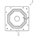
- FIG. 2A is a top view of the yoke 1 before the coil is embedded.
- the yoke 1 is made of a magnetic material such as ferrite.
- the outer shape of the yoke 1 is a substantially square with a side of about 150 mm.
- the yoke 1 is provided with two grooves 11 having a substantially regular octagonal shape and a width of about 5 mm and a depth of about 10 mm.
- channel 11 for embedding a coil should just be formed in the yoke 1, and there is no restriction
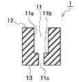
- FIG. 2B is a cross-sectional view taken along the line AA in FIG. 2A.
- the yoke 1 has an upper surface 12 and a lower surface 13 that are parallel to each other. And the groove
- the bottom surface 11 b of the groove 11 has a hole 11 c that reaches the lower surface 13.
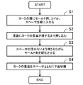
- FIG. 3 is a manufacturing process diagram of a coil-integrated yoke. First, the molding agent 2, the coil 3, and the spacer 4 are put in the groove 11 in order (step S1). As a result, the state shown in FIG. 4 is obtained.
- the molding agent 2 is formed of, for example, a silicon-based material and has flexibility at room temperature but is cured by heating. A part of the molding agent 2 may be pushed into the hole 11c.
- the coil 3 is molded in advance so as to fit into the groove 11.
- the coil 3 hits the yoke 1, and the corner 11 d of the groove 11 may be missing, but this is not a problem in this embodiment.
- the spacer 4 is a plate-like member having a rectangular cross section formed of a non-magnetic material such as aluminum, copper, titanium, plastic or the like.
- the width of the spacer 4 is slightly smaller than the width of the groove 11, and both side surfaces of the spacer 4 abut against both side surfaces 11 a of the groove 11.
- the spacer 4 has the same rigidity as the coil 3, for example, the difference or ratio between them is not more than a predetermined value.
- the yoke 1 is turned upside down as necessary, the flat surface plate 5 and the upper surface 12 of the yoke 1 are pressed against each other (FIG. 5), and the spacer 4 is moved until the upper surface 12 of the yoke 1 contacts the surface plate 5.
- Push in step S2 in FIG. 3.
- the molding agent 2 is deformed and pushed into the hole 11c or enters the coil 3, so that the entire spacer 4 is accommodated in the groove 11 and the state shown in FIG. 6 is obtained. That is, the upper surface 12 of the yoke 1 and the upper surface 41 of the spacer 4 are flush with each other.
- the mold agent 2 is cured by heating while pressing the molding agent 2 and the coil 3 with a pressing member such as a rod 6 using the hole 11c so that the spacer 4 does not float (step S3 in FIG. 3).
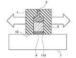
- the upper surface 12 of the yoke 1 is flatly polished together with the spacer 4 by using the polishing disc 7 so that the corner 11d becomes a right angle (step S4, FIG. 7).
- the upper surface 12 of the yoke 1 can be flattened, and since the spacer 4 is present in the groove 11, the corner 11d of the groove 11 is not lost during polishing.
- the angle formed by the upper surface 12 of the yoke 1 and the side surface 11a of the groove 11 a right angle so that there is no chipping of 5 ⁇ m or less, the disturbance of the magnetic field lines can be sufficiently suppressed.
- the distance between the upper surface of the yoke 1 and the coil 3 can be set to a desired constant value.
- the coil-integrated yoke manufactured as described above includes the yoke 1 provided with the groove 11, the molding agent 2, the coil 3, and the spacer 4 arranged (cured) in this order from the bottom surface 11 b side (lower surface 13 side) of the groove 11. It has.
- the upper surface 12 of the yoke 1 and the upper surface of the spacer 4 are flush with each other, and the angle between the upper surface 12 of the yoke 1 and the side surface 11a of the groove 11 is approximately 90 degrees.
- the molding agent 2, the coil 3, and the spacer 4 are put in the groove 11 of the yoke 1, and the upper surface 12 of the yoke 1 is planarly polished together with the spacer 4.
- the upper surface 12 of the yoke 1 and the side surface 11a of the groove 11 become a right angle.
Landscapes
- Engineering & Computer Science (AREA)
- Power Engineering (AREA)
- Physics & Mathematics (AREA)
- Electromagnetism (AREA)
- Manufacturing & Machinery (AREA)
- Chemical & Material Sciences (AREA)
- Analytical Chemistry (AREA)
- Electromagnets (AREA)
Abstract
精度よく電子ビームの軌道を偏向可能な偏向器を実現するためのコイル一体型ヨークおよびその製造方法を提供する。 ヨークの第1面から第2面に向かう溝にモールド剤、コイルおよびスペーサを順に入れる工程と、前記ヨークの第1面を前記スペーサとともに研磨する工程と、を備えるコイル一体型ヨークの製造方法が提供される。
Description
本発明は、コイル一体型ヨークおよびその製造方法に関する。
SEM(Scanning Electron Microscope)など電子ビームを照射する装置において、電子ビームの軌道上に偏向器を設置し、電子ビームの軌道を偏向することが行われている。偏向器として、ヨークに埋め込まれたコイルに通電することで生じる磁場で電子ビームを偏向する磁場偏向器が知られている。
本発明の課題は、精度よく電子ビームの軌道を偏向可能な偏向器を実現するためのコイル一体型ヨークおよびその製造方法を提供することである。
本発明の一態様によれば、ヨークの第1面から第2面に向かう溝にモールド剤、コイルおよびスペーサを順に入れる工程と、前記ヨークの第1面を前記スペーサとともに研磨する工程と、を備えるコイル一体型ヨークの製造方法が提供される。
前記ヨークの第1面と、前記溝の側面とのなす角度が90度となるよう、前記ヨークの第1面を前記スペーサとともに研磨するのが望ましい。
前記スペーサは、前記ヨークと同程度の剛性を有するのが望ましい。
前記溝の底部には、前記第2面に到達する穴があり、前記モールド剤、前記コイルおよび前記スペーサを前記溝に入れる工程の後に、前記穴を利用して前記モールド剤を押さえた状態で前記モールド剤を硬化させる工程を備えるのが望ましい。
前記スペーサを前記溝に入れる工程では、前記スペーサの一部のみが前記溝内に入るようにし、その後、前記スペーサと前記ヨークの第1面とが面一になるようにした状態で、前記ヨークの第1面を前記スペーサとともに研磨するのが望ましい。
本発明の別の態様によれば、第1面および第2面を有し、前記第1面から前記第2面に向かう溝が設けられたヨークと、前記第2面側から順に前記溝内に配置されたモールド剤、コイルおよびスペーサと、を備え、前記ヨークの第1面と、前記スペーサとは面一であり、前記ヨークの第1面と、前記溝の側面とがなす角度が90度である、コイル一体型ヨークが提供される。
精度よく電子ビームの軌道を偏向可能な偏向器を実現できる。
以下、本発明に係る実施形態について、図面を参照しながら具体的に説明する。
図1は、SEMの概略構成図である。SEMは、真空管(不図示)内に配置された電子銃91、偏向器92などを備えている。電子銃91からの電子ビームは偏向器92によって偏向されて、試料Wに到達する。試料Wから反射したミラー電子を捕捉することで、試料Wの表面を観察できる。
偏向器92は平面ヨーク92aの溝(凹部)にコイル92bを埋め込んで構成される。コイル92bに通電することで磁場が発生して電子ビームが偏向される。ここで、ヨーク92aの溝にコイル92bを埋め込む際に、角(図1の破線で囲んだ部分)が欠けることがある。角が直角でない場合、コイル92bからの磁力線が乱れ、理論通りに電子ビームを偏向できないことがある。そこで、本実施形態では次のようにしてコイル92bを埋め込んだヨーク92a(コイル一体型ヨーク)を製造する。
図2Aは、コイルを埋め込む前のヨーク1の上面図である。ヨーク1はフェライトなどの磁性材料で形成される。ヨーク1の外郭は一辺が約150mmの概略正方形である。ヨーク1には、概略正八角形で、幅約5mm、深さ約10mmの2つの溝11が設けられている。なお、ヨーク1にはコイルを埋め込むための溝11が形成されていればよく、大きさや形状に特に制限はない。
図2Bは、図2AのA-A断面図である。ヨーク1は、互いに平行な上面12および下面13を有する。そして、上面12から下面13に向かう溝11が形成されており、上面12と溝11の側面11aとのなす角度はほぼ90度である。なお、この時点では厳密に90度である必要はない。また、溝11の底面11bには穴11cがあり、下面13まで到達している。
図3は、コイル一体型ヨークの製造工程図である。まず、溝11にモールド剤2、コイル3およびスペーサ4を順に入れる(ステップS1)。これにより、図4に示す状態となる。
モールド剤2は、例えばシリコン系の材料で形成され、常温では柔軟性を有するが加熱することによって硬化する。モールド剤2の一部が穴11cに押し込まれてもよい。
コイル3は溝11に嵌まるよう予め成型されている。コイル3を溝11に入れる際、コイル3がヨーク1に当たって、溝11の角11dが欠けることがあるが、本実施形態においては問題とならない。
スペーサ4は非磁性材料、例えばアルミニウム、銅、チタン、プラスティックなどで形成された断面が長方形の板状部材である。スペーサ4の幅は溝11の幅よりわずかに小さい程度であり、スペーサ4の両側面は溝11の両側面11aにそれぞれ当接する。後にコイル3とともにスペーサ4を研磨する都合上、スペーサ4はコイル3と剛性が同程度、例えば両者の差あるいは比が所定値以下であるのが望ましい。また、スペーサ4は、全体ではなく、一部(半分程度)のみが溝11内に入り、残りの一部は上面からはみ出ているのが望ましい。
続いて、必要に応じてヨーク1を上下反転し、平坦な定盤5とヨーク1の上面12とを互いに押し当て(図5)、定盤5にヨーク1の上面12が接するまでスペーサ4を押し込む(図3のステップS2)。これにより、モールド剤2が変形して穴11cに押し出されたりコイル3の内部に入り込んだりして、スペーサ4の全体が溝11内に収まり、図6に示す状態となる。すなわち、ヨーク1の上面12とスペーサ4の上面41とが面一となる。
その後、スペーサ4が浮かないよう、穴11cを利用して棒6などの押さえ部材でモールド剤2およびコイル3を押さえつつ、加熱を行ってモールド剤2を硬化させる(図3のステップS3)。
そして、角11dが直角となるよう、研磨盤7を用いてヨーク1の上面12をスペーサ4とともに平坦研磨する(ステップS4、図7)。研磨によってヨーク1の上面12を平坦化でき、溝11内にスペーサ4が存在するので研磨の際に溝11の角11dが欠けることもない。ヨーク1の上面12と溝11の側面11aとが形成する角を5μm以下の欠けがない程度に直角とすることで、磁力線の乱れを十分に抑制できる。また、スペーサ4を設けることで、ヨーク1の上面とコイル3との距離を所望の一定値とすることもできる。
以上により製造されるコイル一体型ヨークは、溝11が設けられたヨーク1と、溝11の底面11b側(下面13側)から順に配置された(硬化した)モールド剤2、コイル3およびスペーサ4を備えている。そして、ヨーク1の上面12とスペーサ4の上面とは面一であり、ヨーク1の上面12と溝11の側面11aとのなす角度がほぼ90度である。
このように、本実施形態では、ヨーク1の溝11にモールド剤2、コイル3およびスペーサ4を入れて、スペーサ4とともにヨーク1の上面12を平面研磨する。これにより、ヨーク1の上面12と溝11の側面11aとが直角となる。このようなコイル一体型ヨークを偏向器92に適用することで、精度よく電子ビームの軌道を偏向できる。
上述した実施形態は、本発明が属する技術分野における通常の知識を有する者が本発明を実施できることを目的として記載されたものである。上記実施形態の種々の変形例は、当業者であれば当然になしうることであり、本発明の技術的思想は他の実施形態にも適用しうることである。したがって、本発明は、記載された実施形態に限定されることはなく、特許請求の範囲によって定義される技術的思想に従った最も広い範囲とすべきである。
1 ヨーク
11 溝
11a 側面
11b 底面
11c 穴
12 上面
13 下面
2 モールド剤
3 コイル
4 スペーサ
5 定盤
6 棒
7 研磨盤
11 溝
11a 側面
11b 底面
11c 穴
12 上面
13 下面
2 モールド剤
3 コイル
4 スペーサ
5 定盤
6 棒
7 研磨盤
Claims (6)
- ヨークの第1面から第2面に向かう溝にモールド剤、コイルおよびスペーサを順に入れる工程と、
前記ヨークの第1面を前記スペーサとともに研磨する工程と、を備えるコイル一体型ヨークの製造方法。 - 前記ヨークの第1面と、前記溝の側面とのなす角度が90度となるよう、前記ヨークの第1面を前記スペーサとともに研磨する、請求項1に記載のコイル一体型ヨークの製造方法。
- 前記スペーサは、前記ヨークと同程度の剛性を有する、請求項1または2に記載のコイル一体型ヨークの製造方法。
- 前記溝の底部には、前記第2面に到達する穴があり、
前記モールド剤、前記コイルおよび前記スペーサを前記溝に入れる工程の後に、前記穴を利用して前記モールド剤を押さえた状態で前記モールド剤を硬化させる工程を備える、請求項1乃至3のいずれかに記載のコイル一体型ヨークの製造方法。 - 前記スペーサを前記溝に入れる工程では、前記スペーサの一部のみが前記溝内に入るようにし、
その後、前記スペーサと前記ヨークの第1面とが面一になるようにした状態で、前記ヨークの第1面を前記スペーサとともに研磨する、請求項1乃至4のいずれかに記載のコイル一体型ヨークの製造方法。 - 第1面および第2面を有し、前記第1面から前記第2面に向かう溝が設けられたヨークと、
前記第2面側から順に前記溝内に配置されたモールド剤、コイルおよびスペーサと、を備え、
前記ヨークの第1面と、前記スペーサとは面一であり、
前記ヨークの第1面と、前記溝の側面とがなす角度が90度である、コイル一体型ヨーク。
Priority Applications (1)
| Application Number | Priority Date | Filing Date | Title |
|---|---|---|---|
| US16/461,109 US11164697B2 (en) | 2017-04-07 | 2018-04-04 | Coil-integrated-type yoke and manufacturing method of the same |
Applications Claiming Priority (2)
| Application Number | Priority Date | Filing Date | Title |
|---|---|---|---|
| JP2017-076547 | 2017-04-07 | ||
| JP2017076547A JP6895299B2 (ja) | 2017-04-07 | 2017-04-07 | コイル一体型ヨークおよびその製造方法 |
Publications (1)
| Publication Number | Publication Date |
|---|---|
| WO2018186427A1 true WO2018186427A1 (ja) | 2018-10-11 |
Family
ID=63712468
Family Applications (1)
| Application Number | Title | Priority Date | Filing Date |
|---|---|---|---|
| PCT/JP2018/014354 Ceased WO2018186427A1 (ja) | 2017-04-07 | 2018-04-04 | コイル一体型ヨークおよびその製造方法 |
Country Status (3)
| Country | Link |
|---|---|
| US (1) | US11164697B2 (ja) |
| JP (1) | JP6895299B2 (ja) |
| WO (1) | WO2018186427A1 (ja) |
Citations (6)
| Publication number | Priority date | Publication date | Assignee | Title |
|---|---|---|---|---|
| JPH02246302A (ja) * | 1989-03-20 | 1990-10-02 | Tdk Corp | ロータリートランス用コイル装置及びその製造方法 |
| JPH04284608A (ja) * | 1991-03-13 | 1992-10-09 | Sony Chem Corp | 接着剤付きコイル及びロータリートランス |
| JPH05275225A (ja) * | 1992-03-25 | 1993-10-22 | Sony Corp | Mn−Zn系フェライト磁気コア及びその製造方法 |
| JPH06124654A (ja) * | 1992-10-13 | 1994-05-06 | Murata Mfg Co Ltd | コイルの形成方法 |
| JPH11307383A (ja) * | 1998-04-23 | 1999-11-05 | Sony Corp | ロータリートランスの製造方法 |
| JP2016082187A (ja) * | 2014-10-22 | 2016-05-16 | 日本圧着端子製造株式会社 | 電気的接続装置 |
Family Cites Families (6)
| Publication number | Priority date | Publication date | Assignee | Title |
|---|---|---|---|---|
| JPS5554101Y2 (ja) * | 1975-09-03 | 1980-12-15 | ||
| JPS58161312A (ja) | 1982-03-18 | 1983-09-24 | Toshiba Corp | モ−ルドコイルの製造方法 |
| JPS63167276A (ja) * | 1986-12-27 | 1988-07-11 | Jeco Co Ltd | サ−ボ型加速度計 |
| SE9504204L (sv) * | 1995-11-24 | 1997-03-10 | Ericsson Telefon Ab L M | Induktiv komponent samt förfarande för tillverkning av en sådan |
| JP2002191150A (ja) * | 2000-12-19 | 2002-07-05 | Sankyo Seiki Mfg Co Ltd | モータ |
| JP6547239B2 (ja) | 2014-05-14 | 2019-07-24 | Tdk株式会社 | 平面コイルユニット |
-
2017
- 2017-04-07 JP JP2017076547A patent/JP6895299B2/ja active Active
-
2018
- 2018-04-04 US US16/461,109 patent/US11164697B2/en active Active
- 2018-04-04 WO PCT/JP2018/014354 patent/WO2018186427A1/ja not_active Ceased
Patent Citations (6)
| Publication number | Priority date | Publication date | Assignee | Title |
|---|---|---|---|---|
| JPH02246302A (ja) * | 1989-03-20 | 1990-10-02 | Tdk Corp | ロータリートランス用コイル装置及びその製造方法 |
| JPH04284608A (ja) * | 1991-03-13 | 1992-10-09 | Sony Chem Corp | 接着剤付きコイル及びロータリートランス |
| JPH05275225A (ja) * | 1992-03-25 | 1993-10-22 | Sony Corp | Mn−Zn系フェライト磁気コア及びその製造方法 |
| JPH06124654A (ja) * | 1992-10-13 | 1994-05-06 | Murata Mfg Co Ltd | コイルの形成方法 |
| JPH11307383A (ja) * | 1998-04-23 | 1999-11-05 | Sony Corp | ロータリートランスの製造方法 |
| JP2016082187A (ja) * | 2014-10-22 | 2016-05-16 | 日本圧着端子製造株式会社 | 電気的接続装置 |
Also Published As
| Publication number | Publication date |
|---|---|
| JP6895299B2 (ja) | 2021-06-30 |
| US11164697B2 (en) | 2021-11-02 |
| US20200066477A1 (en) | 2020-02-27 |
| JP2018181971A (ja) | 2018-11-15 |
Similar Documents
| Publication | Publication Date | Title |
|---|---|---|
| KR100996157B1 (ko) | Mems 센서 및 제조방법 | |
| US6281508B1 (en) | Precision alignment and assembly of microlenses and microcolumns | |
| WO2018089579A3 (en) | Scandium-containing iii-n etch-stop layers for selective etching of iii-nitrides and related materials | |
| JP6704837B2 (ja) | 保持装置 | |
| JP6266747B2 (ja) | 液密な接点スリーブ | |
| TWI687998B (zh) | 製造半導體結構的方法 | |
| US10683204B2 (en) | Semiconductor arrangement and formation thereof | |
| JP2020527850A (ja) | 流体アセンブリ基体およびその製造方法 | |
| WO2018186427A1 (ja) | コイル一体型ヨークおよびその製造方法 | |
| US20150138656A1 (en) | Chip Substrate Having a Lens Insert | |
| US20100187684A1 (en) | System and Method for 3D Integrated Circuit Stacking | |
| CN108242398A (zh) | 在晶片表面形成复杂曲面的方法 | |
| US10947110B2 (en) | MEMS microphone and manufacturing method for making same | |
| JP6818843B2 (ja) | スーパーストレートおよびその使用方法 | |
| JP2009294081A (ja) | Mems製造方法 | |
| KR101214431B1 (ko) | 마이크로 그리드 게이트 및 이를 포함하는 트라이오드 | |
| KR101739795B1 (ko) | 에지링 및 그의 제조방법 | |
| US20070172968A1 (en) | Method of processing semiconductor substrate | |
| TW517168B (en) | Method to produce a light-coupling-out plane of a light-waveguide | |
| KR100994476B1 (ko) | 정전척 및 그 제조방법 | |
| KR20140145468A (ko) | 자성체를 이용한 플라즈마 식각장치 | |
| JPS63285914A (ja) | 電磁石 | |
| KR20090052350A (ko) | 전자 칼럼용 렌즈 조립체 | |
| KR101048341B1 (ko) | 전자빔용 렌즈 및 이의 제조방법 | |
| KR101386004B1 (ko) | 웨이퍼 접합 기술을 활용한 마이크로 그리드 구조물 제조 방법 |
Legal Events
| Date | Code | Title | Description |
|---|---|---|---|
| 121 | Ep: the epo has been informed by wipo that ep was designated in this application |
Ref document number: 18780395 Country of ref document: EP Kind code of ref document: A1 |
|
| NENP | Non-entry into the national phase |
Ref country code: DE |
|
| 122 | Ep: pct application non-entry in european phase |
Ref document number: 18780395 Country of ref document: EP Kind code of ref document: A1 |