WO2018186302A1 - Élément de capture d'image et dispositif de capture d'image - Google Patents
Élément de capture d'image et dispositif de capture d'image Download PDFInfo
- Publication number
- WO2018186302A1 WO2018186302A1 PCT/JP2018/013712 JP2018013712W WO2018186302A1 WO 2018186302 A1 WO2018186302 A1 WO 2018186302A1 JP 2018013712 W JP2018013712 W JP 2018013712W WO 2018186302 A1 WO2018186302 A1 WO 2018186302A1
- Authority
- WO
- WIPO (PCT)
- Prior art keywords
- pixel
- charge
- signal
- unit
- transfer unit
- Prior art date
Links
Images


Classifications
-
- H—ELECTRICITY
- H04—ELECTRIC COMMUNICATION TECHNIQUE
- H04N—PICTORIAL COMMUNICATION, e.g. TELEVISION
- H04N25/00—Circuitry of solid-state image sensors [SSIS]; Control thereof
- H04N25/70—SSIS architectures; Circuits associated therewith
- H04N25/76—Addressed sensors, e.g. MOS or CMOS sensors
- H04N25/77—Pixel circuitry, e.g. memories, A/D converters, pixel amplifiers, shared circuits or shared components
-
- G—PHYSICS
- G02—OPTICS
- G02B—OPTICAL ELEMENTS, SYSTEMS OR APPARATUS
- G02B7/00—Mountings, adjusting means, or light-tight connections, for optical elements
- G02B7/28—Systems for automatic generation of focusing signals
- G02B7/34—Systems for automatic generation of focusing signals using different areas in a pupil plane
-
- G—PHYSICS
- G03—PHOTOGRAPHY; CINEMATOGRAPHY; ANALOGOUS TECHNIQUES USING WAVES OTHER THAN OPTICAL WAVES; ELECTROGRAPHY; HOLOGRAPHY
- G03B—APPARATUS OR ARRANGEMENTS FOR TAKING PHOTOGRAPHS OR FOR PROJECTING OR VIEWING THEM; APPARATUS OR ARRANGEMENTS EMPLOYING ANALOGOUS TECHNIQUES USING WAVES OTHER THAN OPTICAL WAVES; ACCESSORIES THEREFOR
- G03B13/00—Viewfinders; Focusing aids for cameras; Means for focusing for cameras; Autofocus systems for cameras
- G03B13/32—Means for focusing
- G03B13/34—Power focusing
- G03B13/36—Autofocus systems
-
- H—ELECTRICITY
- H04—ELECTRIC COMMUNICATION TECHNIQUE
- H04N—PICTORIAL COMMUNICATION, e.g. TELEVISION
- H04N23/00—Cameras or camera modules comprising electronic image sensors; Control thereof
- H04N23/60—Control of cameras or camera modules
- H04N23/667—Camera operation mode switching, e.g. between still and video, sport and normal or high- and low-resolution modes
-
- H—ELECTRICITY
- H04—ELECTRIC COMMUNICATION TECHNIQUE
- H04N—PICTORIAL COMMUNICATION, e.g. TELEVISION
- H04N23/00—Cameras or camera modules comprising electronic image sensors; Control thereof
- H04N23/60—Control of cameras or camera modules
- H04N23/67—Focus control based on electronic image sensor signals
- H04N23/672—Focus control based on electronic image sensor signals based on the phase difference signals
-
- H—ELECTRICITY
- H04—ELECTRIC COMMUNICATION TECHNIQUE
- H04N—PICTORIAL COMMUNICATION, e.g. TELEVISION
- H04N23/00—Cameras or camera modules comprising electronic image sensors; Control thereof
- H04N23/70—Circuitry for compensating brightness variation in the scene
- H04N23/75—Circuitry for compensating brightness variation in the scene by influencing optical camera components
-
- H—ELECTRICITY
- H04—ELECTRIC COMMUNICATION TECHNIQUE
- H04N—PICTORIAL COMMUNICATION, e.g. TELEVISION
- H04N25/00—Circuitry of solid-state image sensors [SSIS]; Control thereof
- H04N25/70—SSIS architectures; Circuits associated therewith
- H04N25/703—SSIS architectures incorporating pixels for producing signals other than image signals
- H04N25/704—Pixels specially adapted for focusing, e.g. phase difference pixel sets
Definitions
- the present invention relates to an imaging element and an imaging apparatus.
- An imaging element that reads signals from a plurality of photoelectric conversion units from a pixel having a plurality of photoelectric conversion units and a plurality of floating diffusion units is known (see Patent Document 1).
- the plurality of photoelectric conversion units are connected to the plurality of floating diffusion units, respectively.
- the imaging device photoelectrically converts light transmitted through the microlens to generate a first charge, and photoelectrically converts light transmitted through the microlens.
- a second photoelectric conversion unit that generates a second charge; a storage unit that stores at least one of the first charge and the second charge; a first transfer unit that transfers the first charge to the storage unit; A first transfer unit that includes a second transfer unit that transfers the second charge to the storage unit; and the first charge of the first pixel and the second charge of the second pixel.
- an imaging device includes an imaging element according to the first aspect and the first pixel and the second pixel of the imaging element that capture an image by an optical system having a focus adjustment optical system.
- a position control unit that controls the position of the focus adjustment optical system so that an image by the optical system is focused on the image sensor based on the output signal based on the first charge and the signal based on the second charge. And comprising.
- the imaging apparatus outputs the image of the first pixel output from the imaging element that captures an image by the optical system having the imaging element according to the first aspect and a focus adjustment optical system. At least one of a signal based on the first charge and a signal based on the second charge of the second pixel, and a signal based on the second charge of the first pixel and a signal based on the first charge of the second pixel And a position control unit that controls the position of the focus adjustment optical system so that an image formed by the optical system is focused on the image sensor.
- FIG. 4 is a circuit diagram illustrating pixels arranged in an M column in FIG. 3.
- FIG. 4 is a circuit diagram illustrating pixels arranged in an M + 1 column in FIG. 3.
- FIG. 8 is a circuit diagram illustrating pixels arranged in an M column in FIG. 7.
- FIG. 9A to FIG. 9D are diagrams illustrating a series and b series signals according to the second embodiment.
- FIG. 11 is a circuit diagram illustrating pixels arranged in an M column in FIG. 10.
- FIGS. 12A and 12B are diagrams exemplifying a-sequence and b-sequence signals in the third embodiment. It is a figure which illustrates pixel arrangement in modification 1 of a 3rd embodiment.
- FIG. 14A to FIG. 14C are diagrams illustrating a series and b series signals according to the fourth embodiment. It is a flowchart explaining the flow of the process which a microprocessor performs. It is a flowchart explaining the flow of the process which a microprocessor performs. It is a flowchart explaining the flow of the process which a microprocessor performs. It is a flowchart explaining the flow of the process which a microprocessor performs. It is a figure which illustrates pixel arrangement
- FIG. 1 is a block diagram illustrating a digital camera 1 (hereinafter referred to as camera 1) equipped with a focus detection device using a solid-state image sensor 3 (hereinafter referred to as image sensor 3) according to the first embodiment.
- the lens interchangeable camera 1 such as a single lens reflex type or a mirrorless type will be described as an example.
- the camera may not be a lens interchangeable camera.
- you may comprise as an imaging device like the camera mounted in portable terminals, such as a lens integrated camera or a smart phone.
- the present invention is not limited to still images, and may be configured as an imaging device such as a video camera or mobile camera that captures moving images.
- the camera 1 is equipped with a photographing lens 2 as an imaging optical system.
- the taking lens 2 has a focusing lens and a stop.
- the focusing lens and the aperture of the photographing lens 2 are controlled by the lens control unit 2a that receives an instruction from the microprocessor 9.
- the taking lens 2 forms an optical image (subject image) on the image pickup surface of the image pickup device 3.
- the taking lens 2 is also referred to as an imaging optical system.
- the image sensor 3 has a plurality of pixels. As will be described later, each of the plurality of pixels has two photoelectric conversion units that generate charges by photoelectrically converting incident light. The plurality of pixels photoelectrically convert the light transmitted through the photographing lens 2. The plurality of pixels each output a signal based on the charge generated by the photoelectric conversion.
- the imaging element 3 is controlled by the imaging control unit 4 that receives an instruction from the microprocessor 9. Signals output from a plurality of pixels included in the image sensor 3 are processed through the signal processing unit 5 and the A / D conversion unit 6 and then temporarily stored in the memory 7.
- the imaging device 3 may include a part or all of the signal processing unit 5, the A / D conversion unit 6, and the memory 7.
- the imaging device 3 may have a configuration in which at least one of the signal processing unit 5, the A / D conversion unit 6, and the memory 7 and a plurality of pixels are stacked.
- the microprocessor 9 receives an operation signal from an operation unit 9a such as a release button.
- the microprocessor 9 controls the camera 1 by sending an instruction to each block based on the operation signal from the operation unit 9a.
- the focus calculation unit 10 calculates a focus adjustment state by the photographing lens 2 by a pupil division type phase difference detection method based on a signal from a pixel included in the image sensor 3.
- the focus calculation unit 10 captures an image from the imaging lens 2 by the imaging element 3 based on signals based on charges generated by first and second photodiodes PD-1 and PD-2 included in a pixel 20 described later.
- the focus position of the focus lens for focusing on the surface is calculated. Specifically, an image shift amount of a plurality of light beams that have passed through different areas of the pupil of the photographing lens 2 is detected, and a defocus amount is calculated based on the detected image shift amount.
- the defocus amount is an amount of deviation between the imaging surface on which the image by the photographing lens 2 is formed and the imaging surface of the image sensor 3. Since the calculation of the defocus amount by the phase difference detection method is known, a detailed description thereof is omitted.
- the focus calculation unit 10 calculates the amount of movement of the focus lens to the in-focus position based on the calculated defocus amount.
- the microprocessor 9 instructs the lens control unit 2a to move the focusing lens and sends the calculated movement amount of the focus lens. Thereby, focus adjustment is performed automatically.
- the focus calculation unit 10, the microprocessor 9, and the lens control unit 2a operate as a focus adjustment unit.
- the image processing unit 13 performs predetermined image processing on the signal from the image sensor 3 stored in the memory 7 to generate image data.
- the image processing unit 13 operates as an image generation unit.
- the image compression unit 12 compresses the image data after image processing in a predetermined format.
- the recording unit 11 records the compressed image data on the recording medium 11a in a predetermined file format, and reads the image data recorded on the recording medium 11a.
- the recording medium 11 a is configured by a memory card that is detachable from the recording unit 11.
- the image processing unit 13 generates image data for causing the display unit 14 to display an image.
- the display unit 14 displays an image based on the image data generated by the image processing unit 13.
- the images displayed by the display unit 14 include reproduced images (still images, moving images) based on image data recorded in the recording medium 11a, and monitor images acquired at a predetermined interval (for example, 60 fps) by the image sensor 3. (Also referred to as a live view image).
- FIG. 2 is a diagram illustrating a schematic configuration of the image sensor 3.
- the imaging device 3 includes a plurality of pixels 20 arranged in a matrix and a peripheral circuit for outputting a signal from each pixel 20.
- a minimum unit that constitutes an image is referred to as a “pixel”.
- a configuration that generates a signal of the minimum unit that constitutes an image is referred to as a “pixel”.
- the imaging area 31 is an area where the pixels 20 are arranged in a matrix. In the example of FIG. 2, a range of 16 pixels of 4 rows horizontally and 4 columns vertically is illustrated as the imaging region 31, but the actual number of pixels is much larger than that illustrated in FIG. 2.
- FIG. 3 is a diagram illustrating the pixel arrangement of the image sensor 3.
- the pixel 20 is provided with a microlens ML and a color filter (not shown).
- the color filter is provided with one of three color filters having different spectral characteristics of, for example, R (red), G (green), and B (blue) for each pixel 20.
- the R color filter mainly transmits light in the red wavelength region.
- the G color filter mainly transmits light in the green wavelength region.
- the B color filter mainly transmits light in a blue wavelength region.
- the G color filter transmits light in a wavelength region having a shorter wavelength than the R color filter.
- the B color filter transmits light having a shorter wavelength than the G color filter.
- each pixel 20 has different spectral characteristics depending on the arranged color filter.
- the image sensor 3 includes a pixel row in which pixels 20 having R and G color filters (hereinafter referred to as pixels 20R and 20G, respectively) are alternately arranged, and a pixel 20 having G and B color filters (hereinafter referred to as pixels 20R and 20G). Pixel rows in which the pixels 20G and the pixels 20B are alternately arranged) are repeatedly arranged in a two-dimensional manner.
- the pixel 20R, the pixel 20G, and the pixel 20B are arranged according to the Bayer array.
- the pixel 20 is referred to without R, G, and B
- the pixel 20R, the pixel 20G, and the pixel 20B are all included.
- Each pixel 20 is provided with two photoelectric conversion units.
- two photoelectric conversion units are provided per pixel
- two photoelectric conversion units are arranged in the horizontal direction, that is, in the row direction (also referred to as horizontal division)
- two photoelectric conversion units are in the vertical direction, that is, There are cases where they are arranged in the column direction (also referred to as vertical division).
- the horizontally divided pixels 20 are arranged over the entire imaging region 31.
- the vertically divided pixels 20 may be arranged in the predetermined area instead of the horizontally divided pixels 20.
- Each pixel 20 performs photoelectric conversion by two photoelectric conversion units in accordance with a control signal from a peripheral circuit, and outputs a signal based on the charge generated by the photoelectric conversion unit.
- the peripheral circuit includes, for example, a vertical scanning circuit 21, a horizontal scanning circuit 22, control signal lines 23 and 24 connected thereto, a vertical signal line 25 that receives a signal from the pixel 20, and a vertical signal line 25.
- CDS circuit correlated double sampling circuit
- one vertical signal line 25 is provided for one pixel column composed of a plurality of pixels 20 arranged in the column direction.
- the vertical scanning circuit 21 and the horizontal scanning circuit 22 are configured by a first control signal ⁇ Tx1, a second control signal ⁇ Tx2, a control signal ⁇ SEL, and a control signal ⁇ RES, which will be described later, via a control signal line 23 in response to an instruction from the imaging control unit 4. Is output to the pixel 20.
- Each pixel 20 is driven by a control signal output from the vertical scanning circuit 21 and outputs a signal based on the charge generated by the photoelectric conversion unit to the vertical signal line 25.
- the signal output from the pixel 20 is subjected to noise removal by the CDS circuit 27, and is output to the outside through the horizontal signal line 28 and the output amplifier 29 by the control signal from the horizontal scanning circuit 22.
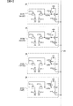
- FIG. 4 shows pixels 20 arranged in M columns (vertically arranged) in FIG. 3, that is, for example, a pixel 20G in the Nth row, a pixel 20R in the N + 1th row, a pixel 20G in the N + 2th row, and a N + 3th row. It is a circuit diagram explaining the pixel 20R.
- Each pixel 20 has two photodiodes PD-1 and PD-2 as photoelectric conversion units inside a microlens and a color filter (not shown).
- each pixel 20 includes a first photodiode PD-1 disposed on the left side of the pixel 20 and a second photodiode PD-2 disposed on the right side of the pixel 20. Therefore, the light beam that has passed through the first region of the pupil of the photographic lens 2 is incident on the first photodiode PD-1 of each pixel 20, and the second photodiode PD-2 is incident on the photographic lens 2. The light beam that has passed through the second region of the pupil enters.
- signals based on the charges generated by the first photodiode PD-1 and the second photodiode PD-2 and the first and second photodiodes PD-1 and PD-2 are referred to as “pixel”.
- the reading unit includes a transfer transistor, an FD region, an amplification transistor, and a selection transistor, which will be described later, will be described.
- the range of the reading unit is not necessarily the same as this example.
- the first and second photodiodes PD-1 and PD-2 have light passing through different regions of the pupil of the photographing lens 2, that is, the first and second regions, respectively. Is incident.
- the first and second photodiodes PD-1 and PD-2 generate charges by photoelectrically converting incident light, respectively. Charges generated by the first photodiode PD-1 and the second photodiode PD-2 are transferred to the common FD (floating diffusion) via the first transfer transistor Tx-1 or the second transfer transistor Tx-2. ) Transferred to the area.
- the common FD area accumulates the received charge and converts it into voltage.
- a signal corresponding to the potential of the FD region is amplified by the amplification transistor AMP.
- the FD region and the amplification transistor AMP operate as a signal generation unit. Then, the generated signal is read out through the vertical signal line 25 (output unit) as a signal of the row selected by the selection transistor SEL that selects the row.
- the reset transistor RES operates as a reset unit that resets the potential of the FD region.
- the charge generated by the first photodiode PD-1 (referred to as the first charge) and the charge generated by the second photodiode PD-2 (the second charge) are transferred to one FD area in a time division manner. That is, the transfer of the charge generated by the first photodiode PD-1 and the transfer of the charge generated by the second photodiode PD-2 use one FD region. For this reason, the on / off state of the first transfer transistor Tx-1 and the second transfer transistor Tx-2 depends on the vertical scanning when the first charge is transferred to the FD region and when the second charge is transferred. Switching is performed by a control signal from the circuit 21.
- a signal based on the first charge generated by the first photodiode PD-1 (referred to as a first signal) and a signal generated by the second photodiode PD-2.
- the signals based on the second charges (referred to as second signals) are sequentially read out in a time division manner via one vertical signal line 25. That is, the common vertical signal line 25 is used for reading the first signal and reading the second signal. Therefore, the ON / OFF states of the first transfer transistor Tx-1 and the second transfer transistor Tx-2 are controlled by the vertical scanning circuit 21 in the case of reading the first signal and the case of reading the second signal. It is switched by a signal.
- a pixel 20 called type P and a pixel 20 called type S are provided.
- the first transfer transistor Tx-1 that transfers the first charge generated by the first photodiode PD-1 to the FD region is turned on by the first control signal ⁇ Tx1.
- the second transfer transistor Tx-2 that transfers the second charge generated by the second photodiode PD-2 to the FD region is turned on by the second control signal ⁇ Tx2.
- the selection transistor SEL for row selection for outputting the first signal or the second signal to the vertical signal line 25 (output unit) is turned on by the control signal ⁇ SEL.
- the reset transistor RES that resets the potential of the FD region is turned on by the control signal ⁇ RES.
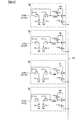
- FIG. 5 shows pixels 20 arranged in the M + 2 column (vertically arranged) in FIG. 3, that is, for example, a pixel 20G in the Nth row, a pixel 20R in the N + 1th row, a pixel 20G in the N + 2th row, and a N + 3th row. It is a circuit diagram explaining the pixel 20R.
- Each pixel 20 includes first and second photodiodes PD-1 and PD-2 as photoelectric conversion portions inside microlenses and color filters (not shown). As described above, the pixel 20 has a horizontal division and a vertical division.
- the light beam that has passed through the first region of the pupil of the photographing lens 2 is incident on the first photodiode PD-1 of each pixel 20, and the second photodiode PD-2 is incident on the photographing lens 2 of the photographing lens 2.
- the point where the light beam that has passed through the second region of the pupil is incident is the same as in the case of FIG.
- Type S The difference between Type S and Type P is that the relationship between the first and second transfer transistors Tx-1, Tx-2 and the first and second control signals ⁇ Tx1, ⁇ Tx2 supplied to them is reversed. Is a point. That is, in type S, the second control signal ⁇ Tx2 is supplied to the first transfer transistor Tx-1, and the first control signal ⁇ Tx1 is supplied to the second transfer transistor Tx-2.
- the first transfer transistor Tx-1 that transfers the first charge generated by the first photodiode PD-1 to the FD region is turned on by the second control signal ⁇ Tx2.
- the second transfer transistor Tx-2 that transfers the second charge generated by the second photodiode PD-2 to the FD region is turned on by the first control signal ⁇ Tx1.
- the selection transistor SEL for row selection for outputting the first signal or the second signal to the vertical signal line 25 (output unit) is turned on by the control signal ⁇ SEL.
- the reset transistor RES that resets the potential of the FD region is turned on by the control signal ⁇ RES.
- ⁇ Pixel arrangement of type P and type S The pixel arrangement of type P and type S will be described. Focusing on the 2 ⁇ 2 pixels that are the repeating unit of the Bayer array in FIG. 3, all four pixels of the repeating unit are from type P pixels 20G (P), 20B (P), 20R (P), and 20G (P). And all four pixels of the repeating unit are divided into groups consisting of type S pixels 20G (S), 20B (S), 20R (S), and 20G (S). Among these, all four pixels of the repeating unit are indicated by a group of pixels P of type P 20G (P), 20B (P), 20R (P), 20G (P) surrounded by a thick solid line. Are grouped by type S pixels 20G (S), 20B (S), 20R (S), and 20G (S).
- groups surrounded by thick solid lines and groups surrounded by thick broken lines are alternately arranged in the row direction (horizontal direction).
- the group surrounded by the thick solid line and the group surrounded by the thick broken line are successively arranged in the column direction (vertical direction).
- each pixel 20 in FIG. 3 one of the first and second photodiodes PD-1 and PD-2 is hatched.
- the hatched photodiode indicates a photodiode in which charges generated by the photodiode are transferred to the FD region when the first control signal ⁇ Tx1 is supplied.
- a photodiode that is not hatched indicates a photodiode in which charges generated by the photodiode are transferred to the FD region when the second control signal ⁇ Tx2 is supplied. Therefore, in the type P pixel 20G (P), the first photodiode PD-1 is hatched and the second photodiode PD-2 is not hatched. Conversely, in the type S pixel 20G (S), The second photodiode PD-2 is hatched, and the first photodiode PD-1 is not hatched.
- the type P pixel 20G (P) when the first control signal ⁇ Tx1 is supplied to the first transfer transistor Tx-1, the first charge generated by the first photodiode PD-1 is generated. Are transferred to the FD area. The first signal is generated based on the first charge transferred to the FD region.
- the second control signal ⁇ Tx2 when the second control signal ⁇ Tx2 is supplied to the second transfer transistor Tx-2, the second charge generated by the second photodiode PD-2 is transferred to the FD region. Transferred. The second signal is generated based on the second charge transferred to the FD region.
- the pixel 20G (S) when the first control signal ⁇ Tx1 is supplied to the second transfer transistor Tx-2, the pixel 20G (S) is generated by the second photodiode PD-2 of the pixel 20G (S). The second charge is transferred to the FD region. The second signal is generated based on the second charge transferred to the FD region.
- the first photodiode PD-1 of the pixel 20G (S) when the second control signal ⁇ Tx2 is supplied to the first transfer transistor Tx-1, the first photodiode PD-1 of the pixel 20G (S) generates the first control signal ⁇ Tx2. One charge is transferred to the FD region. The first signal is generated based on the first charge transferred to the FD region.
- the pixels 20 are divided into a group surrounded by a thick solid line and a group surrounded by a thick broken line, and the groups are alternately arranged in the row direction (horizontal direction), and in the column direction (vertical). Each group was arranged side by side.
- the vertical scanning circuit 21 outputs the first control signal ⁇ Tx1, paying attention to the second control signal ⁇ Tx2 and the pixels 20 of the same color arranged in the horizontal direction in the same pixel row, in any pixel row, The first signal and the second signal based on the light passing through different areas of the pupil of the photographing lens 2 are read out simultaneously. For example, attention is paid to the pixels 20G arranged in the horizontal direction in N rows.
- the vertical scanning circuit 21 outputs the first control signal ⁇ Tx1
- the first charge is transferred to the FD region and a first signal is generated.
- the second charge is transferred to the FD region and a second signal is generated.
- the first signal generated by the pixel 20G (P) of N rows and M columns and the second signal generated by the pixel 20G (S) of N rows and M + 2 columns are output to the vertical signal line 25, respectively.
- the vertical scanning circuit 21 outputs the second control signal ⁇ Tx2
- the pixel 20G (P) in the M column the second charge is transferred to the FD region and a second signal is generated.
- the first charge is transferred to the FD region and a first signal is generated.
- the second signal generated by the pixel 20G (P) of N rows and M columns and the first signal generated by the pixel 20G (S) of N rows and M + 2 columns are output to the vertical signal line 25, respectively.
- the imaging device 3 includes the column from which the first signal is read (M column, M + 1 column, M + 4 column, etc. in FIG. 3), The second signal is divided into columns (M + 2 column, M + 3 column, etc. in FIG. 3).
- the camera 1 of the present embodiment uses a first signal and a first signal of the pixel 20G read from a pixel row included in the focus area, for example, as a pair of focus detection signals used for focus detection (in-focus position detection). It generates based on two signals.
- the focus area is an area where the focus calculation unit 10 detects an image shift amount as phase difference information, and is also referred to as a focus detection area, a distance measuring point, or an autofocus (AF) point.
- the microprocessor 9 instructs the imaging control unit 4 to perform imaging for focus adjustment.
- the first readout control signal is supplied from the vertical scanning circuit 21 and the horizontal scanning circuit 22 to the pixel row that is the readout target of the imaging device 3 to perform the first readout.
- the first signal based on the first charge generated by the first photodiode PD-1 from the type P pixel 20G by supplying the first control signal ⁇ Tx1 or the like to each pixel 20G in the pixel row.
- reading a second signal based on the second charge generated by the second photodiode PD-2 from the type S pixel 20G.
- the first signal and the second signal read from each pixel 20G of the pixel row to which the first control signal ⁇ Tx1 is supplied are stored in the memory 7.
- a plurality of first signals A1, A2,..., An (referred to as a series signals) stored in the memory 7, and a plurality of second signals B1, B2,. (Referred to as a signal) represents an intensity distribution of an image by a plurality of light beams that have passed through different areas of the pupil of the photographing lens 2.
- an a-sequence signal and a b-sequence signal can be obtained by performing readout once for each pixel row, 2 pixels for the pixel row are obtained in order to obtain an a-sequence signal and a b-sequence signal from the pixel row. Compared to the case where reading is required once, it is possible to proceed to the image shift detection calculation process earlier. For this reason, the focus adjustment can be performed more quickly.
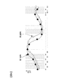
- FIG. 6 is a diagram illustrating an a-sequence signal including a plurality of first signals and a b-sequence signal including a plurality of second signals.
- n a-sequence signals are represented by hatched circles.
- n b-sequence signals are represented by white circles.
- the a-sequence signal and the b-sequence signal from the pixel 20G are read out every three columns in FIG. 3, and the position of the a-sequence signal and the position of the b-sequence signal are equivalent to the two columns in FIG. Has a gap.
- a vertical broken line in FIG. 6 corresponds to a pixel column.
- the focus calculation unit 10 calculates image shift amounts of a plurality of images by performing image shift detection calculation processing (correlation calculation processing, phase difference detection processing) based on the a-sequence signal and the b-sequence signal,
- the defocus amount is calculated by multiplying the image shift amount by a predetermined conversion coefficient.
- the microprocessor 9 determines whether or not the defocus amount calculated by the focus calculation unit 10 is within an allowable value. When the defocus amount exceeds the allowable value, the microprocessor 9 determines that the in-focus state has not been achieved and sends a lens drive instruction to the lens control unit 2a. The lens control unit 2a moves the focusing lens to a position (focus position) where the defocus amount is within an allowable value. On the other hand, if the defocus amount is within the allowable value, the microprocessor 9 determines that the in-focus state is achieved and does not send a lens drive instruction.
- the imaging control unit 4 causes the imaging device 3 to perform the first readout as imaging for focus adjustment.
- the second readout is performed instead of the first readout.
- the second signal based on the second charge generated by the second photodiode PD-2 from the type P pixel 20G by supplying the second control signal ⁇ Tx2 or the like to each pixel 20G in the pixel row.
- a first signal based on the first charge generated by the first photodiode PD-1 from the type S pixel 20G.
- the focus calculation unit 10 performs image shift detection calculation processing (correlation calculation processing, phase difference detection) based on the a-sequence signal stored in the memory 7 by the second reading and the b-sequence signal stored in the memory 7.
- the amount of image shift of a plurality of images is calculated by applying (processing), and the amount of defocus is calculated by multiplying the amount of image shift by a predetermined conversion coefficient.
- the imaging control unit 4 When performing focus adjustment while displaying the monitor image on the display unit 14, the imaging control unit 4 performs the first readout for focus adjustment and the second readout for image on the imaging device 3. It can be done alternately.
- the first readout for focus adjustment and the second readout for image are performed by thinning out the pixels 20 in the imaging region 31 (FIG. 2).
- the microprocessor 9 starts image shift detection calculation processing based on the a-sequence signal and the b-sequence signal stored in the memory 7 by the first reading.
- the microprocessor 9 instructs the imaging control unit 4 to perform the second reading in parallel with the image shift detection calculation process. For example, when the imaging control unit 4 performs the second reading without resetting the potential of the FD region after the first reading, the charge by the second reading is added to the charge by the second reading in the FD region. . Therefore, in the second reading, the sum of the first signal and the second signal is read from each pixel 20 as an image signal.
- the image processing unit 13 generates image data for displaying a monitor image on the display unit 14 by performing predetermined image processing on the sum (image signal) of the first signal and the second signal. .
- the imaging control unit 4 resets the potential of the FD region after the second readout, and repeats the first readout and the second readout again. Thereby, the camera 1 can display the monitor image while adjusting the focus.
- image data used for focus adjustment is generated based on the first signal and the second signal of the pixel 20G read from the pixel row included in the focus area.
- the image data used for focus adjustment is not limited to the first signal and the second signal from the pixel 20G, but may be generated based on the first signal and the second signal from the pixel 20R. It may be generated based on the second signal.
- the camera 1 generates image data related to the subject image based on the first signal and the second signal read from each pixel 20 in the imaging region 31 (FIG. 2). For example, when an operation signal indicating that the release button has been fully pressed is input from the operation unit 9a, the microprocessor 9 instructs the imaging control unit 4 to perform recording imaging. In recording imaging, a control signal is supplied from the vertical scanning circuit 21 and the horizontal scanning circuit 22 to each pixel row of the imaging device 3 to perform first reading and second reading without pixel thinning.
- the imaging control unit 4 supplies the first control signal ⁇ Tx1 and the like to each pixel 20 in the pixel row by the first reading.
- the first control signal ⁇ Tx1 By the supply of the first control signal ⁇ Tx1, the first charge generated by the first photodiode PD-1 of the type P pixel 20 is accumulated in the FD region.
- the second charge of the type S pixel 20 is Second charge generated by the photodiode PD-2 is accumulated in the FD region.
- the imaging control unit 4 performs the second readout without resetting the potential of the FD region after the first readout, and supplies the second control signal ⁇ Tx2 and the like to each pixel 20 in the pixel row.
- the second control signal ⁇ Tx2 By the supply of the second control signal ⁇ Tx2, the second charge generated by the second photodiode PD-2 of the type P pixel 20 is additionally accumulated, that is, added and accumulated in the FD region. Similarly, the first charge generated by the first photodiode PD-1 of the type S pixel 20 is additionally accumulated, that is, added and accumulated in the FD region.
- the first reading and the second reading do not need to be performed at different timings, and the first reading and the second reading may be performed simultaneously. That is, the vertical scanning circuit 21 may supply the first control signal ⁇ Tx1 and the second control signal ⁇ Tx2 to the first transfer transistor Tx-1 and the second transfer transistor Tx-2 simultaneously. .
- an image signal obtained by adding the first signal and the second signal is read out from each pixel 20, and the image processing unit 13 performs gradation processing, color interpolation processing, and the like on the image signal.
- the image data relating to the subject image is generated.
- Image data can be generated as follows instead of the above-described processing. That is, the imaging control unit 4 supplies the first control signal ⁇ Tx1 and the like to each pixel 20 of the pixel row by the first reading to read the first signal from the type P pixel 20, and from the type S pixel 20 Read the second signal. In addition, the imaging control unit 4 performs the second reading after resetting the potential of the FD region after the first reading, and supplies the second control signal ⁇ Tx2 and the like to each pixel 20 in the pixel row to perform the type P pixel. The second signal is read from 20 and the first signal is read from the type S pixel 20.
- the image processing unit 13 adds the first signal and the second signal stored in the memory 7 for each pixel 20 to generate an image signal, and further performs gradation processing, color interpolation processing, etc.
- the image data for is generated.
- the imaging device 3 photoelectrically converts the light transmitted through the microlens ML to generate a first charge, and photoelectrically converts the light transmitted through the microlens ML to the second.
- a second photodiode PD-2 for generating electric charge, an FD region for accumulating at least one of the first electric charge and the second electric charge, and a first transfer transistor Tx-1 for transferring the first electric charge to the FD region;
- the pixel 20G (P), the pixel 20G (S), the first charge of the pixel 20G (P), and the pixel 20G (S) each having a second transfer transistor Tx-2 for transferring the second charge to the FD region.
- the image shift detection calculation process is performed earlier. You can go forward. For this reason, focus adjustment can be performed quickly.
- the vertical scanning circuit 21 transfers the first charge of the pixel 20G (P) to the FD region, and transfers the second charge of the pixel 20G (S) to the FD region. Since the signal ⁇ Tx1 is output to the first transfer transistor Tx-1 of the pixel 20G (P) and the second transfer transistor Tx-2 of the pixel 20G (S), the first control signal ⁇ Tx1 is output to the pixel row.
- An a-sequence signal and a b-sequence signal can be obtained by performing only one reading to supply.
- the vertical scanning circuit 21 includes the vertical scanning circuit 21, the first transfer transistor Tx-1 of the pixel 20G (P), and the second transfer transistor Tx-2 of the pixel 20G (S).
- the first control signal ⁇ Tx1 is output to the first transfer transistor Tx-1 of the pixel 20G (P) and the second transfer transistor Tx-2 of the pixel 20G (S) via the connected control signal line 23. Therefore, an a-sequence signal and a b-sequence signal can be obtained by performing only one readout for supplying the first control signal ⁇ Tx1 to the pixel row.
- the vertical scanning circuit 21 receives the second control signal ⁇ Tx2 for transferring the second charge of the pixel 20G (P) and the first charge of the pixel 20G (S) to the FD region. Since (P) is output to the second transfer transistor Tx-2 and the first transfer transistor Tx-1 of the pixel 20G (S), the second control signal ⁇ Tx2 is supplied to the pixel row once. An a-sequence signal and a b-sequence signal can be obtained simply by reading.
- the vertical scanning circuit 21 transfers the second charge of the pixel 20G (P) to the FD region and transfers the first charge of the pixel 20G (S) to the FD region. Since the signal ⁇ Tx2 is output to the second transfer transistor Tx-2 of the pixel 20G (P) and the first transfer transistor Tx-1 of the pixel 20G (S), the second control signal ⁇ Tx2 is output to the pixel row.
- An a-sequence signal and a b-sequence signal can be obtained by performing only one reading to supply.
- the vertical scanning circuit 21 includes the vertical scanning circuit 21, the second transfer transistor Tx-2 of the pixel 20G (P), and the first transfer transistor Tx-1 of the pixel 20G (S).
- the second control signal ⁇ Tx2 is output to the second transfer transistor Tx-2 of the pixel 20G (P) and the first transfer transistor Tx-1 of the pixel 20G (S) via the connected control signal line 23. Therefore, an a-sequence signal and a b-sequence signal can be obtained by performing only one readout for supplying the second control signal ⁇ Tx2 to the pixel row.
- the pixel 20G (P) and the pixel 20G (S) are arranged, for example, in the row direction (horizontal direction), and the first photodiode PD-1 and the second photodiode PD-2. Are arranged side by side in the row direction (horizontal direction).
- pixel arrangements of type P and type S are different from those in the first embodiment.
- the configurations of the pixel 20 called type P and the pixel 20 called type S are the same as those in the first embodiment.
- the camera 1 in the second embodiment may or may not be an interchangeable lens, as in the first embodiment.
- you may comprise as imaging devices, such as a smart phone and a video camera.
- FIG. 7 is a diagram illustrating a pixel arrangement of the image sensor 3 in the second embodiment.
- all four pixels of the repeating unit are type P pixels 20G (P), 20B (P), 20R (P), 20G (P).
- Group enclosed by a thick solid line
- the microlens ML is not shown.
- the point that the group surrounded by the thick solid line and the group surrounded by the thick broken line are alternately arranged in the row direction (horizontal direction) is also common to the first embodiment.
- this embodiment is different from the first embodiment in that a group surrounded by a thick solid line and a group surrounded by a thick broken line alternately exist in the column direction (vertical direction).
- a group surrounded by a thick solid line and a group surrounded by a thick broken line constitute a so-called checkered pattern.
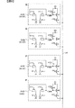
- FIG. 8 shows pixels 20 arranged in the M columns (vertically arranged) in FIG. 7, that is, for example, a pixel 20G (P) in the Nth row, a pixel 20R (P) in the N + 1th row, and a pixel in the N + 2th row. It is a circuit diagram explaining 20G (S) and the pixel 20R (S) of the N + 3 line.
- the point that each pixel 20 has first and second photodiodes PD-1 and PD-2 as photoelectric conversion units inside a microlens and a color filter (not shown) is the same as in the first embodiment.
- the type of the pixels 20 arranged in the vertical direction in FIG. 7 is different from that of the first embodiment in that the type is different every two pixels (type P and type S are repeated).
- each pixel 20 in FIG. 7 one of the first and second photodiodes PD-1 and PD-2 is hatched.
- the hatched photodiode indicates a photodiode in which charges generated by the photodiode are transferred to the FD region when the first control signal ⁇ Tx1 is supplied.
- a photodiode that is not hatched indicates a photodiode in which charges generated by the photodiode are transferred to the FD region when the second control signal ⁇ Tx2 is supplied.
- the type P pixel 20G (P) when the first control signal ⁇ Tx1 is supplied to the first transfer transistor Tx-1, the first charge generated by the first photodiode PD-1 is reduced. Transferred to the FD area.
- the first signal is read based on the first charge transferred to the FD area.
- the second control signal ⁇ Tx2 is supplied to the second transfer transistor Tx-2, the second charge generated by the second photodiode PD-2 is transferred to the FD region. Transferred.
- the second signal is generated based on the second charge transferred to the FD region.
- the type S pixel 20G (S) when the first control signal ⁇ Tx1 is supplied to the second transfer transistor Tx-2, it is generated by the second photodiode PD-2 of the pixel 20G (S). The second charge thus transferred is transferred to the FD region. It shows that the second signal is read based on the second charge transferred to the FD area.
- the type S pixel 20G (S) when the second control signal ⁇ Tx2 is supplied to the first transfer transistor Tx-1, the first charge generated by the first photodiode PD-1 is transferred to the FD region. Transferred. The first signal is generated based on the first charge transferred to the FD region.
- the first and second photodiodes PD-1 and PD-2 of the pixel 20 respectively have different light in the pupil of the photographing lens 2, that is, light that has passed through the first and second regions, respectively. Is incident.
- the pixels 20 are divided into a group surrounded by a thick solid line and a group surrounded by a thick broken line, and each group is alternately arranged in the row direction (horizontal direction) and in the column direction (vertical direction). Arranged. For this reason, when paying attention to the pixels 20 of the same color aligned in the horizontal direction in the same pixel row, as in the first embodiment, the first signal based on the light that has passed through different regions of the pupil of the photographing lens 2; The second signal is read out simultaneously.
- attention is paid to the pixels 20G arranged in the vertical direction in the M columns.
- the vertical scanning circuit 21 outputs the first control signal ⁇ Tx1
- the first charge is transferred to the FD region and the first signal is generated.
- the second charge is transferred to the FD region and a second signal is generated.
- the first signal generated by the pixel 20G (P) of N + 4 rows and M columns and the second signal generated by the pixel 20G (S) of N + 2 rows and M columns are output to the same vertical signal line 25.
- the vertical scanning circuit 21 outputs the second control signal ⁇ Tx2
- the second charge is transferred to the FD region in the pixel 20G (P) in the N + 4 row, and a second signal is generated.
- the first charge is transferred to the FD region, and the first signal is generated.
- the second signal generated by the pixel 20G (P) of N + 4 rows and M columns and the first signal generated by the pixel 20G (S) of N + 2 rows and M columns are output to the same vertical signal line 25.
- the pixels 20G arranged in the vertical direction in the M + 1 to M + 4 columns the pixels 20B arranged in the vertical direction in the M + 1 column and the M + 3 column, and the pixels 20R arranged in the vertical direction in the M column, the M + 2 column, and the M + 4 column.
- FIG. 9 (a) to FIG. 9 (d) are diagrams illustrating an a-sequence signal and a b-sequence signal in the second embodiment.
- FIG. 9A is a diagram illustrating an a-sequence signal read from the pixel 20G in the Nth row in FIG. 7 and a b-sequence signal read from the pixel 20G.
- n a-sequence signals are represented by hatched circles.
- n b-sequence signals are represented by white circles.
- the a-sequence signal and the b-sequence signal from the pixel 20G are read out every third column in FIG. 7, and the position of the a-sequence signal and the position of the b-sequence signal are equivalent to the two columns in FIG. Has a gap.
- a vertical broken line in FIG. 9A corresponds to a pixel column.
- FIG. 9B is a diagram illustrating an a-sequence signal read from the pixel 20G in the (N + 1) th row in FIG. 7 and a b-sequence signal read from the pixel 20G.
- FIG. 9C is a diagram illustrating an a-sequence signal read from the pixel 20G in the (N + 2) th row in FIG. 7 and a b-sequence signal read from the pixel 20G.
- FIG. 9D is a diagram illustrating an a-sequence signal read from the pixel 20G in the (N + 3) th row and a b-sequence signal read from the pixel 20G.
- sampling point bias can be eliminated.
- signals read from any pixel row are the same signals as in FIG. 9 (a). For this reason, there is a column from which a signal from the pixel 20G cannot be obtained.
- the signal read from the Nth row (FIG. 9A), the signal read from the N + 1th row (FIG. 9B), and read from the N + 1th row.
- the third embodiment also differs in pixel arrangement of type P and type S compared to the first embodiment.
- the camera 1 in the third embodiment may or may not be an interchangeable lens, as in the first embodiment.
- you may comprise as imaging devices, such as a smart phone and a video camera.
- FIG. 10 is a diagram illustrating a pixel arrangement of the image sensor 3 in the third embodiment.
- type P pixels 20R (P) and 20G (P) are arranged in the upper two of the four pixels of the repeating unit, and the lower two Type S pixels 20G (S) and 20B (S) are arranged in the same group, and Type S pixels 20R (S) and 20G (S) are arranged in the upper two of the four repeating units.
- the microlens ML is not shown.
- groups surrounded by thick solid lines and groups surrounded by thick broken lines are alternately arranged in the row direction (horizontal direction).
- the group surrounded by the thick solid line and the group surrounded by the thick broken line are successively arranged in the column direction (vertical direction).
- FIG. 11 shows the pixels 20 arranged in the M columns (vertically arranged) in FIG. 10.
- the pixels 20G (S) in the Nth row the pixels 20R (P) in the N + 1th row, and the N + 2th row.
- the point that each pixel 20 has first and second photodiodes PD-1 and PD-2 as photoelectric conversion units inside a microlens and a color filter (not shown) is the same as in the first embodiment.
- the type of the pixels 20 arranged in the vertical direction in FIG. 10 is different from that of the first embodiment in that each pixel has a different type for each pixel (type P and type S are repeated).
- each pixel 20 in FIG. 10 one of the first and second photodiodes PD-1 and PD-2 is hatched.
- the hatched photodiode indicates a photodiode in which charges generated by the photodiode are transferred to the FD region when the first control signal ⁇ Tx1 is supplied.
- a photodiode that is not hatched indicates a photodiode in which charges generated by the photodiode are transferred to the FD region when the second control signal ⁇ Tx2 is supplied.
- the type P pixel 20G (P) when the first control signal ⁇ Tx1 is supplied to the first transfer transistor Tx-1, the first charge generated by the first photodiode PD-1 is reduced. Transferred to the FD area.
- the first signal is read based on the first charge transferred to the FD area.
- the second control signal ⁇ Tx2 is supplied to the second transfer transistor Tx-2, the second charge generated by the second photodiode PD-2 is transferred to the FD region. Transferred.
- the second signal is generated based on the second charge transferred to the FD region.
- the type S pixel 20G (S) when the first control signal ⁇ Tx1 is supplied to the second transfer transistor Tx-2, it is generated by the second photodiode PD-2 of the pixel 20G (S). The second charge thus transferred is transferred to the FD region. It shows that the second signal is read based on the second charge transferred to the FD area.
- the type S pixel 20G (S) when the second control signal ⁇ Tx2 is supplied to the first transfer transistor Tx-1, the first charge generated by the first photodiode PD-1 is transferred to the FD region. Transferred. The first signal is generated based on the first charge transferred to the FD region.
- the pixels 20 are divided into a group surrounded by a thick solid line and a group surrounded by a thick broken line, and the groups are alternately arranged in the row direction (horizontal direction), and in the column direction (vertical). Each group was placed sequentially in the direction). For this reason, when paying attention to the pixels 20 of the same color arranged in the horizontal direction in the same pixel row, the first signal and the second signal based on the light passing through different regions of the pupil of the photographing lens 2 are read out simultaneously. In the third embodiment, when attention is paid to the pixels 20 of the same color arranged in the vertical direction in the same pixel column, the first signal or the second signal based on the light passing through the same region of the pupil of the photographing lens 2 Is read out.
- FIG. 12 (a) and 12 (b) are diagrams illustrating an a-sequence signal and a b-sequence signal in the third embodiment.
- FIG. 12A is a diagram illustrating an a-sequence signal read from the pixel 20G in the Nth row in FIG. 10 and a b-sequence signal read from the pixel 20G.
- n number of a-sequence signals are represented by hatched circles.
- n b-sequence signals are represented by white circles.
- the a-sequence signal and the b-sequence signal from the pixel 20G are read out every three columns in FIG. 10, respectively, and the position of the a-sequence signal and the position of the b-sequence signal are equivalent to the two columns in FIG. Has a gap.
- a vertical broken line in FIG. 12A corresponds to a pixel column.
- FIG. 12B is a diagram illustrating an a-sequence signal read from the pixel 20G in the (N + 1) th row in FIG. 10 and a b-sequence signal read from the pixel 20G.
- sampling point bias can be reduced.
- signals read from any pixel row are the same signals as in FIG. 9 (a). For this reason, there is a column from which a signal from the pixel 20G cannot be obtained.
- the sampling points of the signal read from the Nth row (FIG. 12A) and the signal read from the N + 1th row (FIG. 12B) are shifted by one column. Therefore, a signal from the pixel 20G is obtained in any pixel column.
- FIG. 13 is a diagram illustrating a pixel arrangement of type P and type S in the first modification of the third embodiment.
- type P pixels 20R (P) and 20G (P) are arranged on the upper two of the four pixels of the repeating unit
- the lower two Type S pixels 20R (S) and 20G (S) are arranged in the upper two of the four pixels of the repeating unit and the group in which the type S pixels 20G (S) and the type P pixels 20B (P) are arranged
- the lower two are divided into groups in which a type P pixel 20G (P) and a type S pixel 20B (S) are arranged.
- the former group is indicated by being surrounded by a thick solid line
- the latter group is indicated by being surrounded by a thick broken line.
- the microlens ML is not shown.
- groups surrounded by thick solid lines and groups surrounded by thick broken lines are alternately arranged in the row direction (horizontal direction).
- the group surrounded by the thick solid line and the group surrounded by the thick broken line are successively arranged in the column direction (vertical direction).
- the first and second photodiodes PD-1 are arranged as photoelectric conversion units inside the microlenses and the color filters, in which each pixel 20 is not shown.
- having PD-2 are the same as in the third embodiment.
- the columns of the pixels 20 arranged in the vertical direction in FIG. 13 are different in each pixel (repeating type P and type S) and the columns in which the pixels P of type P or type S are arranged in the vertical direction alternately. The points that appear are different from the third embodiment.
- each pixel 20 in FIG. 13 one of the first and second photodiodes PD-1 and PD-2 is hatched.
- the hatched photodiode indicates a photodiode in which charges generated by the photodiode are transferred to the FD region when the first control signal ⁇ Tx1 is supplied.
- a photodiode that is not hatched indicates a photodiode in which charges generated by the photodiode are transferred to the FD region when the second control signal ⁇ Tx2 is supplied.
- the type P pixel 20G (P) when the first control signal ⁇ Tx1 is supplied to the first transfer transistor Tx-1, the first charge generated by the first photodiode PD-1 is reduced. Transferred to the FD area.
- the first signal is read based on the first charge transferred to the FD area.
- the second control signal ⁇ Tx2 is supplied to the second transfer transistor Tx-2, the second charge generated by the second photodiode PD-2 is transferred to the FD region. Transferred.
- the second signal is generated based on the second charge transferred to the FD region.
- the type S pixel 20G (S) when the control signal ⁇ Tx1 is supplied to the second transfer transistor Tx-2, the second photodiode PD-2 generated by the second photodiode PD-2 of the pixel 20G (S). Two charges are transferred to the FD region. It shows that the second signal is read based on the transferred second charge.
- the type S pixel 20G (S) when the second control signal ⁇ Tx2 is supplied to the first transfer transistor Tx-1, the first charge generated by the first photodiode PD-1 is transferred to the FD region. Transferred. The first signal is generated based on the first charge transferred to the FD region.
- the pixels 20 are divided into a group surrounded by a thick solid line and a group surrounded by a thick broken line, and the groups are alternately arranged in the row direction (horizontal direction), and in the column direction (vertical). Each group was placed sequentially in the direction). For this reason, when paying attention to the pixels 20 of the same color arranged in the horizontal direction in the same pixel row, the first signal and the second signal based on the light passing through different regions of the pupil of the photographing lens 2 are read out simultaneously. In the third embodiment, when attention is paid to the pixels 20 of the same color arranged in the vertical direction in the same pixel column, the first signal or the second signal based on the light passing through the same region of the pupil of the photographing lens 2 Is read out.
- the a-sequence signal read from the pixel 20G in the Nth row and the b-sequence signal read from the pixel 20G are the same as in FIG. It is.
- the a-sequence signal read from the pixel 20G in the (N + 1) th row and the b-sequence signal read from the pixel 20G are as shown in FIG. It is the same.
- the signal read from the Nth row (FIG. 12 (a)) and the signal read from the N + 1th row (FIG. 12 (b)) are Since the sampling points are shifted by one column, a signal from the pixel 20G is obtained in any pixel column. Thereby, the deviation of sampling points can be reduced.
- the type P and type S pixels with respect to 2 ⁇ 2 pixels that are repeating units of the Bayer array are used.
- Various arrangements have been described. These are merely examples, and the first signal based on the light passing through different regions of the pupil of the photographing lens 2 in any pixel row when focusing on the pixels 20 of the same color arranged in the horizontal direction in the same pixel row. As long as the second signal can be read out simultaneously, part of the arrangement of the type P and type S pixels may be changed as appropriate.
- Modification 2 The arrangement of the type P and type S pixels with respect to 2 ⁇ 2 pixels that are the repeating unit of the Bayer arrangement described above may be provided in a part of the imaging region 31 (FIG. 2).
- type P pixels are arranged over the entire imaging region 31, and the region corresponding to the focus area is the first embodiment and the second embodiment.
- the pixel arrangement described in the third embodiment or the modification 1 thereof is replaced.
- FIG. 18 is a diagram for explaining a pixel arrangement replaced with the pixel arrangement in FIG. 13 in the Nth to N + 3th rows and the M + 2th column to the right of the focus area.
- the type P and type S pixels for the 2 ⁇ 2 pixels that are the repeating unit of the Bayer array described above can be arranged in a limited manner. It should be noted that type S pixels are arranged over the entire imaging area 31, and the area corresponding to the focus area is the first embodiment, the second embodiment, the third embodiment, or a modification thereof.
- the pixel arrangement described in 1 may be replaced.
- the image sensor 3 includes a microlens ML, a first photodiode PD-1, a second photodiode PD-2, an FD region, a first transfer transistor Tx-1, a second photodiode
- the pixel 20G (P), the pixel 20B (S), the pixel 20G (P), and the pixel 20B (P) each having the transfer transistor Tx-2.
- the vertical scanning circuit 21 performs the first transfer of the first control signal ⁇ Tx1 for transferring the first charge of the pixel 20G (P) and the first charge of the pixel 20B (P) to the FD region.
- the second control signal ⁇ Tx2 is output to the second transfer transistor Tx-2 of the pixel 20G (P) and the second transfer transistor Tx-2 of the pixel 20B (P).
- the vertical scanning circuit 21 includes the first charge of the pixel 20G (P), the second charge of the pixel 20B (S), the first charge of the pixel 20G (P), and the pixel.
- the first control signal ⁇ Tx1 for transferring the first charge of 20B (P) to the FD region is sent to the first transfer transistor Tx-1 of the pixel 20G (P) and the second transfer transistor Tx of the pixel 20B (S).
- the vertical scanning circuit 21 transfers the first charge of the pixel 20G (P) to the FD region and transfers the second charge of the pixel 20B (S) to the FD region.
- the first charge of the pixel 20G (P) is transferred to the FD region, and the first control signal ⁇ Tx1 for transferring the first charge of the pixel 20B (P) to the FD region is output.
- the vertical scanning circuit 21 includes the vertical scanning circuit 21, the first transfer transistor Tx-1 of the pixel 20G (P), and the first transfer transistor Tx-1 of the pixel 20B (S).
- the second transfer transistor Tx-2, the first transfer transistor Tx-1 of the pixel 20G (P), and the first transfer transistor Tx-1 of the pixel 20B (P) are connected via the control signal line 23. 1 control signal ⁇ Tx1 is output.
- the vertical scanning circuit 21 includes the second charge of the pixel 20G (P), the first charge of the pixel 20B (S), and the first charge of the pixel 20G (P).
- the second control signal ⁇ Tx2 for transferring two charges and the second charge of the pixel 20B (P) to the FD region is sent to the second transfer transistor Tx-2 of the pixel 20G (P) and the first control signal ⁇ Bx (S) of the pixel 20B (S).
- the data is output to the transfer transistor Tx-1, the second transfer transistor Tx-2 of the pixel 20G (P), and the second transfer transistor Tx-2 of the pixel 20B (P).
- the vertical scanning circuit 21 transfers the second charge of 20G (P) to the FD region and transfers the first charge of the pixel 20B (S) to the FD region.
- a second control signal ⁇ Tx2 for transferring the second charge of the pixel 20G (P) to the FD region and transferring the second charge of the pixel 20B (P) to the FD region is supplied to the second control signal ⁇ Tx2 of 20G (P).
- the transfer transistor Tx-2, the first transfer transistor Tx-1 of the pixel 20B (S), the second transfer transistor Tx-2 of the pixel 20G (P), and the second transfer transistor Tx-2 of the pixel 20B (P) And output.
- the vertical scanning circuit 21 includes the vertical scanning circuit 21, the second transfer transistor Tx-2 of the pixel 20G (P), and the second of the pixel 20B (S).
- the pixel is connected via a control signal line 23 that connects one transfer transistor Tx-1 to the second transfer transistor Tx-2 of the pixel 20G (P) and the second transfer transistor Tx-2 of the pixel 20B (P).
- the second control signal ⁇ Tx2 is output to the second transfer transistor Tx-2.
- the pixel 20G (P), the pixel 20B (S), the pixel 20G (P), and the pixel 20B (P) are arranged in the row direction (horizontal direction), and the first photodiode PD-1 and second photodiode PD-2 are arranged side by side in the row direction (horizontal direction).
- the image sensor 3 of Modification 2 of the third embodiment includes an image sensor of the following mode.
- the imaging device 3 includes a microlens ML, a first photodiode PD-1, a second photodiode PD-2, an FD region, a first transfer transistor Tx-1, a second photodiode
- the pixel 20G (P), the pixel 20B (S), the pixel 20R (P), and the pixel 20G (P) each having the transfer transistor Tx-2 are included.
- the vertical scanning circuit 21 receives the first control signal ⁇ Tx1 for the Nth row, which transfers the first charge of the pixel 20G (P) and the second charge of the pixel 20B (S) to the FD region.
- the first control signal ⁇ Tx1 for the (N-1) th row to be transferred to the FD region is supplied to the first transfer transistor Tx-1 of the pixel 20R (P) and the first transfer transistor Tx-1 of the pixel 20G (P). Output to.
- the vertical scanning circuit 21 transfers the first charge of the pixel 20G (P) to the FD region and transfers the second charge of the pixel 20B (S) to the FD region.
- the first control signal ⁇ Tx1 for the Nth row and the first charge of the pixel 20R (P) are transferred to the FD region, and the first charge of the pixel 20G (P) is transferred to the FD region.
- the first control signal ⁇ Tx1 for the first row is output.
- the vertical scanning circuit 21 includes the vertical scanning circuit 21, the first transfer transistor Tx-1 of the pixel 20G (P), and the first of the pixel 20B (S).
- the first control signal ⁇ Tx1 for the N-th row is output via the control signal line 23 for the N-th row connecting the two transfer transistors Tx-2, and the first scanning signal ⁇ Tx1 for the N-th row is output.
- the first transfer transistor Tx-1 and the first transfer transistor Tx-1 of the pixel 20G (P) are connected to the first transfer transistor Tx-1 for the N-1th row via the control signal line 23 of the N-1th row.
- a control signal ⁇ Tx1 is output.
- the vertical scanning circuit 21 transfers the second charge of the pixel 20G (P) and the first charge of the pixel 20B (S) to the FD region.
- the second control signal ⁇ Tx2 for the Nth row is output to the second transfer transistor Tx-2 of the pixel 20G (P) and the first transfer transistor Tx-1 of the pixel 20B (S), and the pixel 20R (P )
- the second control signal ⁇ Tx2 for the (N ⁇ 1) th row is transferred to the second transfer transistor Tx of the pixel 20R (P).
- the vertical scanning circuit 21 transfers the second charge of the pixel 20G (P) to the FD region and transfers the first charge of the pixel 20B (S) to the FD region.
- the second control signal ⁇ Tx2 for the Nth row is output, the second charge of the pixel 20R (P) is transferred to the FD region, and the second charge of the pixel 20G (P) is transferred to the FD region.
- the second control signal ⁇ Tx2 for the (N ⁇ 1) th row is output.
- the vertical scanning circuit 21 includes the vertical scanning circuit 21, the second transfer transistor Tx-2 of the pixel 20G (P), and the second transfer transistor Tx-2 of the pixel 20B (S).
- the second control signal ⁇ Tx2 is output via the control signal line 23 of the Nth row, which connects the first transfer transistor Tx-1, and the second transfer transistor Tx-2 and the pixel 20G of the pixel 20R (P).
- the second control signal ⁇ Tx2 is output through the control signal line 23 of the (N ⁇ 1) th row that connects the (P) second transfer transistor Tx-2.
- the pixel 20G (P) and the pixel 20B (S) are arranged in the row direction (horizontal direction), the Nth pixel row, the pixel 20R (P), and the pixel 20G ( P) and the (N ⁇ 1) th pixel row arranged in the row direction (horizontal direction), and the first photodiode PD-1 and the second photodiode PD-2 are arranged in the row direction ( Are arranged side by side in the horizontal direction).
- Modification 3 In the third modification of the third embodiment, signal addition between the pixels 20 of the same color arranged in the column direction (vertical direction) is different from the third embodiment and the first modification of the third embodiment. Will be explained. Signal addition between the pixels 20 is suitable for increasing the signal level when the luminance of the subject is low, for example. When applied to the case where the first signal based on the light passing through different areas of the pupil of the photographing lens 2 and the second signal are read out, the S / N ratio of the signal when used in the image shift detection calculation processing is increased. It is possible to improve the accuracy of the defocus amount to be performed.
- Vertical signal line addition is signal addition performed on the vertical signal line 25 (FIG. 2). For example, by selecting N rows and N + 2 rows of pixels 20G of the same color and the same type (for example, type S) in FIG. 11 by the selection transistor SEL, signals are added between the pixels 20 of the same color.
- the reason why the signals are added between the pixels 20 of the same color is to avoid mixing signals based on light of other colors.
- adding signals between pixels 20 of the same type (for example, type S) avoids mixing of the first signal and the second signal based on light that has passed through different regions of the pupil of the photographing lens 2. Because.
- (2) FD addition FD addition is performed by, for example, connecting transistors (non-connected) between the FD regions of N rows of pixels 20G and N + 2 rows of pixels 20G of the same color and the same type (for example, type S) in FIG.
- the charge generated in the plurality of pixels 20G connected to the FD region is added.
- a signal based on the added electric charge is read as a signal of a row (N row or N + 2 row) selected by the selection transistor SEL.
- the vertical scanning circuit 21 switches between performing / not performing signal addition by turning off the connecting transistor when not adding signals and turning it on when adding signals.
- the reason why charges are added between pixels 20 of the same color is to avoid mixing charges based on light of other colors.
- the reason why charges are added between pixels 20 of the same type is to avoid mixing charges based on light passing through different regions of the pupil of the photographing lens 2.
- the camera 1 according to the fourth embodiment may or may not be of a lens interchangeable type, as in the first to third embodiments. Moreover, you may comprise as imaging devices, such as a smart phone and a video camera.
- the imaging control unit 4 performs one reading (first reading) on the pixel row. Only or the second reading only) to obtain an a-sequence signal and a b-sequence signal.
- the intervals of the a-sequence signal and the b-sequence signal from the pixel 20G are every three columns as illustrated in FIGS. 5, 9, and 12, and therefore the image shift detection calculation process is performed in three columns. This is performed based on every other a-sequence signal and b-sequence signal.
- the imaging control unit 4 obtains an a-sequence signal and a b-sequence signal by two readouts (first readout and second readout) with respect to the pixel row.
- FIG. 14A to FIG. 14C are diagrams illustrating an a-sequence signal and a b-sequence signal in the fourth embodiment.
- FIG. 14A shows an a-series signal read from the pixel 20G in the Nth row in FIGS. 3 and 5 and the pixel 20G read by supplying the first control signal ⁇ Tx1 in the first reading. It is a figure which shows the signal of b series made.
- n number of a series signals are represented by hatched circles.
- n b-sequence signals are represented by white circles.
- the a-sequence signal and the b-sequence signal from the pixel 20G are read out every three columns in FIG. 14A, respectively.
- the position of the a-sequence signal and the position of the b-sequence signal are 2 in FIG. There is a shift of the column.
- a vertical broken line in FIG. 14A corresponds to a pixel column.
- the a-sequence signal and the b-sequence signal obtained by the first reading are stored in the memory 7.
- FIG. 14B shows the same pixel as in the first readout by the second readout, that is, the a-series signal read out from the pixel 20G in the Nth row in FIGS. 3 and 5 and the readout from the pixel 20G. It is a figure which shows the signal of b series made.
- the first signal and the second signal based on the light passing through different regions of the pupil of the photographing lens 2 are read from each pixel 20G.
- the a series signal and the b series signal by the second reading are also stored in the memory 7.
- the microprocessor 9 superimposes the first readout a-sequence signal and the second readout a-sequence signal stored in the memory 7 to superimpose the first photo of the pixels 20G arranged in the N rows of FIG.
- An a-series signal is generated in which the first signals from the diode PD-1 are arranged in the order of arrangement of the pixels 20G.
- the microprocessor 9 superimposes the first readout b-sequence signal and the second readout b-sequence signal stored in the memory 7 to obtain the first pixels 20G arranged in the N rows of FIG.
- the second signal from the second photodiode PD-2 generates a b-series signal in which the pixels 20G are arranged in the order of arrangement.
- FIG. 14C the a-sequence signal and the b-sequence signal in FIG. 14A are superposed on the a-sequence signal and the b-sequence signal in FIG. FIG.
- a total of 2n signals obtained by combining two n first signals A1, A2,..., An are referred to as first signals a1, a2,.
- a total of 2n signals obtained by combining two n second signals B1, B2,..., Bn are referred to as second signals b1, b2,.
- the 1st signal and 2nd signal after a superimposition are each comprised as a signal of every other column.
- the focus calculation unit 10 calculates image shift amounts of a plurality of images by performing image shift detection calculation processing (correlation calculation processing, phase difference detection processing) based on the first signal and the second signal after superposition. Then, the defocus amount is calculated by multiplying the image shift amount by a predetermined conversion coefficient.
- image shift detection calculation processing correlation calculation processing, phase difference detection processing
- the density of the first signal and the second signal used for the image shift detection calculation process that is, the resolution is increased as compared with the case of proceeding to the image shift detection calculation process earlier.
- the accuracy of the image misalignment detection calculation process for a subject containing many components is increased. Thereby, focus adjustment can be performed with high accuracy.
- the camera 1 which is an example of the imaging device includes a first based on the first charge of the pixel 20G (P) output from the imaging device 3 and the imaging device 3 that captures an image by the imaging lens 2 having a focusing lens. At least one of the signal and the second signal based on the second charge of the pixel 20G (S), and the second signal based on the second charge of the pixel 20G (P) and the first signal based on the first charge of the pixel 20G (S)
- the focus calculation unit 10, the microprocessor 9, and the lens control unit 2 a that control the position of the focusing lens so that the image by the photographing lens 2 is focused on the image sensor 3 based on the above. Thereby, focus adjustment can be performed with high accuracy.
- the second mode for adjusting the focus based on the signal is switched according to a predetermined condition. That is, in the first mode, the focus adjustment calculation is performed based on the first and second signals read by the first reading (or second reading).
- the second mode is a superposition first signal obtained by superimposing the first signals read by the first and second readouts, and a second superposition obtained by superposing the second signals read by the first and second readouts, respectively. Focus adjustment calculation is performed based on the signal.
- the first mode since the focus adjustment calculation is performed based on the first signal and the second signal by the first reading (or the second reading), the signal reading time is shorter than that in the second mode.
- the number of first and second signals used for the focus adjustment calculation is smaller than that in the second mode, so that the focus adjustment calculation can be performed faster than the second mode. That is, the first mode is a mode that prioritizes the autofocus speed.
- the second mode since the focus adjustment calculation is performed based on the first signal and the second signal by the first readout and the second readout, the accuracy of the focus adjustment is higher than that in the first mode.
- the second mode is a mode that prioritizes autofocus accuracy.
- the camera 1 according to the fifth embodiment may or may not be of a lens interchangeable type as in the first to fourth embodiments. Moreover, you may comprise as imaging devices, such as a smart phone and a video camera.
- Example 1 An operation example 1 of the fifth embodiment will be described below.
- Example 1 the first mode is used when the defocus amount is larger than the predetermined value, and the second mode is used when the defocus amount is equal to or smaller than the predetermined value. That is, when the defocus amount is larger than a predetermined value, the subject image tends to include a lot of low-frequency components due to blurring, so that the first signal having a large signal pitch (sampling pitch) and the first signal as shown in FIG. The focus adjustment in the first mode is performed based on the second signal. When the defocus amount is equal to or smaller than the predetermined value, the subject image tends to include a lot of high-frequency components. Therefore, as shown in FIG.
- FIG. 15 is a flowchart for explaining the flow of processing executed when the microprocessor 9 instructs the imaging control unit 4 to perform imaging for focus adjustment. For example, when an operation signal indicating that the release button has been half-pressed is input from the operation unit 9a, the microprocessor 9 starts the processing illustrated in FIG.
- step S110 the microprocessor 9 causes the imaging control unit 4 to perform the first reading.
- the first reading the first signal is read from the type P pixel 20G, and the second signal is read from the type S pixel 20G.
- the second reading may be performed instead of the first reading.
- the second signal is read from the type P pixel 20G, and the first signal is read from the type S pixel 20G.
- step S120 the microprocessor 9 causes the focus calculation unit 10 to perform image shift detection calculation processing.
- the focus calculation unit 10 calculates the defocus amount based on the a-sequence signal composed of the plurality of first signals and the b-sequence signal composed of the plurality of second signals exemplified in FIG. calculate.
- the focus calculation unit 10 calculates the defocus amount based on the a-sequence signal and the b-sequence signal illustrated in FIG.
- step S130 the microprocessor 9 determines whether or not the defocus amount is within the first allowable value.
- the first tolerance value is a value that is larger than a second tolerance value that indicates an in-focus state, which will be described later, and is a value that is estimated to include a predetermined amount of high-frequency components in the subject image on the pixel 20. If the defocus amount is within the first allowable value, the microprocessor 9 makes a positive determination in step S130 to perform focus adjustment in the second mode, and proceeds to step S150. On the other hand, if the defocus amount exceeds the first allowable value, a negative determination is made in step S130 to perform focus adjustment in the first mode, and the process proceeds to step S140.
- step S140 that proceeds when focus adjustment is performed in the first mode, the microprocessor 9 sends a lens drive instruction to the lens control unit 2a. Thereby, the lens control unit 2a moves the focusing lens to a position (focus position) where the defocus amount falls within the first allowable value. When the focusing lens is moved, the microprocessor 9 returns to step S110 and repeats the above-described processing.
- the microprocessor 9 sends a lens movement instruction to the lens control unit 2a in step S150 which is advanced when the focus adjustment is performed in the second mode. Thereby, the lens control unit 2a moves the focusing lens based on the defocus amount calculated in step S120.
- step S160 the microprocessor 9 causes the imaging control unit 4 to perform the first reading.
- the first reading the first signal is read from the type P pixel 20G, and the second signal is read from the type S pixel 20G.
- step S170 the microprocessor 9 causes the imaging control unit 4 to perform the second reading.
- the second signal is read from the type P pixel 20G
- the first signal is read from the type S pixel 20G.
- the first signal obtained by the second readout is superimposed on the first signal obtained by the first readout in step S160, and a superimposed first signal having a small signal pitch is generated.
- the second signal obtained by the second readout is superimposed on the second signal obtained by the first readout in step S160, thereby generating a superimposed second signal having a small signal pitch.
- step S180 the microprocessor 9 causes the focus calculation unit 10 to perform image shift detection calculation processing.
- the focus calculation unit 10 converts the a-sequence signal composed of a plurality of superimposed first signals and the b-sequence signal composed of a plurality of superimposed second signals, as illustrated in FIG. Based on this, the defocus amount is calculated.
- step S190 the microprocessor 9 determines whether or not the defocus amount is within the second allowable value.
- the second tolerance value is smaller than the first tolerance value described above, and corresponds to a case where it can be determined that the subject is in focus. If the defocus amount is within the second allowable value, the microprocessor 9 ends the process of FIG. On the other hand, for example, when the defocus amount exceeds the second allowable value due to the movement of the subject, the process returns to step S150 and the above-described processing is repeated.
- the camera 1 according to the fifth embodiment uses the first mode when the defocus amount is large, and uses the second mode when the defocus amount is small.
- the focus adjustment is performed at high speed in the first mode, and when the defocus amount becomes small, the focus adjustment is performed with high accuracy in the second mode. Thereby, the time required for focus adjustment can be shortened, and focus adjustment can be performed with high accuracy.
- Example 2 the first mode is used when the moving speed of the subject is equal to or higher than a predetermined value, and the second mode is used when the moving speed of the subject is lower than the predetermined value.
- the first mode since the focus adjustment calculation is performed based on the first signal and the second signal by the first reading (or the second reading), the signal reading time is shorter than that in the first mode.
- focus adjustment can be performed at a higher speed than in the second mode.
- FIG. 16 is a flowchart for explaining a flow of processing executed when the microprocessor 9 instructs the imaging control unit 4 to perform imaging for focus adjustment. For example, when an operation signal indicating a half-press operation of the release button is input from the operation unit 9a, the microprocessor 9 starts the processing illustrated in FIG.
- step S310 the microprocessor 9 calculates the moving speed of the subject moving within the screen.
- the moving distance of the subject moving within the screen is calculated by comparing the frame images before and after the monitor image acquired by the image sensor 3 at 60 fps. Then, the moving speed is calculated by dividing the moving distance by the frame interval (16.7 msec for 60 fps).
- step S320 the microprocessor 9 determines whether or not the moving speed is equal to or higher than a reference value.
- the reference value corresponds to, for example, a case where it can be determined that the subject is substantially stationary. If the moving speed is equal to or higher than the reference value, the microprocessor 9 makes an affirmative determination in step S320 to quickly adjust the focus of the moving subject in the first mode, and proceeds to step S330. On the other hand, if the moving speed is less than the reference value, a negative determination is made in step S320 to accurately adjust the focus in the second mode for a substantially stationary subject, and the process proceeds to step S370.
- step S330 that is advanced when the focus adjustment is performed quickly in the first mode, the microprocessor 9 causes the imaging control unit 4 to perform the first reading.
- the first reading the first signal is read from the type P pixel 20G, and the second signal is read from the type S pixel 20G.
- the second reading may be performed instead of the first reading.
- the second signal is read from the type P pixel 20G, and the first signal is read from the type S pixel 20G.
- step S340 the microprocessor 9 causes the focus calculation unit 10 to perform image shift detection calculation processing.
- the focus calculation unit 10 calculates the defocus amount based on the a-sequence signal composed of the plurality of first signals and the b-sequence signal composed of the plurality of second signals exemplified in FIG. calculate.
- the focus calculation unit 10 calculates the defocus amount based on the a-sequence signal and the b-sequence signal illustrated in FIG.
- step S350 the microprocessor 9 determines whether or not the defocus amount is within an allowable value.
- the allowable value corresponds to a case where it can be determined that the subject is in focus. If the defocus amount is within the allowable value, the microprocessor 9 ends the process of FIG. On the other hand, if the defocus amount exceeds the allowable value, the process proceeds to step S360.
- step S360 the microprocessor 9 sends a lens driving instruction to the lens control unit 2a.
- the lens control unit 2a moves the focusing lens by adjusting the focus based on the defocus amount calculated in step S340.
- the microprocessor 9 returns to step S310 and repeats the above-described processing.
- the microprocessor 9 causes the imaging control unit 4 to perform the first reading in step S370.
- the first reading the first signal is read from the type P pixel 20G, and the second signal is read from the type S pixel 20G.
- step S380 the microprocessor 9 causes the imaging control unit 4 to perform the second reading.
- the second signal is read from the type P pixel 20G
- the first signal is read from the type S pixel 20G.
- the first signal obtained by the second readout is superimposed on the first signal obtained by the first readout in step S160, and a superimposed first signal having a small signal pitch is generated.
- the second signal obtained by the second readout is superimposed on the second signal obtained by the first readout in step S160, thereby generating a superimposed second signal having a small signal pitch.
- step S390 the microprocessor 9 causes the focus calculation unit 10 to perform image shift detection calculation processing. Accordingly, the focus calculation unit 10 calculates the defocus amount based on the a-sequence signal including the plurality of first signals and the b-sequence signal including the plurality of second signals, as illustrated in FIG. calculate.
- the microprocessor 9 proceeds to step S350 described above.
- the focus detection signal that is, the signal pitch of the superimposed first signal and second signal is small, that is, the resolution is high, so that highly accurate focus adjustment is possible.
- Example 3 the microprocessor 9 switches between the first mode and the second mode depending on the amount or number of image data output from the image sensor per unit time. For example, the first mode and the second mode are switched according to the video bit rate.
- the video bit rate is a unit of the amount of image data (number of bits) sent per second, and increases as the number of bits constituting the image data increases. For this reason, the higher the image quality set for the camera 1 and the higher the number of frames per second (fps), the higher the video bit rate.
- FIG. 17 is a flowchart for explaining the flow of processing executed when the microprocessor 9 instructs the imaging control unit 4 to perform imaging for focus adjustment. In FIG. 17, the same steps as those in FIG. 16 are denoted by the same processes as those in FIG. For example, when an operation signal indicating that the release button is half-pressed is input from the operation unit 9a, the microprocessor 9 starts the processing illustrated in FIG.
- step S320A the microprocessor 9 determines whether or not the video bit rate is equal to or higher than a reference value. For example, when the total bit rate obtained by adding the focus adjustment signal in the second mode to the video bit rate exceeds the processing capability of the image sensor 3, the video bit rate corresponds to a reference value or more. If the video bit rate is greater than or equal to the reference value, the microprocessor 9 makes an affirmative decision in step S320A to advance the focus adjustment in the first mode, and proceeds to step S330. On the other hand, if the video bit rate is less than the reference value, a negative determination is made in step S320A to accurately adjust the focus in the second mode, and the process proceeds to step S370.
- the other processing in FIG. 17 is the same as the processing in FIG.
- the microprocessor 9 selects one of the processes from Examples 1 to 3 described above. For example, the microprocessor 9 selects the processing of Example 1, Example 2, or Example 3 based on the operation signal from the operation unit 9a.
- the microprocessor 9 may automatically select the processing of Example 1, Example 2 or Example 3 according to the imaging scene mode set in the camera 1. For example, when the camera 1 is set to an imaging scene mode such as “landscape”, “cooking”, “flower”, “portrait”, the microprocessor 9 selects the processing of Example 1. Further, the microprocessor 9 selects the processing of Example 2 when the camera 1 is set to an imaging scene mode such as “sports”. Furthermore, the microprocessor 9 selects the processing of Example 3 when the camera 1 is set to the moving image shooting mode.
- an imaging scene mode such as “landscape”, “cooking”, “flower”, “portrait”
- the microprocessor 9 selects the processing of Example 1.
- the microprocessor 9 selects the processing of Example 2 when the camera 1 is set to an imaging scene mode such as “sports”.
- the microprocessor 9 selects the processing of Example 3 when the camera 1 is set to the moving image shooting mode.
- the microprocessor 9 includes a first signal based on the first charge of the pixel 20G (P) and a second signal based on the second charge of the pixel 20G (S), or A first mode for controlling the position of the focusing lens based on a second signal based on the second charge of the pixel 20G (P) and a first signal based on the first charge of the pixel 20G (S); and the pixel 20G (P) Of the focusing lens based on the first signal based on the first charge and the second signal based on the second charge, and the first signal based on the first charge of the pixel 20G (S) and the second signal based on the second charge.
- a second mode for controlling the position Accordingly, the focus adjustment can be performed quickly in the first mode, and the focus adjustment can be performed with high accuracy in the second mode.
- the microprocessor 9 connects the moving speed of the subject, the amount of data output per unit time or the number of outputs (video bit rate) of the signal output from the image sensor 3, or an image formed by the taking lens 2.
- the first mode and the second mode are switched based on the amount of deviation between the imaging surface to be imaged and the imaging surface of the image sensor 3. Thereby, a 1st mode and a 2nd mode can be switched appropriately.
- the image sensor described in the first to fifth embodiments and modifications described above is applied to a stacked sensor (stacked image sensor) configured by stacking a plurality of substrates (for example, a plurality of semiconductor substrates). May be.
- the plurality of pixels 20 are arranged on the first layer substrate, and the vertical scanning circuit 21, the horizontal scanning circuit 22, the CDS circuit 27, and the output amplifier 29 are arranged on the second layer substrate, and the plurality of vertical signal lines 25 are arranged. Is disposed between the first layer substrate and the second layer substrate.
- the plurality of pixels 20, the vertical scanning circuit 21, and the horizontal scanning circuit 22 may be arranged on the first layer substrate, and the CDS circuit 27 and the output amplifier 29 may be arranged on the second layer substrate.
- the laminated sensor may have three or more layers.
Landscapes
- Engineering & Computer Science (AREA)
- Multimedia (AREA)
- Signal Processing (AREA)
- Physics & Mathematics (AREA)
- General Physics & Mathematics (AREA)
- Optics & Photonics (AREA)
- Automatic Focus Adjustment (AREA)
- Transforming Light Signals Into Electric Signals (AREA)
- Focusing (AREA)
- Studio Devices (AREA)
Abstract
L'invention concerne un élément de capture d'image qui comporte : un premier pixel et un second pixel ayant chacun une première unité de conversion photoélectrique pour générer une première charge électrique par conversion photoélectrique de la lumière transmise à travers une microlentille, une seconde unité de conversion photoélectrique pour générer une seconde charge électrique par conversion photoélectrique de la lumière transmise à travers la microlentille, une unité d'accumulation pour accumuler au moins une charge électrique parmi la première charge électrique et la seconde charge électrique, une première unité de transfert pour transférer la première charge électrique à l'unité d'accumulation, et une seconde unité de transfert pour transférer la seconde charge électrique à l'unité d'accumulation ; et une unité de commande qui fournit, à la première unité de transfert du premier pixel et à la seconde unité de transfert du second pixel, un signal pour transférer la première charge électrique du premier pixel et la seconde charge électrique du second pixel à l'unité d'accumulation.
Priority Applications (6)
| Application Number | Priority Date | Filing Date | Title |
|---|---|---|---|
| JP2019511204A JP6916420B2 (ja) | 2017-04-05 | 2018-03-30 | 撮像装置 |
| US16/500,927 US11272122B2 (en) | 2017-04-05 | 2018-03-30 | Image sensor and imaging device |
| CN202210341793.8A CN114567740A (zh) | 2017-04-05 | 2018-03-30 | 摄像元件及摄像装置 |
| CN201880023716.XA CN110495165B (zh) | 2017-04-05 | 2018-03-30 | 摄像元件及摄像装置 |
| US17/584,491 US11792533B2 (en) | 2017-04-05 | 2022-01-26 | Image sensor and imaging device |
| US18/370,950 US20240015406A1 (en) | 2017-04-05 | 2023-09-21 | Image sensor and imaging device |
Applications Claiming Priority (2)
| Application Number | Priority Date | Filing Date | Title |
|---|---|---|---|
| JP2017-075177 | 2017-04-05 | ||
| JP2017075177 | 2017-04-05 |
Related Child Applications (2)
| Application Number | Title | Priority Date | Filing Date |
|---|---|---|---|
| US16/500,927 A-371-Of-International US11272122B2 (en) | 2017-04-05 | 2018-03-30 | Image sensor and imaging device |
| US17/584,491 Continuation US11792533B2 (en) | 2017-04-05 | 2022-01-26 | Image sensor and imaging device |
Publications (1)
| Publication Number | Publication Date |
|---|---|
| WO2018186302A1 true WO2018186302A1 (fr) | 2018-10-11 |
Family
ID=63713428
Family Applications (1)
| Application Number | Title | Priority Date | Filing Date |
|---|---|---|---|
| PCT/JP2018/013712 WO2018186302A1 (fr) | 2017-04-05 | 2018-03-30 | Élément de capture d'image et dispositif de capture d'image |
Country Status (4)
| Country | Link |
|---|---|
| US (3) | US11272122B2 (fr) |
| JP (2) | JP6916420B2 (fr) |
| CN (2) | CN114567740A (fr) |
| WO (1) | WO2018186302A1 (fr) |
Families Citing this family (1)
| Publication number | Priority date | Publication date | Assignee | Title |
|---|---|---|---|---|
| WO2018186302A1 (fr) * | 2017-04-05 | 2018-10-11 | 株式会社ニコン | Élément de capture d'image et dispositif de capture d'image |
Citations (1)
| Publication number | Priority date | Publication date | Assignee | Title |
|---|---|---|---|---|
| JP2012191401A (ja) * | 2011-03-10 | 2012-10-04 | Nikon Corp | 撮像装置 |
Family Cites Families (31)
| Publication number | Priority date | Publication date | Assignee | Title |
|---|---|---|---|---|
| JP4910366B2 (ja) * | 2005-11-09 | 2012-04-04 | 株式会社ニコン | 焦点検出装置、光学システムおよび焦点検出方法 |
| JP4946313B2 (ja) * | 2006-09-27 | 2012-06-06 | 株式会社ニコン | 撮像装置 |
| JP5458475B2 (ja) * | 2007-04-18 | 2014-04-02 | 株式会社ニコン | 焦点検出装置および撮像装置 |
| FR2920590B1 (fr) * | 2007-08-28 | 2009-11-20 | New Imaging Technologies Sas | Pixel actif cmos a tres grande dynamique de fonctionnement |
| JP5045350B2 (ja) * | 2007-10-01 | 2012-10-10 | 株式会社ニコン | 撮像素子および撮像装置 |
| JP5232189B2 (ja) * | 2010-03-11 | 2013-07-10 | 株式会社東芝 | 固体撮像装置 |
| FR2973162B1 (fr) * | 2011-03-23 | 2013-11-22 | E2V Semiconductors | Capteur d'image a tres haute dynamique |
| JP5853594B2 (ja) * | 2011-10-31 | 2016-02-09 | ソニー株式会社 | 情報処理装置、情報処理方法およびプログラム |
| JP5556823B2 (ja) * | 2012-01-13 | 2014-07-23 | 株式会社ニコン | 固体撮像装置および電子カメラ |
| JP2013157883A (ja) * | 2012-01-31 | 2013-08-15 | Sony Corp | 固体撮像素子およびカメラシステム |
| JP6149369B2 (ja) * | 2012-09-27 | 2017-06-21 | 株式会社ニコン | 撮像素子 |
| US9402069B2 (en) | 2013-06-07 | 2016-07-26 | Canon Kabushiki Kaisha | Depth measurement apparatus, imaging apparatus, and method of controlling depth measurement apparatus |
| JP6158340B2 (ja) * | 2013-09-30 | 2017-07-05 | 富士フイルム株式会社 | 画像処理装置、撮像装置、画像処理方法及び画像処理プログラム |
| CN103533267B (zh) * | 2013-10-30 | 2019-01-18 | 上海集成电路研发中心有限公司 | 基于列级adc的像素分裂与合并图像传感器及数据传输方法 |
| JP6176062B2 (ja) * | 2013-11-06 | 2017-08-09 | ソニー株式会社 | 固体撮像装置およびその駆動方法、並びに電子機器 |
| US9118851B2 (en) * | 2013-11-21 | 2015-08-25 | Omnivision Technologies, Inc. | High dynamic range image sensor read out architecture |
| CN104010142B (zh) * | 2014-06-12 | 2018-03-27 | 北京思比科微电子技术股份有限公司 | 有源像素及图像传感器及其控制时序 |
| CN104135631A (zh) * | 2014-08-15 | 2014-11-05 | 北京思比科微电子技术股份有限公司 | 一种cmos图像传感器像素 |
| JP2016058559A (ja) | 2014-09-10 | 2016-04-21 | ソニー株式会社 | 固体撮像装置およびその駆動方法、並びに電子機器 |
| JP6406977B2 (ja) * | 2014-11-04 | 2018-10-17 | キヤノン株式会社 | 光電変換装置、撮像システム |
| JP6588702B2 (ja) | 2015-01-05 | 2019-10-09 | キヤノン株式会社 | 撮像装置及びその制御方法、プログラム、記憶媒体 |
| KR102382183B1 (ko) * | 2015-05-20 | 2022-04-01 | 삼성전자주식회사 | 신호대 잡음비 및 랜덤 노이즈를 개선하는 이미지 센서 및 이를 포함하는 이미지 처리 시스템 |
| JP2016225774A (ja) * | 2015-05-29 | 2016-12-28 | キヤノン株式会社 | 撮像素子および撮像装置 |
| US10462391B2 (en) * | 2015-08-14 | 2019-10-29 | Kla-Tencor Corporation | Dark-field inspection using a low-noise sensor |
| JP6570384B2 (ja) | 2015-09-11 | 2019-09-04 | キヤノン株式会社 | 撮像装置及び撮像システム |
| US9979905B2 (en) * | 2015-11-17 | 2018-05-22 | Microsoft Technology Licensing, Llc. | Multimode photosensor |
| US9893111B2 (en) * | 2016-04-13 | 2018-02-13 | Taiwan Semiconductor Manufacturing Co., Ltd. | Full-PDAF (phase detection autofocus) CMOS image sensor structures |
| US10616519B2 (en) * | 2016-12-20 | 2020-04-07 | Microsoft Technology Licensing, Llc | Global shutter pixel structures with shared transfer gates |
| KR102662585B1 (ko) * | 2017-01-09 | 2024-04-30 | 삼성전자주식회사 | 이미지 센서 |
| WO2018186302A1 (fr) * | 2017-04-05 | 2018-10-11 | 株式会社ニコン | Élément de capture d'image et dispositif de capture d'image |
| US10334191B1 (en) * | 2018-03-02 | 2019-06-25 | Omnivision Technologies, Inc. | Pixel array with embedded split pixels for high dynamic range imaging |
-
2018
- 2018-03-30 WO PCT/JP2018/013712 patent/WO2018186302A1/fr active Application Filing
- 2018-03-30 CN CN202210341793.8A patent/CN114567740A/zh active Pending
- 2018-03-30 US US16/500,927 patent/US11272122B2/en active Active
- 2018-03-30 CN CN201880023716.XA patent/CN110495165B/zh active Active
- 2018-03-30 JP JP2019511204A patent/JP6916420B2/ja active Active
-
2021
- 2021-04-28 JP JP2021075894A patent/JP7095774B2/ja active Active
-
2022
- 2022-01-26 US US17/584,491 patent/US11792533B2/en active Active
-
2023
- 2023-09-21 US US18/370,950 patent/US20240015406A1/en active Pending
Patent Citations (1)
| Publication number | Priority date | Publication date | Assignee | Title |
|---|---|---|---|---|
| JP2012191401A (ja) * | 2011-03-10 | 2012-10-04 | Nikon Corp | 撮像装置 |
Also Published As
| Publication number | Publication date |
|---|---|
| CN114567740A (zh) | 2022-05-31 |
| US11792533B2 (en) | 2023-10-17 |
| JP7095774B2 (ja) | 2022-07-05 |
| US20200137279A1 (en) | 2020-04-30 |
| JPWO2018186302A1 (ja) | 2020-02-13 |
| JP6916420B2 (ja) | 2021-08-11 |
| CN110495165A (zh) | 2019-11-22 |
| CN110495165B (zh) | 2022-04-19 |
| US20220201179A1 (en) | 2022-06-23 |
| US20240015406A1 (en) | 2024-01-11 |
| US11272122B2 (en) | 2022-03-08 |
| JP2021122131A (ja) | 2021-08-26 |
Similar Documents
| Publication | Publication Date | Title |
|---|---|---|
| JP2021093767A (ja) | 撮像素子 | |
| JP5245370B2 (ja) | 固体撮像装置、電子カメラ | |
| JP5319347B2 (ja) | 撮像装置及びその制御方法 | |
| JP2019193280A (ja) | 撮像素子および撮像装置 | |
| JP5034840B2 (ja) | 固体撮像装置及びこれを用いた電子カメラ | |
| US7646413B2 (en) | Imaging device for adding signals including same color component | |
| JP2009060342A (ja) | 撮像装置及びccd型固体撮像素子の駆動方法 | |
| JP7200930B2 (ja) | 撮像素子、焦点調節装置、および撮像装置 | |
| JP2009130582A (ja) | 固体撮像装置、電子カメラ | |
| JP6442362B2 (ja) | 撮像装置及び撮像素子の制御方法 | |
| JP2015049402A (ja) | 焦点ずれ量検出装置およびその制御方法、撮像装置 | |
| US20240015406A1 (en) | Image sensor and imaging device | |
| WO2019189892A1 (fr) | Élément d'imagerie et dispositif d'imagerie | |
| JP6127368B2 (ja) | 撮像装置 | |
| JP2013021616A (ja) | 撮像装置 | |
| JP2007235888A (ja) | 単板式カラー固体撮像素子及び撮像装置 | |
| JP2014230242A (ja) | 撮像素子および撮像装置 | |
| JP2018046563A (ja) | 撮像素子 | |
| JP2017208651A (ja) | 撮像装置 | |
| JP2016225848A (ja) | 撮像装置及び撮像素子の制御方法 | |
| JP2016042623A (ja) | 撮像素子およびカメラ | |
| JP2006041913A (ja) | カラー撮像装置及びカラー撮像システム | |
| JP2022096535A (ja) | 撮像素子、及び、撮像装置 | |
| JP6010943B2 (ja) | 撮像装置 | |
| JP2016127353A (ja) | 撮像装置 |
Legal Events
| Date | Code | Title | Description |
|---|---|---|---|
| 121 | Ep: the epo has been informed by wipo that ep was designated in this application |
Ref document number: 18781234 Country of ref document: EP Kind code of ref document: A1 |
|
| ENP | Entry into the national phase |
Ref document number: 2019511204 Country of ref document: JP Kind code of ref document: A |
|
| NENP | Non-entry into the national phase |
Ref country code: DE |
|
| 122 | Ep: pct application non-entry in european phase |
Ref document number: 18781234 Country of ref document: EP Kind code of ref document: A1 |