WO2018180176A1 - 電子部品 - Google Patents
電子部品 Download PDFInfo
- Publication number
- WO2018180176A1 WO2018180176A1 PCT/JP2018/007798 JP2018007798W WO2018180176A1 WO 2018180176 A1 WO2018180176 A1 WO 2018180176A1 JP 2018007798 W JP2018007798 W JP 2018007798W WO 2018180176 A1 WO2018180176 A1 WO 2018180176A1
- Authority
- WO
- WIPO (PCT)
- Prior art keywords
- body portion
- magnetic
- coil conductor
- electronic component
- coil
- Prior art date
- Legal status (The legal status is an assumption and is not a legal conclusion. Google has not performed a legal analysis and makes no representation as to the accuracy of the status listed.)
- Ceased
Links
Images



Classifications
-
- H—ELECTRICITY
- H01—ELECTRIC ELEMENTS
- H01F—MAGNETS; INDUCTANCES; TRANSFORMERS; SELECTION OF MATERIALS FOR THEIR MAGNETIC PROPERTIES
- H01F17/00—Fixed inductances of the signal type
-
- H—ELECTRICITY
- H05—ELECTRIC TECHNIQUES NOT OTHERWISE PROVIDED FOR
- H05K—PRINTED CIRCUITS; CASINGS OR CONSTRUCTIONAL DETAILS OF ELECTRIC APPARATUS; MANUFACTURE OF ASSEMBLAGES OF ELECTRICAL COMPONENTS
- H05K1/00—Printed circuits
- H05K1/16—Printed circuits incorporating printed electric components, e.g. printed resistors, capacitors or inductors
-
- H—ELECTRICITY
- H05—ELECTRIC TECHNIQUES NOT OTHERWISE PROVIDED FOR
- H05K—PRINTED CIRCUITS; CASINGS OR CONSTRUCTIONAL DETAILS OF ELECTRIC APPARATUS; MANUFACTURE OF ASSEMBLAGES OF ELECTRICAL COMPONENTS
- H05K3/00—Apparatus or processes for manufacturing printed circuits
- H05K3/46—Manufacturing multilayer circuits
-
- H—ELECTRICITY
- H10—SEMICONDUCTOR DEVICES; ELECTRIC SOLID-STATE DEVICES NOT OTHERWISE PROVIDED FOR
- H10W—GENERIC PACKAGES, INTERCONNECTIONS, CONNECTORS OR OTHER CONSTRUCTIONAL DETAILS OF DEVICES COVERED BY CLASS H10
- H10W90/00—Package configurations
Definitions
- the present invention relates to an electronic component having an element body including a magnetic body having a coil conductor formed therein.
- the electronic component described in Patent Document 1 has one of the following two types of configurations.
- the non-magnetic material is arranged in a region inside the coiled coil conductor in the magnetic material. At this time, the non-magnetic material is disposed at the center of the inner region of the coil conductor as viewed in the direction parallel to the winding axis of the coil conductor.
- the non-magnetic material is arranged in a shape that covers the entire coil conductor and extends over the entire area inside the coil conductor when viewed in a direction parallel to the winding axis of the coil conductor. ing.
- the nonmagnetic material is arranged in a shape that extends to the region outside the coil conductor and between the coil conductor and the side surface of the magnetic material.
- the non-magnetic material is arranged in a shape that extends over the entire area inside the coil conductor when viewed in a direction parallel to the winding axis of the coil conductor.
- an object of the present invention is to reliably realize an electronic component having excellent direct current superposition characteristics.
- the electronic component of the present invention includes an element body and a coil conductor.
- the element body has a top surface and a bottom surface facing each other, and a side surface connecting the top surface and the bottom surface.
- the element body includes a magnetic part and a non-magnetic part.
- the coil conductor is disposed on the magnetic body portion, and is formed of a partially divided ring when viewed in a direction perpendicular to the top surface and the bottom surface, and the number of coil conductors disposed on the magnetic body portion is one or more. .
- the nonmagnetic body portion When viewed in a direction perpendicular to the top surface and the bottom surface, the nonmagnetic body portion has a shape that extends over the entire region inside the coil conductor. And the side end surface of a non-magnetic-material part is arrange
- the nonmagnetic body portion extends over the entire area inside the coil conductor, and the vicinity of the side end surface of the nonmagnetic body portion overlaps the coil conductor. Therefore, the nonmagnetic part is reliably disposed in the entire area inside the coil conductor.
- the magnetic body portion has a gap at a position where it overlaps with the coil conductor and does not overlap with the non-magnetic body portion when viewed in a direction perpendicular to the top surface and the bottom surface.
- the difference in the thickness of the element body between the region where the nonmagnetic body portion exists and the region where the nonmagnetic body portion does not exist is alleviated by the gap.
- the stress relating to the element body is relieved by this gap, and the stress relating to the magnetic part is relieved.
- the side end surface of the nonmagnetic body portion, and the end surface on the side close to the nonmagnetic body portion of the gap formed in the magnetic body portion are preferably the same.
- the position of the non-magnetic body part in the thickness direction of the element body and the position of the gap formed in the magnetic body part are different.
- a plurality of coil conductors are arranged at intervals along the thickness direction of the magnetic body portion, and the gap formed in the non-magnetic body portion and the magnetic body portion in the thickness direction. Are preferably arranged on different sides with respect to one main surface of one coil conductor of the plurality of coil conductors.
- a plurality of coil conductors are arranged at intervals along the thickness direction of the magnetic body portion, and the first coil conductors are arranged adjacent to each other in the thickness direction of the element body. It is preferable that a non-magnetic part and a gap formed in the magnetic part are disposed between the first coil conductor and the second coil conductor.
- the electronic component of the present invention includes a mounting element, a resin cover, a conductive layer, a ground terminal, and a ground connection conductor.
- the mountable element is mounted on the top surface of the element body.
- the resin cover covers the top surface of the element body and the mounting element.
- the conductive layer covers at least part of the resin cover and the side surface of the element body.
- the ground terminal is formed on the bottom surface of the element body.
- the conductor for ground connection is formed in the element body and connects the conductive layer and the ground terminal.
- noise radiated from the mounting element is guided to the ground terminal via the conductive layer and the ground connection conductor.
- an electronic component having excellent direct current superposition characteristics can be realized.
- FIG. 1 is a top view which shows the arrangement position of the nonmagnetic body part with respect to a coil conductor
- (B) is a top view which shows the arrangement position of the space
- FIG. 1 is a side sectional view showing a schematic configuration of an electronic component according to the first embodiment of the present invention.
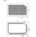
- FIG. 2A is a plan view showing the arrangement position of the non-magnetic body portion with respect to the coil conductor, and
- FIG. 2B is a plan view showing the arrangement position of the gap with respect to the coil conductor.
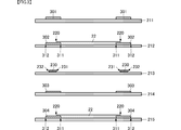
- FIG. 3 is a diagram showing a partial layer structure of the element body.
- the electronic component 10 includes an element body 20 and mounting-type elements 51 and 52.
- the mounted elements 51 and 52 are ICs, capacitors, and the like.
- the element body 20 includes a magnetic part 21 and non-magnetic parts 22, 24, and 25.
- the element body 20 has a substantially rectangular parallelepiped shape, and has a top surface and a bottom surface facing each other, and four side surfaces connecting the top surface and the bottom surface.
- the magnetic body portion 21, the nonmagnetic body portion 24, and the nonmagnetic body portion 25 have the same shape in plan view (viewed along the thickness direction), and are nonmagnetic from the top surface side to the bottom surface side of the element body 20.
- the body 24, the magnetic body 21, and the nonmagnetic body 25 are stacked in this order.
- the nonmagnetic body portion 22 is disposed at a midway position in the thickness direction of the magnetic body portion 21. The specific shape and arrangement of the nonmagnetic part 22 will be described later.
- the electronic component 10 further includes coil conductors 301, 302, 303, 304, wiring conductors 401, 402, 421, 422, 431, 432, 451, 452, 461, 462, terminal conductors 411, 412 for external connection, and , Element land conductors 441 and 442 are provided.
- the coil conductors 301, 302, 303, and 304 are disposed on the magnetic body portion 21.
- the coil conductors 301, 302, 303, and 304 are annular conductors that are partially divided in plan view.
- the coil conductors 301, 302, 303, and 304 are arranged at intervals along the thickness direction of the magnetic body portion 21.
- the coil conductors 301, 302, 303, and 304 are arranged so as to substantially overlap in a plan view.
- the coil conductors 301, 302, 303, and 304 are connected so as to form one spiral through an interlayer connection conductor for coils (not shown in FIG. 1).
- the coil conductors 301, 302, 303, 304 have winding axes parallel to the thickness direction of the magnetic body portion 21 and have openings inside the coil conductors 301, 302, 303, 304 in plan view.
- a coil pattern is formed.
- the wiring conductors 421, 422, 451, 452 are conductors extending in a direction orthogonal to the thickness direction of the element body 20.
- the wiring conductors 421 and 422 are formed at the interface between the magnetic part 21 and the nonmagnetic part 25.
- the wiring conductors 451 and 452 are formed at the interface between the magnetic part 21 and the nonmagnetic part 24.
- the wiring conductors 401, 402, 431, 432, 461, and 462 are columnar conductors that extend along the thickness direction of the element body 20.
- the wiring conductors 401 and 402 are formed in the magnetic part 21 and penetrate the magnetic part 21 in the thickness direction.
- the wiring conductors 431 and 432 are formed in the nonmagnetic body portion 25 and penetrate the nonmagnetic body portion 25 in the thickness direction.
- the wiring conductors 461 and 462 are formed in the nonmagnetic body portion 24 and penetrate the nonmagnetic body portion 24 in the thickness direction.
- the element land conductors 441 and 442 are formed on the top surface of the element body 20.
- the mountable element 51 is mounted on the element land conductor 441, and the mountable element 52 is mounted on the element land conductor 442.
- the terminal conductors 411 and 412 are formed on the bottom surface of the element body 20.
- the terminal conductor 411 is connected to the element land conductor 441 via the wiring conductor 431, the wiring conductor 421, the wiring conductor 401, the wiring conductor 451, and the wiring conductor 461.
- the terminal conductor 412 is connected to the element land conductor 442 through the wiring conductor 432, the wiring conductor 422, the wiring conductor 402, the wiring conductor 452, and the wiring conductor 462.
- These conductors are conductors for connecting the mountable elements 51 and 52 to an external ground, and are formed so as to avoid the above-described coil pattern formation region. That is, the terminal conductors 411 and 412 correspond to the ground terminal of the present invention, and the wiring conductors 421 and 422 correspond to the ground connection conductor of the present invention. Note that other conductive patterns (not shown) are formed on the element body 20, thereby realizing a function (for example, a DCDC converter) as the electronic component 10.
- a function for example, a DCDC converter
- the nonmagnetic part 22 is arranged at the same position as the coil conductor 302 and the same position as the coil conductor 304 in the thickness direction of the magnetic part 21.
- the thickness of the non-magnetic part 22 is appropriately set according to the coil characteristics such as the inductance of the coil realized by the element body 20 and the DC superposition characteristics.
- the thickness of the non-magnetic part 22 is preferably larger than the thickness of the coil conductors 302 and 304.
- the nonmagnetic body portion 22 has a flat film shape.
- the nonmagnetic body portion 22 has a shape that extends to the entire inner region surrounded by the coil conductor 302. Furthermore, the nonmagnetic body portion 22 overlaps a portion of the coil conductor 302 on the inner surface 311 side.
- the nonmagnetic part 22 is arranged so that the side end face 220 is between the inner side surface 311 and the outer side surface 312 of the coil conductor 302 in plan view.
- the positional relationship between the side end face 220 of the nonmagnetic body portion 22 and the inner side surface 311 and the outer side surface 312 of the coil conductor 302 is the same over the entire circumference of the coil conductor 302.
- the positional relationship between the coil conductor 304 and the nonmagnetic body portion 22 located at the same position in the thickness direction as the coil conductor 304 is also the same shape.
- the nonmagnetic part 22 is arranged in the entire area inside the coil pattern in a plan view. Thereby, the magnetic force lines passing through the inner side of the coil pattern always pass through the non-magnetic body portion 22, so that the DC superimposition characteristics are improved.
- the nonmagnetic body portion 22 overlaps with the coil conductor, even when the position of the nonmagnetic body portion 22 is shifted during the formation of the element body 20, the nonmagnetic body portion 22 is disposed on the inner side of the coil conductor. It is securely arranged over the entire area.
- the non-magnetic body portion 22 is not disposed between the coil pattern and the side surface of the element body 20.
- the width of the magnetic body between the coil pattern and the side surface of the element body 20 can be ensured to the maximum within the range of the dimensions of the element body 20. Therefore, the concentration of the magnetic field between the coil pattern and the element body 20 is suppressed, the magnetic saturation is hardly caused, and the direct current superimposition characteristic is improved.
- the nonmagnetic part 22 is not exposed on the side surface of the element body 20, it is possible to suppress noise generated from the coil pattern from leaking to the outside from the side surface of the element body 20.
- the air gap 23 is disposed at a position that does not overlap the non-magnetic part 22 in plan view. At this time, the wall surface 231 inside the gap 23 and the side end face 220 of the nonmagnetic body portion 22 coincide with each other in plan view.
- the gap 23 has a shape that extends in the same manner along the direction in which the coil conductor 302 extends. That is, in the plan view, the gap 23 has a shape surrounding the nonmagnetic part 22.
- the flatness of the top surface of the element body 20 can be improved.
- the mounting elements 51 and 52 can be easily mounted, and the mounting reliability is improved.
- the flatness of the top surface of the element body 20 may be realized at least in the arrangement region of the element land conductors 441 and 442.
- the gap 23 the stress relating to the magnetic part 21 is relieved. Thereby, the loss of the magnetic part 21 can be suppressed.
- the gap 23 overlaps the coil conductor 302 in plan view.
- the inner wall surface 231 forming the air gap 23 is closer to the outer surface 312 than the inner surface 311 of the coil conductor 302, and the outer wall surface 232 forming the air gap 23 is outside the coil conductor 302. It is on the inner side 311 side than the side 312.
- gap 23 is not arrange
- the gap 23 is arranged between the coil conductor 302 and the coil conductor 303 in the thickness direction of the magnetic body portion 21. That is, the air gap 23 is arranged on the side different from the nonmagnetic body portion 22 in the thickness direction of the element body 20 with respect to the lower surface of the coil conductor 302. Thereby, it can prevent that the nonmagnetic body part 22 and the space
- the gap 23 is not in direct contact with the coil conductor 302 and the coil conductor 303, and is surrounded by the magnetic body forming the magnetic body portion 21. Thereby, it is further prevented that the nonmagnetic body portion 22 and the gap 23 are in direct contact with each other.
- the non-magnetic body portion 22 is symmetrically arranged on the top surface side and the back surface side of the element body 20 with respect to the position of the gap 23.
- the portion of the magnetic body portion 21 of the element body 20 having such a configuration is manufactured as follows. It should be noted that the portions of the element body 20 other than the nonmagnetic portions 24 and 25 and the coil conductors 301, 302, 303, and 304 can be manufactured by a known method for manufacturing a laminated ferrite element, and illustration and description thereof are omitted. To do.
- a plurality of magnetic sheets 211, 212, 213, 214, 215 are prepared.
- the coil conductor 301 is printed on the surface of the magnetic sheet 211
- the coil conductor 302 is printed on the surface of the magnetic sheet 212
- the coil conductor 303 is printed on the surface of the magnetic sheet 214
- the coil is printed on the surface of the magnetic sheet 215.
- the conductor 304 is printed.
- the non-magnetic part 22 is printed on the surface of the magnetic sheet 212 on which the coil conductor 302 is printed.
- the nonmagnetic body portion 22 covers the entire area inside the coil conductor 302, and the side end surface 220 of the nonmagnetic body portion 22 is disposed between the inner side surface 311 and the outer side surface 312 of the coil conductor 302. That is, it is printed so as to overlap the coil conductor 302.
- the non-magnetic part 22 is printed on the surface of the magnetic sheet 215 on which the coil conductor 304 is printed.
- the nonmagnetic body portion 22 covers the entire inner area of the coil conductor 304, and the side end surface 220 of the nonmagnetic body portion 22 is disposed between the inner side surface 311 and the outer side surface 312 of the coil conductor 304. That is, it is printed so as to overlap the coil conductor 304.
- the baking disappearance paste 230 corresponding to the shape of the gap 23 is printed on the surface of the magnetic sheet 213.
- the burnt-off paste 230 is printed at a position that overlaps with the coil conductors 301, 302, 303, and 304 in the other magnetic sheets 211, 212, 214, and 215 and does not overlap with the nonmagnetic body portion 22.
- these magnetic sheets 211, 212, 214, 215 are laminated and fired.
- the firing disappearing paste 230 disappears, and a gap 23 is formed between the coil conductor 302 and the coil conductor 303.
- the element body 20 including the above-described non-magnetic body portion 22 and having the voids 23 formed therein.
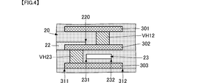
- FIG. 4 is a diagram showing a partially enlarged cross-sectional structure showing an example of an arrangement of interlayer connection conductors.
- the coil conductor 304 is not shown, but the interlayer connection conductor formation pattern for the coil conductor 304 can be realized by the same principle as the interlayer connection conductor formation pattern for the coil conductor 302. Good.
- the interlayer connection conductor VH12 that connects the coil conductor 301 and the coil conductor 302 is disposed at a position that does not overlap the nonmagnetic body portion 22 in plan view. Thereby, it is not necessary to provide a hole for the interlayer connection conductor VH12 from the side opposite to the surface in contact with the coil conductor 302, and the interlayer connection conductor VH12 can be easily formed.
- the nonmagnetic part 22 is not disposed between the coil conductor 302 and the coil conductor 303. Therefore, the interlayer connection conductor VH23 that connects the coil conductor 302 and the coil conductor 303 may be formed at any position except for the portion where the gap 23 is formed. That is, as shown in FIG. 4, the interlayer connection conductor VH ⁇ b> 23 may overlap with the nonmagnetic body portion 22 in plan view. Thereby, the arrangement
- FIG. 5 is a side sectional view showing a schematic configuration of an electronic component according to the second embodiment of the present invention.
- the electronic component 10A according to the second embodiment is different from the electronic component 10 according to the first embodiment in the position where the air gap 23A is formed, the shape of the air gap 23A, and the nonmagnetic part. 22 differs in the number of formations.
- Other configurations of the electronic component 10 ⁇ / b> A are the same as those of the electronic component 10, and descriptions of the same parts are omitted.
- the element body 20 is provided with one nonmagnetic body portion 22.
- the nonmagnetic part 22 is disposed at the same position as the coil conductor 302 in the thickness direction of the magnetic part 21.
- the gap 23 ⁇ / b> A is disposed between the coil conductor 302 and the coil conductor 303, and the inner wall surface 231 is separated from the side end face 220 of the nonmagnetic body portion 22 in plan view.
- the height of the gap 23 ⁇ / b> A is set according to the thickness of one nonmagnetic body portion 22.
- the electronic component 10A having a good DC superimposition characteristic can be realized.
- FIG. 6 is a side sectional view showing a schematic configuration of an electronic component according to the third embodiment of the present invention.
- the electronic component 10B according to the third embodiment is different from the electronic component 10A according to the second embodiment in the formation position of the air gap 23B, the shape of the air gap 23B, and the nonmagnetic part. 22 is different in the formation position.
- the other configuration of the electronic component 10B is the same as that of the electronic component 10A, and the description of the same part is omitted.
- the element body 20 is provided with one nonmagnetic body portion 22.
- the nonmagnetic body portion 22 is disposed at the same position as the coil conductor 303 in the thickness direction of the magnetic body portion 21.
- the air gap 23B is formed in the coil conductor 302 (corresponding to the first coil conductor in the claims) and the coil conductor 303 (corresponding to the second coil conductor in the claims) disposed adjacent to each other in the thickness direction of the element body 20. Equivalent). That is, the gap 23 ⁇ / b> B and a part of the non-magnetic body portion 22 are both disposed between the coil conductor 302 and the coil conductor 303.
- the gap 23 ⁇ / b> B overlaps the coil conductor 302 and the coil conductor 303 in the thickness direction of the element body 20.
- the gap 23 ⁇ / b> B does not need to completely overlap the coil conductor 302 and the coil conductor 303 in the thickness direction of the element body 20.
- the position of the gap 23 ⁇ / b> B in the thickness direction of the element body 20 does not match the position of the nonmagnetic body portion 22.
- the wall surface 231 inside the air gap 23 ⁇ / b> B is separated from the side end surface 220 of the nonmagnetic body portion 22 in plan view. As a result, the air gap 23B and the nonmagnetic part 22 are not in direct contact with each other, and the magnetic substance is interposed therebetween.
- an electronic component 10B having good direct current superposition characteristics can be realized in the same manner as the electronic component 10A according to the second embodiment described above.
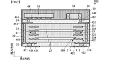
- FIG. 7 is a side sectional view showing a schematic configuration of an electronic component according to the fourth embodiment of the present invention.
- the electronic component 10C according to the fourth embodiment is different from the electronic component 10 according to the first embodiment in that a resin cover 60 and a conductive layer 70 are added.
- Other configurations of the electronic component 10 ⁇ / b> C are the same as those of the electronic component 10, and the description of the same parts is omitted. Note that the configuration of the present embodiment can also be applied to the configurations of the second and third embodiments described above.
- the electronic component 10 ⁇ / b> C includes a resin cover 60 and a conductive layer 70.
- the resin cover 60 is made of an insulating resin.
- the resin cover 60 covers the top surface of the element body 20 and the mounting type elements 51 and 52.
- the conductive layer 70 covers the entire top and side surfaces of the resin cover 60 and the side surfaces of the element body 20.
- the conductive layer 70 is connected to the wiring conductors 421 and 422 on the side surface of the element body 20.
- noise radiated to the top surface side of the element body 20, such as noise radiated from the mounting elements 51 and 52, and noise radiated from the side surface of the element body 20 are reduced. Can lead to the ground. Thereby, the radiation
- the frequency range of noise radiated to the outside can be adjusted by adjusting the thickness of the conductive layer 70. For example, by increasing the thickness of the conductive layer 70, not only high frequency but also low frequency noise emission can be suppressed.
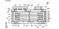
- FIG. 8 is a side sectional view showing a schematic configuration of an electronic component according to the fifth embodiment of the present invention.
- the wiring conductors 403, 423, 453, and 463 penetrate through the nonmagnetic part 22 with respect to the electronic component 10 according to the first embodiment. Are different in that they are arranged.
- the other configuration of the electronic component 10D is the same as that of the electronic component 10, and the description of the same part is omitted. Note that the configuration of the present embodiment is also applicable to the configurations of the second, third, and fourth embodiments described above.
- the wiring conductor 403 has a shape penetrating the magnetic body portion 21 and the non-magnetic body portion 22.
- the wiring conductor 403 is formed in a region inside the coil conductors 301, 302, 303, and 304 in the plan view, that is, in the opening of the coil pattern in the plan view.
- the wiring conductor 403 is made of a nonmagnetic conductor, and is made of, for example, copper or silver.
- the wiring conductor 423 is a conductor extending in a direction orthogonal to the thickness direction of the element body 20, and is formed at the interface between the magnetic body portion 21 and the nonmagnetic body portion 25.
- the wiring conductor 453 is a conductor that extends in a direction orthogonal to the thickness direction of the element body 20, and is formed at the interface between the magnetic body portion 21 and the nonmagnetic body portion 24.
- the wiring conductor 463 is formed in the nonmagnetic body portion 24 and penetrates the nonmagnetic body portion 24 in the thickness direction.
- the element land conductor 441D on which the mounting type element 51 is mounted is connected to the wiring conductor 463, the wiring conductor 453, the wiring conductor 403, the wiring conductor 423, and the wiring conductor (not shown) formed in the nonmagnetic body portion 25.
- the terminal conductors are not shown.
- the wiring conductor 403 is close to the center of the opening of the coil pattern in a plan view and is separated from the coil conductors 301, 302, 303, and 304. Thereby, the bad influence to the characteristic of a coil pattern can be suppressed.
- wiring conductor for the mounting element 51 is arranged in the opening of the coil pattern.
- wiring conductors for other mounting-type elements arranged on the top surface of the element body 20 such as the mounting-type element 52 can also be arranged in the opening of the coil pattern, and the above-described effects can be obtained.
- the gap 23 is formed at only one place in the thickness direction of the element body 20.
- a plurality of gaps 23 may be formed in the thickness direction of the element body 20.
- the mounting elements 51 and 52 are electronic components mounted on the top surface of the element body 20, but only the part of the element body 20, that is, a single coil component, is also described above. Can be applied.
- the non-magnetic body portion 22 is disposed in a plurality of layers.
- the thickness corresponding to the total thickness of the plurality of non-magnetic body portions 22 is set. It is also possible to use one non-magnetic member 22 having the same.
- the thickness of one nonmagnetic body portion 22 can be reduced by using a plurality of nonmagnetic body portions 22, and the distance between the plurality of coil conductors arranged with the nonmagnetic body portion 22 interposed therebetween is different from the other coil conductors. It can be suppressed that the distance is significantly larger than the distance between them. That is, it is easy to arrange a plurality of coil conductors at substantially equal intervals in the thickness direction. Thereby, a coil having a desired inductance can be easily formed.
Landscapes
- Engineering & Computer Science (AREA)
- Microelectronics & Electronic Packaging (AREA)
- Power Engineering (AREA)
- Manufacturing & Machinery (AREA)
- Coils Or Transformers For Communication (AREA)
- Parts Printed On Printed Circuit Boards (AREA)
Abstract
優れた直流重畳特性を有する電子部品を確実に実現する。電子部品(10)は、素体(20)およびコイル導体(301-304)を備える。素体(20)は、磁性体部(21)と非磁性体部(22、24、25)とを備える。コイル導体(301-304)は、磁性体部(21)に配置され、天面および底面に直交する方向に視て、部分的に分断された環状からなる。天面および底面に直交する方向に視て、非磁性体部(22)は、コイル導体の(301-304)内側の全領域に広がる形状である。且つ、非磁性体部(22)の側端面(220)は、コイル導体(302、304)の内側面(311)と外側面(312)との間に配置されている。
Description
本発明は、内部にコイル導体が形成された磁性体を含む素体を有する電子部品に関する。
従来、巻回形のコイル導体を磁性体内に形成した電子部品が各種考案されている。そして、特許文献1および特許文献2に記載の電子部品は、磁性体の内部に非磁性体を備えている。
特許文献1に記載の電子部品は、次の二種類の構成のいずれかを備える。第1の構成として、非磁性体は、磁性体における巻回形のコイル導体の内側の領域に配置されている。この際、非磁性体は、コイル導体の巻回軸に平行な方向に視て、コイル導体の内側の領域の中央部に配置されている。また、第2の構成として、非磁性体は、コイル導体の全体を覆い、且つ、コイル導体の巻回軸に平行な方向に視て、コイル導体の内側の領域の全体に広がる形状で配置されている。また、この非磁性体は、コイル導体の外側の領域であってコイル導体と磁性体の側面との間の領域まで広がる形状で配置されている。
特許文献2に記載の電子部品では、非磁性体は、コイル導体の巻回軸に平行な方向に視て、コイル導体の内側の領域の全体に広がる形状で配置されている。
しかしながら、特許文献1に記載の電子部品における第1の構成では、コイル導体の内側に非磁性体が無い領域が存在する。したがって、電子部品の直流重畳特性は、悪くなる。また、特許文献1に記載の電子部品における第2の構成では、コイル導体と磁性体の側面との間の磁性体の幅が狭くなり、直流重畳特性は、悪くなる。
また、特許文献2に記載の電子部品では、製造誤差によって、コイル導体の巻回軸に平行な方向に視て、コイル導体の内側に非磁性体が無い部分が発生することがある。このように、非磁性体が無い部分が存在すると、電子部品の直流重畳特性は、悪くなる。
したがって、本発明の目的は、優れた直流重畳特性を有する電子部品を確実に実現することにある。
本発明の電子部品は、素体およびコイル導体を備える。素体は、互いに対向する天面および底面と、天面および底面を繋ぐ側面と、を有する。素体は、磁性体部と非磁性体部とを備える。コイル導体は、磁性体部に配置され、天面および底面に直交する方向に視て、部分的に分断された環状からなり、磁性体部に配置されるコイル導体の個数は1個以上である。天面および底面に直交する方向に視て、非磁性体部は、コイル導体の内側の全領域に広がる形状である。且つ、非磁性体部の側端面は、コイル導体の外側面と内側面との間に配置されている。
この構成では、非磁性体部は、コイル導体の内側の全領域に広がり、且つ、非磁性体部の側端面付近は、コイル導体に重なる。したがって、非磁性体部は、コイル導体の内側の全領域に確実に配置される。
また、この発明の電子部品では、天面および底面に直交する方向に視て、磁性体部は、コイル導体に重なり、且つ、非磁性体部に重ならない位置に、空隙を有することが好ましい。
この構成では、非磁性体部が存在する領域と非磁性体部が存在しない領域との素体の厚みの差が空隙によって緩和される。また、この空隙によって、素体に係る応力が緩和され、磁性体部に係る応力が緩和される。
また、この発明の電子部品では、天面および底面に直交する方向に視て、非磁性体部の側端面と、磁性体部に形成された空隙の非磁性体部に近い側の端面と、は一致していることが好ましい。
この構成では、素体の天面の平坦度がさらに向上する。
また、この発明の電子部品では、素体の厚み方向における非磁性体部の位置と磁性体部に形成された空隙の位置とは、異なっていることが好ましい。
この構成では、非磁性体部と空隙とが隣り合わない構成が、容易に実現される。
また、この発明の電子部品では、コイル導体は、磁性体部の厚み方向に沿って間隔を空けて複数配置されており、厚み方向において、非磁性体部と磁性体部に形成された空隙とは、複数のコイル導体における1つのコイル導体の一主面に対して、異なる側に配置されていることが好ましい。
この構成では、非磁性体部と空隙とが隣り合わない構成が、さらに容易且つ確実に実現される。
また、この発明の電子部品では、コイル導体は、磁性体部の厚み方向に沿って、間隔を空けて複数配置されており、素体の厚み方向において、隣接して配置される第1コイル導体と第2コイル導体とを有し、第1コイル導体と第2コイル導体との間に、非磁性体部と、磁性体部に形成された空隙と、が配置されていることが好ましい。
この構成では、非磁性体部と空隙とが隣り合わない構成が、より容易且つ確実に実現される。
また、この発明の電子部品は、実装型素子、樹脂カバー、導電層、グランド端子、および、グランド接続用導体を備える。実装型素子は、素体の天面に実装されている。樹脂カバーは、素体の天面および実装型素子を覆っている。導電層は、樹脂カバー、および、素体の側面の少なくとも一部を覆っている。グランド端子は、素体の底面に形成されている。グランド接続用導体は、素体に形成され、導電層とグランド端子とを接続する。
この構成では、実装型素子から放射されるノイズが導電層およびグランド接続用導体を介して、グランド端子に導かれる。
この発明によれば、優れた直流重畳特性を有する電子部品を実現できる。
本発明の第1の実施形態に係る電子部品について、図を参照して説明する。図1は、本発明の第1の実施形態に係る電子部品の概略構成を示す側面断面図である。図2(A)は、コイル導体に対する非磁性体部の配置位置を示す平面図であり、図2(B)は、コイル導体に対する空隙の配置位置を示す平面図である。図3は、素体の一部の層構造を示す図である。
図1に示すように、電子部品10は、素体20、および、実装型素子51、52を備える。実装型素子51、52は、IC、キャパシタ等である。
素体20は、磁性体部21、非磁性体部22、24、25を備える。素体20は、略直方体形状であり、互いに対向する天面と底面、および、天面と底面とを繋ぐ四個の側面を有する。磁性体部21、非磁性体部24、非磁性体部25は、平面視において(厚み方向に沿って視て)、同じ形状であり、素体20の天面側から底面側に、非磁性体部24、磁性体部21、非磁性体部25の順に積層して配置されている。非磁性体部22は、磁性体部21における厚み方向の途中位置に配置されている。非磁性体部22の具体的な形状および配置は後述する。
電子部品10は、さらに、コイル導体301、302、303、304、配線導体401、402、421、422、431、432、451、452、461、462、外部接続用の端子導体411、412、および、素子用ランド導体441、442を備える。
コイル導体301、302、303、304は、磁性体部21に配置されている。コイル導体301、302、303、304は、平面視において、部分的に分断された環状の導体である。コイル導体301、302、303、304は、磁性体部21の厚み方向に沿って間隔を空けて配置されている。コイル導体301、302、303、304は、平面視において、略重なるように配置されている。コイル導体301、302、303、304は、コイル用の層間接続導体(図1では図示を省略している。)を介して、1本の螺旋を形成するように接続されている。この構成によって、コイル導体301、302、303、304は、磁性体部21の厚み方向に平行な巻回軸を有し、平面視においてコイル導体301、302、303、304の内側に開口を有するコイルパターンを形成している。
配線導体421、422、451、452は、素体20の厚み方向に直交する方向へ延びる導体である。配線導体421、422は、磁性体部21と非磁性体部25との界面に形成されている。配線導体451、452は、磁性体部21と非磁性体部24との界面に形成されている。配線導体401、402、431、432、461、462は、素体20の厚み方向に沿って延びる柱状の導体である。配線導体401、402は、磁性体部21に形成されており、磁性体部21を厚み方向に貫通している。配線導体431、432は、非磁性体部25に形成されており、非磁性体部25を厚み方向に貫通している。配線導体461、462は、非磁性体部24に形成されており、非磁性体部24を厚み方向に貫通している。
素子用ランド導体441、442は、素体20の天面に形成されている。実装型素子51は、素子用ランド導体441に実装されており、実装型素子52は、素子用ランド導体442に実装されている。
端子導体411、412は、素体20の底面に形成されている。端子導体411は、配線導体431、配線導体421、配線導体401、配線導体451、および、配線導体461を介して、素子用ランド導体441に接続されている。端子導体412は、配線導体432、配線導体422、配線導体402、配線導体452、および、配線導体462を介して、素子用ランド導体442に接続されている。
これらの導体は、実装型素子51、52を外部のグランドに接続するための導体であり、上述のコイルパターンの形成領域を避けて形成されている。すなわち、端子導体411、412は、本発明のグランド端子に対応し、配線導体421、422は、本発明のグランド接続用導体に対応する。なお、素体20には、図示を省略している他の導体パターンが形成されており、これらにより、電子部品10としての機能(例えば、DCDCコンバータ)を実現している。
次に、非磁性体部22とコイル導体301、302、303、304との位置関係について、より具体的に説明する。
図1、図3に示すように、非磁性体部22は、磁性体部21の厚み方向におけるコイル導体302と同じ位置と、コイル導体304と同じ位置と、に配置されている。非磁性体部22の厚みは、素体20で実現するコイルのインダクタンス、直流重畳特性等のコイル特性に応じて適宜設定されている。ただし、非磁性体部22の厚みは、コイル導体302、304の厚みよりも大きいことが好ましい。
図1、図2(A)、図3に示すように、非磁性体部22は、平膜状である。非磁性体部22は、コイル導体302によって囲まれる内側の全領域に広がる形状である。さらに、非磁性体部22は、コイル導体302の内側面311側の部分に重なっている。言い換えれば、平面視において、非磁性体部22は、側端面220がコイル導体302の内側面311と外側面312との間となるように、配置されている。
この非磁性体部22の側端面220とコイル導体302の内側面311および外側面312との位置関係は、コイル導体302の全周に亘って同様である。コイル導体304と、当該コイル導体304と厚み方向において同じ位置にある非磁性体部22との位置関係も同じ形状である。
このような構成によって、平面視において、コイルパターンの内側の全領域には、非磁性体部22が配置される。これにより、コイルパターンの内側を通る磁力線は、必ず非磁性体部22を通過するので、直流重畳特性が良好になる。
さらに、非磁性体部22がコイル導体と重なっていることによって、素体20の形成の際に、非磁性体部22の位置がズレても、非磁性体部22が、コイル導体の内側の全領域に亘って確実に配置される。
また、さらに、非磁性体部22は、コイルパターンと素体20の側面との間に配置されていない。これにより、コイルパターンと素体20の側面との磁性体の幅を、素体20の寸法の範囲において最大に確保できる。したがって、コイルパターンと素体20との間の磁場の集中を抑制し、磁気飽和し難く、直流重畳特性が良好になる。
さらに、非磁性体部22は、素体20の側面に露出していないので、コイルパターンから発生するノイズが素体20の側面から外部に漏洩することを抑制できる。
次に、磁性体部21に形成された空隙23について、具体的に説明する。
空隙23は、平面視において、非磁性体部22と重ならない位置に配置されている。この際、平面視において、空隙23の内側の壁面231と非磁性体部22の側端面220とは一致している。
また、図2(B)に示すように、空隙23は、コイル導体302の延びる方向に沿って同じように延びる形状である。すなわち、平面視において、空隙23は、非磁性体部22を囲む形状である。
このような構成によって、非磁性体部22を内蔵することによる素体20の天面に凹凸が生じることを、空隙23によって抑制できる。すなわち、素体20の天面の平坦性を向上できる。これにより、実装型素子51、52の実装を容易にでき、実装の信頼性が向上する。なお、素体20の天面の平坦性は、少なくとも、素子用ランド導体441、442の配置領域で実現していればよい。
また、空隙23を形成することによって、磁性体部21に係る応力が緩和される。これにより、磁性体部21の損失を抑制できる。
また、図2(B)に示すように、平面視において、空隙23は、コイル導体302に重なっている。言い換えれば、平面視において、空隙23を形成する内側の壁面231は、コイル導体302の内側面311よりも外側面312側にあり、空隙23を形成する外側の壁面232は、コイル導体302の外側面312よりも内側面311側にある。これにより、空隙23がコイルパターンと素体20の側面との間の領域に配置されず、この領域の磁性体部21の幅が小さくなることを防止できる。したがって、直流重畳特性が向上する。
また、空隙23は、磁性体部21の厚み方向において、コイル導体302とコイル導体303との間に配置されている。すなわち、空隙23は、コイル導体302の下面を基準にして、素体20の厚み方向において、非磁性体部22と異なる側に配置されている。これにより、非磁性体部22と空隙23とが直接に接することが防止でき、素体20の焼成時に、非磁性体部22にクラックが発生することを抑制できる。したがって、信頼性の高い電子部品10を実現できる。
さらに、この際、空隙23は、コイル導体302とコイル導体303とに対して直接接しておらず、磁性体部21を形成する磁性体によって囲まれている。これにより、非磁性体部22と空隙23とが直接に接することがさらに防止される。
また、電子部品10では、素体20は、空隙23の位置を基準にして、天面側と裏面側とで非磁性体部22が対称に配置されている。このような構成とすることによって、素体20に加わる応力が均一化し、部分的に大きな応力が加わることを抑制できる。
このような構成の素体20の磁性体部21の部分は、次に示すように製造される。なお、素体20における非磁性体部24、25の部分およびコイル導体301、302、303、304以外の箇所は、既知の積層型フェライト素子の製造方法によって製造可能であり、図示および説明は省略する。
図3に示すように、複数の磁性体シート211、212、213、214、215を用意する。磁性体シート211の表面にコイル導体301を印刷し、磁性体シート212の表面にコイル導体302を印刷し、磁性体シート214の表面にコイル導体303を印刷し、磁性体シート215の表面にコイル導体304を印刷する。
コイル導体302が印刷された磁性体シート212の表面に、非磁性体部22を印刷する。非磁性体部22は、コイル導体302の内側の全領域を覆い、且つ、非磁性体部22の側端面220がコイル導体302の内側面311と外側面312との間に配置されるように、すなわち、コイル導体302に重なるように、印刷されている。
コイル導体304が印刷された磁性体シート215の表面に、非磁性体部22を印刷する。非磁性体部22は、コイル導体304の内側の全領域を覆い、且つ、非磁性体部22の側端面220がコイル導体304の内側面311と外側面312との間に配置されるように、すなわち、コイル導体304に重なるように、印刷されている。
磁性体シート213の表面に、空隙23の形状に応じた焼成消失ペースト230を印刷する。焼成消失ペースト230は、他の磁性体シート211、212、214、215におけるコイル導体301、302、303、304と重なり、非磁性体部22に重ならない位置に印刷されている。
次に、これらの磁性体シート211、212、214、215を積層して焼成する。この焼成によって、焼成消失ペースト230は消失し、コイル導体302とコイル導体303との間に空隙23が形成される。
このような製造方法を用いることによって、上述の非磁性体部22を備え、空隙23が形成された素体20を、容易に製造できる。
なお、上述のように、コイル導体301、302、303、304は、コイル用の層間接続導体によって接続されている。この際、層間接続導体は、図4に示す構成を採用していればよい。図4は、層間接続導体の配置の一態様例を示す部分拡大の断面構造を示す図である。なお、図4では、コイル導体304の部分は図示を省略しているが、コイル導体304に対する層間接続導体の形成パターンは、コイル導体302に対する層間接続導体の形成パターンと同様の原理で実現すればよい。
コイル導体301とコイル導体302との間には、部分的に非磁性体部22が配置されている。したがって、コイル導体301とコイル導体302とを接続する層間接続導体VH12は、平面視において、非磁性体部22と重ならない位置に配置されている。これにより、非磁性体部22に対して、コイル導体302に当接する面と反対側から層間接続導体VH12用の孔を設ける必要が無く、層間接続導体VH12を容易に形成できる。
コイル導体302とコイル導体303との間には、非磁性体部22が配置されていない。したがって、コイル導体302とコイル導体303とを接続する層間接続導体VH23は、空隙23の形成部を除いて、どの位置に形成してもよい。すなわち、図4に示すように、平面視において、層間接続導体VH23は、非磁性体部22と重なっていてもよい。これにより、層間接続導体VH23の配置自由度が向上する。
次に、本発明の第2の実施形態に係る電子部品について、図を参照して説明する。図5は、本発明の第2の実施形態に係る電子部品の概略構成を示す側面断面図である。
図5に示すように、第2の実施形態に係る電子部品10Aは、第1の実施形態に係る電子部品10に対して、空隙23Aの形成位置、空隙23Aの形状、および、非磁性体部22の形成数において異なる。電子部品10Aの他の構成は、電子部品10と同様であり、同様の箇所の説明は省略する。
素体20には、1個の非磁性体部22が配置されている。非磁性体部22は、磁性体部21の厚み方向におけるコイル導体302と同じ位置に配置されている。空隙23Aは、コイル導体302とコイル導体303との間に配置されており、平面視において、内側の壁面231は、非磁性体部22の側端面220と離間している。空隙23Aの高さは、1個の非磁性体部22の厚みに応じて設定されている。
このような構成であっても、上述の第1の実施形態に係る電子部品10と同様に、直流重畳特性の良好な電子部品10Aを実現できる。
次に、本発明の第3の実施形態に係る電子部品について、図を参照して説明する。図6は、本発明の第3の実施形態に係る電子部品の概略構成を示す側面断面図である。
図6に示すように、第3の実施形態に係る電子部品10Bは、第2の実施形態に係る電子部品10Aに対して、空隙23Bの形成位置、空隙23Bの形状、および、非磁性体部22の形成位置において異なる。電子部品10Bの他の構成は、電子部品10Aと同様であり、同様の箇所の説明は省略する。
素体20には、1個の非磁性体部22が配置されている。非磁性体部22は、磁性体部21の厚み方向におけるコイル導体303と同じ位置に配置されている。空隙23Bは、素体20の厚み方向において、互いに隣接して配置されるコイル導体302(特許請求の範囲における第1コイル導体に相当)とコイル導体303(特許請求の範囲における第2コイル導体に相当)との間に配置されている。すなわち、空隙23Bと、非磁性体部22の一部とは、ともにコイル導体302とコイル導体303との間に配置されている。空隙23Bは、素体20の厚み方向において、コイル導体302とコイル導体303とに重なっている。ただし、空隙23Bは、素体20の厚み方向において、コイル導体302とコイル導体303とに完全に重なっている必要はない。しかしながら、素体20の厚み方向における空隙23Bの位置と非磁性体部22の位置とは一致していない。さらに、平面視において、空隙23Bの内側の壁面231は、非磁性体部22の側端面220と離間している。これにより、空隙23Bと非磁性体部22とは直接接することなく、これらの間に磁性体が介在する。
このような構成であっても、上述の第2の実施形態に係る電子部品10Aと同様に、直流重畳特性の良好な電子部品10Bを実現できる。
次に、本発明の第4の実施形態に係る電子部品について、図を参照して説明する。図7は、本発明の第4の実施形態に係る電子部品の概略構成を示す側面断面図である。
図7に示すように、第4の実施形態に係る電子部品10Cは、第1の実施形態に係る電子部品10に対して、樹脂カバー60および導電層70を追加した点において異なる。電子部品10Cの他の構成は、電子部品10と同様であり、同様の箇所の説明は省略する。なお、本実施形態の構成は、上述の第2、第3の実施形態の構成にも適用可能である。
電子部品10Cは、樹脂カバー60および導電層70を備える。
樹脂カバー60は、絶縁性の樹脂からなる。樹脂カバー60は、素体20の天面および実装型素子51、52を覆っている。
導電層70は、樹脂カバー60の天面および側面の全面と、素体20の側面とを覆っている。導電層70は、素体20の側面において配線導体421、422に接続している。
このような導電層70を配置することによって、実装型素子51、52から放射されるノイズ等の素体20の天面側へ放射されるノイズ、および、素体20の側面から放射するノイズを、グランドに導くことができる。これにより、電子部品10Cが発生するノイズの外部への放射を抑制できる。この際、導電層70の厚みを調整することによって、外部へ放射されるノイズの周波数範囲を調整できる。例えば、導電層70の厚みを厚くすることによって、高周波だけでなく低周波のノイズの放射も抑制できる。
次に、本発明の第5の実施形態に係る電子部品について、図を参照して説明する。図8は、本発明の第5の実施形態に係る電子部品の概略構成を示す側面断面図である。
図8に示すように、第5の実施形態に係る電子部品10Dは、第1の実施形態に係る電子部品10に対して、配線導体403、423、453、463が非磁性体部22を貫くように配置された点において異なる。電子部品10Dの他の構成は、電子部品10と同様であり、同様の箇所の説明は省略する。なお、本実施形態の構成は、上述の第2、第3、第4の実施形態の構成にも適用可能である。
配線導体403は、磁性体部21および非磁性体部22を貫通する形状である。配線導体403は、平面視において、コイル導体301、302、303、304の内側の領域、すなわち、平面視におけるコイルパターンの開口内に形成されている。配線導体403は、非磁性の導体からなり、例えば、銅、または、銀等からなる。
配線導体423は、素体20の厚み方向に直交する方向へ延びる導体であり、磁性体部21と非磁性体部25との界面に形成されている。配線導体453は、素体20の厚み方向に直交する方向へ延びる導体であり、磁性体部21と非磁性体部24との界面に形成されている。配線導体463は、非磁性体部24に形成されており、非磁性体部24を厚み方向に貫通している。
実装型素子51が実装される素子用ランド導体441Dは、配線導体463、配線導体453、配線導体403、配線導体423、および、非磁性体部25に形成された図示を省略した配線導体を介して、図示を省略した端子導体に接続されている。
このような構成によって、実装型素子51への配線をコイルパターンの開口内に配置しながら、直流重畳特性の低下を抑制できる。すなわち、電子部品10Dを小型のまま、電子部品10Dの内部配線の自由度を向上でき、且つ、直流重畳特性の低下を抑制できる。
なお、配線導体403は、平面視におけるコイルパターンの開口の中心に近く、コイル導体301、302、303、304から離間していることが好ましい。これにより、コイルパターンの特性への悪影響を抑制できる。
また、この例では、実装型素子51に対する配線導体をコイルパターンの開口内に配置する態様を示した。しかしながら、実装型素子52等の素体20の天面に配置された他の実装型素子に対する配線導体をコイルパターンの開口内に配置することもでき、上述の作用効果を得られる。
なお、上述の各実施形態では、空隙23は、素体20の厚み方向に1箇所のみに形成される態様を示した。しかしながら、空隙23は、素体20の厚み方向に複数箇所形成されていてもよい。
また、上述の各実施形態では、実装型素子51、52が素体20の天面に実装される電子部品を示したが、素体20の部分のみ、すなわち、単体のコイル部品としても、上述の構成を適用できる。
また、上述の第1、第4、第5の実施形態では、非磁性体部22を複数層配置する態様を示したが、これら複数の非磁性体部22の合計の厚みに対応する厚みを有する1個の非磁性体部22を用いることも可能である。ただし、非磁性体部22を複数にすることによって、1個の非磁性体部22の厚みを薄くでき、非磁性体部22が挟んで配置される複数のコイル導体間距離が他のコイル導体間の距離よりも大幅に大きくなることを抑制できる。すなわち、厚み方向において複数のコイル導体を略等間隔に配置し易い。これにより、所望のインダクタンスとなるコイルを容易に形成できる。
10、10A、10B、10C、10D:電子部品
20:素体
21:磁性体部
22:非磁性体部
23、23A、23B:空隙
24、25:非磁性体部
51、52:実装型素子
60:樹脂カバー
70:導電層
211、212、213、214、215:磁性体シート
220:側端面
230:焼成消失ペースト
231:壁面
232:壁面
301、302、303、304:コイル導体
311:内側面
312:外側面
401、402、403、421、422、423、431、432、451、452、453、461、462、463:配線導体
411、412:端子導体
441、441D、442:素子用ランド導体
VH12、VH23:層間接続導体
20:素体
21:磁性体部
22:非磁性体部
23、23A、23B:空隙
24、25:非磁性体部
51、52:実装型素子
60:樹脂カバー
70:導電層
211、212、213、214、215:磁性体シート
220:側端面
230:焼成消失ペースト
231:壁面
232:壁面
301、302、303、304:コイル導体
311:内側面
312:外側面
401、402、403、421、422、423、431、432、451、452、453、461、462、463:配線導体
411、412:端子導体
441、441D、442:素子用ランド導体
VH12、VH23:層間接続導体
Claims (7)
- 互いに対向する天面および底面と、前記天面および前記底面を繋ぐ側面と、を有し、磁性体部と非磁性体部とを備える素体と、
前記磁性体部に配置され、前記天面および前記底面に直交する方向に視て、部分的に分断された環状からなる1個以上のコイル導体と、
を備え、
前記天面および前記底面に直交する方向に視て、前記非磁性体部は、前記コイル導体の内側の全領域に広がる形状であり、且つ、前記非磁性体部の側端面は、前記コイル導体の外側面と内側面との間に配置されている、
電子部品。 - 前記天面および前記底面に直交する方向に視て、
前記磁性体部は、前記コイル導体に重なり、且つ、前記非磁性体部に重ならない位置に、空隙を有する、
請求項1に記載の電子部品。 - 前記天面および底面に直交する方向に視て、
前記非磁性体部の側端面と、前記磁性体部に形成された前記空隙の前記非磁性体部に近い側の端面と、は一致している、
請求項2に記載の電子部品。 - 前記素体の厚み方向における前記非磁性体部の位置と前記磁性体部に形成された前記空隙の位置とは、異なっている、
請求項2または請求項3に記載の電子部品。 - 前記コイル導体は、前記磁性体部の厚み方向に沿って間隔を空けて複数配置されており、
前記素体の厚み方向において、前記非磁性体部と前記磁性体部に形成された空隙とは、前記複数のコイル導体における1つのコイル導体の一主面に対して、異なる側に配置されている、
請求項2乃至請求項4のいずれか1項に記載の電子部品。 - 前記コイル導体は、
前記磁性体部の厚み方向に沿って、間隔を空けて複数配置されており、
前記素体の厚み方向において、隣接して配置される第1コイル導体と第2コイル導体とを有し、
前記第1コイル導体と前記第2コイル導体との間に、前記非磁性体部と、前記磁性体部に形成された空隙と、が配置されている、
請求項2乃至請求項5のいずれか1項に記載の電子部品。 - 前記素体の天面に実装された実装型素子と、
前記素体の天面および前記実装型素子を覆う樹脂カバーと、
前記樹脂カバー、および、前記素体の前記側面の少なくとも一部を覆う導電層と、
前記素体の前記底面に形成されたグランド端子と、
前記素体に形成され、前記導電層と前記グランド端子とを接続するグランド接続用導体と、
を備える、請求項1乃至請求項6のいずれか1項に記載の電子部品。
Priority Applications (1)
| Application Number | Priority Date | Filing Date | Title |
|---|---|---|---|
| JP2019509045A JP6551628B2 (ja) | 2017-03-29 | 2018-03-01 | 電子部品 |
Applications Claiming Priority (2)
| Application Number | Priority Date | Filing Date | Title |
|---|---|---|---|
| JP2017064577 | 2017-03-29 | ||
| JP2017-064577 | 2017-03-29 |
Publications (1)
| Publication Number | Publication Date |
|---|---|
| WO2018180176A1 true WO2018180176A1 (ja) | 2018-10-04 |
Family
ID=63675464
Family Applications (1)
| Application Number | Title | Priority Date | Filing Date |
|---|---|---|---|
| PCT/JP2018/007798 Ceased WO2018180176A1 (ja) | 2017-03-29 | 2018-03-01 | 電子部品 |
Country Status (2)
| Country | Link |
|---|---|
| JP (1) | JP6551628B2 (ja) |
| WO (1) | WO2018180176A1 (ja) |
Cited By (2)
| Publication number | Priority date | Publication date | Assignee | Title |
|---|---|---|---|---|
| WO2022124063A1 (ja) * | 2020-12-07 | 2022-06-16 | 株式会社村田製作所 | インダクタ装置 |
| WO2022124064A1 (ja) * | 2020-12-07 | 2022-06-16 | 株式会社村田製作所 | 高周波モジュール |
Families Citing this family (1)
| Publication number | Priority date | Publication date | Assignee | Title |
|---|---|---|---|---|
| KR102561931B1 (ko) * | 2019-04-01 | 2023-08-01 | 삼성전기주식회사 | 코일 부품 |
Citations (4)
| Publication number | Priority date | Publication date | Assignee | Title |
|---|---|---|---|---|
| JP2005072095A (ja) * | 2003-08-20 | 2005-03-17 | Alps Electric Co Ltd | 電子回路ユニットおよびその製造方法 |
| JP2007324555A (ja) * | 2006-06-01 | 2007-12-13 | Taiyo Yuden Co Ltd | 積層インダクタ |
| JP2012129364A (ja) * | 2010-12-15 | 2012-07-05 | Murata Mfg Co Ltd | コイル内蔵基板 |
| JP2014078650A (ja) * | 2012-10-12 | 2014-05-01 | Murata Mfg Co Ltd | 電子部品及びその製造方法 |
-
2018
- 2018-03-01 WO PCT/JP2018/007798 patent/WO2018180176A1/ja not_active Ceased
- 2018-03-01 JP JP2019509045A patent/JP6551628B2/ja active Active
Patent Citations (4)
| Publication number | Priority date | Publication date | Assignee | Title |
|---|---|---|---|---|
| JP2005072095A (ja) * | 2003-08-20 | 2005-03-17 | Alps Electric Co Ltd | 電子回路ユニットおよびその製造方法 |
| JP2007324555A (ja) * | 2006-06-01 | 2007-12-13 | Taiyo Yuden Co Ltd | 積層インダクタ |
| JP2012129364A (ja) * | 2010-12-15 | 2012-07-05 | Murata Mfg Co Ltd | コイル内蔵基板 |
| JP2014078650A (ja) * | 2012-10-12 | 2014-05-01 | Murata Mfg Co Ltd | 電子部品及びその製造方法 |
Cited By (3)
| Publication number | Priority date | Publication date | Assignee | Title |
|---|---|---|---|---|
| WO2022124063A1 (ja) * | 2020-12-07 | 2022-06-16 | 株式会社村田製作所 | インダクタ装置 |
| WO2022124064A1 (ja) * | 2020-12-07 | 2022-06-16 | 株式会社村田製作所 | 高周波モジュール |
| US12341496B2 (en) | 2020-12-07 | 2025-06-24 | Murata Manufacturing Co., Ltd. | Radio-frequency module |
Also Published As
| Publication number | Publication date |
|---|---|
| JPWO2018180176A1 (ja) | 2019-11-07 |
| JP6551628B2 (ja) | 2019-07-31 |
Similar Documents
| Publication | Publication Date | Title |
|---|---|---|
| CN103636066B (zh) | 线圈天线元件以及天线模块 | |
| JP6070895B2 (ja) | 積層型コイル素子、アンテナモジュール、および、無線通信モジュール | |
| JP6593556B2 (ja) | インターポーザ基板、回路モジュール、インターポーザ基板の製造方法 | |
| US11056268B2 (en) | Coil component | |
| JP2017046169A (ja) | 電子部品 | |
| JP2018174192A (ja) | コモンモードチョークコイル | |
| JP6551628B2 (ja) | 電子部品 | |
| US20230317358A1 (en) | Coil component | |
| JP6508434B2 (ja) | 基板モジュール | |
| KR20160040446A (ko) | 적층 인덕터 | |
| WO2018221131A1 (ja) | 電子部品 | |
| US11424066B2 (en) | Electronic component including planar transformer | |
| US12144159B2 (en) | Module | |
| JP5686225B2 (ja) | 積層基板 | |
| US11024571B2 (en) | Coil built-in multilayer substrate and power supply module | |
| JP7462525B2 (ja) | 電子部品 | |
| JP2021108311A (ja) | コイルユニットのコイル構造及びトランス | |
| JP2013207150A (ja) | コモンモードフィルタ | |
| JP6083143B2 (ja) | チップインダクタ内蔵配線基板 | |
| WO2015129598A1 (ja) | 積層型コイル素子、および、無線通信モジュール | |
| JP2007189396A (ja) | バラン | |
| JP2025066897A (ja) | コイル部品 | |
| JP2009076527A (ja) | 積層型コイル部品 | |
| WO2022070844A1 (ja) | 基板コイル及びトランス | |
| JP5119837B2 (ja) | コモンモードノイズフィルタ |
Legal Events
| Date | Code | Title | Description |
|---|---|---|---|
| 121 | Ep: the epo has been informed by wipo that ep was designated in this application |
Ref document number: 18775575 Country of ref document: EP Kind code of ref document: A1 |
|
| ENP | Entry into the national phase |
Ref document number: 2019509045 Country of ref document: JP Kind code of ref document: A |
|
| NENP | Non-entry into the national phase |
Ref country code: DE |
|
| 122 | Ep: pct application non-entry in european phase |
Ref document number: 18775575 Country of ref document: EP Kind code of ref document: A1 |